The Apollo Guidance Computer (AGC) provided guidance, navigation and control onboard the Apollo flights to the Moon. This historic computer was one of the first to use integrated circuits, containing just two types of ICs: a 3-input NOR gate for the logic circuitry and a sense amplifier IC for the memory. It also used numerous analog circuits built from discrete components using unusual cordwood construction.
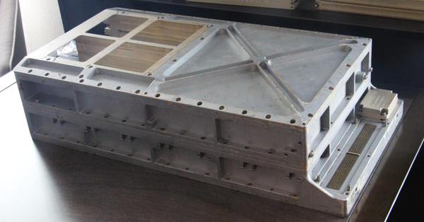
We1 are restoring the AGC shown above. It is a compact metal box with a volume of 1 cubic foot and weighs about 70 pounds. The AGC had very little memory by modern standards: 2048 words of RAM in erasable core memory and 36,864 words of ROM in core rope memory. (In this blog post, I'll discuss just the erasable core memory.) The core rope ROM modules (which we don't have)2 would be installed in the empty space on the left. On the right of the AGC, you can see the two connectors that connected the AGC to other parts of the spacecraft, including the DSKY (Display/Keyboard).3
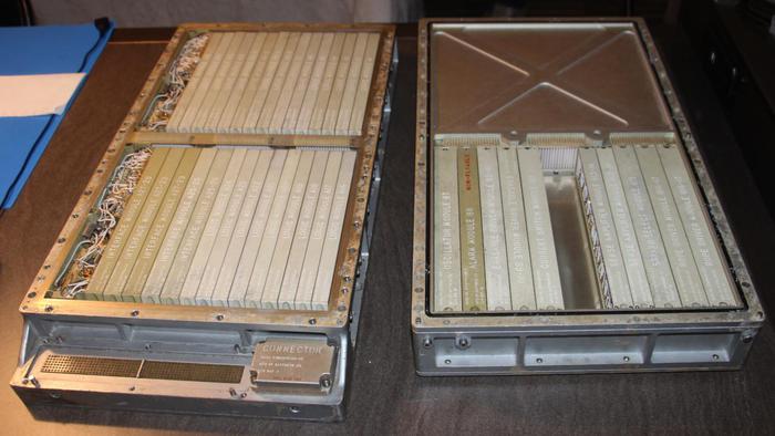
By removing the bolts holding the two trays together, we could disassemble the AGC. Pulling the two halves apart takes a surprising amount of force because of the three connectors in the middle that join the two trays. The tray on the left is the "A" tray, which holds the logic and interface modules. The tangles of wire on the left of the tray are the switching power supplies that convert 28 volts from the spacecraft to 4 and 14 volts for use in the AGC. The tray on the right is the "B" tray, which holds the memory circuitry, oscillator and alarm. The core memory module was removed in this picture; it goes in the empty slot in the middle of the B tray.
Core memory overview
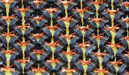
Core memory was the dominant form of computer storage from the 1950s until it was replaced by semiconductor memory chips in the early 1970s. Core memory was built from tiny ferrite rings called cores, storing one bit in each core. Cores were arranged in a grid or plane, as in the highly-magnified picture below. Each plane stored one bit of a word, so a 16-bit computer would use a stack of 16 core planes. Each core typically had 4 wires passing through it: X and Y wires in a grid to select the core, a diagonal sense line through all the cores for reading, and a horizontal inhibit line for writing.4
Each core stored a bit by being magnetized either clockwise or counterclockwise. A current in a wire through the core could magnetize the core with the magnetization direction matching the current's direction. To read the value of a core, the core was flipped to the 0 state. If the core was in 1 state previously, the changing magnetic field produced a voltage in the sense wire threaded through the cores. But if the core was in the 0 state to start, the sense line wouldn't pick up a voltage. Thus, forcing a core to 0 revealed the core's previous state (but erased it in the process).
A key property of the cores was hysteresis: a small current had no effect on a core; the current had to be above a threshold to flip the core. This was very important because it allowed a grid of X and Y lines to select one core from the grid. By energizing one X line and one Y line each with half the necessary current, only the core where both lines crossed would get enough current to flip and other cores would be unaffected. This "coincident-current" technique made core memory practical since a few X and Y drivers could control a large core plane.
The AGC's erasable core memory system
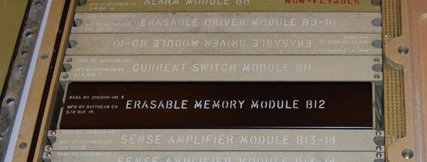
The AGC used multiple modules in the B tray to implement core memory. The Erasable Memory module (B12) contained the actual cores, 32768 cores to support 2048 words; each word was 15 bits plus a parity bit. Several more modules contained the supporting circuitry for the memory.5 The remainder of this article will describe these modules.
The photo below shows the Erasable Memory module after removing it from the tray. Unlike the other modules, this module has a black metal cover. Internally, the cores are encapsulated in Silastic (silicone rubber), which is then encapsulated in epoxy. This was intended to protect the delicate cores inside, but it took NASA a couple tries to get the encapsulation right. Early modules (including ours) were susceptible to wire breakages from vibrations. At the bottom of the modules are the gold-plated pins that plug into the backplane.
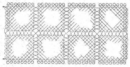
Core memory used planes of cores, one plane for each bit in the word. The AGC had 16 planes (which were called mats), each holding 2048 bits in a 64×32 grid. Note that each mat consists of eight 16×16 squares. The diagram below shows the wiring of the single sense line through a mat. The X/Y lines were wired horizontally and vertically. The inhibit line passed through all the cores in the mat; unlike the diagonal sense line it ran vertically.
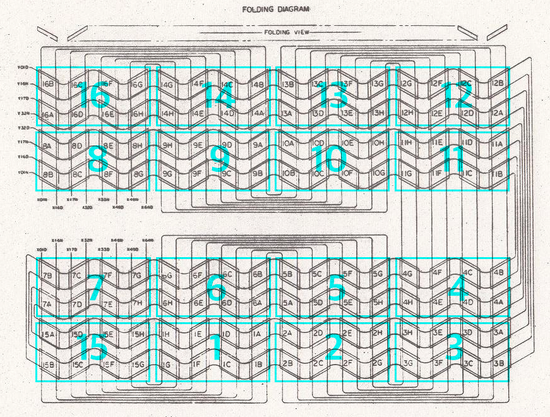
Most computers physically stacked the core planes on top of each other but the AGC used a different mechanical structure, folding the mats (planes) to fit compactly in the module. The mats were accordion-folded to fit tightly into the module as shown in the diagram below. (Each of the 16 mats is outlined in cyan.) When folded, the mats formed a block (oriented vertically in the diagram below) that was mounted horizontally in the core module.
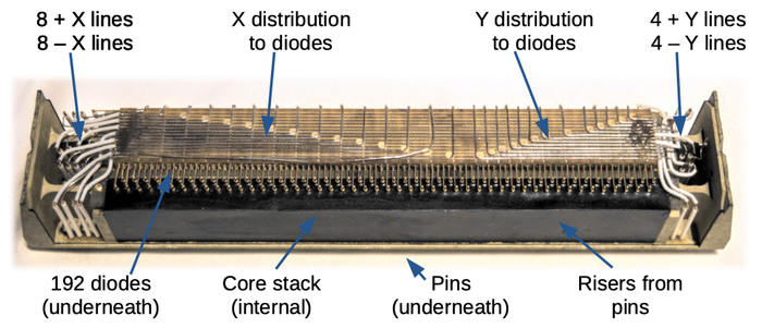
The photo below shows the memory module with the cover removed. (This is a module on display at the CHM, not our module.) Most of the module is potted with epoxy, so the cores are not visible. The most noticeable feature is the L-shaped wires on top. These connect the X and Y pins to 192 diodes. (The purpose of the diode will be explained later.) The diodes are hidden underneath this wiring in two layers, mounted horizontally cordwood-style. The leads from the diodes are visible as they emerge and connect to terminals on top of the black epoxy.
Marc took X-rays of the module and I stitched the photos together (below) to form an image looking down into the module. The four rows of core mats in the folding diagram correspond to the four dark blocks. You can also see the two rows of diodes as two darker horizontal stripes. At this resolution, the wires through the cores and the tangled mess of wires to the pins are not visible; these wires are very thin 38-gauge wires, much thinner than the wires to the diodes.
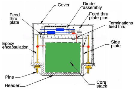
The diagram below shows a cross-section of the memory module. (The front of the module above corresponds to the right side of the diagram.) The diagram shows how the two layers of diodes (blue) are arranged at the top, and are wired (red) to the core stack (green) through the "feed thru". Also note how the pins (yellow) at the bottom of the module rise up through the epoxy and are connected by wires (red) to the core stack.
Addressing a memory location
The AGC's core memory holds 2048 words in a 64×32 matrix. To select a word, one of the 64 X select lines is energized along with one of the 32 Y select lines. One of the challenges of a core memory system is driving the X and Y select lines. These lines need to be driven at high current (100's of milliamps). In addition, the read and write currents are opposite directions, so the lines need bidirectional drivers. Finally, the number of X and Y lines is fairly large (64 + 32 for the AGC), so using a complex driver circuit on each line would be too bulky and expensive. In this section, I'll describe the circuitry in the AGC that energizes the right select lines for a particular address.
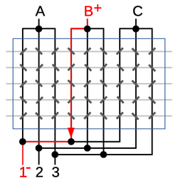
The AGC uses a clever trick to minimize the hardware required to drive the X and Y select lines. Instead of using 64 X line drivers, the AGC has 8 X drivers at the top of the matrix, and 8 at the bottom of the matrix. Each of the 64 select lines is connected to a different top and bottom driver pair. Thus, energizing a top driver and a bottom driver produces current through a single X select line. Thus, only 8+8 X drivers are required rather than 64.6 The Y drivers are similar, using 4 on one side and 8 on the other. The downside of this approach is 192 diodes are required to prevent "sneak paths" through multiple select lines.7
The diagram above demonstrates this technique for the vertical lines in a hypothetical 9×5 core array. There are three "top" drivers (A, B and C), and three "bottom" drivers (1, 2 and 3). If driver B is energized positive and driver 1 is energized negative, current flows through the core line highlighted in red. Reversing the polarity of the drivers reverses the current flow, and energizing different drivers selects a different line. To see the need for diodes, note that in the diagram above, current could flow from B to 2, up to A and finally down to 1, for instance, incorrectly energizing multiple lines.
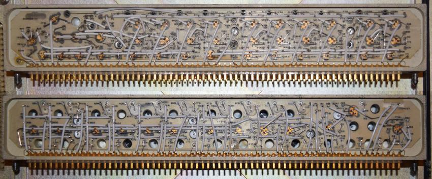
The address decoder logic is in tray "A" of the AGC, implemented in several logic modules.9 The AGC's logic is entirely built from 3-input NOR gates (two per integrated circuit), and the address decoder is no exception. The image below shows logic module A14. (The other logic modules look essentially the same, but the internal printed circuit board is wired differently.) The logic modules all have a similar design: two rows of 30 ICs on each side, for 120 ICs in total, or 240 3-input NOR gates. (Module A14 has one blank location on each side, for 118 ICs in total.) The logic module plugs into the AGC via the four rows of pins at the bottom.10
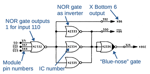
The diagram below shows the circuit to generate one of the select signals (XB6—X bottom 6).11 The NOR gate outputs a 1 if the inputs are 110 (i.e. 6). The other select signals are generated with similar circuits, using different address bits as inputs.
Each integrated circuit implemented two NOR gates using RTL (resistor-transistor logic), an early logic family. These ICs were costly; they cost $20-$30 each (around $150 in current dollars). There wasn't much inside each IC, just three transistors and eight resistors. Even so, the ICs provided a density improvement over the planned core-transistor logic, making the AGC possible. The decision to use ICs in the AGC was made in 1962, amazingly just four years after the IC was invented. The AGC was the largest consumer of ICs from 1962 to 1965 and ended up being a major driver of the integrated circuit industry.
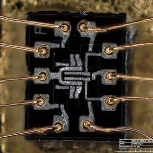
The die photo below shows the internal structure of the NOR gate; the metal layer of the silicon chip is most visible.12 The top half is one NOR gate and the bottom half is the other. The metal wires connect the die to the 10-pin package. The transistors are clumped together in the middle of the chip, surrounded by the resistors.
Erasable Driver Modules
Next, the Erasable Driver module converts the 4-volt logic-level signals from the address decoder into 14-volt pulses with controlled current. The AGC has two identical Erasable Driver modules, in slots B9 and B10.5 Two modules are required due to the large number of signals: 28 select lines (X and Y, top and bottom), 16 inhibit lines (one for each bit), and a dozen control signals.
The select line driver circuits are simple transistor switching circuits: a transistor and two resistors. Other circuits, such as the inhibit line drivers are a bit more complex because the shape and current of the pulse need to be carefully matched to the core module. This circuit uses three transistors, an inductor, and a handful of resistors and diodes. The resistor values are carefully selected during manufacturing to provide the desired current.
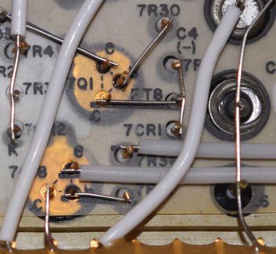
This module, like the other non-logic modules, is built using cordwood construction. In this high-density construction, components were inserted into holes in the module, passing through from one side of the module to the other, with their leads exiting on either side. (Except for transistors, with all three leads on the same side.) On each side of the module, point-to-point wiring connected the components with welded connections. In the photo below, note the transistors (golden, labeled with Q), resistors (R), diodes (CR for crystal rectifier, with K indicating the cathode), large capacitors (C), inductor (L), and feed-throughs (FT). A plastic sheet over the components conveniently labels them; for instance, "7Q1" means transistor Q1 for circuit 7 (of a repeated circuit). These labels match the designations on the schematic. At the bottom are connections to the module pins. Modules that were flown on spacecraft were potted with epoxy so the components were protected against vibration. Fortunately, our AGC was used on the ground and left mostly unpotted, so the components are visible.
Current Switch Module
You might expect that the 14-volt pulses from the Erasable Driver modules would drive the X and Y lines in the core. However, the signals go through one more module, the Current Switch module, in slot B11 just above the core memory module. This module generates the bidirectional pulses necessary for the X and Y lines.
The driver circuits are very interesting as each driver includes a switching core in the circuit. (These cores are much larger than the cores in the memory itself.)13 The driver uses two transistors: one for the read current, and the other for the write current in the opposite direction. The switching core acts kind of like an isolation transformer, providing the drive signal to the transistors. But the switching core also "remembers" which line is being used. During the read phase, the address decoder flips one of the cores. This generates a pulse that drives the transistor. During the write phase, the address decoder is not involved. Instead, a "reset" signal is sent through all the driver cores. Only the core that was flipped in the previous phase will flip back, generating a pulse that drives the other transistor. Thus, the driver core provides memory of which line is active, avoiding the need for a flip flop or other latch.
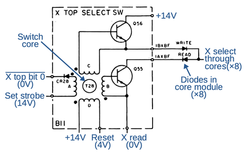
The diagram below shows the schematic of one of the current switches. The heart of the circuit is the switching core. If the driver input is 1, winding A will flip the the core when the set strobe is pulsed. This will produce a pulses on the other windings; the positive pulse on winding B will turn on transistor Q55, pulling the output X line low for reading.14 The output is connected via eight diodes to eight X top lines through the core. A similar bottom select switch (without diodes) will pull X bottom lines high; the single X line with the top low and the bottom high will be energized, selecting that row. For a write, the reset line is pulled low energizing winding D. If the core had flipped earlier, it will flip back, generating a pulse on winding C that will turn on transistor Q56, and pull the output high. But if the core had not flipped earlier, nothing happens and the output remains inactive. As before, one X line and one Y line through the core planes will be selected, but this time the current is in the opposite direction for a write.
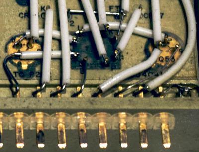
The photo below shows one of the current switch circuits and its cordwood construction. The switching core is the 8-pin black module between the transistors. The core and the wires wound through it are encapsulated with epoxy, so there's not much to see. At the bottom of the photo, you can see the Malco Mini-Wasp pins that connect the module to the backplane.
Sense Amplifier Modules
When a core flips, the changing magnetic field induces a weak signal in the corresponding sense line. There are 16 sense lines, one for each bit in the word. The 16 sense amplifiers receive these signals, amplify them, and convert them to logic levels. The sense amplifiers are implemented using a special sense amplifier IC. (The AGC used only two different ICs, the sense amplifier and the NOR gate.) The AGC has two identical sense amplifier modules, in slots B13 and B14; module B13 is used by the erasable core memory, while B14 is used by the fixed memory (i.e. core rope used for ROM).
The signal from the core first goes through an isolation transformer. It is then amplified by the IC and the output is gated by a strobe transistor. The sense amplifier depends on carefully-controlled voltage levels for bias and thresholds. These voltages are produced by voltage regulators on the sense amplifier modules that use Zener diodes for regulation. The voltage levels are tuned during manufacturing by selecting resistor values and optional diodes, matching each sense amplifier module to the characteristics of the computer's core memory module.
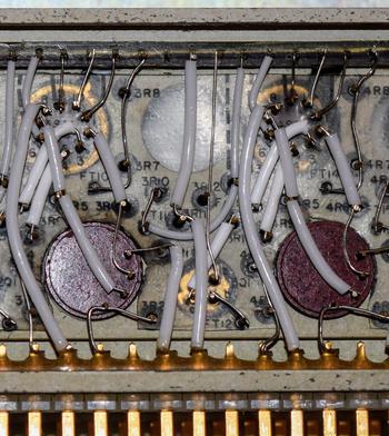
The photo below shows one of the sense amp modules. The eight repeated units are eight sense amplifiers; the eight other sense amplifiers are on the other side of the module. The reddish circles are the pulse transformers, while the lower circles are the sense amplifier ICs. The voltage regulation is in the middle and right of the module. On top of the module (front in the photo) you can see the horizontal lines of the nickel ribbon that connects the circuits; it is somewhat similar to a printed circuit board.
The photo below shows a closeup of the module. At the top are two amplifier integrated circuits in metal cans. Below are two reddish pulse transformers. An output driver transistor is between the pulse transformers.15 The resistors and capacitors are mounted using cordwood construction, so one end of the component is wired on this side of the module, and one on the other side. Note the row of connections at the top of the module; these connect to the nickel ribbon interconnect.
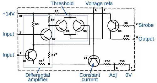
The diagram below shows the circuitry inside each sense amp integrated circuit. The sense amp chip is considerably more complex than the NOR gate IC. The chip receives the sense amp signal inputs from the pulse transformer and the differential amplifier amplifies the signal.16 If the signal exceeds a threshold, the IC outputs a 1 bit when clocked by the strobe.
Writes
With core memory, the read operation and write operation are always done in pairs. Since a word is erased when it is read, it must then be written, either with the original value or a new value. In the write cycle, the X and Y select lines are energized to flip the core to 1, using the opposite current from the read cycle.
Since the same X and Y select lines go through all the planes, all bits in the word would be set to 1. To store a 0 bit, each plane has an inhibit line that goes through all the cores in the plane. Energizing the inhibit line in the opposite direction to the X and Y select lines partially cancels out the current and prevents the core from receiving enough current to flip it, so the bit remains 0. Thus, by energizing the appropriate inhibit lines, any value can be written to the word in core. The 16 inhibit lines are driven by the Erasable Driver modules.
The broken wire
During the restoration, we tested the continuity of all the lines through the core module. Unfortunately, we discovered that the inhibit line for bit 16 is broken internally. NASA discovered in early testing that wires could be sheared inside the module, due to vibrations between the silicone encapsulation and the epoxy encapsulation. They fixed this problem in the later modules that were flown, but our module had the original faulty design. We attempted to find the location of the broken wire with X-rays, but couldn't spot the break. Time-domain reflectometry suggests the break is inconveniently located in the middle of the core planes. We are currently investigating options to deal with this. Marc has a series of AGC videos; the video below provides detail on the broken wire in the memory module.
Conclusion
Core memory was the best storage technology in the 1960s and the Apollo Guidance Computer used it to get to the Moon. In addition to the core memory module itself, the AGC required several modules of supporting circuitry. The AGC's logic circuits used early NOR-gate integrated circuits, while the analog circuits were built from discrete components and sense amplifier ICs using cordwood construction.
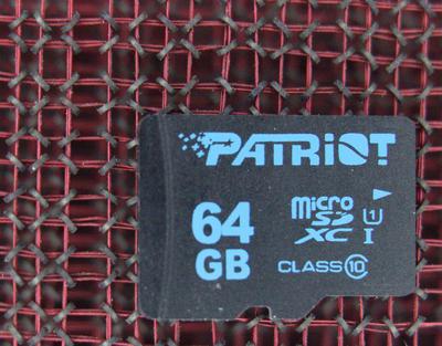
The erasable core memory in the AGC stored just 2K words. Because each bit in core memory required a separate physical ferrite core, density was limited. Once semiconductor memory became practical in the 1970s, it rapidly replaced core memory. The image below shows the amazing density difference between semiconductor memory and core memory: 64 bits of core take about the same space as 64 gigabytes of flash.
I announce my latest blog posts on Twitter, so follow me @kenshirriff for future articles. I also have an RSS feed. See the footnotes for Apollo manuals17 and more information sources18. Thanks to Mike Stewart for supplying images and extensive information.
Notes and references
-
The AGC restoration team consists of Mike Stewart (creator of FPGA AGC), Carl Claunch, Marc Verdiell (CuriousMarc) on YouTube and myself. The AGC that we're restoring belongs to a private owner who picked it up at a scrap yard in the 1970s after NASA scrapped it. For simplicity I refer to the AGC we're restoring as "our AGC".
The Apollo flights had one AGC in the command module (the capsule that returned to Earth) and one AGC in the lunar module. In 1968, before the Moon missions, NASA tested a lunar module (with astronauts aboard) in a giant vacuum chamber in Houston to ensure that everything worked in space-like conditions. We believe our AGC was installed in that lunar module (LTA-8). Since this AGC was never flown, most of the modules are not potted with epoxy. ↩
-
We don't have core rope modules, but we have a core rope simulator from the 1970s. Yes, we know about Francois; those are ropes for the earlier Block I Apollo Guidance Computer and are not compatible with our Block II AGC. ↩
-
Many people have asked if we talked to Fran about the DSKY. Yes, we have. ↩
-
There were alternative ways to wire a core plane. Using a diagonal sense wire reduced the noise in the sense wire from X and Y pulses but some used a horizontal sense wire. Some core systems used the same wire for sense and inhibit (which simplified manufacturing), but that made noise rejection more complex. ↩
-
If you look carefully at the pictures of modules installed in the AGC, the Erasable Driver module in B10 is upside down. This is not a mistake, but how the system was designed. I assume this simplified the backplane wiring somehow, but it looks very strange. ↩
-
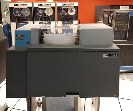
The IBM 1401 business computer, for example, used a different approach to generate the X and Y select lines. To generate the 50 X select signals, it used a 5×10 matrix of cores (separate from the actual memory cores). Two signals into the matrix were energized at the same time, flipping one of the 50 cores and generating a pulse on that line. Thus, only 5+10 drivers were needed instead of 50. The Y select signals were similar, using an 8×10 matrix. Details here. ↩
-
The AGC core memory required 192 diodes to prevent sneak paths, where a pulse could go backward through the wrong select lines. Each line required two diodes since the lines are driven one direction for read and the opposite for write. Since there are 64 X lines and 32 Y lines, 2×(64+32) = 192 diodes were required. These diodes were installed in two layers in the top of the core memory module. ↩
-
The memory address is mapped onto the select lines as follows. The eight X bottom signals are generated from the lowest address bits, S01, S02 and S03. (Bits in a word are numbered starting at 1, not 0.) Each decoder output has as NOR gate to select a particular bit pattern, along with four more NOR gates as buffers. The eight X top signals are generated from address bits S04, S05, and S06. The four Y bottom signals are generated from address bits S07 and S08. The eight Y top signals are generated from address bits EAD09, EAD10, and EAD11; these in turn were generated from S09 and S10 along with bank select bits EB9, EB10 and EB11. (The AGC used 12-bit addresses, allowing 4096 words to be addressed directly. Since the AGC had 38K of memory in total, it had a complex memory bank system to access the larger memory space.) ↩
-
For address decoding, the X drivers were in module A14, the Y top drivers were in A7 and the Y bottom drivers in A14. The memory address was held in the memory address register (S register) in module A12, which also held a bit of decoding logic. Module A14 also held some memory timing logic. In general, the AGC's logic circuits weren't cleanly partitioned across modules since making everything fit was more important than a nice design. ↩
-
One unusual thing to notice about the AGC's logic circuitry is there are no bypass capacitors. Most integrated circuit logic has a bypass capacitor next to each IC to reduce noise, but NASA found that the AGC worked better without bypass capacitors. ↩
-
The "Blue-nose" gate doesn't have the pull-up resistor connected, making it open collector. It is presumably named after its blue appearance on blueprints. Blue-nose outputs can be connected together to form a NOR gate with more inputs. In the case of the address decoder, the internal pull-up resistor is not used so the Erasable Driver module (B9/B10) can pull the signal up to BPLUS (+14V) rather than the +4V logic level. ↩
-
The AGC project used integrated circuits from multiple suppliers, so die photos from different sources show different layouts. ↩
-
The memory cores and the switching core were physically very different. The cores in the memory module had a radius between 0.047 and 0.051 inches (about 1.2mm). The switching cores were much larger (either .249" or .187" depending on the part number) and had 20 to 50 turns of wire through them. ↩
-
For some reason, the inputs to the current switches are numbered starting at 0 (XT0E-XT7E) while the outputs are numbered starting at 1 (1AXBF-8AXBF). Just in case you try to understand the schematics. ↩
-
The output from the sense amplifiers is a bit confusing because the erasable core memory (RAM) and fixed rope core memory (ROM) outputs are wired together. The RAM has one sense amp module with 16 amplifiers in slot B13, and the ROM has its own identical sense amp module in slot B14. However, each module only has 8 output transistors. The two modules are wired together so 8 output bits are driven by transistors in the RAM's sense amp module and 8 output bits are driven by transistors in the ROM's sense amp module. (The motivation behind this is to use identical sense amp modules for RAM and ROM, but only needing 16 output transistors in total. Thus, the transistors are split up 8 to a module.) ↩
-
I'll give a bit more detail on the sense amps here. The key challenge with the sense amps is that the signal from a flipping core is small and there are multiple sources of noise that the sense line can pick up. By using a differential signal (i.e. looking at the difference between the two inputs), noise that is picked up by both ends of the sense line (common-mode noise) can be rejected. The differential transformer improved the common-mode noise rejection by a factor of 30. (See page 9-16 of the Design Review.) The other factor is that the sense line goes through some cores in the same direction as the select lines, and through some cores the opposite direction. This helps cancel out noise from the select lines. However, the consequence is that the pulse on the sense line may be positive or may be negative. Thus, the sense amp needed to handle pulses of either polarity; the threshold stage converted the bipolar signal to a binary output. ↩
-
The Apollo manuals provide detailed information on the memory system. The manual has a block diagram of the AGC's memory system. The address decoder is discussed in the manual starting at 4-416 and schematics are here. Schematics of the Erasable Driver modules are here and here; the circuit is discussed in section 4-5.8.3.3 of the manual. Schematics of the Current Switch module are here and here; the circuit is discussed in section 4-5.8.3.3 of the manual. Sense amplifiers are discussed in section 4-5.8.3.4 of the manual with schematics here and here; schematics are here and here. ↩
-
For more information on the AGC, the Virtual AGC site has tons of information on the AGC, in particular the ElectroMechanical page has lots of schematics and drawings. There's a video of Eldon Hall, designer of the AGC, disassembling our AGC in 2004. If you want to try a simulated AGC in your browser, see moonjs.
Eldon Hall's book Journey to the Moon: The History of the Apollo Guidance Computer is very interesting. Also see Sunburst and Luminary: An Apollo Memoir by Don Eyles, who wrote a lot of the lunar landing code and discusses the famous program alarms. The Apollo Guidance Computer: Architecture and Operation is unevenly written and has errors, but the discussion in the last half of space navigation and a lunar mission is informative. ↩
