Accounting machines, the IBM 1403, and why printers standardized on 132 columns

Have you ever wondered why 132 characters is such a common width for printers? Many printers produced lines of 132 characters, such as the groundbreaking Centronics 101 dot-matrix printer (1970), the ubiquitous DECwriter II terminal (1975), the Epson MX-80 dot-matrix printer (1981), and the Apple Daisy Wheel Printer (1983). Even CRT terminals such as the DEC VT100 (1978) supported 132 columns. But why the popularity of 132 columns?1

After researching this question, I've concluded that there are two answers. The first answer is that there isn't anything special about 132 columns. In particular, early printers used an astoundingly large variety of line widths including 50, 55, 60, 70, 73, 80, 88, 89, 92, 100, 118, 120, 128, 130, 136, 140, 144, 150 and 160 characters.2 This shows there was no strong technical or business reason to use 132 columns. Instead, 132 columns became a de facto standard due to the popularity of the IBM 1401 computer and its high-performance 1403 line printer, which happened to print 132 columns.

The second, more interesting, answer is that a variety of factors in the history of data processing, some dating back a century, led to standardization on several sizes for printed forms. One of these sizes became standard line printer paper holding 132 columns.

The IBM 1401 computer and the 1403 printer

The first printer to use 132 columns appears to be the IBM 1403 line printer, which provided output for the IBM 1401 business computer. The IBM 1401 was the most popular computer of the early 1960s, largely due to its low price. Earlier computers had been limited to large corporations due to their high cost; the IBM 705 business computer rented for $43,000 a month (almost $400,000 in current dollars). But the IBM 1401 could be rented for $2500 per month, opening up the market to medium-sized businesses that used it for payroll, inventory, accounting and many other business tasks. As a result, over 10,000 IBM 1401 computers were in use by the mid-1960s.

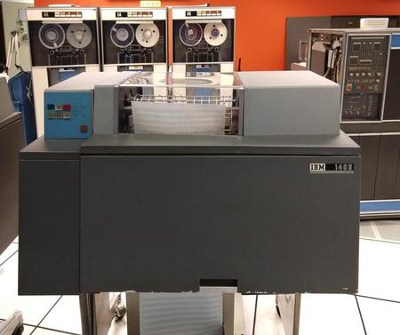
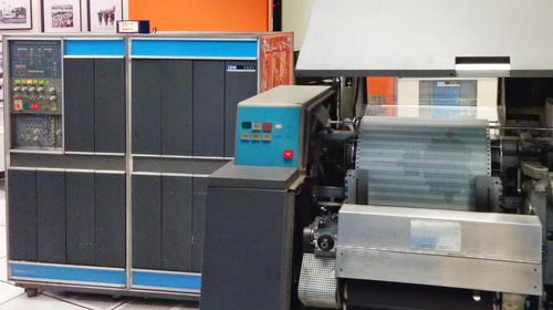
The IBM 1403 printer in front of the popular 1401 business computer (right) and 729 tape drives (left).

The IBM 1403 printer in front of the popular 1401 business computer (right) and 729 tape drives (left).

The IBM 1403 printer was an important part of the 1401's success. This high-speed line printer could print 600 lines per minute of high-quality text, said to be the best print quality until laser printers.10 "Even today, [the 1403 printer] remains the standard of quality for high-speed impact printing," at least according to IBM. By the late 1960s, half of the world's continuous forms were printed on IBM 1403 printers.3

Because the IBM 1403 printer was so popular, its 132-column format became a de facto standard, supported by later printers and terminals for backward compatibility. The 14 7/8"×11" green-bar paper that it used4 remains popular to this day, available at office supply stores.5

Accounting machines / tabulators

Now I'll discuss the history that led up to 132 columns on 14 7/8" paper. The key actor in this story is the electric accounting machine or tabulator. While these machines are mostly forgotten now, they were the cornerstone of business data processing in the pre-computer era (history). Tabulators date back to the 1890 census when Herman Hollerith invented these machines to tabulate (i.e. count)6 data stored on punch cards. Later tabulators used relays and electromechanical counters to sum up values, were "programmed" for different tasks by a plugboard of wires, and could process 150 punch cards per minute.

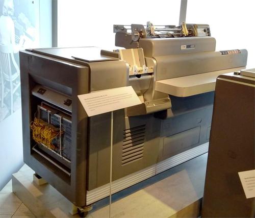
The IBM 403 electric accounting machine. Note the programming plugboard at left with yellow wires. The printer carriage is on top. Cards are fed into the hopper to the left.

The IBM 403 electric accounting machine. Note the programming plugboard at left with yellow wires. The printer carriage is on top. Cards are fed into the hopper to the left.

By 1943, tabulators were popular with businesses and governments; IBM had about 10,000 tabulators in service. These machines were complex, able to handle conditionals while adding or subtracting three levels of subtotals and formatting their alphanumeric output. Accounting machines were used for a wide variety of business data processing tasks such as accounting, inventory, billing, issuing checks, printing shipping labels or even printing W-2 tax forms. While these machines were designed for businesses, tabulators were also pressed into service for scientific computation in the 1930s and 1940s, most famously for nuclear bomb simulations during the Manhattan Project.

IBM 285 accounting machine (1933)

The earliest tabulators displayed the results on mechanical counters so an operator had to write down the results after each subtotal (details). The development of the tabulator printing unit in the 1920s eliminated this inconvenient manual step. One popular printing tabulator was the IBM 285, introduced in 1933. This machine printed values using 3 to 7 "print banks", where each bank consisted of 10 numeric type bars.7 The output below shows 7 column-output, generated by a 285 tabulator with 7 print banks.

Output from the IBM 285 Electric Accounting Machine, showing its 7 columns of counter output. This output is standard typewriter spacing (6 lines per inch), double-spaced. Headings are pre-printed on the form, not printed by the tabulator.

Output from the IBM 285 Electric Accounting Machine, showing its 7 columns of counter output. This output is standard typewriter spacing (6 lines per inch), double-spaced. Headings are pre-printed on the form, not printed by the tabulator.

The character spacing was 5/32" (a value that will be important later), yielding columns 1 7/8" wide. This spacing was about 50% wider than standard typewriter spacing (10 characters per inch) even though the tabulator used standard typewriter line spacing (6 lines per inch). As you can see from the output above, this caused large gaps between the characters. So why did the accounting machine use a character spacing of 5/32"? To understand that, we have to go back a decade.

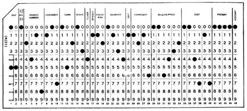
Early IBM punch cards had 45 columns with round holes spaced 5/32" apart.8 The image below shows one of these cards. Each column contained one hole, representing a digit from 0 to 9. One machine used with punch cards was the "interpreter". It read a card and printed the card's contents at the top of the card above the holes. The interpreter used a 45-column print mechanism with type bars spaced 5/32" apart to match the holes.

An IBM 45-column punch card from the early 1920s. This card used round holes, unlike the rectangular holes on "modern" 80-column punch cards. From Electric Tabulating Machines.

An IBM 45-column punch card from the early 1920s. This card used round holes, unlike the rectangular holes on "modern" 80-column punch cards. From Electric Tabulating Machines.

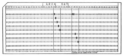
In 1928, IBM introduced the "modern" punch card, which held 80 columns of data (below). These cards used rectangular holes so the holes could be closer together (0.087" spacing). However, IBM kept many of the mechanisms designed for 45-column cards, along with their 5/32" spacing. The result was mismatched products like the IBM 550 Interpreter (1930) that read an 80-column punch card and printed 45 characters at the top of the card. As a result, the characters didn't line up with the holes, as you can see below.9 Likewise, The 285 accounting machine used a type bar printer with 5/32" spacing, even though it used 80-column cards.

The IBM 550 card interpreter read data punched into an 80-column card and printed 45 columns of that data at the top of the card.

The IBM 550 card interpreter read data punched into an 80-column card and printed 45 columns of that data at the top of the card.

IBM 405 (1934) and 402 (1948) accounting machines

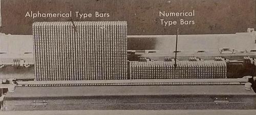
The IBM 285 tabulator could only print digits, but in 1934, IBM introduced the 405, a tabulator that could print alphanumeric information, followed by the improved 402 accounting machine in 1948. Alphanumeric output greatly expanded the uses of the tabulator, as it could print invoices, address labels, employee records, or other forms that required alphanumeric data. The IBM 405 had 88 type bars that moved vertically to print a line of output (below).18 Note the gap for a ribbon guide between the two blocks of type bars.

The IBM 405 accounting machine printed with type bars: 43 alphanumeric ("alphamerical") type bars on the left, and 45 numeric-only type bars on the right. From Electric punched card accounting machines.

The IBM 405 accounting machine printed with type bars: 43 alphanumeric ("alphamerical") type bars on the left, and 45 numeric-only type bars on the right. From Electric punched card accounting machines.

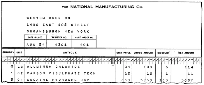
The figure below shows sample output from a 405 tabulator, showing alphanumeric characters on the left side. As with the earlier tabulators, the 5/32" character width resulted in widely separated characters. Note that the headers and boxes were not printed by the tabulator, but were pre-printed on the form.

Output from the IBM 405 tabulator, showing a billing statement. Apparently cocaine was a common product back then. (Electronic Accounting Machines page 17-19.)

Output from the IBM 405 tabulator, showing a billing statement. Apparently cocaine was a common product back then. (Electronic Accounting Machines page 17-19.)

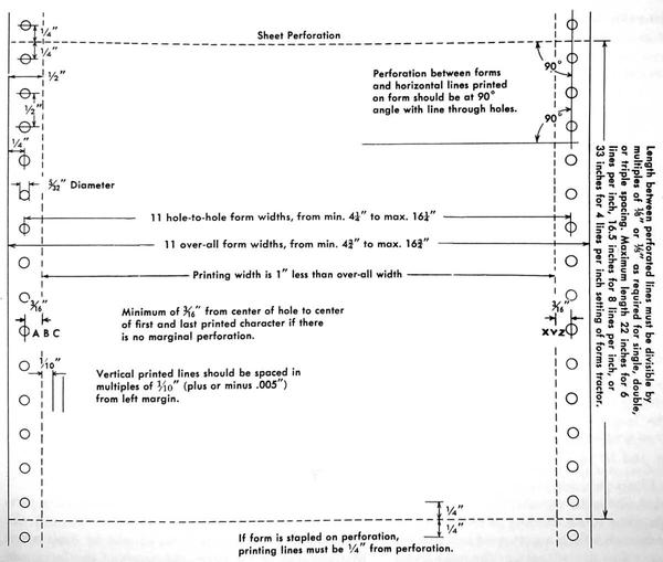
At first forms were hand-fed sheets of paper, but for convenience these were soon replaced by continuous-feed forms.12 To keep forms from slipping out of alignment, holes were added along the sides so forms could be fed by pin-feed or tractor-feed mechanisms. These forms often used a removable 1/2" perforated strip on each side containing the feed holes.22 Thus, the hole-to-hole width was 1/2" less than the overall width, and the printable region was 1" less than the overall width.

Businesses would order customized forms for their particular needs, but these forms were usually produced in standardized widths, given below.11 Surprisingly, these arbitrary-seeming form sizes are still standard sizes available today. Many of the standard form widths are round numbers such as 8" and 11", but there are also strange numbers such as 12 27/32" and 18 15/16".13 I explain most of these sizes in the footnotes.1516 Note that most of the unusual widths are multiples of the 5/32" character width (hole-to-hole); I've highlighted these in yellow. I believe making the width a multiple of 5/32" was a deliberate choice.14

Standard form widths, from the 402 manual, page 151.

Standard form widths, from the 402 manual, page 151.

The 402's 88 character output fit exactly onto a 14 7/8" wide form, while also being a multiple of 5/32" (hole-to-hole).17 I believe that this was the reason that 14 7/8" paper became a standard. This width is the dimension of standard green-bar line printer paper still used today, so this dimension is very important. Note that this paper size became a standard before commercial computers even existed.

IBM 407 accounting machine (1949)

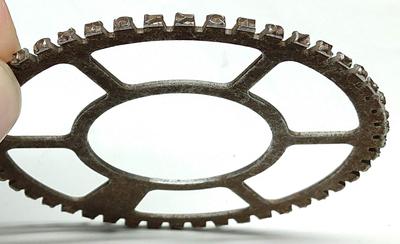
The successor to the IBM 402 accounting machine was the IBM 407 accounting machine, introduced in 1949. The most important feature from our perspective was the move from type bars to type wheels. Each type wheel had 47 characters (letters, numbers and symbols) around the circumference and rotated at high speed to print the correct character.19 The tabulator used 120 of these wheels to print a line of 120 characters.

Type wheel from an IBM 407 accounting machine.

Type wheel from an IBM 407 accounting machine.

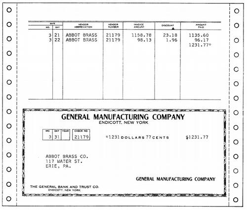
The narrow type wheels enabled the 407 to print 10 characters per inch (standard typewriter pica pitch). The output below shows how the tabulator could issue checks using pre-printed forms. Note that the 407's output looks like normal typing compared to the widely spaced characters of the earlier 405 and 402.

Sample output from an IBM 407 accounting machine. Character spacing is much more natural than the earlier 402 output. Sprocket-fed forms are now common. Figure 128 from Manual of Operation.

Sample output from an IBM 407 accounting machine. Character spacing is much more natural than the earlier 402 output. Sprocket-fed forms are now common. Figure 128 from Manual of Operation.

The 407 operating manual described how to design forms for the 407,20 and listed eleven standard form sizes (below).21 Despite the switch from 5/32" characters to much narrower 0.1" characters, most of the new standard form widths matched the earlier 402 widths (indicated in green). Many of the previous strange form widths (such as 17 25/32") were dropped, but 13 5/8" and 14 7/8" were preserved, which will prove important.

Standard widths for forms for the IBM 407. From 407 Operating Manual page 187.

Standard widths for forms for the IBM 407. From 407 Operating Manual page 187.

The IBM 1403 printer (1959) and its 132 columns

Finally we arrive at the 1403 line printer (1959). This printer supported line widths of 100 character, 120 characters, and 132 characters at 10 characters per inch. The 120 character line is obviously useful for backward compatibility with the 407. But what about 132 characters?

Note that the 13 5/8" form conveniently fit the 407's (or 1403's) 120 character line with a small margin.23 The next-larger standard form width was 14 7/8". The increase of 1.25 inches allows you to add 12.5 characters.24 Thus, the jump from 120 to 132 characters was an obvious product improvement since it makes use of the next standardized form width. One objection is that 130 seems like a more sensible round number—the UNIVAC printer used 130 characters per line—so why not use 130 instead of 132? Due to the complex alignment between the 1403's chain and the print hammers, a line width divisible by 3 (such as 132) works out better.25 I suspect this is the primary reason that the IBM 1403 used 132 characters rather than 130.26 A width of 128 might seem better because of binary, but it's not; the 1401 was a decimal machine so there's no benefit to 128.27

The IBM 1403 printer generating a Mandelbrot set on standard 14 7/8"×11" green-bar paper. The IBM 1401 computer is at the left.

The IBM 1403 printer generating a Mandelbrot set on standard 14 7/8"×11" green-bar paper. The IBM 1401 computer is at the left.

Conclusion

To summarize my hypothesis,28 the 132-character line on 14 7/8" wide paper has its roots in the dimensions of punch cards over a century ago. IBM's early 45-column punch cards resulted in the creation of a printing mechanism with a wide character spacing of 5/32" to match the punch card hole spacing. Even though IBM moved to 80-column cards in 1928, accounting machines continued to use 5/32" characters in the 1930s and 1940s. This resulted in standardized form widths, most importantly 14 7/8" which fit a line of 88 characters. In 1949, IBM's tabulators moved to a standard 10 characters per inch spacing. With that character size and 14 7/8" paper, a 132-character line is natural, and this was implemented on the IBM 1403 printer in 1959.

Because the 1403 printer was wildly popular, 132 character lines on 14 7/8" paper became a de facto standard supported by many other companies. This is why even though punch cards are long obsolete, you can easily buy 14 7/8" green-bar line printer paper to this day.

I announce my latest blog posts on Twitter, so follow me at @kenshirriff for future articles. I also have an RSS feed. I've written about accounting machines before, here and here, if you want to learn more. Thanks to Dag Spicer and Sydney Olson (CHM) and Max Campbell (IBM Archives) for research assistance.

Notes and references

  1. I've been wondering about 132 columns for a long time. I asked the 1401 restoration team about 132 columns a while ago, but didn't get any solid answers. Retrocomputing StackExchange discussed the source of 132 columns last year, but I find the answers unconvincing. 

  2. It's interesting to look at the history of printers and their assorted line widths.

    IBM kept old printing technology around for decades. The print mechanism from the 407 (1949) was reused in the IBM 716 and 717 printers for the IBM 700 series vacuum tube mainframes (1952+) and the IBM 7000 series transistorized mainframes (1958+). The IBM 407 was also used as an output unit for the IBM 650 drum-based computer (1955) and IBM 305 RAMAC disk-based computer (1956). The IBM 1132 printer for the low-end IBM 1130 computer (1965) also used the 407's print mechanism.

    IBM introduced high-speed wire printers (i.e. dot matrix) in 1955, which output 1000 lines per minute; the 719 printer had 60 column output, while the 730 had 120 columns. Unlike modern dot matrix printers, these printers had multiple print heads (30 or 60) for high speed. Unfortunately, these printers were unreliable and a commercial failure. (For details see pages 484-486 of IBM's Early Computers and the Manual of Operation.)

    The RAMAC system (1956) used the IBM 370 printer (unrelated to the later IBM System/370 mainframe), which printed 80 character lines at 10 characters per inch. This printer was very slow; it took about 2 seconds to print a line using a single octagonal typestick (manual).

    In 1970, IBM introduced the IBM System/370 along with the IBM 3211, a new high-speed (2000 lines per minute) line printer. This printer had 132 columns or optionally 150. It was similar to a chain printer except it used a train of character slugs.

    I don't have as much information on non-IBM printers, but in 1954, Remington Rand introduced the first high-speed drum printer, the "High Speed Off Line Printer System" for the UNIVAC computer. This printer produced 600 lines per minute at 130 characters per line. The printer used 18 kW of power and was cooled by 8 gallons per minute of chilled water (details, details). As far as other manufacturers, Analex produced a 120-column line printer. Bull had a printer with 80 print bars and a 92-character alphabetical printer Samsatronic had a 140-character dot matrix printer in the 1950s. Burroughs introduced a fast (1000 line per minute) dot matrix printer (called a wire printer) in 1954 that printed 100 character lines. The Burroughs 220 High-Speed Printer System (1959) used a drum to produce 120 character lines at 1225 lines per minute.

    For an extensive history of printers, see Print Unchained: 50 Years of Digital Printing, 1950-2000 and Beyond. IBM's Early Computers has a detailed discussion of the history and development of IBM printers (Chapter 12.4). It doesn't mention the reason behind different line lengths, unfortunately. For information on printing dimensions of IBM's printers of the 1970s, see Form Design Reference Guide for Printers. More information on early printers can also be found in The U.S. Computer Printer Industry

  3. The estimate that half of the continuous forms volume was printed on IBM 1403 printers is from Print Unchained: 50 Years of Digital Printing, 1950-2000 and Beyond page 102. The estimate is attributed to "one observer" at "some point in the latter 1960s." The IBM 1403 had a long life; IBM 360 and IBM 370 mainframe systems used it into the 1970s. 

  4. As a measure of the popularity of 14 7/8" forms, in 1971 that width was estimated to make up 50% of forms. (Computer Industry Annual, 1971, p309.) 

  5. Although line printers are best known for using 14 7/8" wide paper, the IBM 1403 printer supported forms from 3 1/2" to 18 3/4" wide; see IBM 1403 Printer Component Description pages 11 and 12. Note that the printable region is 13.2", so forms can be much wider than the printable region. 

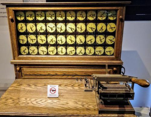
  6. Confusingly the word "tabulator" was used for two totally different types of machine. Originally, a "tabulator" was a person, "one who tabulates, or draws up a table or scheme" (OED, 1885). The first type of machine using the name "tabulator" was Hollerith's punch-card machine that processed punch cards for the 1890 census, leading to the Hollerith Integrating Tabulator. Note that these tabulators generated output on counter dials (below); they didn't print any output, tabular or otherwise.

    Hollerith Electric Tabulating System (replica). Cards were manually fed into the reader on the right, and results were counted on the dials.

    Hollerith Electric Tabulating System (replica). Cards were manually fed into the reader on the right, and results were counted on the dials.

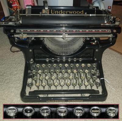
    The second type of tabulator was the tabulating typewriter (1890). These devices were simply typewriters with tab stops to make it easier to produce tables. (The "tabulating key" on these typewriters is is the root of the "tab" key on the modern computer keyboard.) The decimal tabulator (1896) added multiple tab keys that would tab to the proper location for a 1-digit number, 2-digit number, 3-digit number, etc.

    Underwood 6 typewriter with decimal tabulator (1934). Inset shows the decimal tab keys enlarged: "Tab Stop Clear", ".", "1", "10", "100", "1000", "Tab Stop Set". Interestingly, the platen scale shows 132 tick marks. Photo courtesy of J Makoto Smith.

    Underwood 6 typewriter with decimal tabulator (1934). Inset shows the decimal tab keys enlarged: "Tab Stop Clear", ".", "1", "10", "100", "1000", "Tab Stop Set". Interestingly, the platen scale shows 132 tick marks. Photo courtesy of J Makoto Smith.

    Later IBM punch card tabulators included a printer and printed tabular output, so they were tabulators in both senses. Soon afterward, IBM stopped calling them tabulators and changed the name to Electric Accounting Machine or EAM (1934). 

  7. In the 285 tabulator, the last type bar in a print bank often had an asterisk or "CR" symbol rather than numbers. An asterisk was used to indicate a subtotal, and "CR" indicated a credit (negative number). 

  8. Why did IBM's early punch cards have 45 columns with 5/32" spacing? See The Punched Card for history. The short answer is 28-column cards (from the 1890 census) used 1/8" holes with 1/8" between holes. The gap between holes was halved to 1/16" for 36-column cards, and halved again to 1/32" for 45-column cards, yielding 5/32" spacing. 

  9. IBM's early interpreters printed 45 columns of numeric-only data, on short 34-column cards, 45-column cards, or "modern" 80-column cards (details). (While 45-column cards were originally thought to have almost unlimited capacity to meet all requirements, the increase to 80 columns was soon necessary.) In the 1950s IBM introduced alphabetic interpreters that could print 60 columns of alphanumeric information on a punch card. The IBM 552 interpreter used 60 type bars. The IBM 557 interpreter (1954) switched to 60 typewheels. Apparently, the IBM 557 had reliability problems and later 60-column interpreters went back to type bars: the IBM 548 and IBM 552 (1958 and 1957). 

  10. The high quality of the IBM 1403's print was largely due to the use of a horizontally rotating chain. Earlier printers used type bars, type wheels, or drums. These approaches have the problem that any error in timing or positioning results in characters that are shifted vertically, resulting in objectionably wavy text. On the other hand, positioning errors with a type chain are horizontal, and people are much less sensitive to type that is spaced unevenly. 

  11. Why would customers care about standard form sizes? The 407 reference manual stated that forms of standard sizes can be obtained more quickly and economically from forms manufacturers than non-standard sizes. In addition, when using the pin-feed platen, the platen dimensions had to match to the form width. IBM had standard platens to match the standard form sizes (see 923 parts catalog page 16), but non-standard forms required a custom platen.  

  12. Accounting machines added support for continuous forms in several steps. On early tabulators, the operator needed to stop the machine and manually advance the paper to the top of each form. The IBM 921 Automatic Carriage (1935) provided a motorized mechanism to automatically jump to the top of a form or a particular position on the form. But even with an automatic carriage, the operator needed to ensure the forms didn't slip out of alignment (especially multiple-copy forms with carbon paper). Standard Register Co. solved this problem in 1931 with the pin-feed platen driving forms with feed holes along the edges. IBM tabulators supported these forms with a pin-feed platen or the IBM F-2 Forms Tractor (407 Manual p70). By 1936, Machine Methods of Accounting stated, "The use of continuous forms in business has been increasing at a rapid pace in recent years due to the perfection of more and better mechanical devices for handling such forms."  

  13. The standard form widths had a long lifetime, with most of them still available. The book Business Systems Handbook (1979) has a list of typical widths for continuous forms: 4 3/4", 5 3/4", 6 1/2", 8, 8 1/2", 9, 9 1/2", 9 7/8", 10 5/8", 11, 11 3/4", 12, 12 27/32", 13 5/8", 14 7/8", 15", 15 1/2", 16", 16 3/4", 17 25/32". (18 15/16" is the only standard IBM size missing from this list.) Even though IBM dropped many sizes in their 407 standard list (such as 12 27/32" and 17 25/32"), they were unsuccessful in killing off these sizes. 

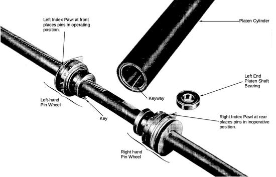
  14. A major part of my analysis is that the standard form hole-to-hole width is typically divisible by 5/32" (although not always). I couldn't find a stated reason for this, but I have a theory. To support continuous forms, pin wheel assemblies (below) are attached to the ends of the platen cylinder. Consequently, the hole-to-hole distance is determined by the platen width. It makes sense for the platen width to be a multiple of 5/32" so characters fit exactly. The distance from the edge of the platen to the pin centers appears to be 5/32". (I measured pixels in photos to determine this; I don't have solid proof.) Thus, the hole-to-hole distance will also be a multiple of 5/32"

    The pin-feed platen consists of two pin wheels that go on the end of the platen cylinder. Adapted from IBM Operators Reference Guide (1959) page 80.

    The pin-feed platen consists of two pin wheels that go on the end of the platen cylinder. Adapted from IBM Operators Reference Guide (1959) page 80.

    Many of the standard IBM form widths are divisible not only by the character width (5/32") but also divisible by the width of 4 characters (5/8"). I found a mention in Machine Methods of Accounting (page 17-1) that the IBM 405's original friction-feed carriage was adjustable in units of 4 characters, held in position by a notched rod. This suggests that these widths were easier to configure for mechanical reasons. 

  15. The IBM 285 tabulator was configured with 3 to 7 print banks, each 1 7/8" wide. (See Machine Methods of Accounting: Electric Tabulating Machines page 14.) I believe these were the source of the standard form widths 8", 9 7/8", 11 3/4", 13 5/8" and 15 1/2" (after adding some margin). Many of the other standard sizes are nice round numbers (e.g. 11" and 16"). 18 15/16" was probably selected to yield 18" paper (Arch B) with the punched margins (actually 1/16" smaller than 18" so the hole-to-hole width is a multiple of 5/32"). I can't come up with any plausible explanation for 17 25/32", but it may be related somehow to 17" ledger paper (ANSI B) or perhaps untrimmed paper sizes (SRA2, Demy).

    The 12 27/32" width was derived from loose-leaf accounting binders, which date back to 1896. In 1916, the Manufacturers of Loose Leaf Devices held a meeting in Atlantic City to establish standard sizes. They decided on 9 1/4"×11 7/8", 11 1/4"×11 7/8" and 7 1/2"×10 3/8". The standardization was successful since the smaller two sizes are still available today. To support the 11 7/8" ledgers, IBM apparently shaved off 1/32" to make the hole-to-hole width divisible by 5/32", yielding 11 27/32". Adding the 1/2" punched margins on each side results in the standard form width 12 27/32". While loose leaf may not seem exciting now, Office Appliances (1917) has a remarkable description of the victory of loose-leaf ledgers over "Prejudice, Indifference, Distrust" so they now "stand supreme as Leaders in modern progressiveness" in the "battle for Modern Efficiency". 

  16. Standardized tabulator form sizes were so prevalent that special business form rulers were produced to help design business forms. These rulers had markings indicating standard form widths and 5/32" and 0.1" scales for tabulator character spacing. These rulers are still available

  17. Since the 14 7/8" standardized width is very important, I'll discuss the math in more detail. The 405 accounting machine had 88 type bars, but there was one blank space (for a ribbon guide) between the alphanumeric and numeric type bars. Thus, the printing region was 89 × 5/32" = 13 29/32" wide. (As mentioned before, this just fits (probably by design) onto a 14" unperforated page.) Since standard perforated forms had 1/2" marginal perforations on each side to remove the holes, reasonable form widths would be 14 29/32" or 15". These values are not divisible (hole-to-hole) by 5/32"14. However, since the 402's characters have excessive white space around them, the characters still fit if we trim off 1/32" from the width. This yields a 13 7/8" line. Hole-to-hole, this is 14 3/8", divisible by 5/32" and even better 5/8". Adding the perforated margin, this yields 14 7/8" width as the "best" size to support the 405's 88-character output. (This seemed like random math, even to me, at first. But since the same approach explains the 12 27/32" width, I'm reasonably confident it's the right approach.) 

  18. Why did the 405 accounting machine (1934) and 402 accounting machine (1948) have 88 print positions? The accounting machines had a 43-column alphabetical print unit and a 45-column numeric-only print unit (below), with a 5/32" gap between for the ribbon. I think these type bar print units were derived from the 45-column type bar print unit used for the IBM 550 interpreter (1930), since they have the same 5/32" character spacing. But that raises the question of why two columns are missing from the alphabetical print unit. The 405's line of 88 characters with a gap between the units just fits onto a 14" page. (A 14" page without holes, friction-fed.) This is mentioned in Alphabetic Accounting Machines (1936) page 17-2, so it's presumably deliberate. So I think they used 88 columns instead of 90 in order to fit on 14" paper. 

  19. I talked to an old IBM engineer who serviced a company's collection of 407 tabulators as a new engineer, but after cleaning the type wheels he didn't put enough oil on them. A couple weeks later, the type wheels started seizing up and would hit the platen at high speed, sawing notches into the platen. (The platen is the roller that the paper goes around.) He used up IBM's entire East Coast collection of platens to fix these tabulators. He was afraid IBM would fire him over this, but they were supportive of engineers and he stayed for a long career. 

  20. The design of business forms was a complex task. The book Business Systems Handbook (1979) has a 30-page chapter discussing forms design, including how to meet customer needs, determining the size and layout of the form, and ideas on form techniques for various purposes. 

  21. In the 1970s, IBM still had 11 standard form widths, but there were a couple changes from the 407 era. An IBM patent mentions this in a vague way; apparently the 16 3/4" width was dropped and 11" added. 

  22. The diagram below gives some information on the dimensions of forms for the IBM 407 accounting machine.

    IBM's recommended specifications for forms. From Reference Manual, IBM 407 Accounting Machine.

    IBM's recommended specifications for forms. From Reference Manual, IBM 407 Accounting Machine.

    One important takeaway from this diagram is that the printing width is 1" less than the overall form width. It's interesting to note that the hole width is 5/32", exactly the same as the character width on a 402 accounting machine. 

  23. A width of 13 5/8" gives a printable region of 12 5/8". This fits 120 characters with 5/8" of extra space. A margin makes it easier to align the paper so characters fit between the perforations. Note that a margin is more important with 0.1" characters than 5/32" characters because the wider characters are already surrounded by white space. 

  24. Using 14 7/8" paper gives a printable region of 13 7/8" (13.875"), so you could fit 138 characters on a line. I couldn't find any 138-character printers, but several used 136-character lines. CDC in particular liked 136 columns, as shown by the CDC 501 line printer and later CDC 580. The book Print Unchained. said that 136 columns was a European width, but I haven't been able to find any line printer models fitting this. Later dot matrix printers from Epson, Datapro and other companies often supported 136 columns. 

  25. The timing of the 1403 printer is fairly complicated; I've made an animation here to illustrate it. The important thing for the current discussion is that every third character position gets a chance to print in sequence, so the printer makes three "subscans" to cover all the character positions. Thus, it makes sense for the line length to be a multiple of 3 so all the subscans are equal. Obviously it's possible for the 1403 printer to support a line length that isn't a multiple of 3, since some 1403 printer models supported 100-character lines. 

  26. This may be numerology, but it seems that IBM liked increasing print capacity in steps of 12. On the IBM 285 accounting machine, this made sense since each print bank was 12 characters wide. The IBM 407 accounting machine had 120 columns. The IBM 1443 printer (1962) had line lengths of 120 or 144 characters (2*12 characters more). So it seems plausible that the 132 column line was considered reasonable as it added one more 12-character column. 

  27. You might think that 128 characters per line would be more convenient since it's a power of 2. However, the IBM 1401 was a decimal (BCD) machine with decimal addressing. (For instance, it had 4000 characters of storage, not 4096.) Since it needed to count the line in decimal, there is no hardware advantage to 128. 

  28. To summarize the summary: 88 × 5/32" ≈ 132 × 0.1" (with a bit of margin) 

Hammer time: fixing the printer on a vintage IBM 1401 mainframe

The Computer History Museum has two operational IBM 1401 computers used for demos but one of the printers stopped working a few weeks ago. This blog post describes how the 1401 restoration team diagnosed and repaired the printer. After a lot of tricky debugging (as well as smoke coming out of the printer) we fixed a broken trace on a circuit board. (This printer repair might sound vaguely familiar because I wrote in September about an entirely different printer failure due to a failed transistor.)

The IBM 1401 business computer was announced in 1959, and went on to become the best-selling computer of the mid-1960s, with more than 10,000 systems in use. A key selling point of the IBM 1401 was its high-speed line printer, the IBM 1403. It printed 10 lines per second with excellent print quality, said to be the best printing until laser printers were introduced in the 1970s.

The IBM 1401 mainframe computer (left) at the Computer History Museum printing the Mandelbrot fractal on the 1403 printer (right).

The IBM 1401 mainframe computer (left) at the Computer History Museum printing the Mandelbrot fractal on the 1403 printer (right).

To print characters, the printer used a chain of type slugs (below) that rotated at high speed in front of the paper, with an inked ribbon between the paper and the chain. Each of the 132 print columns had a hammer and an electromagnet. At the right moment, when the desired character passed the hammer, an electromagnet drove the hammer against the back of the paper, causing the paper and ribbon to hit the type slug, printing the character.1

The type chain from the IBM 1401's printer. The chain has 48 different characters, repeated five times.

The type chain from the IBM 1401's printer. The chain has 48 different characters, repeated five times.

The printer required careful timing to make this process work. The chain spun around at 7.5 feet per second and each hammer had to fire at exactly the right time to print the right character perfectly aligned without smearing. Every 11.1 µs, a print slug lined up with a hammer, and the control circuitry checked if the slug matches the character to be printed. If so, the electromagnet was energized for 1.5 ms, printing the character.

Printing mechanism of the IBM 1401 line printer. From 1401 Reference Manual, p11.

Printing mechanism of the IBM 1401 line printer. From 1401 Reference Manual, p11.

While the printer is usually reliable, a few weeks ago the printer stopped working and displayed a "sync check" error on the console. The computer needs to know the exact position of the chain in order to fire the hammers at the right time. If something goes wrong with this synchronization, the computer stops with "sync check" rather than printing the wrong characters.

When the sync check light on the printer is illuminated, you have a problem.

When the sync check light on the printer is illuminated, you have a problem.

To track the chain position, the computer receives a sequence of pulses from the printer: a pulse when the first hammer is lined up with a type slug2 and a double pulse when the chain is in its "home" position with the first character lined up. The pulses are created by a slotted metallic timing disk inside the printer. A magnetic pickup detects these slots and produces a small 100 millivolt signal.7 This signal is amplified inside the printer by two differential amplifier cards to produce a stronger square wave signal. (This is the only electronic part of the printer. Everything else inside the printer is electromechanical or hydraulic; a high-speed hydraulic motor feeds paper through the printer and drips oil on the floor.)

The computer receives these pulses from the printer and generates a logic signal that increments counters to keep track of the chain's position. The schematic below shows part of the circuitry inside the computer, starting with the sense amplifier signal from the printer at the left. Don't try to understand this circuit; I just want to show the strange schematic symbols that IBM used in the 1960s. The box with "I" is an inverter. The triangle is an AND gate. The semicircle that looks like an AND gate is actually an OR gate. The large box with a "T" is a trigger, IBM's name for a flip-flop. The "SS" box is a "single shot" that creates a 400µs pulse; this detects the double pulse that indicates the chain's "home" position.

Excerpt from the 1401 Intermedia Level Diagrams (ILD) showing the chain detection circuitry.

Excerpt from the 1401 Intermedia Level Diagrams (ILD) showing the chain detection circuitry.

To track down the problem, we removed the printer's side panel to access the two amplifier circuit boards, which are visible below. We probed the boards with an oscilloscope. The first amplifier stage (on the right) looked okay, but the second stage (on the left) had problems. In the photo below, the computer is at the back, mostly hidden by the printer.

We took the side panel off the 1403 printer to reveal the circuit boards. We hooked an oscilloscope up to the front board to test it.

We took the side panel off the 1403 printer to reveal the circuit boards. We hooked an oscilloscope up to the front board to test it.

The trace below shows what should happen. The board receives a differential signal at the bottom, with alternating cyan and pink signals. The difference between these signals (middle) is amplified to produce the clean, uniform pulse train at the top. Note the double pulse in the middle indicating the chain's home position.

Oscilloscope trace from a working printer.

Oscilloscope trace from a working printer.

But when we measured the signal, we saw signals that were entirely garbled. The differential signals at the bottom are a mess, and track each other rather than alternating. The output signal (top) is basically random. With this signal from the printer, the computer couldn't keep track of the chain position and the sync check error resulted.

Oscilloscope trace from the faulty printer.

Oscilloscope trace from the faulty printer.

We swapped the board with the board from the other, working printer, and verified that the board was the problem. The museum has a filing cabinet full of replacement circuit boards, but unfortunately not a replacement for this "WW" amplifier board. Instead, we had to diagnose the problem with this card and repair it. On the board below you can see the diodes (small gray cylinders), capacitors (silver cylinders), resistors (striped cylinders and large tan cylinders), and germanium transistors (round metal cans). The transistors are germanium transistors as the 1401 predated silicon transistors.

The "WW" differential amplifier card used by the printer.

The "WW" differential amplifier card used by the printer.

We suspected a failed transistor, so we used Marc's vintage Hewlett-Packard Tektronix curve tracer (below) to test the transistors. One transistor was much weaker than the others. Since the performance of a differential amplifier depends on having transistors with closely matched characteristics, we searched through a couple dozen transistors to find a matching pair and replaced the transistors. (We later determined that these transistors were not part of the differential pair—they were "emitter follower" buffers, so our effort was wasted.)3

We used a vintage HP transistor curve tracer to test the transistors.

We used a vintage HP transistor curve tracer to test the transistors.

Back at the Computer History Museum, we tested out the repaired board and the printer still didn't work. Even worse, smoke started coming from the back of the printer! I quickly shut off the system as an acrid smell surrounded the printer. I expected to see a blackened transistor on the board, but it was fine. I examined the printer but couldn't find the source of the smoke.

I decided to test the board outside the printer by feeding in a 2kHz test signal, but the measurements didn't make sense. The board seemed to be ignoring one of the inputs, so I tested that input transistor but it was fine. Next I checked the diodes, capacitors and resistors again; all the components tested okay, but the board still mysteriously failed. I started carefully measuring voltages at various points in the circuit but the signals didn't make sense and weren't consistent. Since all the components were fine but the board didn't work, I was starting to losing confidence in electronics. Eventually, I nailed down a signal that randomly jumped between 10 volts and 1 volt. After wiggling all the components, I finally noticed that the voltage jumped if I flexed the board. Finally, I had an answer: a cracked trace on the circuit board between the input and the transistor was making intermittent contact.

The board had a cracked trace in the upper left, connecting the upper gold contact. Carl put a wire jumper across the bad section.

The board had a cracked trace in the upper left, connecting the upper gold contact. Carl put a wire jumper across the bad section.

To fix the board, Carl put a wire bridge across the bad trace6. We put the board in the printer, and the printer mostly worked. However, when the printer tried to print in column 85, the column failed to print and the printer stopped with an error.5 More testing revealed four columns of the printer were failing to print due to hammer problems. Each electromagnetic hammer coil is driven by a 60 volt, 5 amp pulse for 1.5 milliseconds. This is a lot of power (300 watts), so if anything goes wrong, hammer coils can easily burn up.

We swung open one of the computer's "gates" (lower left), revealing the cards that drive the printer.

We swung open one of the computer's "gates" (lower left), revealing the cards that drive the printer.

We looked at the printer driver cards inside the computer. Each card generates pulses for two hammers, so there are 66 of these cards. In the photo below, you can see the two large high-current transistors at the left that generate the pulses. (Note the felt insulators on top of these transistors. Due to their height, the transistors pose a risk of shorting against the bottom of the neighboring card.) Just to the right of these transistors are two colorful purple and yellow fuses. In the event of a fault, these fuses are supposed to burn out and protect the hammer coils. We checked the cards associated with the four bad columns on the printer and found four burnt-out fuses.

The "AEC" Alloy-Hammer Driver Latch card produces high-current pulses to drive the printer hammer coils.

The "AEC" Alloy-Hammer Driver Latch card produces high-current pulses to drive the printer hammer coils.

Why did the fuses blow? The circuit to drive the hammer coils is a bit tricky. Every 11 microseconds, a hammer lines up with a character slug and can be fired. But when a hammer is fired, the coil needs to be activated for about 1.5 ms, a much longer time interval. To accomplish this, the hammer driver latches on when a hammer is fired. Later in the print cycle, the hammer driver is turned off. This process is controlled by the chain position counters, which are driven by the pulses from the chain sensor, the same pulses that were intermittent. Thus, if the computer received enough pulses to start printing a line, but then the pulses dropped out in the middle of the line, hammer drivers could be left in the on state until the fuse blows. This explained the problem that we saw.

After Carl replaced the fuses, the printer worked fine except for two problems. First, characters in column 85 were shifted slightly so the text was slightly crooked. Frank explained that the hammer in this column must be moving a bit too slow, hitting the chain after it had moved past its position. This explained the smoke: in the time it took the fuse to blow, the coil must have overheated and been slightly damaged. We'll look into replacing this coil next week. The second problem was that the printer's Ready light didn't go on. This turned out to be simply a bad light bulb, unrelated to the rest of the problems. In any case, the printer was working well enough for demos so the repair was a success.

Closeup of the type chain (upside down) for an IBM 1403 line printer.

Closeup of the type chain (upside down) for an IBM 1403 line printer.

I announce my latest blog posts on Twitter, so follow me at @kenshirriff for future articles. I also have an RSS feed. The Computer History Museum in Mountain View runs demonstrations of the IBM 1401 on Wednesdays and Saturdays so if you're in the area you should definitely check it out (schedule).

Notes and references

  1. You might expect that the 132 hammers align with 132 type slugs, so the matching hammers all fire at once, but that's not what happens. Instead, the hammers and type slugs are spaced slightly differently, so only one hammer is aligned at a time, and a tiny movement of the chain lines up a different hammer and type slug. (Essentially they form a vernier.) Specifically, every 11.1 microseconds, the chain moves 0.001 inches. This causes a new hammer / type slug alignment. For mechanical reasons, every third hammer lines up in sequence (1, 4, 7, ...) until the end of the line is reached; this is called a "subscan" and takes 555 microseconds. Two more subscans give each hammer in the line an option to fire, forming a print scan of 1.665 milliseconds. If you want more information on how the print chain works, I have an animation here

  2. To be precise, the printer generates a pulse if hammer 1, 2, or 3 lines up with a type slug. This is due to the three "subscans", each using every third hammer. 

  3. I'll explain how the differential amplifier works in this footnote, since most readers may not want this much detail. The computer uses two differential amplifier boards in series, first a WV board and then a WW board. They use similar principles, except the WV uses NPN transistors and the WW uses PNP. The differential output from the WW board is transmitted to the computer where a third differential amplifier (an NT card) converts the signal to a logic output. Each board is a differential amplifier, which takes two inputs and amplifies the difference, essentially an op amp with two outputs.4

    A differential pair circuit.

    A differential pair circuit.

    The basic differential pair circuit for a differential amplifier is shown above. (Op amps contain a similar differential pair.) The resistor at the top sets a fixed current I. If the two inputs are equal, the current will be split, with half going through each transistor and branch resistor. But if one if the inputs is slightly lower, that transistor will conduct more and most of the current will go through that branch. Thus, the difference between the inputs steers the current down one side or the other, yielding an amplified signal across the lower resistors.

    Schematic of the WW amplifier board from the SMS documentation.

    Schematic of the WW amplifier board from the SMS documentation.

    The IBM 1401 documentation provides the schematic above for the board, but it's hard to follow what's happening. (Note the unusual transistor symbol, three boxes with an emitter arrow in or out.) I redrew the main part of the circuit below, so it resembles the simple differential pair. It has the same resistors at top and bottom as the differential pair, but there is an R-C circuit in each branch. To simplify, if there is a DC offset or low-frequency input, the capacitor will charge and counteract this offset. Thus, the amplifier operates as a high-pass amplifier; it cuts out low-frequency noise while amplifying the 1800 Hz sync pulses. The diodes clip the output, yielding a square wave. The differential output goes through emitter-follower buffers (omitted below) so the signal is strong enough to be transmitted through an under-floor cable from the printer to the computer.

    The differential amplifier circuit of the WW card.

    The differential amplifier circuit of the WW card.


  4. An op amp with positive and negative outputs is known as a "fully differential op amp". 

  5. The IBM 1403 printer has multiple error checks to avoid printing incorrect data. For a business machine, it would be bad to drop digits in, say, payroll checks or tax records. To detect hammer failures, the printer has 132 wires from the hammers back to the computer, to verify that each hammer fired when it was supposed to. If the computer doesn't get a pulse back from a hammer, the computer stops immediately, as we saw. 

  6. We noticed that there was solder smeared across the broken part of the trace. My suspicion is that the same problem happened a few years ago and was repaired by bridging the broken trace with solder. Eventually the heavy vibrations inside the printer caused a hairline crack in the solder, causing the problem to recur. By bridging the break with wire rather than just solder, we hope we have fixed the problem permanently. We also noticed the transistor connected to the broken trace had been replaced, so they must have tried that first in the previous repair. 

  7. The 1403 printer is documented in IBM 1403 Printer Component Description and 1403 Printers Field Engineering Maintenance Manual. See also this brief article about the 1403 printer in the IEEE Spectrum. For details on how the timing pulses work, see the 1403 Manual of Instruction, page 42. 

Two bits per transistor: high-density ROM in Intel's 8087 floating point chip

The 8087 chip provided fast floating point arithmetic for the original IBM PC and became part of the x86 architecture used today. One unusual feature of the 8087 is it contained a multi-level ROM (Read-Only Memory) that stored two bits per transistor, twice as dense as a normal ROM. Instead of storing binary data, each cell in the 8087's ROM stored one of four different values, which were then decoded into two bits. Because the 8087 required a large ROM for microcode1 and the chip was pushing the limits of how many transistors could fit on a chip, Intel used this special technique to make the ROM fit. In this article, I explain how Intel implemented this multi-level ROM.

Intel introduced the 8087 chip in 1980 to improve floating-point performance on the 8086 and 8088 processors. Since early microprocessors operated only on integers, arithmetic with floating point numbers was slow and transcendental operations such as trig or logarithms were even worse. Adding the 8087 co-processor chip to a system made floating point operations up to 100 times faster. The 8087's architecture became part of later Intel processors, and the 8087's instructions (although now obsolete) are still a part of today's x86 desktop computers.

I opened up an 8087 chip and took die photos with a microscope yielding the composite photo below. The labels show the main functional blocks, based on my reverse engineering. (Click here for a larger image.) The die of the 8087 is complex, with 40,000 transistors.2 Internally, the 8087 uses 80-bit floating point numbers with a 64-bit fraction (also called significand or mantissa), a 15-bit exponent and a sign bit. (For a base-10 analogy, in the number 6.02x10²³, 6.02 is the fraction and 23 is the exponent.) At the bottom of the die, "fraction processing" indicates the circuitry for the fraction: from left to right, this includes storage of constants, a 64-bit shifter, the 64-bit adder/subtracter, and the register stack. Above this is the circuitry to process the exponent.

Die of the Intel 8087 floating point unit chip, with main functional blocks labeled.

Die of the Intel 8087 floating point unit chip, with main functional blocks labeled.

An 8087 instruction required multiple steps, over 1000 in some cases. The 8087 used microcode to specify the low-level operations at each step: the shifts, adds, memory fetches, reads of constants, and so forth. You can think of microcode as a simple program, written in micro-instructions, where each micro-instruction generated control signals for the different components of the chip. In the die photo above, you can see the ROM that holds the 8087's microcode program. The ROM takes up a large fraction of the chip, showing why the compact multi-level ROM was necessary. To the left of the ROM is the "engine" that ran the microcode program, essentially a simple CPU.

The 8087 operated as a co-processor with the 8086 processor. When the 8086 encountered a special floating point instruction, the processor ignored it and let the 8087 execute the instruction in parallel.3 I won't explain in detail how the 8087 works internally, but as an overview, floating point operations were implemented using integer adds/subtracts and shifts. To add or subtract two floating point numbers, the 8087 shifted the numbers until the binary points (i.e. the decimal points but in binary) lined up, and then added or subtracted the fraction. Multiplication, division, and square root were performed through repeated shifts and adds or subtracts. Transcendental operations (tan, arctan, log, power) used CORDIC algorithms, which use shifts and adds of special constants, processing one bit at a time. The 8087 also dealt with many special cases: infinities, overflows, NaN (not a number), denormalized numbers, and several rounding modes. The microcode stored in ROM controlled all these operations.

Implementation of a ROM

The 8087 chip consists of a tiny silicon die, with regions of the silicon doped with impurities to give them the desired semiconductor properties. On top of the silicon, polysilicon (a special type of silicon) formed wires and transistors. Finally, a metal layer on top wired the circuitry together. In the photo below, the left side shows a small part of the chip as it appears under a microscope, magnifying the yellowish metal wiring. On the right, the metal has been removed with acid, revealing the polysilicon and silicon. When polysilicon crosses silicon, a transistor is formed. The pink regions are doped silicon, and the thin vertical lines are the polysilicon. The small circles are contacts between the silicon and metal layers, connecting them together.

Structure of the ROM in the Intel 8087 FPU. The metal layer is on the left and the polysilicon and silicon layers are on the right.

Structure of the ROM in the Intel 8087 FPU. The metal layer is on the left and the polysilicon and silicon layers are on the right.

While there are many ways of building a ROM, a typical way is to have a grid of "cells," with each cell holding a bit. Each cell can have a transistor for a 0 bit, or lack a transistor for a 1 bit. In the diagram above, you can see the grid of cells with transistors (where silicon is present under the polysilicon) and missing transistors (where there are gaps in the silicon). To read from the ROM, one column select line is energized (based on the address) to select the bits stored in that column, yielding one output bit from each row. You can see the vertical polysilicon column select lines and the horizontal metal row outputs in the diagram. The vertical doped silicon lines are connected to ground.

The schematic below (corresponding to a 4×4 ROM segment) shows how the ROM functions. Each cell either has a transistor (black) or no transistor (grayed-out). When a polysilicon column select line is energized, the transistors in that column turn on and pull the corresponding metal row outputs to ground. (For our purposes, an NMOS transistor is like a switch that is open if the input (gate) is 0 and closed if the input is 1.) The row lines output the data stored in the selected column.

Schematic of a 4×4 segment of a ROM.

Schematic of a 4×4 segment of a ROM.

The column select signals are generated by a decoder circuit. Since this circuit is built from NOR gates, I'll first explain the construction of a NOR gate. The schematic below shows a four-input NOR gate built from four transistors and a pull-up resistor (actually a special transistor). On the left, all inputs are 0 so all the transistors are off and the pull-up resistor pulls the output high. On the right, an input is 1, turning on a transistor. The transistor is connected to ground, so it pulls the output low. In summary, if any inputs are high, the output is low so this circuit implements a NOR gate.

4-input NOR gate constructed from NMOS transistors.

4-input NOR gate constructed from NMOS transistors.

The column select decoder circuit takes the incoming address bits and activates the appropriate select line. The decoder contains an 8-input NOR gate for each column, with one NOR gate selected for the desired address. The photo shows two of the NOR gates generating two of the column select signals. (For simplicity, I only show four of the 8 inputs). Each column uses a different combination of address lines and complemented address lines as inputs, selecting a different address. The address lines are in the metal layer, which was removed for the photo below; the address lines are drawn in green. To determine the address associated with a column, look at the square contacts associated with each transistor and note which address lines are connected. If all the address lines connected to a column's transistors are low, the NOR gate will select the column.

Part of the address decoder. The address decoder selects odd columns in the ROM, counting right to left. The numbers at the top show the address associated with each output.

Part of the address decoder. The address decoder selects odd columns in the ROM, counting right to left. The numbers at the top show the address associated with each output.

The photo below shows a small part of the ROM's decoder with all 8 inputs to the NOR gates. You can read out the binary addresses by carefully examining the address line connections. Note the binary pattern: a1 connections alternate every column, a2 connections alternate every two columns, a3 connections every four columns, and so forth. The a0 connection is fixed because this decoder circuit selects the odd columns; a similar circuit above the ROM selects the even addresses. (This split was necessary to make the decoder fit on the chip because each decoder column is twice as wide as a ROM cell.)

Part of the address decoder for the 8087's microcode ROM. The decoder converts an 8-bit address into column select signals.

Part of the address decoder for the 8087's microcode ROM. The decoder converts an 8-bit address into column select signals.

The last component of the ROM is the set of multiplexers that reduces the 64 output rows down to 8 rows.4 Each 8-to-1 multiplexer selects one of its 8 inputs, based on the address. The diagram below shows one of these row multiplexers in the 8087, built from eight large pass transistors, each one connected to one of the row lines. All the transistors are connected to the output so when the selected transistor is turned on, it passes its input to the output. The multiplexer transistors are much, much larger than the transistors in the ROM to reduce distortion of the ROM signal. A decoder (similar to the one discussed earlier, but smaller) generates the eight multiplexer control lines from three address lines.

One of eight row multiplexers in the ROM. This shows the poly/silicon layers, with metal wiring drawn in orange.

One of eight row multiplexers in the ROM. This shows the poly/silicon layers, with metal wiring drawn in orange.

To summarize, the ROM stores bits in a grid. It uses eight address bits to select a column in the grid. Then three address bits select the desired eight outputs from the row lines.

The multi-level ROM

The discussion so far explained of a typical ROM that stores one bit per cell. So how did 8087 store two bits per cell? If you look closely, the 8087's microcode ROM has four different transistor sizes (if you count "no transistor" as a size).6 With four possibilities for each transistor, a cell can encode two bits, approximately doubling the density.7 This section explains how the four transistor sizes generate four different currents, and how the chip's analog and digital circuitry converts these currents into two bits.

A closeup of the 8087's microcode ROM shows four different transistor sizes. This allows the ROM to store two bits per cell.

A closeup of the 8087's microcode ROM shows four different transistor sizes. This allows the ROM to store two bits per cell.

The size of the transistor controls the current through the transistor.8 The important geometric factor is the varying width of the silicon (pink) where it is crossed by the polysilicon (vertical lines), creating transistors with different gate widths. Since the gate width controls the current through the transistor, the four transistor sizes generate four different currents: the largest transistor passes the most current and no current will flow if there is no transistor at all.

The ROM current is converted to bits in several steps. First, a pull-up resistor converts the current to a voltage. Next, three comparators compare the voltage with reference voltages to generate digital signals indicating if the ROM voltage is lower or higher. Finally, logic gates convert the comparator output signals to the two output bits. This circuitry is repeated eight times, generating 16 output bits in total.

The circuit to read two bits from a ROM cell.

The circuit to read two bits from a ROM cell.

The circuit above performs these conversion steps. At the bottom, one of the ROM transistors is selected by the column select line and the multiplexer (discussed earlier), generating one of four currents. Next, a pull-up resistor12 converts the transistor's current to a voltage, resulting in a voltage depending on the size of the selected transistor. The comparators compare this voltage to three reference voltages, outputting a 1 if the ROM voltage is higher than the reference voltage. The comparators and reference voltages require careful design because the ROM voltages could differ by as little as 200 mV.

The reference voltages are mid-way between the expected ROM voltages, allowing some fluctuation in the voltages. The lowest ROM voltage is lower than all the reference voltages so all comparators will output 0. The second ROM voltage is higher than Reference 0, so the bottom comparator outputs 1. For the third ROM voltage, the bottom two comparators output 1, and for the highest ROM voltage all comparators output 1. Thus, the three comparators yield four different output patterns depending on the ROM transistor. The logic gates then convert the comparator outputs into the two output bits.10

The design of the comparator is interesting because it is the bridge between the analog and digital worlds, producing a 1 or 0 if the ROM voltage is higher or lower than the reference voltage. Each comparator contains a differential amplifier that amplifies the difference between the ROM voltage and the reference voltage. The output from the differential amplifier drives a latch that stabilizes the output and converts it to a logic-level signal. The differential amplifier (below) is a standard analog circuit. A current sink (symbol at the bottom) provides a constant current. If one of the transistors has a higher input voltage than the other, most of the current passes through that transistor. The voltage drop across the resistors will cause the corresponding output to go lower and the other output to go higher.

Diagram showing the operation of a differential pair. Most of the current will flow through the transistor with the higher input voltage, pulling the corresponding output lower. The double-circle symbol at the bottom is a current sink, providing a constant current I.

Diagram showing the operation of a differential pair. Most of the current will flow through the transistor with the higher input voltage, pulling the corresponding output lower. The double-circle symbol at the bottom is a current sink, providing a constant current I.

The photo below shows one of the comparators on the chip; the metal layer is on top, with the transistors underneath. I'll just discuss the highlights of this complex circuit; see the footnote12 for details. The signal from the ROM and multiplexer enters on the left. The pull-up circuit12 converts the current into a voltage. The two large transistors of the differential amplifier compare the ROM's voltage with the reference voltage (entering at top). The outputs from the differential amplifier go to the latch circuitry (spread across the photo); the latch's output is in the lower right. The differential amplifier's current source and pull-up resistors are implemented with depletion-mode transistors. Each output circuit uses three comparators, yielding 24 comparators in total.

One of the comparators in the 8087. The chip contains 24 comparators to convert the voltage levels from the multi-level ROM into binary data.

One of the comparators in the 8087. The chip contains 24 comparators to convert the voltage levels from the multi-level ROM into binary data.

Each reference voltage is generated by a carefully-sized transistor and a pull-up circuit. The reference voltage circuit is designed as similar as possible to the ROM's signal circuitry, so any manufacturing variations in the chip will affect both equally. The reference voltage and ROM signal both use the same pull-up circuit. In addition, each reference voltage circuit includes a very large transistor identical to the multiplexer transistor, even though there is no multiplexing in the reference circuit, just to make the circuits match. The three reference voltage circuits are identical except for the size of the reference transistor.9

Circuit generating the three reference voltages. The reference transistors are sized between the ROM's transistor sizes. The oxide layer wasn't fully removed from this part of the die, causing the color swirls in the photo.

Circuit generating the three reference voltages. The reference transistors are sized between the ROM's transistor sizes. The oxide layer wasn't fully removed from this part of the die, causing the color swirls in the photo.

Putting all the pieces together, the photo below shows the layout of the microcode ROM components on the chip.12 The bulk of the ROM circuitry is the transistors holding the data. The column decoder circuitry is above and below this. (Half the column select decoders are at the top and half are at the bottom so they fit better.) The output circuitry is on the right. The eight multiplexers reduce the 64 row lines down to eight. The eight rows then go into the comparators, generating the 16 output bits from the ROM at the right. The reference circuit above the comparators generates the three reference voltage. At the bottom right, the small row decoder controls the multiplexers.

Microcode ROM from the Intel 8087 FPU with main components labeled.

Microcode ROM from the Intel 8087 FPU with main components labeled.

While you'd hope for the multi-level ROM to be half the size of a regular ROM, it isn't quite that efficient because of the extra circuitry for the comparators and because the transistors were slightly larger to accommodate the multiple sizes. Even so, the multi-level ROM saved about 40% of the space a regular ROM would have taken.

Now that I have determined the structure of the ROM, I could read out the contents of the ROM simply (but tediously) by looking at the size of each transistor under a microscope. But without knowing the microcode instruction set, the ROM contents aren't useful.

Conclusions

The 8087 floating point chip used an interesting two-bit-per-cell structure to fit the microcode onto the chip. Intel re-used the multi-level ROM structure in 1981 in the doomed iAPX 432 system.11 As far as I can tell, interest in ROMs with multiple-level cells peaked in the 1980s and then died out, probably because Moore's law made it easier to gain ROM capacity by shrinking a standard ROM cell rather than designing non-standard ROMs requiring special analog circuits built to high tolerances.14

Surprisingly, the multi-level concept has recently returned, but this time in flash memory. Many flash memories store two or more bits per cell.13 Flash has even achieved a remarkable 4 bits per cell (requiring 16 different voltage levels) with "quad-level cell" consumer products announced recently. Thus, an obscure technology from the 1980s can show up again decades later.

I announce my latest blog posts on Twitter, so follow me at @kenshirriff for future 8087 articles. I also have an RSS feed. Thanks to Jeff Epler for suggesting that I investigate the 8087's ROM.

Notes and references

  1. The 8087 has 1648 words of microcode (if I counted correctly), with 16 bits in each word, for a total of 26368 bits. The ROM size didn't need to be a power of two since Intel could build it to the exact size required. 

  2. Sources provide inconsistent values for the number of transistors in the 8087: Intel claims 40,000 transistors while Wikipedia claims 45,000. The discrepancy could be due to different ways of counting transistors. In particular, since the number of transistors in a ROM, PLA or similar structure depends on the data stored in it, sources often count "potential" transistors rather than the number of physical transistors. Other discrepancies can be due to whether or not pull-up transistors are counted and if high-current drivers are counted as multiple transistors in parallel or one large transistor. 

  3. The interaction between the 8086 processor and the 8087 floating point unit is somewhat tricky; I'll discuss some highlights. The simplified view is that the 8087 watches the 8086's instruction stream, and executes any instructions that are 8087 instructions. The complication is that the 8086 has an instruction prefetch buffer, so the instruction being fetched isn't the one being executed. Thus, the 8087 duplicates the 8086's prefetch buffer (or the 8088's smaller prefetch buffer), so it knows that the 8086 is doing. Another complication is the complex addressing modes used by the 8086, which use registers inside the 8086. The 8087 can't perform these addressing modes since it doesn't have access to the 8086 registers. Instead, when the 8086 sees an 8087 instruction, it does a memory fetch from the addressed location and ignores the result. Meanwhile, the 8087 grabs the address off the bus so it can use the address if it needs it. If there is no 8087 present, you might expect a trap, but that's not what happens. Instead, for a system without an 8087, the linker rewrites the 8087 instructions, replacing them with subroutine calls to the emulation library. 

  4. The reason ROMs typically use multiplexers on the row outputs is that it is inefficient to make a ROM with many columns and just a few output bits, because the decoder circuitry will be bigger than the ROM's data. The solution is to reshape the ROM, to hold the same bits but with more rows and fewer columns. For instance, the ROM can have 8 times as many rows and 1/8 the columns, making the decoder 1/8 the size.

    In addition, a long, skinny ROM (e.g. 1K×16) is inconvenient to lay out on a chip, since it won't fit as a simple block. However, a serpentine layout could be used. For example, Intel's early memories were shift registers; the 1405 held 512 bits in a single long shift register. To fit this onto a chip, the shift register wound back and forth about 20 times (details). 

  5. Some IBM computers used an unusual storage technique to hold microcode: Mylar cards had holes punched in them (just like regular punch cards), and the computer sensed the holes capacitively (link). Some computers, such as the Xerox Alto, had some microcode in RAM. This allowed programs to modify the microcode, creating a new instruction set for their specific purposes. Many modern processors have writeable microcode so patches can fix bugs in the microcode. 

  6. I didn't notice the four transistor sizes in the microcode ROM until a comment on Hacker News mentioned that the 8087 used two-bit-per-cell technology. I was skeptical, but after looking at the chip more closely I realized the comment was correct. 

  7. Several other approaches were used in the 1980s to store multiple bits per cell. One of the most common was used by Mostek and other companies: transistors in the ROM were doped to have different threshold voltages. By using four different threshold voltages, two bits could be stored per cell. Compared to Intel's geometric approach, the threshold approach was denser (since all the transistors could be as small as possible), but required more mask layers and processing steps to produce the multiple implantation levels. This approach used the new (at the time) technology of ion implantation to carefully tune the doping levels of each transistor.

    Ion implantation's biggest impact on integrated circuits was its use to create depletion transistors (transistors with a negative threshold voltage), which worked much better as pull-up resistors in logic gates. Ion implantation was also used in the Z-80 microprocessor to create some transistor "traps", circuits that looked like regular transistors under a microscope but received doping implants that made them non-functional. This served as copy protection since a manufacturer that tried to produce clones on the Z-80 by copying the chip with a microscope would end up with a chip that failed in multiple ways, some of them very subtle. 

  8. The current through the transistor is proportional to the ratio between the width and length of the gate. (The length is the distance between the source and drain.) The ROM transistors (and all but the smallest reference transistor) keep the length constant and modify the width, so shrinking the width reduces the current flow. For MOSFET equations, see Wikipedia

  9. The gate of the smallest reference transistor is made longer rather than narrower, due to the properties of MOS transistors. The problem is that the reference transistors need to have sizes between the sizes of the ROM transistors. In particular, Reference 0 needs a transistor smaller than the smallest ROM transistor. But the smallest ROM transistor is already as small as possible using the manufacturing techniques. To solve this, note that the polysilicon crossing the middle reference transistor is much thicker horizontally. Since a MOS transistor's properties are determined by the width to height ratio of its gate, expanding the polysilicon is as good as shrinking the silicon for making the transistor act smaller (i.e. lower current). 

  10. The ROM logic decodes the transistor size to bits as follows: No transistor = 00, small transistor = 01, medium transistor = 11, large transistor = 10. This bit ordering saves a few gates in the decoding logic; since the mapping from transistor to bits is arbitrary, it doesn't matter that the sequence is not in order. (See "Two Bits Per Cell ROM", Stark for details.)  

  11. Intel's iAPX 43203 interface processor (1981) used a multiple-level ROM very similar to the one in the 8087 chip. For details, see "The interface processor for the Intel VLSI 432 32 bit computer," J. Bayliss et al., IEEE J. Solid-State Circuits, vol. SC-16, pp. 522-530, Oct. 1981.
    The 43203 interface processor provided I/O support for the iAPX 432 processor. Intel started the iAPX 432 project in 1975 to produce a "micromainframe" that would be Intel's revolutionary processor for the 1980s. When the iAPX 432 project encountered delays, Intel produced the 8086 processor as a stopgap, releasing it in 1978. While the Intel 8086 was a huge success, leading to the desktop PC and the current x86 architecture, the iAPX 432 project ended up a failure and ended in 1986. 

  12. The schematic below (from "Multiple-Valued ROM Output Circuits") provides details of the circuitry to read the ROM. Conceptually the ROM uses a pull-up resistor to convert the transistor's current to a voltage. The circuit actually uses a three transistor circuit (T3, T4, T5) as the pull-up. T4 and T5 are essentially an inverter providing negative feedback via T3, making the circuit less sensitive to perturbations (such as manufacturing variations). The comparator consists of a simple differential amplifier (yellow) with T6 acting as the current source. The differential amplifier output is converted into a stable logic-level signal by the latch (green).

    Diagram of 8087 ROM output circuit.

    Diagram of 8087 ROM output circuit.

  13. Flash memories are categorized as SLC (single level cell—one bit per cell), MLC (multi level cell—two bits per cell), TLC (triple level cell—three bits per cell) and QLC (quad level cell—four bits per cell). In general, flash with more bits per cell is cheaper but less reliable, slower, and wears out faster due to the smaller signal margins. 

  14. The journal Electronics published a short article "Four-State Cell Doubles ROM Bit Capacity" (p39, Oct 9, 1980), describing Intel's technique, but the article is vague to the point of being misleading. Intel published a detailed article "Two bits per cell ROM" in COMPCON (pp209-212, Feb 1981). An external group attempted to reverse engineer more detailed specifications of the Intel circuits in "Multiple-valued ROM output circuits" (Proc. 14th Int. Symp. Multivalue Logic, 1984). Two papers describing multiple-value memories are A Survey of Multivalued Memories (IEEE Transactions on Computers, Feb 1986, pp 99-106) and A review of multiple-valued memory technology (IEEE Symposium on Multiple-Valued Logic, 1998).