Showing posts sorted by relevance for query i960. Sort by date Show all posts

The complex history of the Intel i960 RISC processor

The Intel i960 was a remarkable 32-bit processor of the 1990s with a confusing set of versions. Although it is now mostly forgotten (outside the many people who used it as an embedded processor), it has a complex history. It had a shot at being Intel's flagship processor until x86 overshadowed it. Later, it was the world's best-selling RISC processor. One variant was a 33-bit processor with a decidedly non-RISC object-oriented instruction set; it became a military standard and was used in the F-22 fighter plane. Another version powered Intel's short-lived Unix servers. In this blog post, I'll take a look at the history of the i960, explain its different variants, and examine silicon dies. This chip has a lot of mythology and confusion (especially on Wikipedia), so I'll try to clear things up.

Roots: the iAPX 432

"Intel 432": Cover detail from Introduction to the iAPX 432 Architecture.

"Intel 432": Cover detail from Introduction to the iAPX 432 Architecture.

The ancestry of the i960 starts in 1975, when Intel set out to design a "micro-mainframe", a revolutionary processor that would bring the power of mainframe computers to microprocessors. This project, eventually called the iAPX 432, was a huge leap in features and complexity. Intel had just released the popular 8080 processor in 1974, an 8-bit processor that kicked off the hobbyist computer era with computers such as the Altair and IMSAI. However, 8-bit microprocessors were toys compared to 16-bit minicomputers like the PDP-11, let alone mainframes like the 32-bit IBM System/370. Most companies were gradually taking minicomputer and mainframe features and putting them into microprocessors, but Intel wanted to leapfrog to a mainframe-class 32-bit processor. The processor would make programmers much more productive by bridging the "semantic gap" between high-level languages and simple processors, implementing many features directly into the processor.

The 432 processor included memory management, process management, and interprocess communication. These features were traditionally part of the operating system, but Intel built them in the processor, calling this the "Silicon Operating System". The processor was also one of the first to implement the new IEEE 754 floating-point standard, still in use by most processors. The 432 also had support for fault tolerance and multi-processor systems. One of the most unusual features of the 432 was that instructions weren't byte aligned. Instead, instructions were between 6 and 321 bits long, and you could jump into the middle of a byte. Another unusual feature was that the 432 was a stack-based machine, pushing and popping values on an in-memory stack, rather than using general-purpose registers.

The 432 provided hardware support for object-oriented programming, built around an unforgeable object pointer called an Access Descriptor. Almost every structure in a 432 program and in the system itself is a separate object. The processor provided fine-grain security and access control by checking every object access to ensure that the user had permission and was not exceeding the bounds of the object. This made buffer overruns and related classes of bugs impossible, unlike modern processors.

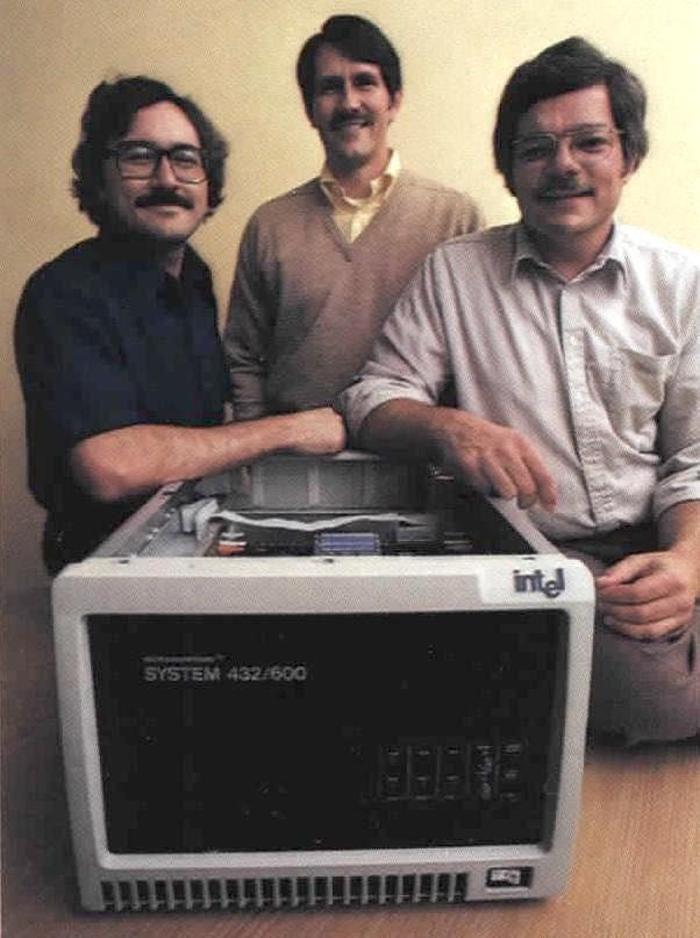
This photo from the Intel 1981 annual report shows Intel's 432-based development computer and three of the engineers.

This photo from the Intel 1981 annual report shows Intel's 432-based development computer and three of the engineers.

The new, object-oriented Ada language was the primary programming language for the 432. The US Department of Defense developed the Ada language in the late 1970s and early 1980s to provide a common language for embedded systems, using the latest ideas from object-oriented programming. Proponents expected Ada to become the dominant computer language for the 1980s and beyond. In 1979, Intel realized that Ada was a good target for the iAPX 432, since they had similar object and task models. Intel decided to "establish itself as an early center of Ada technology by using the language as the primary development and application language for the new iAPX 432 architecture." The iAPX 432's operating system (iMAX 432) and other software were written in Ada, using one of the first Ada compilers.

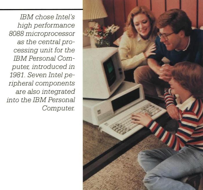
Unfortunately, iAPX 432 project was way too ambitious for its time. After a couple of years of slow progress, Intel realized that they needed a stopgap processor to counter competitors such as Zilog and Motorola. Intel quickly designed a 16-bit processor that they could sell until the 432 was ready. This processor was the Intel 8086 (1978), which lives on in the x86 architecture used by most computers today. Critically, the importance of the 8086 was not recognized at the time. In 1981, IBM selected Intel's 8088 processor (a version of the 8086 with an 8-bit bus) for the IBM PC. In time, the success of the IBM PC and compatible systems led to Intel's dominance of the microprocessor market, but in 1981 Intel viewed the IBM PC as just another design win. As Intel VP Bill Davidow later said, "We knew it was an important win. We didn't realize it was the only win."

Caption: IBM chose Intel's high performance 8088 microprocessor as the central processing unit for the IBM Personal Computer, introduced in 1981. Seven Intel peripheral components are also integrated into the IBM Personal Computer.  From Intel's 1981 annual report.

Caption: IBM chose Intel's high performance 8088 microprocessor as the central processing unit for the IBM Personal Computer, introduced in 1981. Seven Intel peripheral components are also integrated into the IBM Personal Computer. From Intel's 1981 annual report.

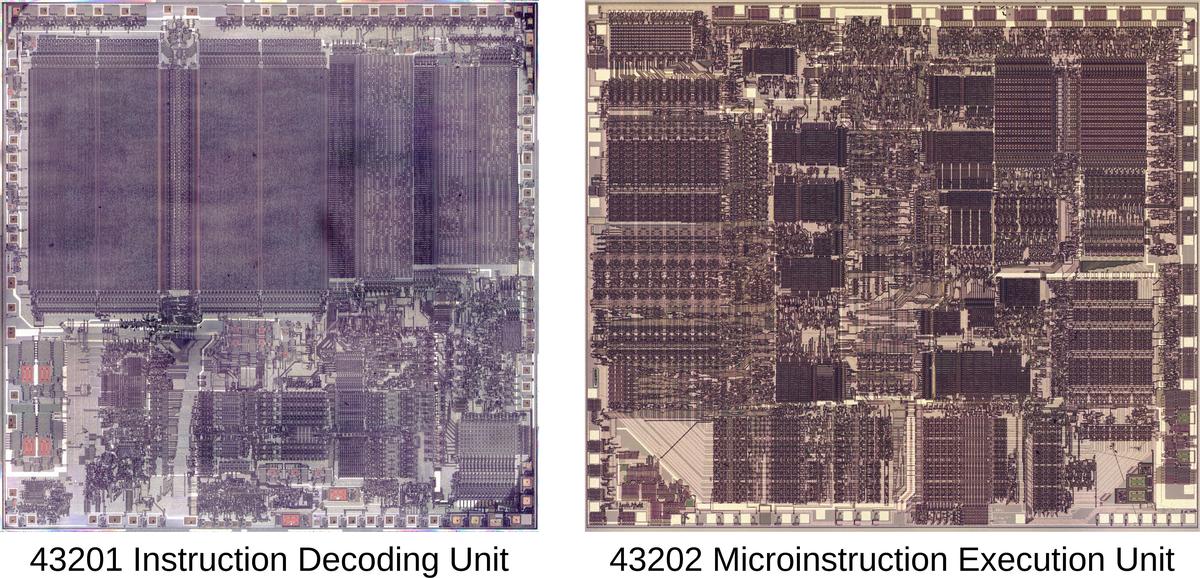
Intel finally released the iAPX 432 in 1981. Intel's 1981 annual report shows the importance of the 432 to Intel. A section titled "The Micromainframe™ Arrives" enthusiastically described the iAPX 432 and how it would "open the door to applications not previously feasible". To Intel's surprise, the iAPX 432 ended up as "one of the great disaster stories of modern computing" as the New York Times put it. The processor was so complicated that it was split across two very large chips:1 one to decode instructions and a second to execute them Delivered years behind schedule, the micro-mainframe's performance was dismal, much worse than competitors and even the stopgap 8086.2 Sales were minimal and the 432 quietly dropped out of sight.

My die photos of the two chips that make up the iAPX 432 General Data Processor. Click for a larger version.

My die photos of the two chips that make up the iAPX 432 General Data Processor. Click for a larger version.

Intel picks a 32-bit architecture (or two, or three)

In 1982, Intel still didn't realize the importance of the x86 architecture. The follow-on 186 and 286 processors were released but without much success at first.3 Intel was working on the 386, a 32-bit successor to the 286, but their main customer IBM was very unenthusiastic.4 Support for the 386 was so weak that the 386 team worried that the project might be dead.5 Meanwhile, the 432 team continued their work. Intel also had a third processor design in the works, a 32-bit VAX-like processor codenamed P4.6

Intel recognized that developing three unrelated 32-bit processors was impractical and formed a task force to develop a Single High-End Architecture (SHEA). The task force didn't achieve a single architecture, but they decided to merge the 432 and the P4 into a processor codenamed the P7, which would become the i960. They also decided to continue the 386 project. (Ironically, in 1986, Intel started yet another 32-bit processor, the unrelated i860, bringing the number of 32-bit architectures back to three.)

At the time, the 386 team felt that they were treated as the "stepchild" while the P7 project was the focus of Intel's attention. This would change as the sales of x86-based personal computers climbed and money poured into Intel. The 386 team would soon transform from stepchild to king.5

The first release of the i960 processor

Meanwhile, the 1980 paper The case for the Reduced Instruction Set Computer proposed a revolutionary new approach for computer architecture: building Reduced Instruction Set Computers (RISC) instead of Complex Instruction Set Computers (CISC). The paper argued that the trend toward increasing complexity was doing more harm than good. Instead, since "every transistor is precious" on a VLSI chip, the instruction set should be simplified, only adding features that quantitatively improved performance.

The RISC approach became very popular in the 1980s. Processors that followed the RISC philosophy generally converged on an approach with 32-bit easy-to-decode instructions, a load-store architecture (separating computation instructions from instructions that accessed memory), straightforward instructions that executed in one clock cycle, and implementing instructions directly rather than through microcode.

The P7 project combined the RISC philosophy and the ideas from the 432 to create Intel's first RISC chip, originally called the 809607 and later the i960. The chip, announced in 1988, was significant enough for coverage in the New York Times. Analysts said that the chip was marketed as an embedded controller to avoid stealing sales from the 80386. However, Intel's claimed motivation was the size of the embedded market; Intel chip designer Steve McGeady said at the time, "I'd rather put an 80960 in every antiskid braking system than in every Sun workstation.” Nonetheless, Intel also used the i960 as a workstation processor, as will be described in the next section.

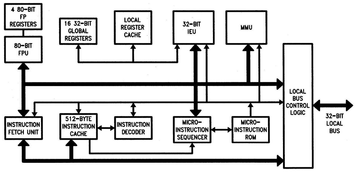
The block diagram below shows the microarchitecture of the original i960 processors. The microarchitecture of the i960 followed most (but not all) of the common RISC design: a large register set, mostly one-cycle instructions, a load/store architecture, simple instruction formats, and a pipelined architecture. The Local Register Cache contains four sets of the 16 local registers. These "register windows" allow the registers to be switched during function calls without the delay of saving registers to the stack. The micro-instruction ROM and sequencer hold microcode for complex instructions; microcode is highly unusual for a RISC processor. The chip's Floating Point Unit8 and Memory Management Unit are advanced features for the time.

The microarchitecture of the i960 XA. FPU is Floating Point Unit. IEU is Instruction Execution Unit. MMU is Memory Management Unit. From the 80960 datasheet.

The microarchitecture of the i960 XA. FPU is Floating Point Unit. IEU is Instruction Execution Unit. MMU is Memory Management Unit. From the 80960 datasheet.

It's interesting to compare the i960 to the 432: the programmer-visible architectures are completely different, while the instruction sets are almost identical.9 Architecturally, the 432 is a stack-based machine with no registers, while the i960 is a load-store machine with many registers. Moreover, the 432 had complex variable-length instructions, while the i960 uses simple fixed-length load-store instructions. At the low level, the instructions are different due to the extreme architectural differences between the processors, but otherwise, the instructions are remarkably similar, modulo some name changes.

The key to understanding the i960 family is that there are four architectures, ranging from a straightforward RISC processor to a 33-bit processor implementing the 432's complex instruction set and object model.10 Each architecture adds additional functionality to the previous one:

  • The Core architecture consists of a "RISC-like" core.
  • The Numerics architecture extends Core with floating-point.
  • The Protected architecture extends Numerics with paged memory management, Supervisor/User protection, string instructions, process scheduling, interprocess communication for OS, and symmetric multiprocessing.
  • The Extended architecture extends Protected with object addressing/protection and interprocess communication for applications. This architecture used an extra tag bit, so registers, the bus, and memory were 33 bits wide instead of 32.

These four versions were sold as the KA (Core), KB (Numerics), MC (Protected), and XA (Extended). The KA chip cost $174 and the KB version cost $333 while MC was aimed at the military market and cost a whopping $2400. The most advanced chip (XA) was, at first, kept proprietary for use by BiiN (discussed below), but was later sold to the military. The military versions weren't secret, but it is very hard to find documentation on them.11

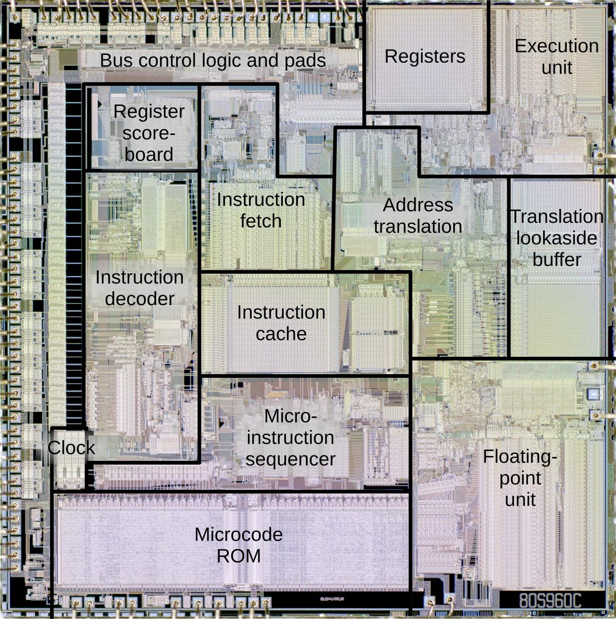
The strangest thing about these four architectures is that the chips were identical, using the same die. In other words, the simple Core chip included all the circuitry for floating point, memory management, and objects; these features just weren't used.12 The die photo below shows the die, with the main functional units labeled. Around the edge of the die are the bond pads that connect the die to the external pins. Note that the right half of the chip has almost no bond pads. As a result, the packaged IC had many unused pins.13

The i960 KA/KB/MC/XA with the main functional blocks labeled. Click this image (or any other) for a larger version. Die image courtesy of Antoine Bercovici.  Floorplan from The 80960 microprocessor architecture.

The i960 KA/KB/MC/XA with the main functional blocks labeled. Click this image (or any other) for a larger version. Die image courtesy of Antoine Bercovici. Floorplan from The 80960 microprocessor architecture.

One advanced feature of the i960 is register scoreboarding, visible in the upper-left corner of the die. The idea is that loading a register from memory is slow, so to improve performance, the processor executes the following instructions while the load completes, rather than waiting. Of course, an instruction can't be executed if it uses a register that is being loaded, since the value isn't there. The solution is a "scoreboard" that tracks which registers are valid and which are still being loaded, and blocks an instruction if the register isn't ready. The i960 could handle up to three outstanding reads, providing a significant performance gain.

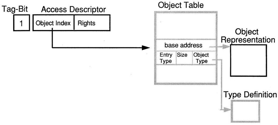
The most complex i960 architecture is the Extended architecture, which provides the object-oriented system. This architecture is designed around an unforgeable pointer called an Access Descriptor that provides protected access to an object. What makes the pointer unforgeable is that it is 33 bits long with an extra bit that indicates an Access Descriptor. You can't set this bit with a regular 32-bit instruction. Instead, an Access Descriptor can only be created with a special privileged instruction, "Create AD".14

An Access Descriptor is a pointer to an object table. From BiiN Object Computing.

An Access Descriptor is a pointer to an object table. From BiiN Object Computing.

The diagram above shows how objects work. The 33-bit Access Descriptor (AD) has its tag bit set to 1, indicating that it is a valid Access Descriptor. The Rights field controls what actions can be performed by this object reference. The AD's Object Index references the Object Table that holds information about each object. In particular, the Base Address and Size define the object's location in memory and ensure that an access cannot exceed the bounds of the object. The Type Definition defines the various operations that can be performed on the object. Since this is all implemented by the processor at the instruction level, it provides strict security.

Gemini and BiiN

The i960 was heavily influenced by a partnership called Gemini and then BiiN. In 1983, near the start of the i960 project, Intel formed a partnership with Siemens to build high-performance fault-tolerant servers. In this partnership, Intel would provide the hardware while Siemens developed the software. This partnership allowed Intel to move beyond the chip market to the potentially-lucrative systems market, while adding powerful systems to Siemens' product line. The Gemini team contained many of the people from the 432 project and wanted to continue the 432's architecture. Gemini worked closely with the developers of the i960 to ensure the new processor would meet their needs; both teams worked in the same building at Intel's Jones Farm site in Oregon.

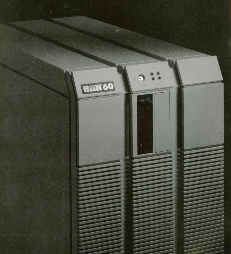
The BiiN 60 system. From BiiN 60 Technical Overview.

The BiiN 60 system. From BiiN 60 Technical Overview.

In 1988, shortly after the announcement of the i960 chips, the Intel/Siemens partnership was spun off into a company called BiiN.15 BiiN announced two high-performance, fault-tolerant, multiprocessor systems. These systems used the i960 XA processor16 and took full advantage of the object-oriented model and other features provided by its Extended architecture. The BiiN 20 was designed for departmental computing and cost $43,000 to $80,000. It supported 50 users (connected by terminals) on one 5.5-MIPS i960 processor. The larger BiiN 60 handled up to 1000 terminals and cost $345,000 to $815,000. The Unix-compatible BiiN operating system (BiiN/OS) and utilities were written in 2 million lines of Ada code.

BiiN described many potential markets for these systems: government, factory automation, financial services, on-line transaction processing, manufacturing, and health care. Unfortunately, as ExtremeTech put it, "the market for fault-tolerant Unix workstations was approximately nil." BiiN was shut down in 1989, just 15 months after its creation as profitability kept becoming more distant. BiiN earned the nickname "Billions invested in Nothing"; the actual investment was 1700 person-years and $430 million.

The superscalar i960 CA

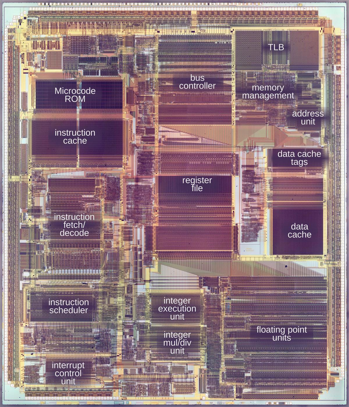
One year after the first i960, Intel released the groundbreaking i960 CA. This chip was the world's first superscalar microprocessor, able to execute more than one instruction per clock cycle. The chip had three execution units that could operate in parallel: an integer execution unit, a multiply/divide unit, and an address generation unit that could also do integer arithmetic.17 To keep the execution units busy, the i960 CA's instruction sequencer examined four instructions at once and determined which ones could be issued in parallel without conflict. It could issue two instructions and a branch each clock cycle, using branch prediction to speculatively execute branches out of order.

The i960 CA die, with functional blocks labeled. Photo courtesy of Antoine Bercovici. Functional blocks from the datasheet.

The i960 CA die, with functional blocks labeled. Photo courtesy of Antoine Bercovici. Functional blocks from the datasheet.

Following the CA, several other superscalar variants were produced: the CF had more cache, the military MM implemented the Protected architecture (memory management and a floating point unit), and the military MX implemented the Extended architecture (object-oriented).

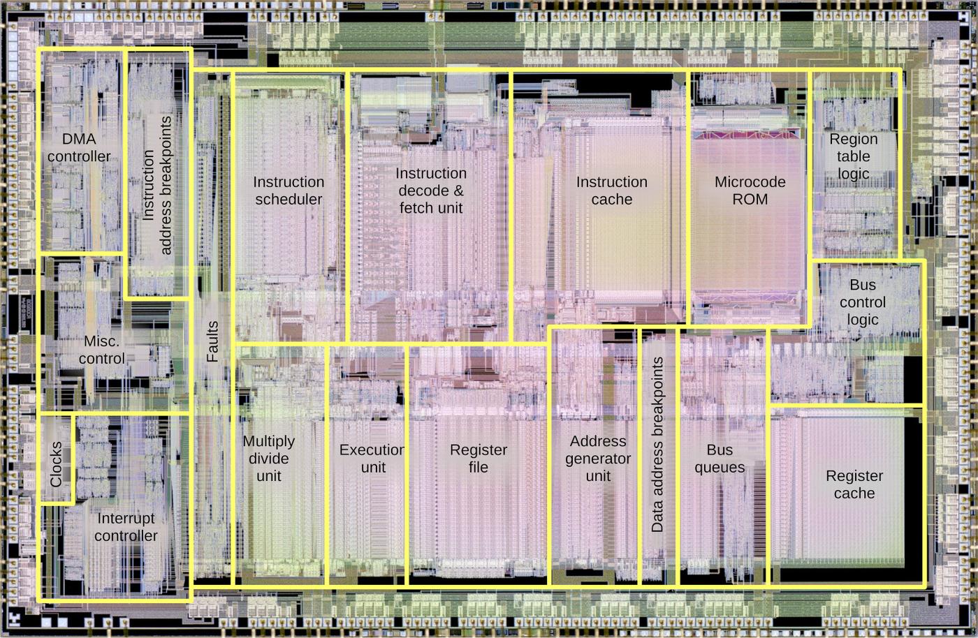
The image below shows the 960 MX die with the main functional blocks labeled. (I think the MM and MX used the same die but I'm not sure.18) Like the i960 CA, this chip has multiple functional units that can be operated in parallel for its superscalar execution. Note the wide buses between various blocks, allowing high internal bandwidth. The die was too large for the optical projection of the mask, with the result that the corners of the circuitry needed to be rounded off.

The i960MX die with the main functional blocks labeled. This is a die photo I took, with labels based on my reverse engineering.

The i960MX die with the main functional blocks labeled. This is a die photo I took, with labels based on my reverse engineering.

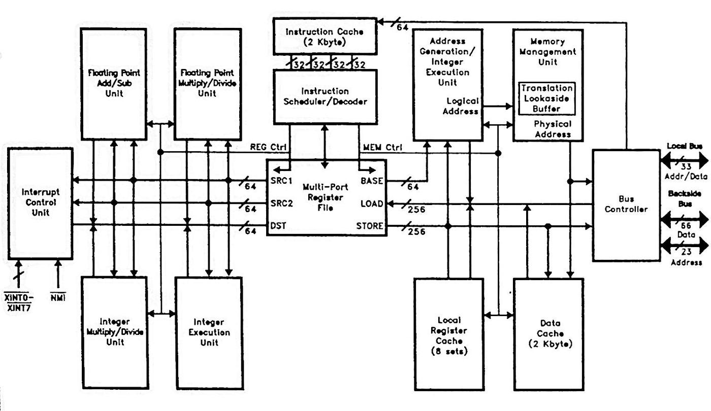
The block diagram of the i960 MX shows the complexity of the chip and how it is designed for parallelism. The register file is the heart of the chip. It is multi-ported so up to 6 registers can be accessed at the same time. Note the multiple, 256-bit wide buses between the register file and the various functional units. The chip has two buses: a high-bandwidth Backside Bus between the chip and its external cache and private memory; and a New Local Bus, which runs at half the speed and connects the chip to main memory and I/O. For highest performance, the chip's software would access its private memory over the high-speed bus, while using the slower bus for I/O and shared memory accesses.

A functional block diagram of the i960 MX. From Intel Military and Special Projects Handbook, 1993.

A functional block diagram of the i960 MX. From Intel Military and Special Projects Handbook, 1993.

Military use and the JIAWG standard

The i960 had a special role in the US military. In 1987 the military mandated the use of Ada as the single, common computer programming language for Defense computer resources in most cases.19 In 1989, the military created the JIAWG standard, which selected two 32-bit instruction set architectures for military avionics. These architectures were the i960's Extended architecture (implemented by the i960 XA) and the MIPS architecture (based on a RISC project at Stanford).20 The superscalar i960 MX processor described earlier soon became a popular JIAWG-compliant processor, since it had higher performance than the XA.

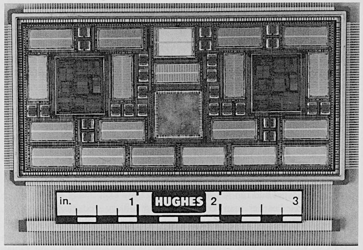
Hughes designed a modular avionics processor that used the i960 XA and later the MX. A dense module called the HAC-32 contained two i960 MX processors, 2 MB of RAM, and an I/O controller in a 2"×4" multi-chip module, slightly bigger than a credit card. This module had bare dies bonded to the substrate, maximizing the density. In the photo below, the two largest dies are the i960 MX while the numerous gray rectangles are memory chips. This module was used in F-22's Common Integrated Processor, the RAH-66 Comanche helicopter (which was canceled), the F/A-18's Stores Management Processor (the computer that controls attached weapons), and the AN/ALR-67 radar computer.

The Hughes HAC-32. From Avionics Systems Design.

The Hughes HAC-32. From Avionics Systems Design.

The military market is difficult due to the long timelines of military projects, unpredictable volumes, and the risk of cancellations. In the case of the F-22 fighter plane, the project started in 1985 when the Air Force sent out proposals for a new Advanced Tactical Fighter. Lockheed built a YF-22 prototype, first flying it in 1990. The Air Force selected the YF-22 over the competing YF-23 in 1991 and the project moved to full-scale development. During this time, at least three generations of processors became obsolete. In particular, the i960MX was out of production by the time the F-22 first flew in 1997. At one point, the military had to pay Intel $22 million to restart the i960 production line. In 2001, the Air Force started a switch to the PowerPC processor, and finally the plane entered military service in 2005. The F-22 illustrates how the fast-paced obsolescence of processors is a big problem for decades-long military projects.

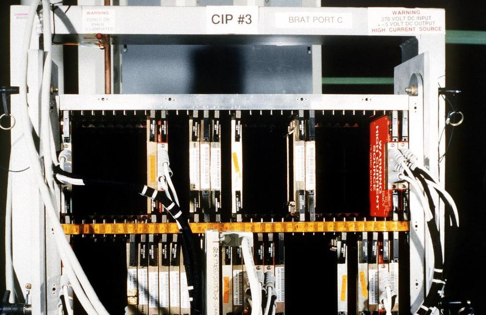
The Common Integrated Processor for the F-22, presumably with i960 MX chips inside. It is the equivalent of two Cray supercomputers and was the world's most advanced, high-speed computer system for a fighter aircraft. Source: NARA/Hughes Aircraft Co./T.W. Goosman.

The Common Integrated Processor for the F-22, presumably with i960 MX chips inside. It is the equivalent of two Cray supercomputers and was the world's most advanced, high-speed computer system for a fighter aircraft. Source: NARA/Hughes Aircraft Co./T.W. Goosman.

Intel charged thousands of dollars for each i960 MX and each F-22 contained a cluster of 35 i960 MX processors, so the military market was potentially lucrative. The Air Force originally planned to buy 750 planes, but cut this down to just 187, which must have been a blow to Intel. As for the Comanche helicopter, the Army planned to buy 1200 of them, but the program was canceled entirely after building two prototypes. The point is that the military market is risky and low volume even in the best circumstances.21 In 1998, Intel decided to leave the military business entirely, joining AMD and Motorola.

Foreign militaries also made use of the i960. In 2008 a businessman was sentenced to 35 months in prison for illegally exporting hundreds of i960 chips into India for use in the radar for the Tejas Light Combat Aircraft.

i960: the later years

By 1990, the i960 was selling well, but the landscape at Intel had changed. The 386 processor was enormously successful, due to the Compaq Deskpro 386 and other systems, leading to Intel's first billion-dollar quarter. The 8086 had started as a stopgap processor to fill a temporary marketing need, but now the x86 was Intel's moneymaking engine. As part of a reorganization, the i960 project was transferred to Chandler, Arizona. Much of the i960 team in Oregon moved to the newly-formed Pentium Pro team, while others ended up on the 486 DX2 processor. This wasn't the end of the i960, but the intensity had reduced.

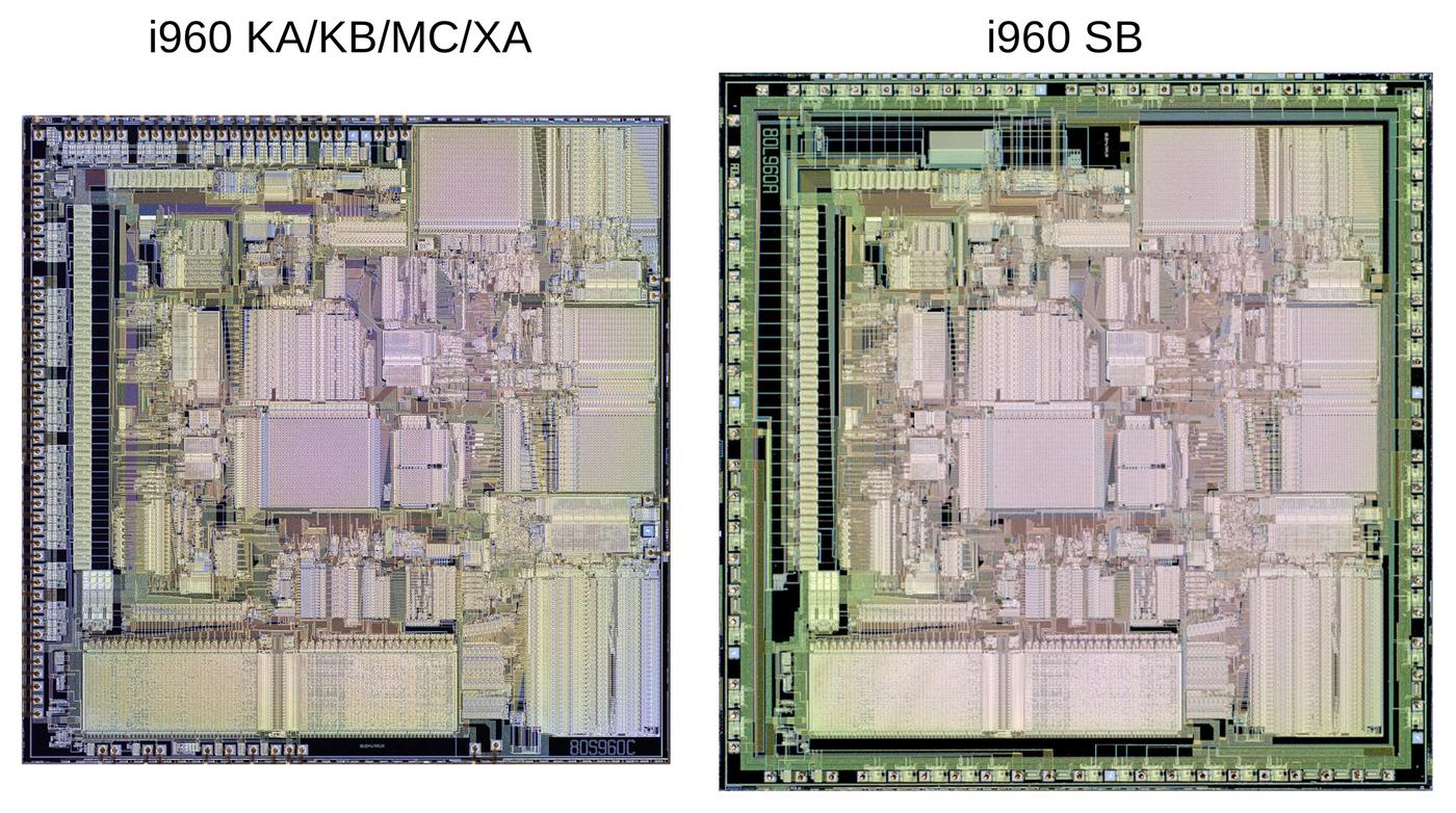
To reduce system cost, Intel produced versions of the i960 that had a 16-bit bus, although the processor was 32 bits internally. (This is the same approach that Intel used with the 8088 processor, a version of the 8086 processor with an 8-bit bus instead of 16.) The i960 SB had the "Numerics" architecture, that is, with a floating-point unit. Looking at the die below, we can see that the SB design is rather "lazy", simply the previous die (KA/KB/MC/XA) with a thin layer of circuitry around the border to implement the 16-bit bus. Even though the SB didn't support memory management or objects, Intel didn't remove that circuitry. The process was reportedly moved from 1.5 microns to 1 micron, shrinking the die to 270 mils square.

Comparison of the original i960 die and the i960 SB. Photos courtesy of Antoine Bercovici.

Comparison of the original i960 die and the i960 SB. Photos courtesy of Antoine Bercovici.

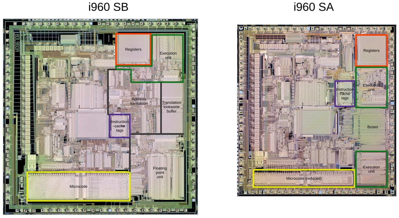
The next chip, the i960 SA, was the 16-bit-bus "Core" architecture, without floating point. The SA was based on the SB but Intel finally removed unused functionality from the die, making the die about 24% smaller. The diagram below shows how the address translation, translation lookaside buffer, and floating point unit were removed, along with much of the microcode (yellow). The instruction cache tags (purple), registers (orange), and execution unit (green) were moved to fit into the available space. The left half of the chip remained unchanged. The driver circuitry around the edges of the chip was also tightened up, saving a bit of space.

This diagram compares the SB and SA chips. Photos courtesy of Antoine Bercovici.

This diagram compares the SB and SA chips. Photos courtesy of Antoine Bercovici.

Intel introduced the high-performance Hx family around 1994. This family was superscalar like the CA/CF, but the Hx chips also had a faster clock, had much more cache, and included additional functionality such as timers and a guarded memory unit. The Jx family was introduced as the midrange, cost-effective line, faster and better than the original chips but not superscalar like the Hx. Intel attempted to move the i960 into the I/O controller market with the Rx family and the VH.23 This was part of Intel's Intelligent Input/Output specification (I2O), which was a failure overall.

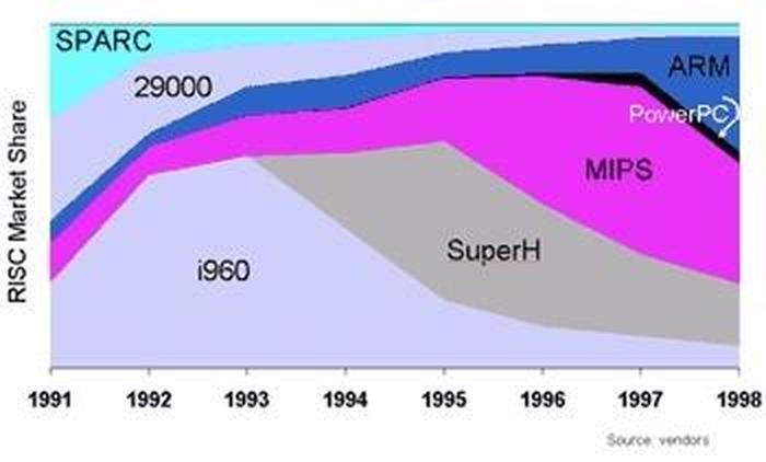
For a while, the i960 was a big success in the marketplace and was used in many products. Laser printers and graphical terminals were key applications, both taking advantage of the i960's high speed to move pixels. The i960 was the world's best-selling RISC chip in 1994. However, without focused development, the performance of the i960 fell behind the competition, and its market share rapidly dropped.

Market share of embedded RISC processors. From ExtremeTech.

Market share of embedded RISC processors. From ExtremeTech.

By the late 1990s, the i960 was described with terms such as "aging", "venerable", and "medieval". In 1999, Microprocessor Report described the situation: "The i960 survived on cast-off semiconductor processes two to three generations old; the i960CA is still built in a 1.0-micron process (perhaps by little old ladies with X-Acto knives)."22

One of the strongest competitors was DEC's powerful StrongARM processor design, a descendant of the ARM chip. Even Intel's top-of-the-line i960HT fared pitifully against the StrongARM, with worse cost, performance, and power consumption. In 1997, DEC sued Intel, claiming that the Pentium infringed ten of DEC's patents. As part of the complex but mutually-beneficial 1997 settlement, Intel obtained rights to the StrongARM chip. As Intel turned its embedded focus from i960 to StrongARM, one writer wrote, "Things are looking somewhat bleak for Intel Corp's ten-year-old i960 processor." The i960 limped on for another decade until Intel officially ended production in 2007.

RISC or CISC?

The i960 challenges the definitions of RISC and CISC processors.24 It is generally considered a RISC processor, but its architect says "RISC techniques were used for high performance, CISC techniques for ease of use."25 John Mashey of MIPS described it as on the RISC/CISC border26 while Steve Furber (co-creator of ARM) wrote that it "includes many RISC ideas, but it is not a simple chip" with "many complex instructions which make recourse to microcode" and a design that "is more reminiscent of a complex, mainframe architecture than a simple, pipelined RISC." And they were talking about the i960 KB with the simple Numerics architecture, not the complicated Extended architecture!

Even the basic Core architecture has many non-RISC-like features. It has microcoded instructions that take multiple cycles (such as integer multiplication), numerous addressing modes27, and unnecessary instructions (e.g. AND NOT as well as NOT AND). It also has a large variety of datatypes, even more than the 432: integer (8, 16, 32, or 64 bit), ordinal (8, 16, 32, or 64 bit), decimal digits, bit fields, triple-word (96 bits), and quad-word (128 bits). The Numerics architecture adds floating-point reals (32, 64, or 80 bit) while the Protected architecture adds byte strings with decidedly CISC-like instructions to act on them.28

When you get to the Extended architecture with objects, process management, and interprocess communication instructions, the large instruction set seems obviously CISC.29 (The instruction set is essentially the same as 432 and the 432 is an extremely CISC processor.) You could argue that the i960 Core architecture is RISC and the Extended architecture is CISC, but the problem is that they are identical chips.

Of course, it doesn't really matter if the i960 is considered RISC, CISC, or CISC instructions running on a RISC core. But the i960 shows that RISC and CISC aren't as straightforward as they might seem.

Summary

The i960 chips can be confusing since there are four architectures, along with scalar vs. superscalar, and multiple families over time. I've made the table below to summarize the i960 family and the approximate dates. The upper entries are the scalar families while the lower entries are superscalar. The columns indicate the four architectural variants; although the i960 started with four variants, eventually Intel focused on only the Core. Note that each "x" family represents multiple chips.

CoreNumericsProtectedExtended
KAKBMCXAOriginal (1988)
SASB  Entry level, 16-bit data bus (1991)
Jx   Midrange (1993-1998)
Rx,VH   I/O interface (1995-2001)
CA,CF MMMXSuperscalar (1989-1992)
Hx   Superscalar, higher performance (1994)

Although the i960 is now mostly forgotten, it was an innovative processor for the time. The first generation was Intel's first RISC chip, but pushed the boundary of RISC with many CISC-like features. The i960 XA literally set the standard for military computing, selected by the JIAWG as the military's architecture. The i960 CA provided a performance breakthrough with its superscalar architecture. But Moore's Law means that competitors can rapidly overtake a chip, and the i960 ended up as history.

Thanks to Glen Myers, Kevin Kahn, Steven McGeady, and others from Intel for answering my questions about the i960. Thanks to Prof. Paul Lubeck for obtaining documentation for me. I plan to write more, so follow me on Twitter @kenshirriff or RSS for updates. I've also started experimenting with Mastodon recently as @[email protected] and Bluesky as @righto.com so you can follow me there too.

Notes and references

  1. The 432 used two chips for the processor and a third chip for I/O. At the time, these were said to be "three of the largest integrated circuits in history." The first processor chip contained more than 100,000 devices, making it "one of the densest VLSI circuits to have been fabricated so far." The article also says that the 432 project "was the largest investment in a single program that Intel has ever made." See Ada determines architecture of 32-bit microprocessor, Electronics, Feb 24, 1981, pages 119-126, a very detailed article on the 432 written by the lead engineer and the team's manager. 

  2. The performance problems of the iAPX 432 were revealed by a student project at Berkeley, A performance evaluation of the Intel iAPX 432, which compared its performance with the VAX-11/780, Motorola 68000, and Intel 8086. Instead of providing mainframe performance, the 432 had a fraction of the performance of the competing systems. Another interesting paper is Performance effects of architectural complexity in the Intel 432, which examines in detail what the 432 did wrong. It concludes that the 432 could have been significantly faster, but would still have been slower than its contemporaries. An author of the paper was Robert Colwell, who was later hired by Intel and designed the highly-successful Pentium Pro architecture. 

  3. You might expect the 8086, 186, and 286 processors to form a nice progression, but it's a bit more complicated. The 186 and 286 processors were released at the same time. The 186 essentially took the 8086 and several support chips and integrated them onto a single die. The 286, on the other hand, extended the 8086 with memory management. However, its segment-based memory management was a bad design, using ideas from the Zilog MMU, and wasn't popular. The 286 also had a protected mode, so multiple processes could be isolated from each other. Unfortunately, protected mode had some serious problems. Bill Gates famously called the 286 "brain-damaged" echoing PC Magazine editor Bill Machrone and writer Jerry Pournelle, who both wanted credit for originating the phrase.

    By 1984, however, the 286 was Intel's star due to growing sales of IBM PCs and compatibles that used the chip. Intel's 1984 annual report featured "The Story of the 286", a glowing 14-page tribute to the 286. 

  4. Given IBM's success with IBM PC, Intel was puzzled that IBM wasn't interested in the 386 processor. It turned out that IBM had a plan to regain control of the PC so they could block out competitors that were manufacturing IBM PC compatibles. IBM planned to reverse-engineer Intel's 286 processor and build its own version. The computers would run the OS/2 operating system instead of Windows and use the proprietary Micro Channel architecture. However, the reverse-engineering project failed and IBM eventually moved to the Intel 386 processor. The IBM PS/2 line of computers, released in 1987, followed the rest of the plan. However, the PS/2 line was largely unsuccessful; rather than regaining control over the PC, IBM ended up losing control to companies such as Compaq and Dell. (For more, see Creating the Digital Future, page 131.) 

  5. The 386 team created an oral history that describes the development of the 386 in detail. Pages 5, 6, and 19 are most relevant to this post. 

  6. You might wonder why the processor was codenamed P4, since logically P4 should indicate the 486. Confusingly, Intel's processor codenames were not always sequential and they sometimes reused numbers. The numbers apparently started with P0, the codename for the Optimal Terminal Kit, a processor that didn't get beyond early planning. P5 was used for the 432, P4 for the planned follow-on, P7 for the i960, P10 for the i960 CA, and P12 for the i960 MX. (Apparently they thought that x86 wouldn't ever get to P4.)

    For the x86 processors, P1 through P6 indicated the 186, 286, 386, 486, 586, Pentium, and Pentium Pro as you'd expect. (The Pentium used a variety of codes for various versions, such as P54C, P24T, and P55C; I don't understand the pattern behind these.) For some reason, the i386SX was the P9 and the i486SX was the P23 and the i486DX2 was the P24. The Pentium 4 Willamette was the first new microarchitecture (NetBurst) since P6 so it was going to be P7, but Itanium took the P7 name codename so Willamette became P68. After that, processors were named after geographic features, avoiding the issues with numeric codenames.

    Other types of chips used different letter prefixes. The 387 numeric coprocessor was the N3. The i860 RISC processor was originally the N10, a numeric co-processor. The follow-on i860 XP was the N11. Support chips for the 486 included the C4 cache chip and the unreleased I4 interrupt controller. 

  7. At the time, Intel had a family of 16-bit embedded microcontrollers called MCS-96 featuring the 8096. The 80960 name was presumably chosen to imply continuity with the 8096 16-bit microcontrollers (MCS-96), even though the 8096 and the 80960 are completely different. (I haven't been able to confirm this, though.) Intel started calling the chip the "i960" around 1989. (Intel's chip branding is inconsistent: from 1987 to 1991, Intel's annual reports called the 386 processor the 80386, the 386, the Intel386, and the i386. I suspect their trademark lawyers were dealing with the problem that numbers couldn't be trademarked, which was the motivation for the "Pentium" name rather than 586.)

    Note that the i860 processor is completely unrelated to the i960 despite the similar numbers. They are both 32-bit RISC processors, but are architecturally unrelated. The i860 was targeted at high-performance workstations, while the i960 was targeted at embedded applications. For details on the i860, see The first million-transistor chip

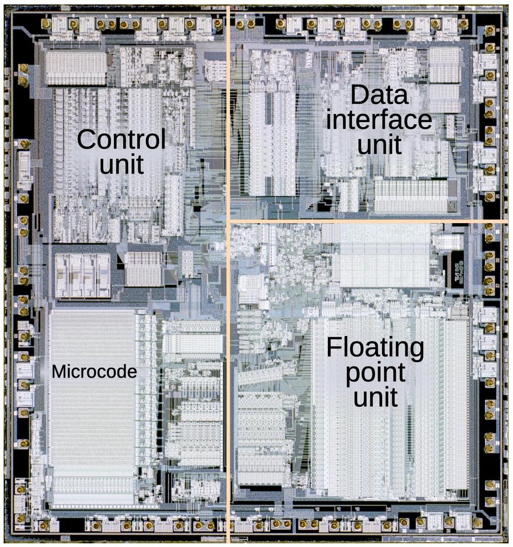
  8. The Intel 80387 floating-point coprocessor chip used the same floating-point unit as the i960. The diagram below shows the 80387; compare the floating-point unit in the lower right corner with the matching floating-point unit in the i960 KA or SB die photo.

    The 80837 floating-point coprocessor with the main functional blocks labeled. Die photo courtesy of Antoine Bercovici. 80387 floor plan from The 80387 and its applications.

    The 80837 floating-point coprocessor with the main functional blocks labeled. Die photo courtesy of Antoine Bercovici. 80387 floor plan from The 80387 and its applications.


  9. I compared the instruction sets of the 432 and i960 and the i960 Extended instruction set seems about as close as you could get to the 432 while drastically changing the underlying architecture. If you dig into the details of the object models, there are some differences. Some instructions also have different names but the same function. 

  10. The first i960 chips were described in detail in the 1988 book The 80960 microprocessor architecture by Glenford Myers (who was responsible for the 80960 architecture at Intel) and David Budde (who managed the VLSI development of the 80960 components). This book discussed three levels of architecture (Core, Numerics, and Protected). The book referred to the fourth level, the Extended architecture (XA), calling it "a proprietary higher level of the architecture developed for use by Intel in system products" and did not discuss it further. These "system products" were the systems being developed at BiiN. 

  11. I could find very little documentation on the Extended architecture. The 80960XA datasheet provides a summary of the instruction set. The i960 MX datasheet provides a similar summary; it is in the Intel Military and Special Products databook, which I found after much difficulty. The best description I could find is in the 400-page BiiN CPU architecture reference manual. Intel has other documents that I haven't been able to find anywhere: i960 MM/MX Processor Hardware Reference Manual, and Military i960 MM/MX Superscalar Processor. (If you have one lying around, let me know.)

    The 80960MX Specification Update mentions a few things about the MX processor. My favorite is that if you take the arctan of a value greater than 32768, the processor may lock up and require a hardware reset. Oops. The update also says that the product is sold in die and wafer form only, i.e. without packaging. Curiously, earlier documentation said the chip was packaged in a 348-pin ceramic PGA package (with 213 signal pins and 122 power/ground pins). I guess Intel ended up only supporting the bare die, as in the Hughes HAC-32 module. 

  12. According to people who worked on the project, there were not even any bond wire changes or blown fuses to distinguish the chips for the four different architectures. It's possible that Intel used binning, selling dies as a lower architecture if, for example, the floating point unit failed testing. Moreover, the military chips presumably had much more extensive testing, checking the military temperature range for instance. 

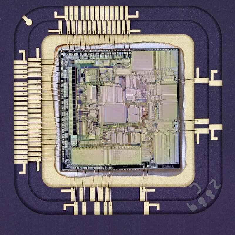
  13. The original i960 chips (KA/KB/MC/XA) have a large number of pins that are not connected (marked NC on the datasheet). This has led to suspicious theorizing, even on Wikipedia, that these pins were left unconnected to control access to various features. This is false for two reasons. First, checking the datasheets shows that all four chips have the same pinout; there are no pins connected only in the more advanced versions. Second, looking at the packaged chip (below) explains why so many pins are unconnected: much of the chip has no bond pads, so there is nothing to connect the pins to. In particular, the right half of the die has only four bond pads for power. This is an unusual chip layout, but presumably the chip's internal buses made it easier to put all the connections at the left. The downside is that the package is more expensive due to the wasted pins, but I expect that BiiN wasn't concerned about a few extra dollars for the package.

    The i960 MC die, bonded in its package. Photo courtesy of Antoine Bercovici.

    The i960 MC die, bonded in its package. Photo courtesy of Antoine Bercovici.

    But you might wonder: the simple KA uses 32 bits and the complex XA uses 33 bits, so surely there must be another pin for the 33rd bit. It turns out that pin F3 is called CACHE on the KA and CACHE/TAG on the XA. The pin indicates if an access is cacheable, but the XA uses the pin during a different clock cycle to indicate whether the 32-bit word is data or an access descriptor (unforgeable pointer).

    So how does the processor know if it should use the 33-bit object mode or plain 32-bit mode? There's a processor control word called Processor Controls, that includes a Tag Enable bit. If this bit is set, the processor uses the 33rd bit (the tag bit) to distinguish Access Descriptors from data. If the bit is clear, the distinction is disabled and the processor runs in 32-bit mode. (See BiiN CPU Architecture Reference Manual section 16.1 for details.) 

  14. The 432 and the i960 both had unforgeable object references, the Access Descriptor. However, the two processors implemented Access Descriptors in completely different ways, which is kind of interesting. The i960 used a 33rd bit as a Tag bit to distinguish an Access Descriptor from a regular data value. Since the user didn't have access to the Tag bit, the user couldn't create or modify Access Descriptors. The 432, on the other hand, used standard 32-bit words. To protect Access Descriptors, each object was divided into two parts, each protected by a length field. One part held regular data, while the other part held Access Descriptors. The 432 had separate instructions to access the two parts of the object, ensuring that regular instructions could not tamper with Access Descriptors. 

  15. The name "BiiN" was developed by Lippincott & Margulies, a top design firm. The name was designed for a strong logo, as well as referencing binary code (so it was pronounced as "bine"). Despite this pedigree, "BiiN" was called one of the worst-sounding names in the computer industry, see Losing the Name Game

  16. Some sources say that BiiN used the i960 MX, not the XA, but they are confused. A paper from BiiN states that BiiN used the 80960 XA. (Sadly, BiiN was so short-lived that the papers introducing the BiiN system also include its demise.) Moreover, BiiN shut down in 1989 while the i960 MX was introduced in 1990, so the timeline doesn't work. 

  17. The superscalar i960 architecture is described in detail in The i960CA SuperScalar implementation of the 80960 architecture and Inside Intel's i960CA superscalar processor while the military MM version is described in Performance enhancements in the superscalar i960MM embedded microprocessor

  18. I don't have a die photo of the i960 MM, so I'm not certain of the relationship between the MM and the MX. The published MM die size is approximately the same as the MX. The MM block diagram matches the MX, except using 32 bits instead of 33. Thus, I think the MM uses the MX die, ignoring the Extended features, but I can't confirm this. 

  19. The military's Ada mandate remained in place for a decade until it was eliminated in 1997. Ada continues to be used by the military and other applications that require high reliability, but by now C++ has mostly replaced it. 

  20. The military standard was decided by the Joint Integrated Avionics Working Group, known as JIAWG. Earlier, in 1980, the military formed a 16-bit computing standard, MIL-STD-1750A. The 1750A standard created a new architecture, and numerous companies implemented 1750A-compatible processors. Many systems used 1750A processors and overall it was more successful than the JIAWG standard. 

  21. Chip designer and curmudgeon Nick Tredennick described the market for Intel's 960MX processor: "Intel invested considerable money and effort in the design of the 80960MX processor, for which, at the time of implementation, the only known application was the YF-22 aircraft. When the only prototype of the YF-22 crashed, the application volume for the 906MX actually went to zero; but even if the program had been successful, Intel could not have expected to sell more than a few thousand processors for that application." 

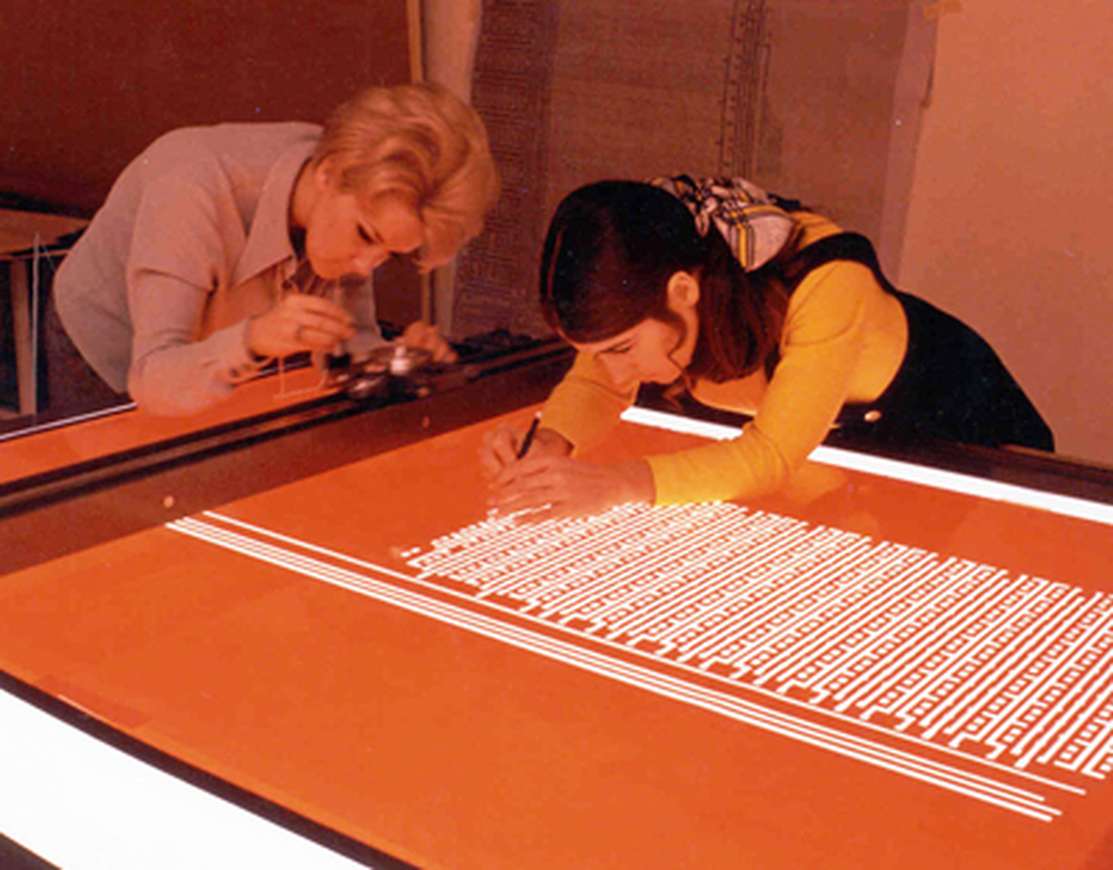
  22. In the early 1970s, chip designs were created by cutting large sheets of Rubylith film with X-Acto knives. Of course, that technology was long gone by the time of the i960.

    Intel photo of two women cutting Rubylith.

    Intel photo of two women cutting Rubylith.


  23. The Rx I/O processor chips combined a Jx processor core with a PCI bus interface and other hardware. The RM and RN versions were introduced in 2000 with a hardware XOR engine for RAID disk array parity calculations. The i960 VH (1998) was similar to Rx, but had only one PCI bus, no APIC bus, and was based on the JT core. The 80303 (2000) was the end of the i960 I/O processors. The 80303 was given a numeric name instead of an i960 name because Intel was transitioning from i960 to XScale at the time. The numeric name makes it look like a smooth transition from the 80303 (i960) I/O processor to the XScale-based I/O processors such as the 80333. The 803xx chips were also called IOP3xx (I/O Processor); some were chipsets with a separate XScale processor chip and an I/O companion chip.  

  24. Although the technical side of RISC vs. CISC is interesting, what I find most intriguing is the "social history" of RISC: how did a computer architecture issue from the 1980s become a topic that people still vigorously argue over 40 years later? I see several factors that keep the topic interesting:

    • RISC vs. CISC has a large impact on not only computer architects but also developers and users.
    • The topic is simple enough that everyone can have an opinion. It's also vague enough that nobody agrees on definitions, so there's lots to argue about.
    • There are winners and losers, but no resolution. RISC sort of won in the sense that almost all new instruction set architectures have been RISC. But CISC has won commercially with the victory of x86 over SPARC, PowerPC, Alpha, and other RISC contenders. But ARM dominates mobile and is moving into personal computers through Apple's new processors. If RISC had taken over in the 1980s as expected, there wouldn't be anything to debate. But x86 has prospered despite the efforts of everyone (including Intel) to move beyond it.
    • RISC vs. CISC takes on a "personal identity" aspect. For instance, if you're an "Apple" person, you're probably going to be cheering for ARM and RISC. But nobody cares about branch prediction strategies or caching.

    My personal opinion is that it is a mistake to consider RISC and CISC as objective, binary categories. (Arguing over whether ARM or the 6502 is really RISC or CISC is like arguing over whether a hotdog is a sandwich RISC is more of a social construct, a design philosophy/ideology that leads to a general kind of instruction set architecture that leads to various implementation techniques.

    Moreover, I view RISC vs. CISC as mostly irrelevant since the 1990s due to convergence between RISC and CISC architectures. In particular, the Pentium Pro (1995) decoded CISC instructions into "RISC-like" micro-operations that are executed by a superscalar core, surprising people by achieving RISC-like performance from a CISC processor. This has been viewed as a victory for CISC, a victory for RISC, nothing to do with RISC, or an indication that RISC and CISC have converged. 

  25. The quote is from Microprocessor Report April 1988, "Intel unveils radical new CPU family", reprinted in "Understanding RISC Microprocessors". 

  26. John Mashey of MIPS wrote an interesting article "CISCs are Not RISCs, and Not Converging Either" in the March 1992 issue of Microprocessor Report, extending a Usenet thread. It looks at multiple quantitative factors of various processors and finds a sharp line between CISC processors and most RISC processors. The i960, Intergraph Clipper, and (probably) ARM, however, were "truly on the RISC/CISC border, and, in fact, are often described that way." 

  27. The i960 datasheet lists an extensive set of addressing modes, more than typical for a RISC chip:

    • 12-bit offset
    • 32-bit offset
    • Register-indirect
    • Register + 12-bit offset
    • Register + 32-bit offset
    • Register + index-register×scale-factor
    • Register×scale-factor + 32-bit displacement
    • Register + index-register×scale-factor + 32-bit displacement
    where the scale-factor is 1, 2, 4, 8, or 16.

    See the 80960KA embedded 32-bit microprocessor datasheet for more information. 

  28. The i960 MC has string instructions that move, scan, or fill a string of bytes with a specified length. These are similar to the x86 string operations, but these are very unusual for a RISC processor. 

  29. The iAPX 432 instruction set is described in detail in chapter 10 of the iAPX 432 General Data Processor Architecture Reference Manual; the instructions are called "operators". The i960 Protected instruction set is listed in the 80960MC Programmer's Reference Manual while the i960 Extended instruction set is described in the BiiN CPU architecture reference manual.

    The table below shows the instruction set for the Extended architecture, the full set of object-oriented instructions. The instruction set includes typical RISC instructions (data movement, arithmetic, logical, comparison, etc), floating point instructions (for the Numerics architecture), process management instructions (for the Protected architecture), and the Extended object instructions (Access Descriptor operations). The "Mixed" instructions handle 33-bit values that can be either a tag (object pointer) or regular data. Note that many of these instructions have separate opcodes for different datatypes, so the complete instruction set is larger than this list, with about 240 opcodes.

    The Extended instruction set, from the i960 XA datasheet. Click for a larger version.
    The Extended instruction set, from the i960 XA datasheet. Click for a larger version.
Tracing the roots of the 8086 instruction set to the Datapoint 2200 minicomputer

The Intel 8086 processor started the x86 architecture that is still extensively used today. The 8086 has some quirky characteristics: it is little-endian, has a parity flag, and uses explicit I/O instructions instead of just memory-mapped I/O. It has four 16-bit registers that can be split into 8-bit registers, but only one that can be used for memory indexing. Surprisingly, the reason for these characteristics and more is compatibility with a computer dating back before the creation of the microprocessor: the Datapoint 2200, a minicomputer with a processor built out of TTL chips. In this blog post, I'll look in detail at how the Datapoint 2200 led to the architecture of Intel's modern processors, step by step through the 8008, 8080, and 8086 processors.

The Datapoint 2200

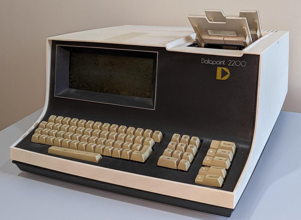
In the late 1960s, 80-column IBM punch cards were the primary way of entering data into computers, although CRT terminals were growing in popularity. The Datapoint 2200 was designed as a low-cost terminal that could replace a keypunch, with a squat CRT display the size of a punch card. By putting some processing power into the Datapoint 2200, it could perform data validation and other tasks, making data entry more efficient. Even though the Datapoint 2200 was typically used as an intelligent terminal, it was really a desktop minicomputer with a "unique combination of powerful computer, display, and dual cassette drives." Although now mostly forgotten, the Datapoint 2200 was the origin of the 8-bit microprocessor, as I'll explain below.

The Datapoint 2200 computer (Version II).

The Datapoint 2200 computer (Version II).

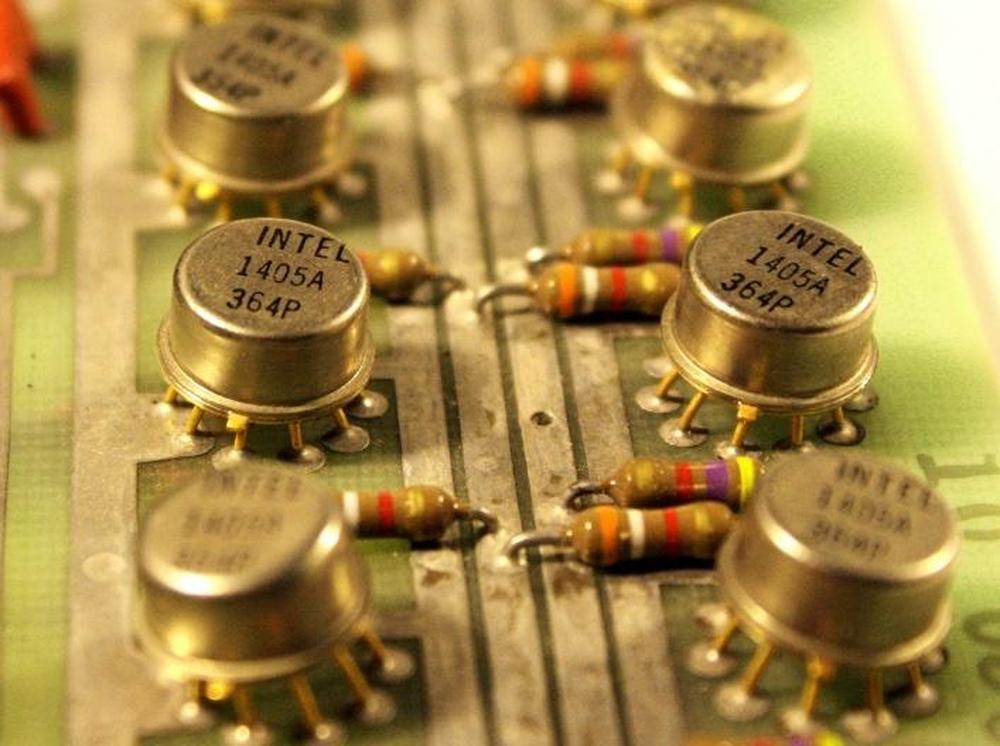
The memory storage of the Datapoint 2200 had a large impact on its architecture and thus the architecture of today's computers. In the 1960s and early 1970s, magnetic core memory was the dominant form of computer storage. It consisted of tiny ferrite rings, threaded into grids, with each ring storing one bit. Magnetic core storage was bulky and relatively expensive, though. Semiconductor RAM was new and very expensive; Intel's first product in 1969 was a RAM chip called the 3101, which held just 64 bits and cost $99.50. To minimize storage costs, the Datapoint 2200 used an alternative: MOS shift-register memory. The Intel 1405 shift-register memory chip provided much more storage than RAM chips at a much lower cost (512 bits for $13.30).1

Intel 1405 shift-register memory chips in metal cans, in the Datapoint 2200.

Intel 1405 shift-register memory chips in metal cans, in the Datapoint 2200.

The big problem with shift-register memory is that it is sequential: the bits come out one at a time, in the same order you put them in. This wasn't a problem when executing instructions sequentially, since the memory provided each instruction as it was needed. For a random access, though, you need to wait until the bits circulate around and you get the one you want, which is very slow. To minimize the number of memory accesses, the Datapoint 2200 had seven registers, a relatively large number of registers for the time.2 The registers were called A, B, C, D, E, H, and L, and these names had a lasting impact on Intel processors.

Another consequence of shift-register memory was that the Datapoint 2200 was a serial computer, operating on one bit at a time as the shift-register memory provided it, using a 1-bit ALU. To handle arithmetic operations, the ALU needed to start with the lowest bit so it could process carries. Likewise, a 16-bit value (such as a jump target) needed to start with the lowest bit. This resulted in a little-endian architecture, with the low byte first. The little-endian architecture has remained in Intel processors to the present.

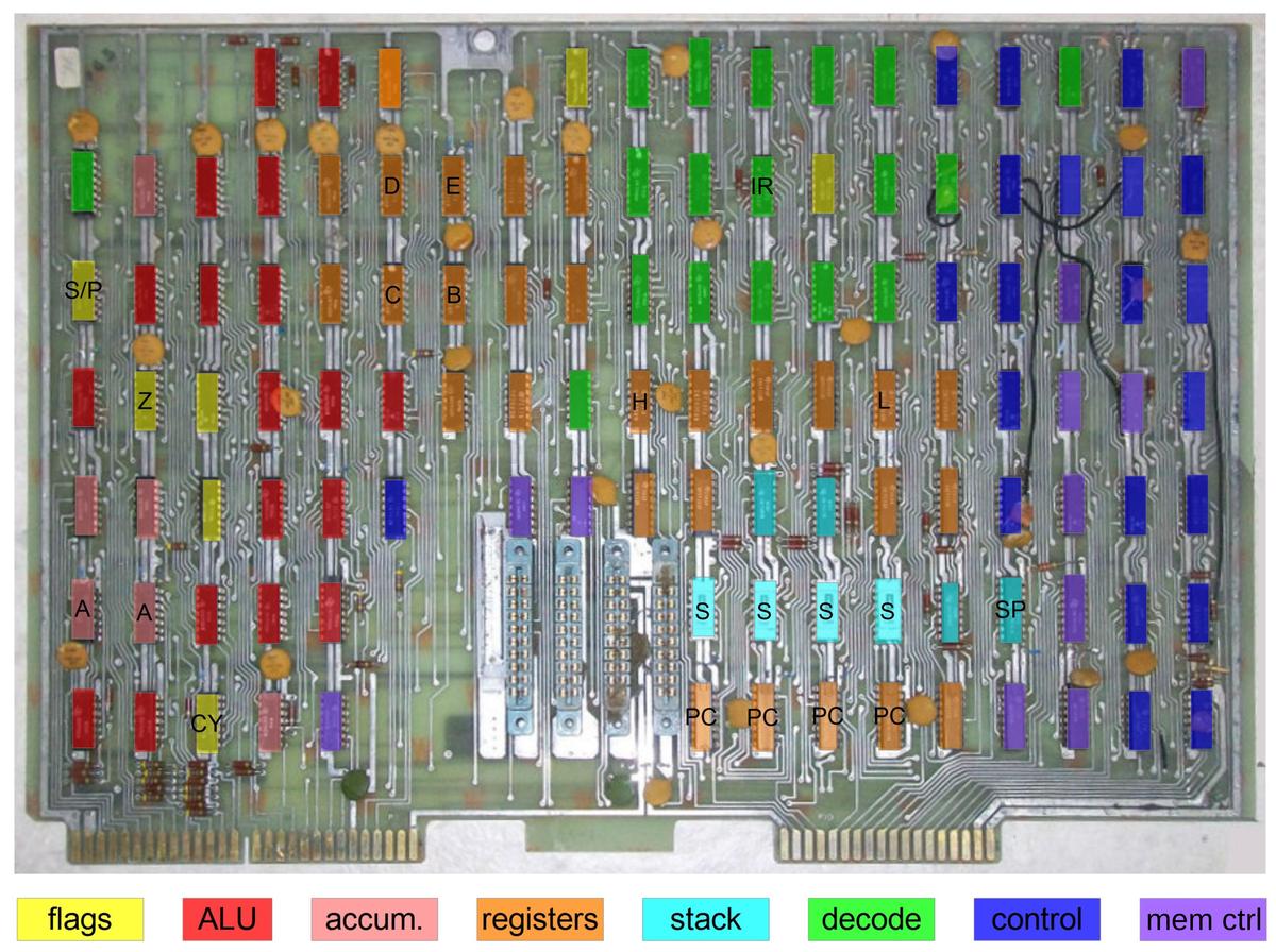
Since the Datapoint 2200 was designed before the creation of the microprocessor, its processor was built from a board of TTL chips (as was typical for minicomputers at the time). The diagram below shows the processor board with the chips categorized by function. The board has a separate chip for each 8-bit register (B, C, D, etc.) and separate chips for control flags (Z, carry, etc.). The Arithmetic/Logic Unit (ALU) takes about 18 chips, while instruction decoding is another 18 chips. Because every feature required more chips, the designers of the Datapoint 2200 were strongly motivated to make the instruction set as simple as possible. This was necessary since the Datapoint 2200 was a low-cost device, renting for just $148 a month. In contrast, the popular PDP-8 minicomputer rented for $500 a month.

The Datapoint 2200 processor board with registers, flags, and other blocks labeled. Click this image (or any other) for a larger version.
The Datapoint 2200 processor board with registers, flags, and other blocks labeled. Click this image (or any other) for a larger version.
One way that the Datapoint 2200 simplified the hardware was by creating a large set of instructions by combining simpler pieces in an orthogonal way. For instance, the Datapoint 2200 has 64 ALU instructions that apply one of eight ALU operations to one of the eight registers. This requires a small amount of hardware—eight ALU circuits and a circuit to select the register—but provides a large number of instructions. Another example is the register-to-register move instructions. Specifying one of eight source registers and one of eight destination registers provides a large, flexible set of instructions to move data.

The Datapoint 2200's instruction format was designed around this principle, with groups of three bits specifying a register. A common TTL chip could decode the group of three bits and activate the desired circuit.3 For instance, a data move instruction had the bit pattern 11DDDSSS to move a byte from the specified source (SSS) to the specified destination (DDD). (Note that this bit pattern maps onto three octal digits very nicely since the source and destination are separate digits.4)

One unusual feature of the Datapoint instruction set is that a memory access was just like a register access. That is, an instruction could specify one of the seven physical registers or could specify a memory access (M), using the identical instruction format. One consequence of this is that you couldn't include a memory address in an instruction. Instead, memory could only be accessed by first loading the address into the H and L registers, which held the high and low byte of the address respectively.5 This is very unusual and inconvenient, since a memory access took three instructions: two to load the H and L registers and one to access memory as the M "register". The advantage was that it simplified the instruction set and the decoding logic, saving chips and thus reducing the system cost. This decision also had lasting impact on Intel processors and how they access memory.

The table below shows the Datapoint 2200's instruction set in an octal table showing the 256 potential opcodes.6 I have roughly classified the instructions as arithmetic/logic (purple), control-flow (blue), data movement (green), input/output (orange), and miscellaneous (yellow). Note how the orthogonal instruction format produces large blocks of related instructions. The instructions in the lower right (green) load (L) a value from a source to a destination. (The no-operation NOP and HALT instructions are special cases.7) In the upper-left are Load operations (LA, etc.) that use an "immediate" byte, a data byte that follows the instruction. They use the same DDD code to specify the destination register, reusing that circuitry.

 0123456701234567
0HALTHALTSLCRFCAD LARETURNJFCINPUTCFC JMP CALL 
1  SRCRFZAC LB JFZ CFZ     
2   RFSSU LC JFSEX ADRCFSEX STATUS EX DATA EX WRITE
3   RFPSB LD JFPEX COM1CFPEX COM2 EX COM3 EX COM4
4   RTCND LE JTC CTC     
5   RTZXR LH JTZEX BEEPCTZEX CLICK EX DECK1 EX DECK2
6   RTSOR LL JTSEX RBKCTSEX WBK   EX BSP
7   RTPCP   JTPEX SFCTPEX SB EX REWND EX TSTOP
0ADAADBADCADDADEADHADLADMNOPLABLACLADLAELAHLALLAM
1ACAACBACCACDACEACHACLACMLBALBBLBCLBDLBELBHLBLLBM
2SUASUBSUCSUDSUESUHSULSUMLCALCBLCCLCDLCELCHLCLLCM
3SBASBBSBCSBDSBESBHSBLSBMLDALDBLDCLDDLDELDHLDLLDM
4NDANDBNDCNDDNDENDHNDLNDMLEALEBLECLEDLEELEHLELLEM
5XRAXRBXRCXRDXREXRHXRLXRMLHALHBLHCLHDLHELHHLHLLHM
6ORAORBORCORDOREORHORLORMLLALLBLLCLLDLLELLHLLLLLM
7CPACPBCPCCPDCPECPHCPLCPMLMALMBLMCLMDLMELMHLMLHALT

The lower-left quadrant (purple) has the bulk of the ALU instructions. These instructions have a regular, orthogonal structure making the instructions easy to decode: each row specifies the operation while each column specifies the source. This is due to the instruction structure: eight bits in the pattern 10AAASSS, where the AAA bits specified the ALU operation and the SSS bits specified the register source. The three-bit ALU code specifies the operations Add, Add with Carry, Subtract, Subtract with Borrow, logical AND, logical XOR, logical OR, and Compare. This list is important because it defined the fundamental ALU operations for later Intel processors.8 In the upper-left are ALU operations that use an "immediate" byte. These instructions use the same AAA bit pattern to select the ALU operation, reusing the decoding hardware. Finally, the shift instructions SLC and SRC are implemented as special cases outside the pattern.

The upper columns contain conditional instructions in blue—Return, Jump, and Call. The eight conditions test the four status flags (Carry, Zero, Sign, and Parity) for either True or False. (For example, JFZ Jumps if the Zero flag is False.) A 3-bit field selects the condition, allowing it to be easily decoded in hardware. The parity flag is somewhat unusual because parity is surprisingly expensive to compute in hardware, but because the Datapoint 2200 operated as a terminal, parity computation was important.

The Datapoint 2200 has an input instruction as well as many output instructions for a variety of specific hardware tasks (orange, labeled EX for external). Typical operations are STATUS to get I/O status, BEEP and CLICK to make sound, and REWIND to rewind the tape. As a result of this decision to use separate I/O instructions, Intel processors still use I/O instructions operating in an I/O space, different from processors such as the MOS 6502 and the Motorola 68000 that used memory-mapped I/O.

To summarize, the Datapoint 2200 has a fairly large number of instructions, but they are generated from about a dozen simple patterns that are easy to decode.9 By combining orthogonal bit fields (e.g. 8 ALU operations multiplied by 8 source registers), 64 instructions can be generated from one underlying pattern.

Intel 8008

The Intel 8008 was created as a clone of the Datapoint 2200 processor.10 Around the end of 1969, the Datapoint company talked with Intel and Texas Instruments about the possibility of replacing the processor board with a single chip. Even though the microprocessor didn't exist at this point, both companies said they could create such a chip. Texas Instruments was first with a chip called the TMX 1795 that they advertised as a "CPU on a chip". Slightly later, Intel produced the 8008 microprocessor. Both chips copied the Datapoint 2200's instruction set architecture with minor changes.

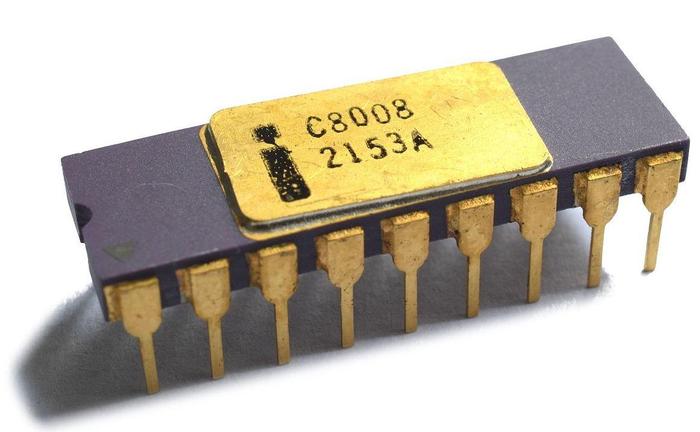
The Intel 8008 chip in its 18-pin package. The small number of pins hampered the performance of the 8008, but Intel was hesitant to even go to the 18-pin package. Photo by Thomas Nguyen, (CC BY-SA 4.0).

The Intel 8008 chip in its 18-pin package. The small number of pins hampered the performance of the 8008, but Intel was hesitant to even go to the 18-pin package. Photo by Thomas Nguyen, (CC BY-SA 4.0).

By the time the chips were completed, however, the Datapoint corporation had lost interest in the chips. They were designing a much faster version of the Datapoint 2200 with improved TTL chips (including the well-known 74181 ALU chip). Even the original Datapoint 2200 model was faster than the Intel 8008 processor, and the Version II was over 5 times faster,11 so moving to a single-chip processor would be a step backward.

Texas Instruments unsuccessfully tried to find a customer for their TMX 1795 chip and ended up abandoning the chip. Intel, however, marketed the 8008 as an 8-bit microprocessor, essentially creating the microprocessor industry. In my view, Intel's biggest innovation with the microprocessor wasn't creating a single-chip CPU, but creating the microprocessor as a product category: a general-purpose processor along with everything customers needed to take advantage of it. Intel put an enormous amount of effort into making microprocessors a success: from documentation and customer training to Intellec development systems, from support chips to software tools such as assemblers, compilers, and operating systems.

The table below shows the opcodes of the 8008. For the most part, the 8008 copies the Datapoint 2200, with identical instructions that have identical opcodes (in color). There are a few additional instructions (shown in white), though. Intel Designer Ted Hoff realized that increment and decrement instructions (IN and DC) would be very useful for loops. There are two additional bit rotate instructions (RAL and RAR) as well as the "missing" LMI (Load Immediate to Memory) instruction. The RST (restart) instructions act as short call instructions to fixed addresses for interrupt handling. Finally, the 8008 turned the Datapoint 2200's device-specific I/O instructions into 32 generic I/O instructions.

 0123456701234567
0HLTHLTRLCRFCADIRST 0LAIRETJFCINP 0CFCINP 1JMPINP 2CALINP 3
1INBDCBRRCRFZACIRST 1LBI JFZINP 4CFZINP 5 INP 6 INP 7
2INCDCCRALRFSSUIRST 2LCI JFSOUT 8CFSOUT 9 OUT 10 OUT 11
3INDDCDRARRFPSBIRST 3LDI JFPOUT 12CFPOUT 13 OUT 14 OUT 15
4INEDCE RTCNDIRST 4LEI JTCOUT 16CTCOUT 17 OUT 18 OUT 19
5INHDCH RTZXRIRST 5LHI JTZOUT 20CTZOUT 21 OUT 22 OUT 23
6INLDCL RTSORIRST 6LLI JTSOUT 24CTSOUT 25 OUT 26 OUT 27
7   RTPCPIRST 7LMI JTPOUT 28CTPOUT 29 OUT 30 OUT 31
0ADAADBADCADDADEADHADLADMNOPLABLACLADLAELAHLALLAM
1ACAACBACCACDACEACHACLACMLBALBBLBCLBDLBELBHLBLLBM
2SUASUBSUCSUDSUESUHSULSUMLCALCBLCCLCDLCELCHLCLLCM
3SBASBBSBCSBDSBESBHSBLSBMLDALDBLDCLDDLDELDHLDLLDM
4NDANDBNDCNDDNDENDHNDLNDMLEALEBLECLEDLEELEHLELLEM
5XRAXRBXRCXRDXREXRHXRLXRMLHALHBLHCLHDLHELHHLHLLHM
6ORAORBORCORDOREORHORLORMLLALLBLLCLLDLLELLHLLLLLM
7CPACPBCPCCPDCPECPHCPLCPMLMALMBLMCLMDLMELMHLMLHLT

Intel 8080

The 8080 improved the 8008 in many ways, focusing on speed and ease of use, and resolving customer issues with the 8008.12 Customers had criticized the 8008 for its small memory capacity, low speed, and difficult hardware interfacing. The 8080 increased memory capacity from 16K to 64K and was over an order of magnitude faster than the 8008. The 8080 also moved to a 40-pin package that made interfacing easier, but the 8080 still required a large number of support chips to build a working system.

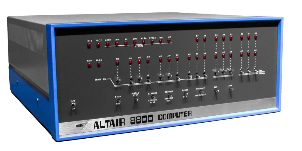
Although the 8080 was widely used in embedded systems, it is more famous for its use in the first generation of home computers, boxes such as the Altair and IMSAI. Famed chip designer Federico Faggin said that the 8080 really created the microprocessor; the 4004 and 8008 suggested it, but the 8080 made it real.13

Altair 8800 computer on display at the Smithsonian. Photo by Colin Douglas, (CC BY-SA 2.0).

Altair 8800 computer on display at the Smithsonian. Photo by Colin Douglas, (CC BY-SA 2.0).

The table below shows the instruction set for the 8080. The 8080 was designed to be compatible with 8008 assembly programs after a simple translation process; the instructions have been shifted around and the names have changed.15 The instructions from the Datapoint 2200 (colored) form the majority of the 8080's instruction set. The instruction set was expanded by adding some 16-bit support, allowing register pairs (BC, DE, HL) to be used as 16-bit registers for double add, 16-bit increment and decrement, and 16-bit memory transfers. Many of the new instructions in the 8080 may seem like contrived special cases— for example, SPHL (Load SP from HL) and XCHG (Exchange DE and HL)— but they made accesses to memory easier. The I/O instructions from the 8008 have been condensed to just IN and OUT, opening up room for new instructions.

 0123456701234567
0NOPLXI BSTAX BINX BINR BDCR BMVI BRLCMOV B,BMOV B,CMOV B,DMOV B,EMOV B,HMOV B,LMOV B,MMOV B,A
1 DAD BLDAX BDCX BINR CDCR CMVI CRRCMOV C,BMOV C,CMOV C,DMOV C,EMOV C,HMOV C,LMOV C,MMOV C,A
2 LXI DSTAX DINX DINR DDCR DMVI DRALMOV D,BMOV D,CMOV D,DMOV D,EMOV D,HMOV D,LMOV D,MMOV D,A
3 DAD DLDAX DDCX DINR EDCR EMVI ERARMOV E,BMOV E,CMOV E,DMOV E,EMOV E,HMOV E,LMOV E,MMOV E,A
4 LXI HSHLDINX HINR HDCR HMVI HDAAMOV H,BMOV H,CMOV H,DMOV H,EMOV H,HMOV H,LMOV H,MMOV H,A
5 DAD HLHLDDCX HINR LDCR LMVI LCMAMOV L,BMOV L,CMOV L,DMOV L,EMOV L,HMOV L,LMOV L,MMOV L,A
6 LXI SPSTAINX SPINR MDCR MMVI MSTCMOV M,BMOV M,CMOV M,DMOV M,EMOV M,HMOV M,LHLTMOV M,A
7 DAD SPLDADCX SPINR ADCR AMVI ACMCMOV A,BMOV A,CMOV A,DMOV A,EMOV A,HMOV A,LMOV A,MMOV A,A
0ADD BADD CADD DADD EADD HADD LADD MADD ARNZPOP BJNZJMPCNZPUSH BADIRST 0
1ADC BADC CADC DADC EADC HADC LADC MADC ARZRETJZ CZCALLACIRST 1
2SUB BSUB CSUB DSUB ESUB HSUB LSUB MSUB ARNCPOP DJNCOUTCNCPUSH DSUIRST 2
3SBB BSBB CSBB DSBB ESBB HSBB LSBB MSBB ARC JCINCC SBIRST 3
4ANA BANA CANA DANA EANA HANA LANA MANA ARPOPOP HJPOXTHLCPOPUSH HANIRST 4
5XRA BXRA CXRA DXRA EXRA HXRA LXRA MXRA ARPEPCHLJPEXCHGCPE XRIRST 5
6ORA BORA CORA DORA EORA HORA LORA MORA ARPPOP PSWJPDICPPUSH PSWORIRST 6
7CMP BCMP CCMP DCMP ECMP HCMP LCMP MCMP ARMSPHLJMEICM CPIRST 7

The 8080 also moved the stack to external memory, rather than using an internal fixed special-purpose stack as in the 8008 and Datapoint 2200. This allowed PUSH and POP instructions to put register data on the stack. Interrupt handling was also improved by adding the Enable Interrupt and Disable Interrupt instructions (EI and DI).14

Intel 8085

The Intel 8085 was designed as a "mid-life kicker" for the 8080, providing incremental improvements while maintaining compatibility. From the hardware perspective, the 8085 was much easier to use than the 8080. While the 8080 required three voltages, the 8085 required a single 5-volt power supply (represented by the "5" in the part number). Moreover, the 8085 eliminated most of the support chips required with the 8080; a working 8085 computer could be built with just three chips. Finally, the 8085 provided additional hardware functionality: better interrupt support and serial I/O.

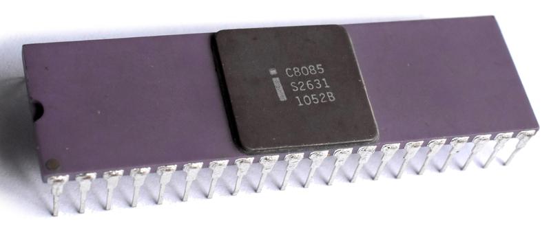
The Intel 8085, like the 8080 and the 8086, was packaged in a 40-pin DIP. Photo by Thomas Nguyen, (CC BY-SA 4.0).

The Intel 8085, like the 8080 and the 8086, was packaged in a 40-pin DIP. Photo by Thomas Nguyen, (CC BY-SA 4.0).

On the software side, the 8085 is curious: 12 instructions were added to the instruction set (finally using every opcode), but all but two were hidden and left undocumented.16 Moreover, the 8085 added two new condition codes, but these were also hidden. This situation occurred because the 8086 project started up in 1976, near the release of the 8085 chip. Intel wanted the 8086 to be compatible (to some extent) with the 8080 and 8085, but providing new instructions in the 8085 would make compatibility harder. It was too late to remove the instructions from the 8085 chip, so Intel did the next best thing and removed them from the documentation. These instructions are shown in red in the table below. Only the new SIM and RIM instructions were supported, necessary in order to use the 8085's new interrupt and serial I/O features.

 0123456701234567
0NOPLXI BSTAX BINX BINR BDCR BMVI BRLCMOV B,BMOV B,CMOV B,DMOV B,EMOV B,HMOV B,LMOV B,MMOV B,A
1DSUBDAD BLDAX BDCX BINR CDCR CMVI CRRCMOV C,BMOV C,CMOV C,DMOV C,EMOV C,HMOV C,LMOV C,MMOV C,A
2ARHLLXI DSTAX DINX DINR DDCR DMVI DRALMOV D,BMOV D,CMOV D,DMOV D,EMOV D,HMOV D,LMOV D,MMOV D,A
3RDELDAD DLDAX DDCX DINR EDCR EMVI ERARMOV E,BMOV E,CMOV E,DMOV E,EMOV E,HMOV E,LMOV E,MMOV E,A
4RIMLXI HSHLDINX HINR HDCR HMVI HDAAMOV H,BMOV H,CMOV H,DMOV H,EMOV H,HMOV H,LMOV H,MMOV H,A
5LDHIDAD HLHLDDCX HINR LDCR LMVI LCMAMOV L,BMOV L,CMOV L,DMOV L,EMOV L,HMOV L,LMOV L,MMOV L,A
6SIMLXI SPSTAINX SPINR MDCR MMVI MSTCMOV M,BMOV M,CMOV M,DMOV M,EMOV M,HMOV M,LHLTMOV M,A
7LDSIDAD SPLDADCX SPINR ADCR AMVI ACMCMOV A,BMOV A,CMOV A,DMOV A,EMOV A,HMOV A,LMOV A,MMOV A,A
0ADD BADD CADD DADD EADD HADD LADD MADD ARNZPOP BJNZJMPCNZPUSH BADIRST 0
1ADC BADC CADC DADC EADC HADC LADC MADC ARZRETJZRSTVCZCALLACIRST 1
2SUB BSUB CSUB DSUB ESUB HSUB LSUB MSUB ARNCPOP DJNCOUTCNCPUSH DSUIRST 2
3SBB BSBB CSBB DSBB ESBB HSBB LSBB MSBB ARCSHLXJCINCCJNKSBIRST 3
4ANA BANA CANA DANA EANA HANA LANA MANA ARPOPOP HJPOXTHLCPOPUSH HANIRST 4
5XRA BXRA CXRA DXRA EXRA HXRA LXRA MXRA ARPEPCHLJPEXCHGCPELHLXXRIRST 5
6ORA BORA CORA DORA EORA HORA LORA MORA ARPPOP PSWJPDICPPUSH PSWORIRST 6
7CMP BCMP CCMP DCMP ECMP HCMP LCMP MCMP ARMSPHLJMEICMJKCPIRST 7

Intel 8086

Following the 8080, Intel intended to revolutionize microprocessors with a 32-bit "micro-mainframe", the iAPX 432. This extremely complex processor implemented objects, memory management, interprocess communication, and fine-grained memory protection in hardware. The iAPX 432 was too ambitious and the project fell behind schedule, leaving Intel vulnerable against competitors such as Motorola and Zilog. Intel quickly threw together a 16-bit processor as a stopgap until the iAPX 432 was ready; to show its continuity with the 8-bit processor line, this processor was called the 8086. The iAPX 432 ended up being one of the great disaster stories of modern computing and quietly disappeared.

The "stopgap" 8086 processor, however, started the x86 architecture that changed the history of Intel. The 8086's victory was powered by the IBM PC, designed in 1981 around the Intel 8088, a variant of the 8086 with a cheaper 8-bit bus. The IBM PC was a rousing success, defining the modern computer and making Intel's fortune. Intel produced a succession of more powerful chips that extended the 8086: 286, 386, 486, Pentium, and so on, leading to the current x86 architecture.

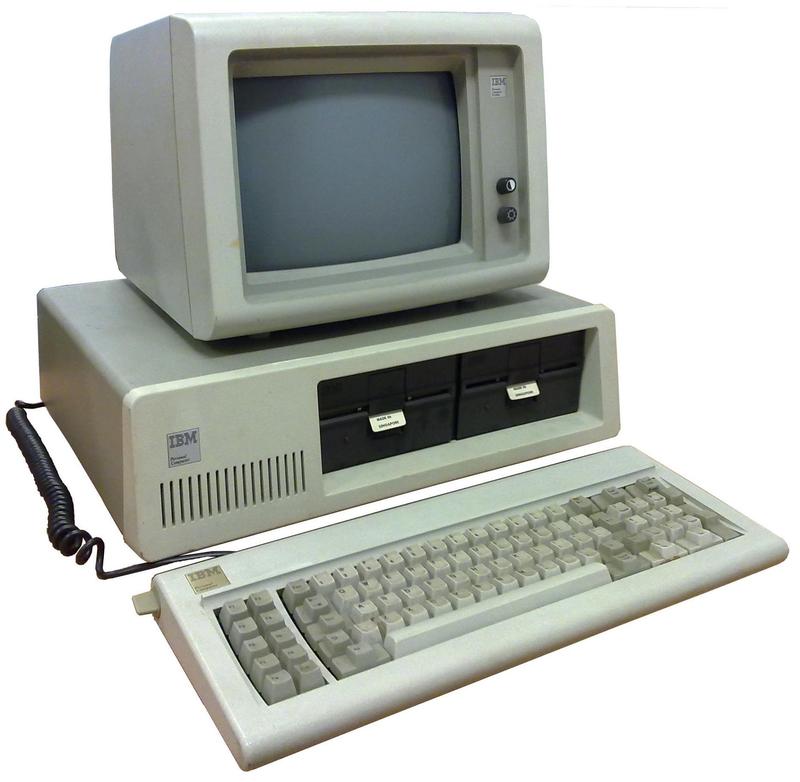
The original IBM PC used the Intel 8088 processor, a variant of the 8086 with an 8-bit bus. Photo by Ruben de Rijcke, (CC BY-SA 3.0).

The original IBM PC used the Intel 8088 processor, a variant of the 8086 with an 8-bit bus. Photo by Ruben de Rijcke, (CC BY-SA 3.0).

The 8086 was a major change from the 8080/8085, jumping from an 8-bit architecture to a 16-bit architecture and expanding from 64K of memory to 1 megabyte. Nonetheless, the 8086's architecture is closely related to the 8080. The designers of the 8086 wanted it to be compatible with the 8080/8085, but the difference was too wide for binary compatibility or even assembly-language compatibility. Instead, the 8086 was designed so a program could translate 8080 assembly language to 8086 assembly language.17 To accomplish this, each 8080 register had a corresponding 8086 register and most 8080 instructions had corresponding 8086 instructions.

The 8086's instruction set was designed with a new concept, the "ModR/M" byte, which usually follows the opcode byte. The ModR/M byte specifies the memory addressing mode and the register (or registers) to use, allowing that information to be moved out of the opcode. For instance, where the 8080 had a quadrant of 64 instructions to move from register to register, the 8086 has a single move instruction, with the ModR/M byte specifying the particular instruction. (The move instruction, however, has variants to handle byte vs. word operations, moves to or from memory, and so forth, so the 8086 ends up with a few move opcodes.) The ModR/M byte preserves the Datapoint 2200's concept of using the same instruction for memory and register operations, but allows a memory address to be provided in the instruction.

The 8086 also cleans up some of the historical baggage in the instruction set, freeing up space in the precious 256 opcodes for new instructions. The conditional call and return instructions were eliminated, while the conditional jumps were expanded. The 8008's RST (Restart) instructions were eliminated, replaced by interrupt vectors.

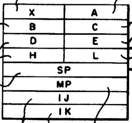
The 8086 extended its registers to 16 bits and added several new registers. An Intel patent (below) shows that the 8086's registers were originally called A, B, C, D, E, H, and L, matching the Datapoint 2200. The A register was extended to the 16-bit XA register, while the BC, DE, and HL registers were used unchanged. When the 8086 was released, these registers were renamed to AX, CX, DX, and BX respectively.18 In particular, the HL register was renamed to BX; this is why BX can specify a memory address in the ModR/M byte, but AX, CX, and DX can't.

A patent diagram showing the 8086's registers with their original names.  (MP, IJ, and IK are now known as BP, SI, and DI.) From patent US4449184.

A patent diagram showing the 8086's registers with their original names. (MP, IJ, and IK are now known as BP, SI, and DI.) From patent US4449184.

The table below shows the 8086's instruction set, with "b", "w", and "i" indicating byte (8-bit), word (16-bit), and immediate instructions. The Datapoint 2200 instructions (colored) are all still supported. The number of Datapoint instructions looks small because the ModR/M byte collapses groups of old opcodes into a single new one. This opened up space in the opcode table, though, allowing the 8086 to have many new instructions as well as 16-bit instructions.19

 0123456701234567
0ADD bADD wADD bADD wADD biADD wiPUSH ESPOP ESINC AXINC CXINC DXINC BXINC SPINC BPINC SIINC DI
1OR bOR wOR bOR wOR biOR wiPUSH CS DEC AXDEC CXDEC DXDEC BXDEC SPDEC BPDEC SIDEC DI
2ADC bADC wADC bADC wADC biADC wiPUSH SSPOP SSPUSH AXPUSH CXPUSH DXPUSH BXPUSH SPPUSH BPPUSH SIPUSH DI
3SBB bSBB wSBB bSBB wSBB biSBB wiPUSH DSPOP DSPOP AXPOP CXPOP DXPOP BXPOP SPPOP BPPOP SIPOP DI
4AND bAND wAND bAND wAND biAND wiES:DAA        
5SUB bSUB wSUB bSUB wSUB biSUB wiCS:DAS        
6XOR bXOR wXOR bXOR wXOR biXOR wiSS:AAAJOJNOJBJNBJZJNZJBEJA
7CMP bCMP wCMP bCMP wCMP biCMP wiDS:AASJSJNSJPEJPOJLJGEJLEJG
0GRP1 bGRP1 wGRP1 bGRP1 wTEST bTEST wXCHG bXCHG w  RETRETLESLDSMOV bMOV w
1MOV bMOV wMOV bMOV wMOV srLEAMOV srPOP  RETFRETFINT 3INTINTOIRET
2NOPXCHG CXXCHG DXXCHG BXXCHG SPXCHG BPXCHG SIXCHG DIShift bShift wShift bShift wAAMAAD XLAT
3CBWCWDCALLWAITPUSHFPOPFSAHFLAHFESC 0ESC 1ESC 2ESC 3ESC 4ESC 5ESC 6ESC 7
4MOV AL,MMOV AX,MMOV M,ALMOV M,AXMOVS bMOVS wCMPS bCMPS wLOOPNZLOOPZLOOPJCXZIN bIN wOUT bOUT w
5TEST bTEST wSTOS bSTOS wLODS bLODS wSCAS bSCAS wCALLJMPJMPJMPIN bIN wOUT b DXOUT w DX
6MOV AL,iMOV CL,iMOV DL,iMOV BL,iMOV AH,iMOV CH,iMOV DH,iMOV BH,iLOCK REPNZREPZHLTCMCGRP3aGRP3b
7MOV AX,iMOV CX,iMOV DX,iMOV BX,iMOV SP,iMOV BP,iMOV SI,iMOV DI,iCLCSTCCLISTICLDSTDGRP4GRP5

The 8086 has a 16-bit flags register, shown below, but the low byte remained compatible with the 8080. The four highlighted flags (sign, zero, parity, and carry) are the ones originating in the Datapoint 2200.

The flag word of the 8086 contains the original Datapoint 2200 registers.

The flag word of the 8086 contains the original Datapoint 2200 registers.

Modern x86 and x86-64

The modern x86 architecture has extended the 8086 to a 32-bit architecture (IA-32) and a 64-bit architecture (x86-6420), but the Datapoint features remain. At startup, an x86 processor runs in "real mode", which operates like the original 8086. More interesting is 64-bit mode, which has some major architectural changes. In 64-bit mode, the 8086's general-purpose registers are extended to sixteen 64-bit registers (and soon to be 32 registers). However, the original Datapoint registers are special and can still be accessed as byte registers within the corresponding 64-bit register; these are highlighted in the table below.21

General purpose registers in x86-64. From Intel Software Developer's Manual.

General purpose registers in x86-64. From Intel Software Developer's Manual.

The flag register of the 8086 was extended to 32 bits or 64 bits in x86. As the diagram below shows, the original Datapoint 2200 status flags are still there (highlighted in yellow).

The 32-bit and 64-bit flags of x86 contain the original Datapoint 2200 registers. From Intel Software Developer's Manual.

The 32-bit and 64-bit flags of x86 contain the original Datapoint 2200 registers. From Intel Software Developer's Manual.

The instruction set in x86 has been extended from the 8086, mostly through prefixes, but the instructions from the Datapoint 2200 are still there. The ModR/M byte was changed in 32-bit mode so the BX (originally HL) register is no longer special when accessing memory (although it's still special with 16-bit addressing, until Intel removes that in the upcoming x86-S simplification.) I/O ports still exist in x86, although they are viewed as more of a legacy feature: modern I/O devices typically use memory-mapped I/O instead of I/O ports. To summarize, fifty years later, x86-64 is slowly moving away from some of the Datapoint 2200 features, but they are still there.

Conclusions

The modern x86 architecture is descended from the Datapoint 2200's architecture. Because there is backward-compatibility at each step, you should theoretically be able to take a Datapoint 2200 binary, disassemble it to 8008 assembly, automatically translate it to 8080 assembly, automatically convert it to 8086 assembly, and then run it on a modern x86 processor. (The I/O devices would be different and cause trouble, of course.)

The Datapoint 2200's complete instruction set, its flags, and its little-endian architecture have persisted into current processors. This shows the critical importance of backward compatibility to customers. While Intel keeps attempting to create new architectures (iAPX 432, i960, i860, Itanium), customers would rather stay on a compatible architecture. Remarkably, Intel has managed to move from 8-bit computers to 16, 32, and 64 bits, while keeping systems mostly compatible. As a result, design decisions made for the Datapoint 2200 over 50 years ago are still impacting modern computers. Will processors still have the features of the Datapoint 2200 another fifty years from now? I wouldn't be surprised.22

Thanks to Joe Oberhauser for suggesting this topic. I plan to write more on the 8086, so follow me on Twitter @kenshirriff or RSS for updates. I've also started experimenting with Mastodon recently as @[email protected] so you can follow me there too.

Notes and references

  1. Shift-register memory was also used in the TV Typewriter (1973) and the display storage of the Apple I (1976). However, dynamic RAM (DRAM) rapidly dropped in price, making shift-register memory obsolete by the mid 1970s. (I wrote about the Intel 1405 shift register memory in detail in this article.) 

  2. For comparison, the popular PDP-8 minicomputer had just two main registers: the accumulator and a multiplier-quotient register; instructions typically operated on the accumulator and a memory location. The Data General Nova, a minicomputer released in 1969, had four accumulator / index registers. Mainframes generally had many more registers; the IBM System/360 (1964), for instance, had 16 general registers and four floating-point registers. 

  3. On the hardware side, instructions were decoded with BCD-to-decimal decoder chips (type 7442). These decoders normally decoded a 4-bit BCD value into one of 10 output lines. In the Datapoint 2200, they decoded a 3-bit value into one of 8 output lines, and the other two lines were ignored. This allowed the high-bit line to be used as a selection line; if it was set, none of the 8 outputs would be active. 

  4. These bit patterns map cleanly onto octal, so the opcodes are clearest when specified in octal. This octal structure has persisted in Intel processors including modern x86 processors. Unfortunately, Intel invariably specifies the opcodes in hexadecimal rather than octal, which obscures the underlying structure. This structure is described in detail in The 80x86 is an Octal Machine

  5. It is unusual for an instruction set to require memory addresses to be loaded into a register in order to access memory. This technique was common in microcode, where memory addresses were loaded into the Memory Address Register (MAR). As pwg pointed out, the CDC mainframes (e.g. 6600) had special address registers; when you changed an address register, the specified memory location was read or written to the corresponding operand register automatically.

    At first, I thought that serial memory might motivate the use of an address register, but I don't think there's a connection. Most likely, the Datapoint 2200 used these techniques to create a simple, orthogonal instruction set that was easy to decode, and they weren't particularly concerned with performance. 

  6. The instruction tables in this article are different from most articles, because I use octal instead of hexadecimal. (Displaying an octal-based instruction in a hexadecimal table obscures much of the underlying structure.) To display the table in octal, I break it into four quadrants based on the top octal digit of a three-digit opcode: 0, 1, 2, or 3. The digit 0-7 along the left is the middle octal digit and the digit along the top is the low octal digit. 

  7. The regular pattern of Load instructions is broken by the NOP and HALT instructions. All the register-to-register load instructions along the diagonal accomplish nothing since they move a register to itself, but only the first one is explicitly called NOP. Moving a memory location to itself doesn't make sense, so its opcode is assigned the HALT instruction. Note that the all-0's opcode and the all-1's opcode are both HALT instructions. This is useful since it can stop execution if the program tries executing uninitialized memory. 

  8. You might think that Datapoint and Intel used the same ALU operations simply because they are the obvious set of 8 operations. However, if you look at other processors around that time, they use a wide variety of ALU operations. Similarly, the status flags in the Datapoint 2200 aren't the obvious set; systems with four flags typically used Sign, Carry, Zero, and Overflow (not Parity). Parity is surprisingly expensive to implement on a standard processor, but (as Philip Freidin pointed out) parity is cheap on a serial processor like the Datapoint 2200. Intel processors didn't provide an Overflow flag until the 8086; even the 8080 didn't have it although the Motorola 6800 and MOS 6502 did. The 8085 implemented an overflow flag (V) but it was left undocumented. 

  9. You might wonder if the Datapoint 2200 (and 8008) could be considered RISC processors since they have simple, easy-to-decode instruction sets. I think it is a mistake to try to wedge every processor into the RISC or CISC categories (Reduced Instruction Set Computer or Complex Instruction Set Computer). In particular, the Datapoint 2200 wasn't designed with the RISC philosophy (make a processor more powerful by simplifying the instruction set), its instruction set architecture is very different from RISC chips, and its implementation is different from RISC chips. Similarly, it wasn't designed with a CISC philosophy (make a processor more powerful by narrowing the semantic gap with high-level languages) and it doesn't look like a CISC chip.

    So where does that leave the Datapoint 2200? In "RISC: Back to the future?", famed computer architect Gordon Bell uses the term MISC (Minimal Instruction Set Computer) to describe the architecture of simple, early computers and microprocessors such as the Manchester Mark I (1948), the PDP-8 minicomputer (1966), and the Intel 4004 (1971). Computer architecture evolved from these early hardwired "simple computers" to microprogrammed processors, processors with cache, and hardwired, pipelined processors. "Minimal Instruction Set Computer" seems like a good description of the Datapoint 2200, since it is about the smallest, simplest processor that could get the job done. 

  10. Many people think that the Intel 8008 is an extension of the 4-bit Intel 4004 processor, but they are completely unrelated aside from the part numbers. The Intel 4004 is a 4-bit processor designed to implement a calculator for a company called Busicom. Its architecture is completely different from the 8008. In particular, the 4004 is a "Harvard architecture" system, with data storage and instruction storage completely separate. The 4004 also has a fairly strange instruction set, designed for calculators. For instance, it has a special instruction to convert a keyboard scan code to binary. The 4004 team and the 8008 team at Intel had many people in common, however, so the two chips have physical layouts (floorplans) that are very similar. 

  11. In this article, I'm focusing on the Datapoint 2200 Version I. Any time I refer to the Datapoint 2200, I mean the version I specifically. The Version II has an expanded instruction set, but it was expanded in an entirely different direction from the Intel 8080, so it's not relevant to this post. The Version II is interesting, however, since it provides a perspective of how the Intel 8080 could have developed in an "alternate universe". 

  12. Federico Faggin wrote The Birth of the Microprocessor in Byte Magazine, March 1992. This article describes in some detail the creation of the 8008 and 8080.

    The Oral History of the 8080 discusses many of the problems with the 8008 and how the 8080 addressed them. (See page 4.) Masatoshi Shima, one of the architects of the 4004, described five problems with the 8008: It was slow because it used two clock cycles per state. It had no general-purpose stack and was weak with interrupts. It had limited memory and I/O space. The instruction set was primitive, with only 8-bit data, limited addressing, and a single address pointer register. Finally, the system bus required a lot of interface circuitry. (See page 7.) 

  13. The 8080 is often said to be the "first truly usable microprocessor". Supposedly the source of this quote is Forgotten PC history, but the statement doesn't appear there. I haven't been able to find the original source of this statement, so let me know. In any case, I don't think that statement is particularly accurate, as the Motorola 6800 was "truly usable" and came out before the Intel 8080.

    The 8080 was first in one important way, though: it was Intel's first microprocessor that was designed with feedback from customers. Both the 4004 and the 8008 were custom chips for a single company. The 8080, however, was based on extensive customer feedback about the flaws in the 8008 and what features customers wanted. The 8080 oral history discusses this in more detail. 

  14. The 8008 was built with PMOS circuitry, while the 8080 was built with NMOS. This may seem like a trivial difference, but NMOS provided much superior performance. NMOS became the standard microprocessor technology until the rise of CMOS in the 1980s, combining NMOS and PMOS to dramatically reduce power consumption.

    Another key hardware improvement was that the 8080 used a 40-pin package, compared to the 18-pin package of the 8008. Intel had long followed the "religion" of small 16-pin packages, and only reluctantly moved to 18 pins (as in the 8008). However, by the time the 8080 was introduced, Intel recognized the utility of industry-standard 40-pin packages. The additional pins made the 8080 much easier to interface to a system. Moreover, the 8080's 16-bit address bus supported four times the memory of the 8008's 14-bit address bus. (The 40-pin package was still small for the time; some companies used 50-pin or 64-pin packages for microprocessors.) 

  15. The 8080 is not binary-compatible with the 8008 because almost all the instructions were shifted to different opcodes. One important but subtle change was that the 8 register/memory codes were reordered to start with B instead of A. The motivation is that this gave registers in a 16-bit register pair (BC, DE, or HL) codes that differ only in the low bit. This makes it easier to specify a register pair with a two-bit code. 

  16. Stan Mazor (one of the creators of the 4004 and 8080) explained that the 8085 removed 10 of the 12 new instructions because "they would burden the 8086 instruction set." Because the decision came near the 8085's release, they would "leave all 12 instructions on the already designed 8085 CPU chip, but document and announce only two of them" since modifying a CPU is hard but modifying a CPU's paper reference manual is easy.

    Several of the Intel 8086 engineers provided a similar explanation in Intel Microprocessors: 8008 to 8086: While the 8085 provided the new RIM and SIM instructions, "several other instructions that had been contemplated were not made available because of the software ramifications and the compatibility constraints they would place on the forthcoming 8086."

    For more information on the 8085's undocumented instructions, see Unspecified 8085 op codes enhance programming. The two new condition flags were V (2's complement overflow) and X5 (underflow on decrement or overflow on increment). The opcodes were DSUB (double (i.e. 16-bit) subtraction), ARHL (arithmetic shift right of HL), RDEL (rotate DE left through carry), LDHI (load DE with HL plus an immediate byte), LDSI (load DE with SP plus an immediate byte), RSTV (restart on overflow), LHLX (load HL indirect through DE), SHLX (store HL indirect through DE), JX5 (jump on X5), and JNX5 (jump on not X5). 

  17. Conversion from 8080 assembly code to 8086 assembly code was performed with a tool called CONV86. Each line of 8080 assembly code was converted to the corresponding line (or sometimes a few lines) of 8086 assembly code. The program wasn't perfect, so it was expected that the user would need to do some manual editing. In particular, CONV86 couldn't handle self-modifying code, where the program changed its own instructions. (Nowadays, self-modifying code is almost never used, but it was more common in the 1970s in order to make code smaller and get more performance.) CONV86 also didn't handle the 8085's RIM and SIM instructions, recommending a rewrite if code used these instructions heavily.

    Writing programs in 8086 assembly code manually was better, of course, since the program could take advantage of the 8086's new features. Moreover, a program converted by CONV86 might be 25% larger, due to the 8086's use of two-byte instructions and inefficiencies in the conversion. 

  18. This renaming is why the instruction set has the registers in the order AX, CX, DX, BX, rather than in alphabetical order as you might expect. The other factor is that Intel decided that AX, BX, CX, and DX corresponded to Accumulator, Base, Count, and Data, so they couldn't assign the names arbitrarily. 

  19. A few notes on how the 8086's instructions relate to the earlier machines, since the ModR/M byte and 8- vs. 16-bit instructions make things a bit confusing. For an instruction like ADD, I have three 8-bit opcodes highlighted: an add to memory/register, an add from memory/register, and an immediate add. The neighboring unhighlighted opcodes are the corresponding 16-bit versions. Likewise, for MOV, I have highlighted the 8-bit moves to/from a register/memory. 

  20. Since the x86's 32-bit architecture is called IA-32, you might expect that IA-64 would be the 64-bit architecture. Instead, IA-64 is the completely different architecture used in the ill-fated Itanium. IA-64 was supposed to replace IA-32, despite being completely incompatible. Since AMD was cut out of IA-64, AMD developed their own 64-bit extension of the existing x86 architecture and called it AMD64. Customers flocked to this architecture while the Itanium languished. Intel reluctantly copied the AMD64 architecture, calling it Intel 64. 

  21. The x86 architecture allows byte access to certain parts of the larger registers (accessing AL, AH, etc.) as well as word and larger accesses. These partial-width reads and writes to registers make the implementation of the processor harder due to register renaming. The problem is that writing to part of a register means that the register's value is a combination of the old and new values. The Register Alias Table in the P6 architecture deals with this by adding a size field to each entry. If you write a short value and then read a longer value, the pipeline stalls to figure out the right value. Moreover, some 16-bit code uses the two 8-bit parts of a register as independent registers. To support this, the Register Alias Table keeps separate entries for the high and low byte. (For details, see the book Modern Processor Design, in particular the chapter on Intel's P6 Microarchitecture.) The point of this is that obscure features of the Datapoint 2200 (such as H and L acting as a combined register) can cause implementation difficulties 50 years later. 

  22. Some miscellaneous references: For a detailed history of the Datapoint 2200, see Datapoint: The Lost Story of the Texans Who Invented the Personal Computer Revolution. The 8008 oral history provides a lot of interesting information on the development of the 8008. For another look at the Datapoint 2200 and instruction sets, see Comparing Datapoint 2200, 8008, 8080 and Z80 Instruction Sets