Reverse-engineering a vintage power supply chip from die photos

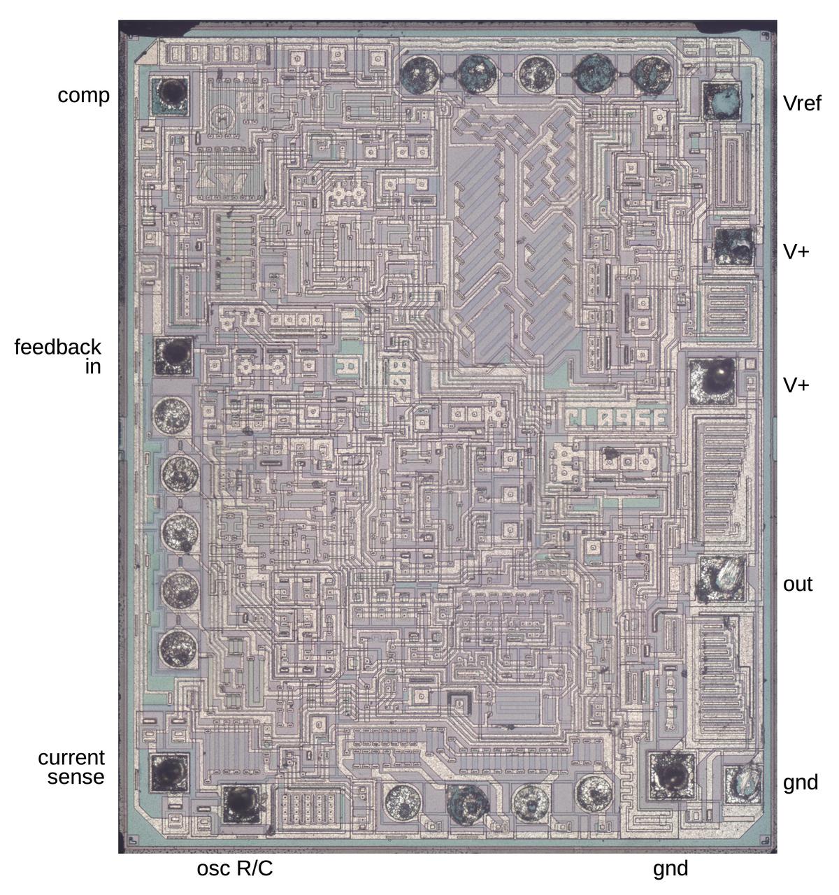
I recently did a PC power supply teardown so I figured it would be interesting to go deeper and see what happens inside the power supply's control IC. The die photo below shows the UC3842 chip, which was very popular in older PC power supplies.1 (The chip was introduced in 1984 but this die has a date of 2000.) The tiny silicon die is patterned to create the transistors, resistors and capacitors that make up the circuit. The lighter-colored lines are the metal layer on top of the silicon, forming the chip's wiring. Around the edges, square pads provide the connections from the die to the IC's external pins; tiny bond wires connect the pads to the chip's external pins.

The UC3842 die. Around the outside, the pins are labeled. (Click this image, or any other, for a larger version.)

The UC3842 die. Around the outside, the pins are labeled. (Click this image, or any other, for a larger version.)

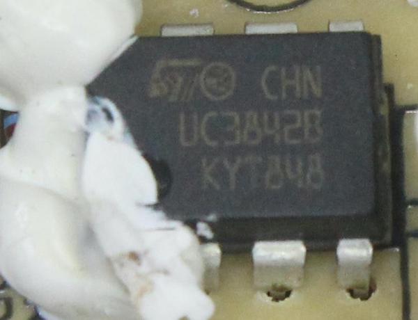
The photo below shows the chip mounted on the power supply board. For the die photos, I extracted the die from the epoxy package by heating it and then cleaned up the die with a few drops of sulfuric acid. I took photos with a microscope and stitched them together to create a high-resolution image.

The UC3842 chip mounted on the power supply's circuit board. The white glob is silicone, which held many of the power supply components in place.

The UC3842 chip mounted on the power supply's circuit board. The white glob is silicone, which held many of the power supply components in place.

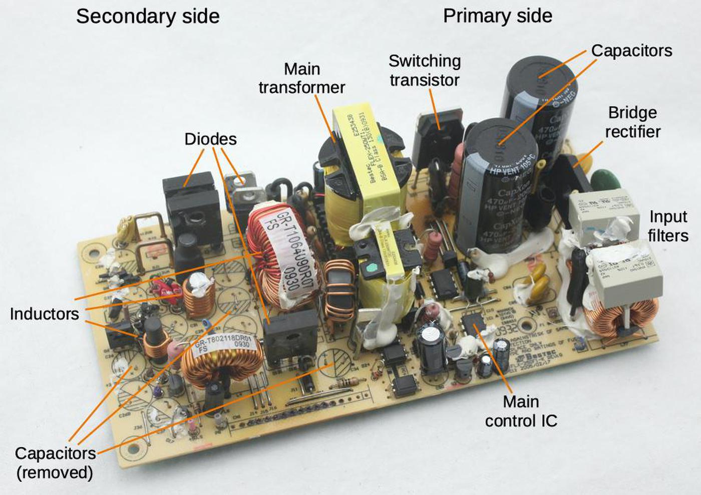
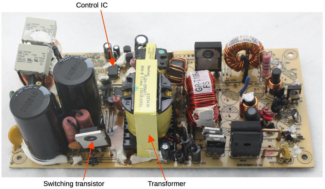
The chip is from the PC power supply below. This is a switching power supply so it uses several steps to produce the output voltages. On the primary side, the input AC is filtered and then converted to high-voltage DC (roughly 170 to 340 volts) by the bridge rectifier, and the large capacitors smooth it out. Next, the DC is chopped into pulses thousands of times a second by the switching transistor. The control IC constantly adjusts the width of the pulses to regulate the output voltage. These pulses go into the transformer, which converts the high-voltage pulses into low-voltage, high-current. The diodes on the secondary side produce the multiple DC outputs, which are smoothed by the inductors and capacitors.

An ATX power supply with the main components labeled. I removed the heat sinks and capacitors to improve visibility.

An ATX power supply with the main components labeled. I removed the heat sinks and capacitors to improve visibility.

This process may seem complex, but it has several advantages over putting the AC from the wall directly into a transformer. First, because the transformer operates at thousands of hertz instead of 60 hertz, a much smaller transformer can be used. Second, chopping the DC into pulses wastes very little energy, compared to a "linear regulator" that converts excess voltage into heat. The result is a power supply that is inexpensive, lightweight, and efficient.

In this blog post, I'll explain the construction of the controller IC, the building blocks of its circuitry, and how it operates. This may be a lot for one blog post, but we'll see how it goes.

Some silicon components

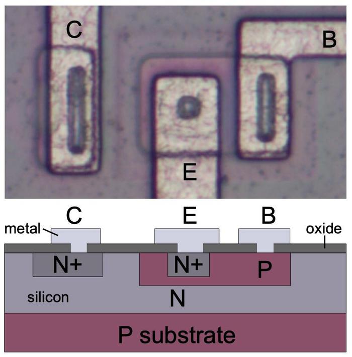
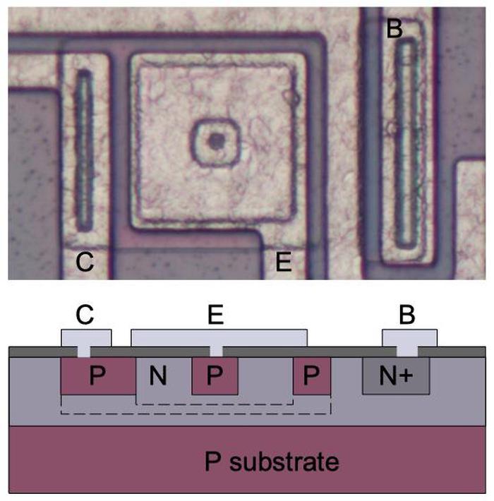
This IC is built from a type of transistor known as bipolar, rather than the MOS transistors that are typically used in modern ICs. The highly-magnified photo below shows an NPN transistor as it appears on the chip, with a cross-section drawing underneath. The metal wiring on top of the transistor is visible as the wide light-colored lines. Different regions of the silicon are doped with impurities to change its electrical properties, yielding N-type and P-type silicon. These regions are faintly visible in the photo. An oxide layer on top of the silicon provides insulation from the metal, except where a contact (black circle or oval) provides a connection between the metal and silicon.

Diagram illustrating the construction of an NPN transistor.

Diagram illustrating the construction of an NPN transistor.

The chip also uses many PNP transistors. Although you might expect a PNP transistor to simply be the reverse of an NPN transistor, it has a different structure, with the regions arranged laterally instead of vertically. The collector and base form concentric square rings around the emitter. The base wire is not connected to the base region directly. Instead, the wire is at a distance, and the base signal travels underneath through the N layer.

Diagram illustrating the construction of a PNP transistor. The dotted lines represent how the collector and base surround the emitter.

Diagram illustrating the construction of a PNP transistor. The dotted lines represent how the collector and base surround the emitter.

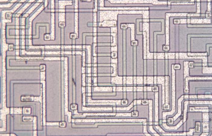
Because this chip consists of mostly analog circuitry, it uses a lot of resistors. The photo below shows several typical resistors, the thin grayish-green lines. The resistors are connected to metal wires at either end, the wider metallic-looking traces. Some resistors are straight lines, while others zig-zag to fit a longer resistor (i.e. higher resistance) into the available space.

Resistors on the die.

Resistors on the die.

Resistors are an inconvenient component for integrated circuits. First, they take up a relatively large amount of room, especially long, high-value resistors. Second, they are inaccurate; their value can vary unpredictably from chip to chip, or even on a single chip. For this reason, circuits are typically designed so they depend on the ratio between two resistors, which is much more stable.

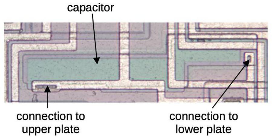
Capacitors are also bulky so the chip uses only a few, to stabilize its amplifiers. A capacitor can be formed by using the underlying silicon as one plate, and then putting a layer of polysilicon on top to form the second plate, separated by a thin layer of insulating oxide. Polysilicon is a special type of silicon, and appears green in the photo.

A capacitor on the die.

A capacitor on the die.

Architecture of the chip

To summarize the chip, it generates pulses to control the switching transistor that feeds the transformer. These pulses are at a fixed frequency (e.g. 52 kHz), but the width of the pulses increases if more power is needed to keep the output voltage constant. The chip constantly adjusts the pulse width based on voltage and current feedback from the power supply, keeping the output voltages stable even as the load changes.

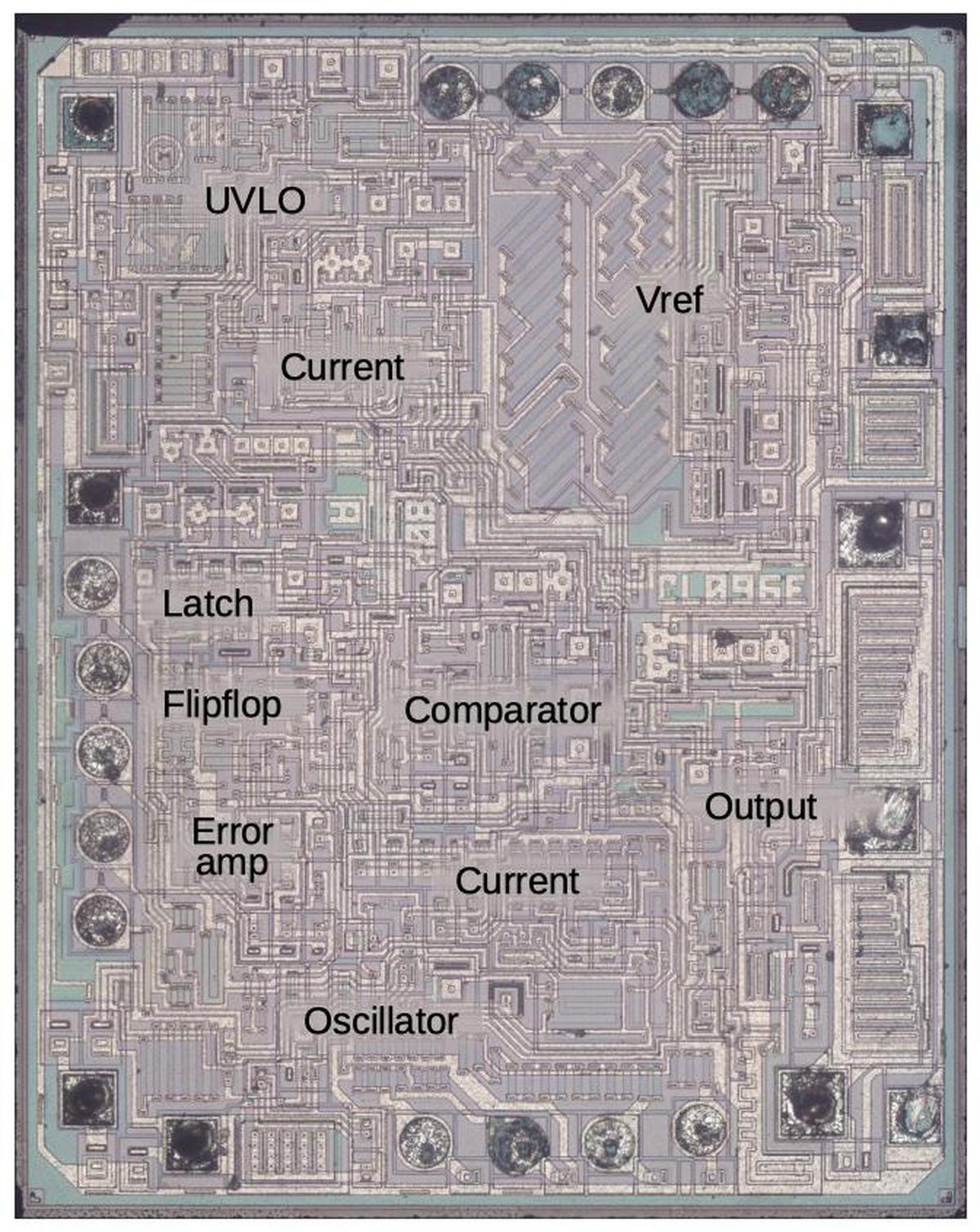
The UC3842 die. Main functional blocks of the die are labeled.

The UC3842 die. Main functional blocks of the die are labeled.

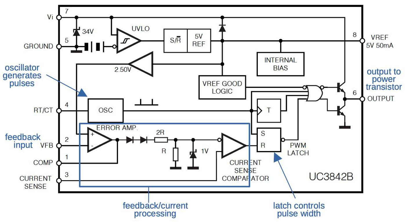
The die image above has been labeled with the main functional blocks of the chip. It can be compared with the block diagram (below) from the datasheet. I'll describe the main functional blocks before explaining how they are implemented.

Block diagram of the UC3842 chip with annotation. Original from the datasheet.

Block diagram of the UC3842 chip with annotation. Original from the datasheet.

The power supply's pulses start with the chip's oscillator, which generates pulses at a frequency controlled by an external resistor and capacitor. Below the oscillator is the feedback circuitry that adjusts the pulse width based on voltage and current feedback. The PWM latch (Pulse Width Modulation) combines the oscillator signal and the feedback to generate pulses of the right duration. These pulses go to the high-current output stage, which drives the external switching transistor.

The chip itself is powered by an auxiliary winding on the transformer that provides 15 to 30 volts. The chip regulates this down to an internal 5-volt supply, using a special circuit called a bandgap regulator to keep this voltage stable within 2%, even with changing temperature. (This regulated reference voltage is also provided externally as Vref for external circuitry that needs a stable voltage.)

A potential problem is that if the power supply is unplugged (for example), the chip may behave unpredictably as the input voltage drops. To guard against this, an Under-Voltage Lock Out (UVLO) feature shuts the chip down cleanly if the input drops too low.

A final interesting feature of the chip is how it starts up. As described above, the chip is powered by the transformer, but the chip generates the pulses that feed the transformer. This seems like a chicken-and-egg problem, since the chip won't receive any power until it is already driving the transformer. The solution is a connection to the rectified line voltage through a very large resistor, so the chip receives hundreds of volts but just microamps of current. A Zener diode (below) drops this startup voltage down to 34 volts, enough for the chip to start generating pulses, at which point the transformer takes over.2

The Zener diode on the chip. It limits the startup voltage to 34 volts. It consists of five diodes in series.

The Zener diode on the chip. It limits the startup voltage to 34 volts. It consists of five diodes in series.

The oscillator

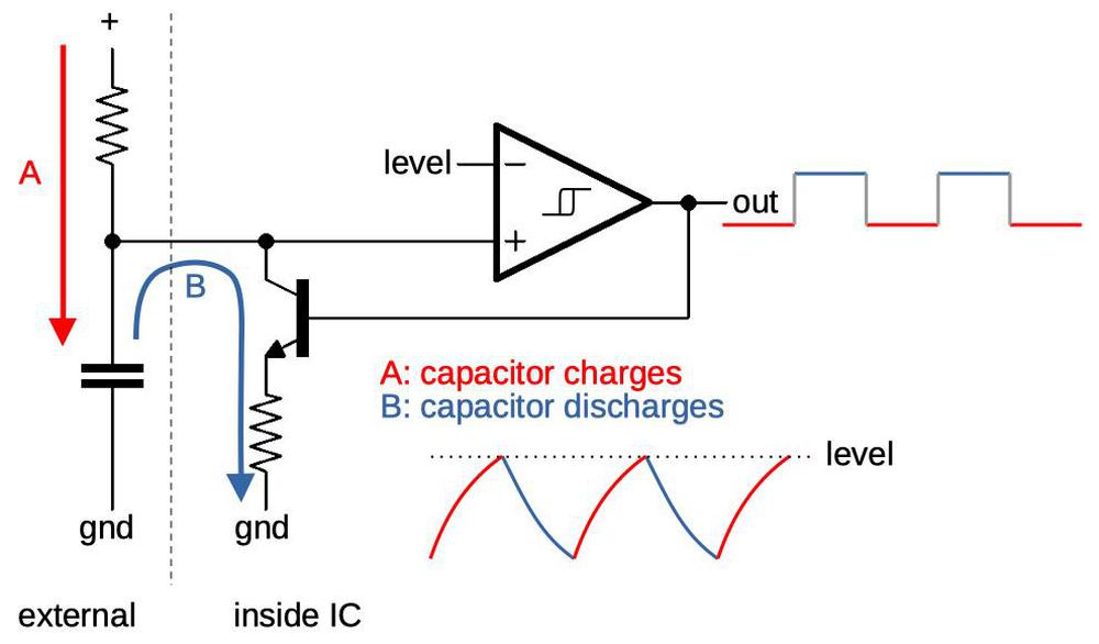
The simplified diagram below shows how the oscillator works. In the first phase (A), the external capacitor is charged through the resistor. When the voltage on the capacitor reaches a fixed level, the comparator (triangle) turns on, energizing the discharge transistor. In the next phase (B), the capacitor discharges through an internal resistor, and then the cycle starts again.3 Thus, by choosing particular values for the external resistor and capacitor, the power supply designer can select the oscillator frequency.

This diagram shows how the oscillator is controlled by an external resistor and capacitor.

This diagram shows how the oscillator is controlled by an external resistor and capacitor.

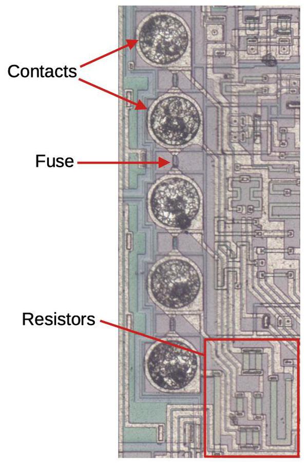
As mentioned earlier, resistors inside an IC are inaccurate. This poses a problem for the oscillator, since the discharge voltage level is set by resistors. The solution is to tune the resistances by putting fuses in parallel with small resistors and selectively blowing fuses to add the resistors to the circuit.4 Specifically, before the chip is packaged, its performance is measured. To blow a fuse, probes are pressed against the circular contacts and a large current is applied. The additional step of blowing fuses increases the manufacturing cost of the chip, but it provides more precise performance.

Fuses to adjust resistance.

Fuses to adjust resistance.

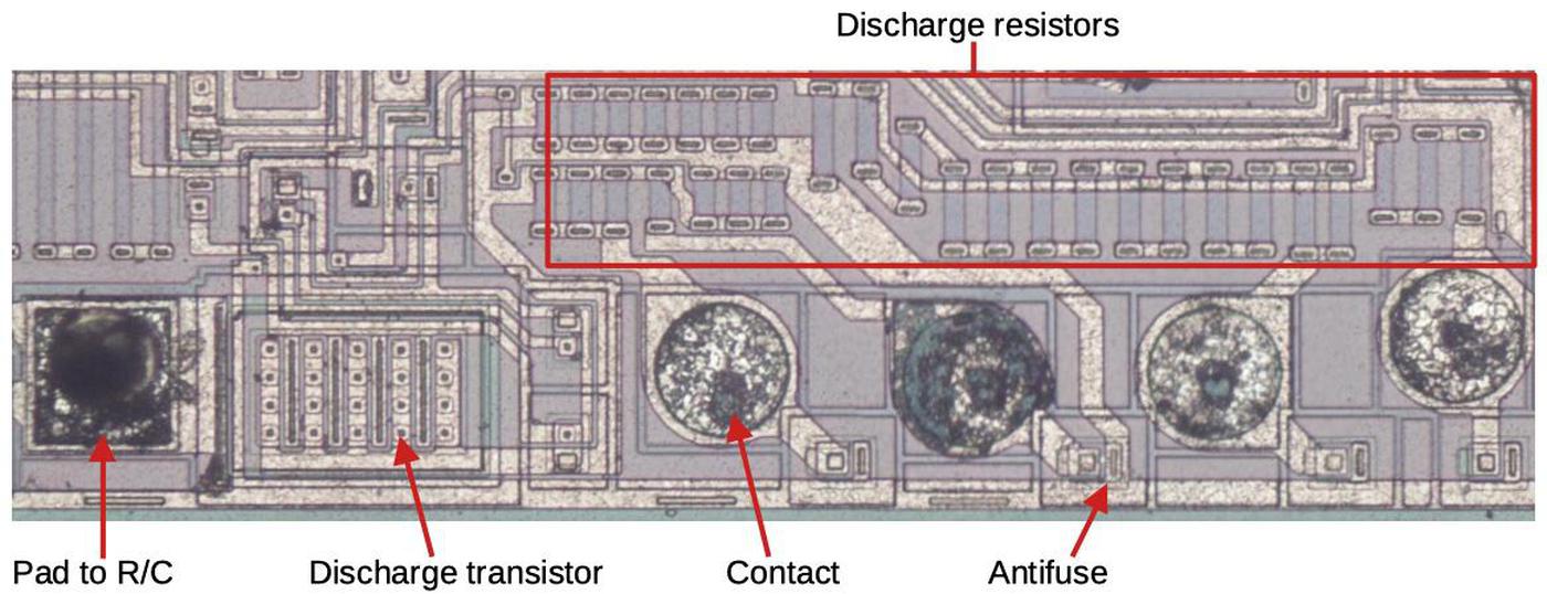
The oscillator has a second set of fuses to tune the discharge resistance (below). These fuses use a different principle: they are "antifuses", which act like fuses in reverse. An antifuse starts off non-conducting, but passing a high current through it creates a conductive metal spike in the antifuse.5

The discharge circuitry of the oscillator. The antifuses adjust resistance in the oscillator.

The discharge circuitry of the oscillator. The antifuses adjust resistance in the oscillator.

Current mirrors

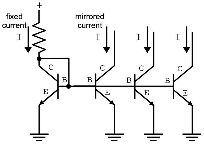
The current mirror is a fundamental building block in analog circuits. This chip, like many analog chips, needs small, steady currents to drive amplifiers, bias circuits, pull signals up, and perform other tasks. Rather than using separate resistors to generate each current, a common solution is the current mirror: you control one current with resistors, and then use transistors to make copies of this current. The schematic below shows a simple current mirror where the fixed current through the transistor on the left is mirrored into three identical copies.

A basic current mirror circuit. The current on the left is mirrored into three current sinks.

A basic current mirror circuit. The current on the left is mirrored into three current sinks.

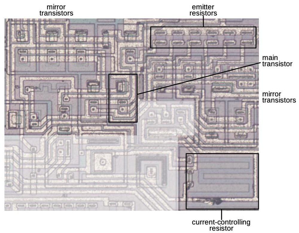
The diagram above shows the main current mirrors for the chip. The large resistor in the lower-right controls the current through the main transistor, and the other transistors copy this current.6 Small emitter resistors improve the performance.

The current-mirror circuitry on the die.

The current-mirror circuitry on the die.

The feedback or error amplifier

Next, I'll look at the voltage feedback circuit, which lets the chip know if the output voltage is too high or too low. The chip receives the output voltage, scaled to form a feedback signal. The error amplifier compares the feedback to a reference voltage to determine if the voltage is too high or too low.

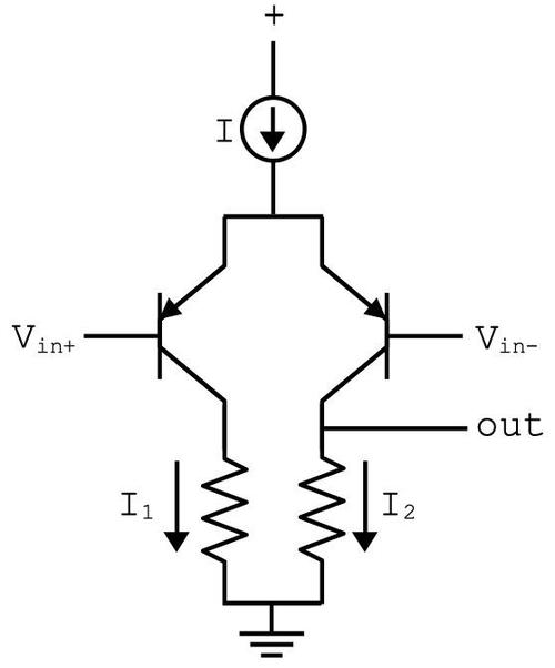
The error amplifier is based on a differential amplifier, which amplifies the difference between its two inputs. This circuit is common in analog circuits, forming the heart of an op-amp or a comparator. The basic idea is that a current mirror (the circle at the top) generates a fixed current I. This current gets split between the left path (I1) and the right path (I2). If the transistor on the left has a higher input voltage than the transistor on the right, most of the current will go to the left. But if the transistor on the right has a higher input, most of the current will go to the right. This circuit amplifies the voltage difference: even a small difference between the two inputs will switch most of the current from one side to the other.

A differential pair amplifies the difference between the two inputs.

A differential pair amplifies the difference between the two inputs.

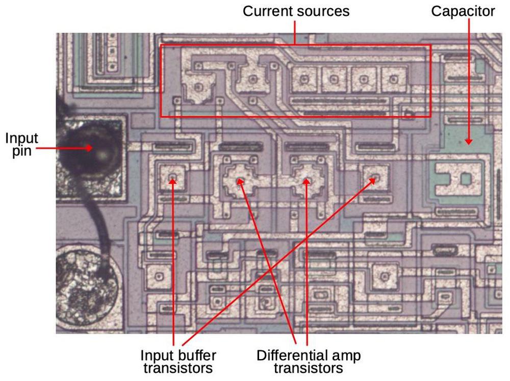
The error amplifier extends this circuit with about a dozen transistors in total. These transistors add buffering to the inputs, control various currents, and provide a second amplification stage. The photo below shows the key components of the error amplifier. The green capacitor on the right stabilizes the amplifier.

The error feedback amplifier as it appears on the die with key components indicated.

The error feedback amplifier as it appears on the die with key components indicated.

The current comparator

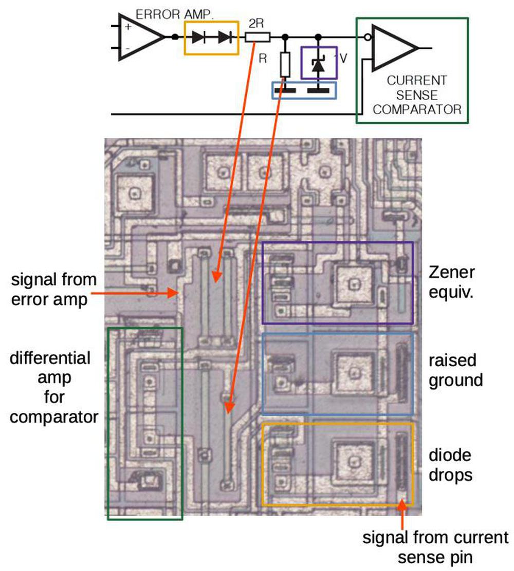
The power supply uses voltage feedback to adjust the pulse width, but it also monitors the current through the transformer so the power supply can respond faster to changes in the load. The current feedback is implemented by the "current sense comparator". This is similar to the feedback amplifier, amplifying the difference between the inputs. (Since it is a comparator, not an amplifier, it is designed to output a binary signal instead of an analog level, but the basic principle is the same.) The diagram below shows the key circuitry for the current comparator on the die and how it relates to the block diagram. The output from the error amplifier goes through some circuitry to adjust the voltage levels before entering the comparator.7

How the current sense circuit maps onto the die components.

How the current sense circuit maps onto the die components.

Under-voltage lockout

Another interesting circuit is the under-voltage lockout (UVLO), in the upper-left of the die. The purpose of this circuit is to shut down the chip cleanly if the input voltage falls too low. (This could happen if there is a power failure or even from unplugging the power supply.)

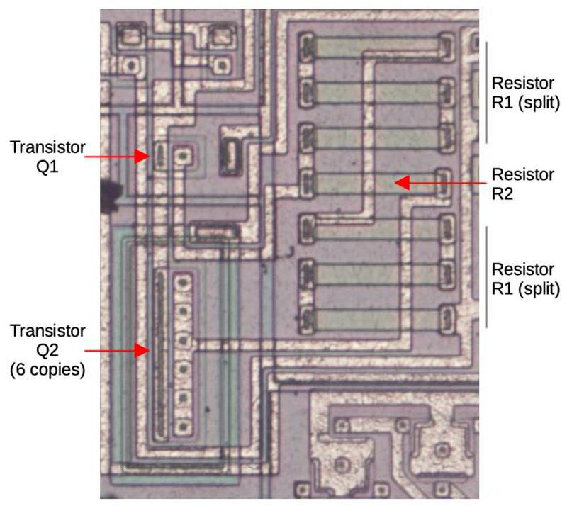
The heart of the UVLO circuit is a bandgap regulator, which provides a voltage reference that will be stable even if the temperature changes. This is surprisingly difficult in an integrated circuit, since the properties of transistors change with temperature. The bandgap regulator uses two transistors of different sizes so they are affected by temperature differently. In the die photo below, Q2 is six times the size of Q1.

The bandgap circuit for the under-voltage lockout.

The bandgap circuit for the under-voltage lockout.

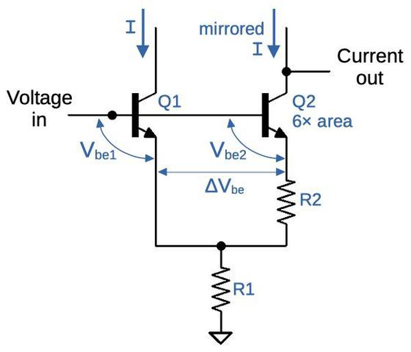
The schematic below shows how the bandgap regulator is constructed. The key factor is the voltage between a transistor's base and its emitter (Vbe), which decreases with temperature. However, ΔVbe, the difference between the two Vbe increases with temperature. With the right resistors, these two factors cancel out, yielding a stable reference voltage. The circuit compares the input voltage to this reference voltage; see the footnote8 for more details.

Schematic of the bandgap regulator. A current mirror directs the same current through both sides of the circuit.

Schematic of the bandgap regulator. A current mirror directs the same current through both sides of the circuit.

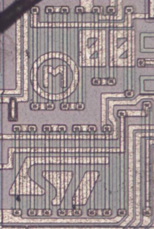
In the UVLO circuit, the bandgap reference is used to detect if the chip's input voltage falls too low. Since the input voltage is around 30 volts, a network of resistors (below) scales it to the bandgap voltage (about 1.2 volts) for comparison.9

This set of resistors forms voltage dividers to reduce the input voltage for the bandgap comparator. Note the mask date of "00" as well as the ST Microelectronics logo at the bottom.

This set of resistors forms voltage dividers to reduce the input voltage for the bandgap comparator. Note the mask date of "00" as well as the ST Microelectronics logo at the bottom.

The bandgap voltage reference

The chip uses a second bandgap reference to create an internally-regulated 5 volt supply to power the chip's circuitry. This voltage is also made available to external circuitry that may need an accurate voltage.

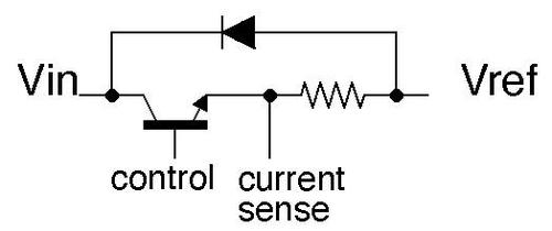
At a high level, this voltage reference is a linear power supply, with a power transistor controlling how much of the input voltage passes through to the regulated Vref. The control signal comes from the bandgap regulator, which I'll explain below. The output circuit also has a current-sense resistor to measure the output current. This limits the output current to 50 mA in case of a short circuit. A diode clamps the output if the input voltage suddenly drops.

Schematic of the Vref output circuit. The transistor limits the voltage.

Schematic of the Vref output circuit. The transistor limits the voltage.

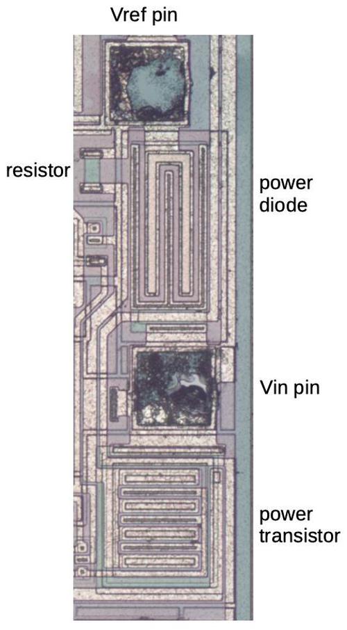
The photo below shows how this circuit is implemented on the die. The power transistor is much larger than the other transistors, so it can support a high-current output. The construction of the diode is similar to the power transistor, but without a collector. The current-sense resistor is short and wide, giving it a low resistance.

Vref output circuit on the die.

Vref output circuit on the die.

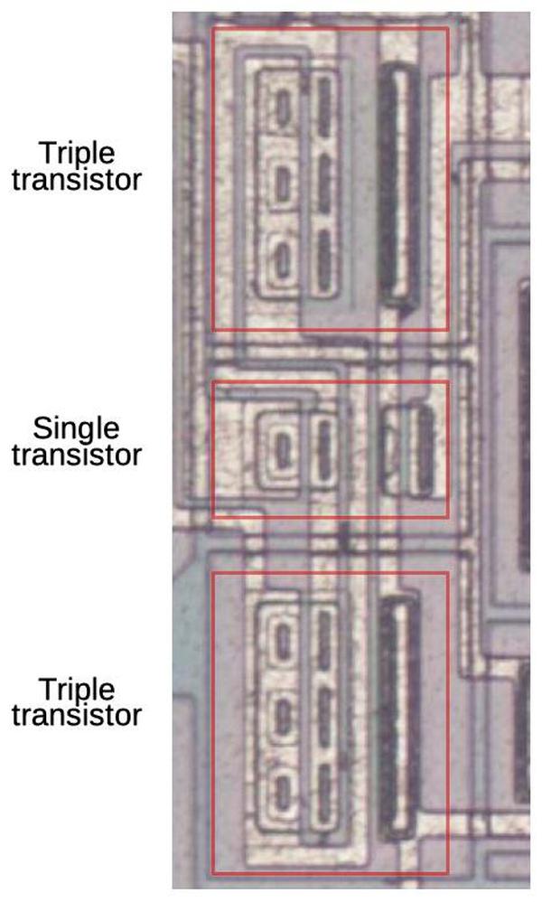
The heart of the circuit is the bandgap voltage reference below. The circuit is similar to the bandgap voltage reference for the under-voltage lockout circuit, using two transistors, one with six times the area of the other. However, the six-way transistor has been split into two and surrounds the single transistor. With this layout, even if there is a temperature gradient across the die, the single-transistor and the six-transistor will be at the same average temperature.

The transistors at the heart of the bandgap reference.

The transistors at the heart of the bandgap reference.

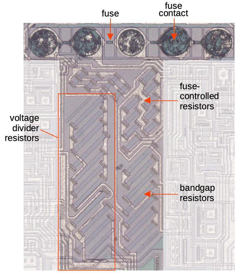
The accuracy of the bandgap regulator depends on the accuracy of its resistors. During manufacturing, fuses are blown to tune the resistance, as with the oscillator's resistors. The photo below also shows the resistors that form a voltage divider to reduce the 5-volt output to the 1.2-volt bandgap voltage. In contrast to the thin meandering resistors used elsewhere, these resistors are thick and uniform length to improve their accuracy.

Resistors that control the bandgap reference.

Resistors that control the bandgap reference.

Output

At this point, I'll step back and review the chip's function in the power supply. It controls the switching transistor, causing the transistor to send high-voltage pulses through the transformer. The chip does this by producing control pulses on its output pin. Since the switching transistor is fairly large, the chip outputs a relatively high current (200 milliamps) control signal. This requires fairly large output transistors inside the IC.

The controller chip directs the switching transistor to send pulses through the transformer.

The controller chip directs the switching transistor to send pulses through the transformer.

The die photo below shows the IC's two output transistors: the upper one pulls the output high, and the lower one pulls the output to ground. One interesting feature of the chip is that it has two pads on the die for Vin and two pads for ground. The purpose of this is that the output transistors draw a lot of current, which could cause noise fluctuations on the power and ground lines, interfering with the rest of the chip. By providing separate pads, the output transistor is somewhat isolated from the rest of the circuitry.10

Two large transistors drive the output pin.

Two large transistors drive the output pin.

Variants

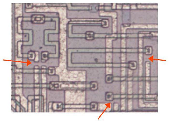
One interesting thing about this chip is that four different chips are manufactured from the same silicon. The UC3842 has a 16-volt UVLO threshold, while the UC3843 has an 8.5-volt threshold for lower-voltage applications. Other variants of the chip (UC3844 and UC3845) have a flip flop to reduce the pulse duty cycle. These different chips use slightly different metal wiring over the same silicon base. (It's easier to customize the metal layer than the silicon.) The photo below shows some places where the metal wiring has been severed in the UC3842 to change the wiring.

Closeup of the die with some broken connections indicated with arrows.

Closeup of the die with some broken connections indicated with arrows.

Conclusion

Power supplies are usually taken for granted, but they contain a lot of interesting technology. The invention of the power supply control chip in 1975 is a key step in the history of power supply improvements. Modern power supply chips are much more complex, with features to improve efficiency and reduce interference, but the chip that I examined uses the same basic principles.11 Analog chips are built from several important building blocks such as differential amplifiers, current sources, current mirrors, and bandgap voltage references. The UC3842 chip illustrates all of these building blocks, and how they are combined to build complex circuits.

I announce my latest blog posts on Twitter, so follow me at kenshirriff. I also have an RSS feed.

Notes and references

  1. For schematics of power supplies using this UC3842 chip, see this site, near the bottom of the page. 

  2. The idea of a Zener diode is that it blocks current like a normal diode until it reaches the "breakdown voltage", where it starts conducting. Zener diodes are often formed on chips from the emitter-base junction of NPN transistors, which commonly results in a 6.8-volt breakdown voltage. Looking at the photo, you can see 5 transistor-like structures in series. At 6.8 volts each, this generates the 34-volt breakdown voltage shown in the block diagram. 

  3. The oscillator's comparator is set to turn off about 1.6 volts below the level at which it turns on, that is it has hysteresis. This ensures that the capacitor discharges significantly rather than settling around the discharge level. The oscillator design is a bit like the 555 timer, with discharge and charge phases triggered by the capacitor voltage. 

  4. Many of the resistors in the fuse network are made of fixed-length resistors in various combinations. For example, two in parallel gives twice the resistance, while two in series give half the resistance. The advantage of combining fixed-length resistors is that the resistances are more predictable than making resistors of different lengths. The different resistors have roughly binary values, so different combinations of blown fuses select a variety of resistances. 

  5. I think that the chip uses Zener antifuses, since they look similar to NPN transistors without a collector. The process of blowing the antifuse to make it conductive is called a "Zener zap." 

  6. The current mirror uses a buffered-feedback design with emitter degeneration resistors (details). The small emitter resistors improve the output impedance. Three of the transistors in the current mirror are set up to split current, so each sinks one-third of the regular current. Another transistor has a larger emitter resistor, reducing the current; a small change in resistance yields a large change in the current. This illustrates the flexibility of a current mirror to produce different currents. 

  7. The block diagram shows a resistor-diode network between the error amplifier and the current sense comparator. This network scales and clips the error amplifier output to make its levels more useful. The circuitry isn't particularly interesting, so I won't discuss it in detail. I'll mention, though, that the block diagram shows the error amplifier output uses two diodes to drop its voltage. The circuit, on the other hand, raises the other signals by two diode levels instead, which works out the same mathematically. (Transistors are used to implement the diode drops as well as the 1-volt Zener.) 

  8. The details of a bandgap reference are too complex to explain here, but I'll give a brief overview in this footnote. The basis is that the voltage between a transistor's base and emitter scales drops linearly with the temperature (in Kelvin). But since the two transistors have different areas, the two transistors have different scale factors. The difference between the two transistors' base-emitter voltages increases linearly with temperature. By combining a voltage that decreases linearly with temperature and a voltage that increases linearly with temperature, you can create a voltage that remains almost constant with temperature. This voltage turns out to be the bandgap voltage of silicon, about 1.2 volts.

    Scaling and combining these voltages is done by two resistors, so it is important that temperature doesn't affect the resistances. The circuit is designed so that only the ratio between resistances matters, so if temperature affects both resistors equally, the circuit is unaffected. A problem is that a temperature gradient on the chip could affect some resistors more than others, but the chip uses a clever layout technique to avoid this. There are seven resistor segments: one forms a resistor and six are in series to form a resistor with six times the resistance. The one-unit resistor is put in the middle with three segments above and three segments below. If a temperature gradient, for instance, increases the upper resistances, the resistor in the middle will have an "average" increase, while the 6-unit resistor will have three resistor segments with a large increase and three with a small increase, which will cancel out.

    The bandgap circuit doesn't explicitly generate a 1.2-volt output. Instead, it implicitly compares the input voltage with 1.2 volts. The circuit is set up so a 1.2-volt input balances the currents through both transistors. If the voltage increases, the single transistor passes more current than the six-unit transistor. A current mirror forces each side of the circuit to have the same current, with the result that the "extra" current flows through the output. Thus, if the input voltage is high enough, the circuit produces an output current, activating the chip. But if the input voltage is too low, the circuit doesn't produce an output current, shutting down the chip.

    For more information, see the optimistically-titled How to make a bandgap voltage reference in one easy lesson

  9. Another feature of the under-voltage lockout circuit is hysteresis; it has a higher voltage to turn on than to shut off. The purpose of this is to make sure the power supply doesn't oscillate on and off if the input voltage is near the threshold. Hysteresis is implemented through the input voltage divider, which uses three resistors. If the chip is activated, a transistor feeds the supply voltage into the second resistor, increasing the divider's output voltage. The result is that once the chip is active, the supply voltage must drop more to turn the chip off. 

  10. Surprisingly, the chip has two pads for power and two pads for ground, but only single power and ground pins. Instead, two bond wires go from the pads to each external power and ground pin. Although this doesn't provide complete separation between the chip's power and the output circuit's power, it is still beneficial since the bond wires are thicker than the metal traces and have lower resistance.

    Although this IC is usually packaged in an 8-pin package, some manufacturers, such as Fairchild, make versions of the UC3842 in 14-pin packages. The extra pins allow separate pins to be used for the circuitry and output power and grounds. 

  11. While the UC3842 chip was introduced in 1984, the one I examined has a mask date of "00", so this design is from 2000. The power supply itself was from 2005. 

Inside a 20-Watt Traveling Wave Tube Amplifier from Apollo

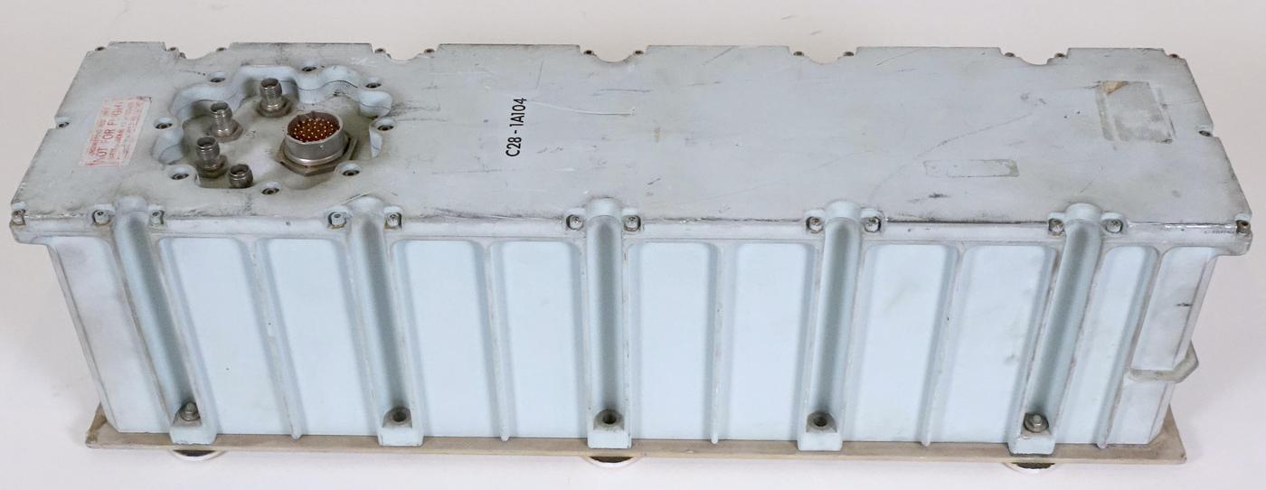
How did the Apollo astronauts communicate on their trip to the Moon, 240,000 miles back to Earth? They used a 32-pound amplifier, built around a special kind of vacuum tube called a traveling-wave tube. In this blog post, I look inside this amplifier and explain how the traveling-wave tube works.

The Collins Radio traveling-wave tube amplifier. The label says "Not for flight" so this amplifier was only used on the ground. Click this photo (or any other) for a larger version.

The Collins Radio traveling-wave tube amplifier. The label says "Not for flight" so this amplifier was only used on the ground. Click this photo (or any other) for a larger version.

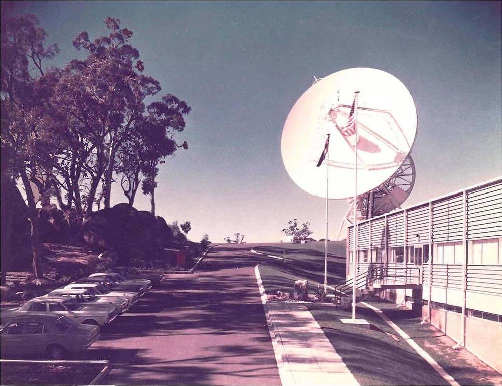
Surprisingly, this amplifier only produced 20 watts of power, not much more than a handheld walkie-talkie.1 You might wonder how a 20-watt signal could be received all the way from the Moon. To pick up the weak signal, NASA built a network of 26-meter (85-foot) dish antennas that spanned the globe, with ground stations in Spain, Australia, and California. For the signal to the spacecraft, the ground stations broadcast a strong, focused 10,000-watt signal that could be picked up by the spacecraft's small antennas. Additional ground stations with smaller 9-meter (30 foot) antennas filled in coverage gaps, along with tracking ships and airplanes.2

NASA's 26-meter antenna at Honeysuckle Creek, Australia. Photo from NASA.

NASA's 26-meter antenna at Honeysuckle Creek, Australia. Photo from NASA.

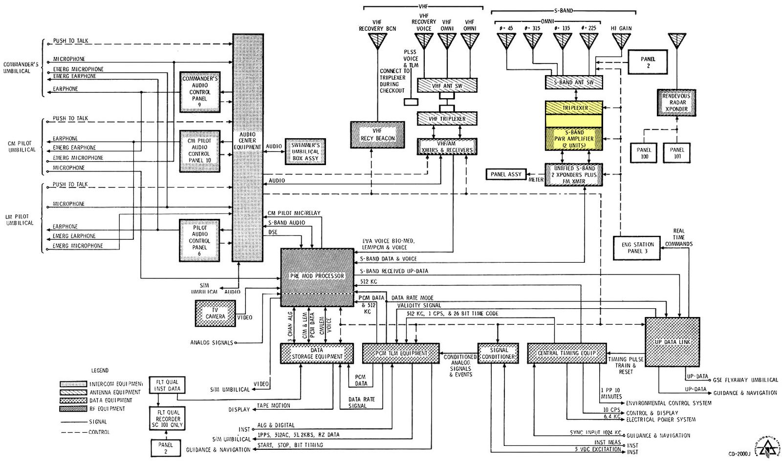
The communication system on Apollo was very complex, as shown in the diagram below. The amplifier, highlighted in yellow, was just one component of this system (which I'm not going to try to explain here). Most communication went over the "Unified S-Band", which sent voice, data, telemetry, TV, control, and ranging through one unified system. In comparison, the Gemini missions used separate systems for different purposes. (S-band refers to the microwave frequency band used by this system.)

Diagram of the Apollo Block II Telecommunications System. (Click for a larger version.) From "Apollo Logistics Training", courtesy of Spaceaholic.

Diagram of the Apollo Block II Telecommunications System. (Click for a larger version.) From "Apollo Logistics Training", courtesy of Spaceaholic.

Inside the amplifier

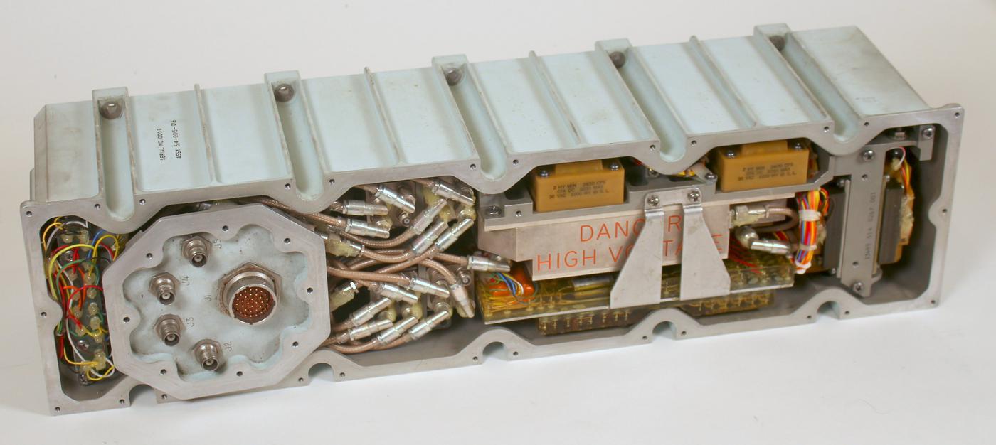
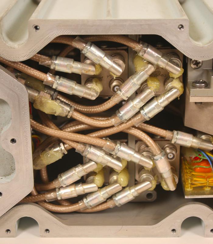
The amplifier was built by Collins Radio, a company that had a large role in the space program.3 (Collins claims that from Mercury and Gemini to Apollo, every American voice transmitted from space was via Collins Radio equipment.) The photo below shows the amplifier with the cover removed, showing the circuitry inside. Note the tangles of coaxial cables for the high-frequency RF signals. The "Danger High Voltage" warning is due to the thousands of volts required by the traveling-wave tubes.

Inside the amplifier, many coaxial cables connect the RF circuitry.

Inside the amplifier, many coaxial cables connect the RF circuitry.

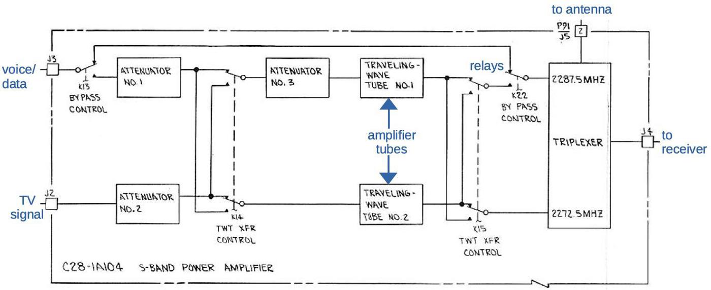
The block diagram below shows the structure of the amplifier,4 centered on the two traveling-wave tubes that perform the amplification. The amplifier takes two inputs: voice/data and the TV signal. In normal use, one tube amplifies the voice/data signal and the other amplifies the TV signal. An important feature is that either signal can be sent to either tube, or the amplifier can be bypassed entirely. This allows communication if a tube fails, or even if the amplifier entirely fails. The signals are directed by RF relays, electrically-controlled switches. The triplexer sends the two amplified signals to the antenna, and directs the signal from the antenna to the receiver.)

Simplified block diagram of the amplifier. From CSM Functional Integrated System Schematics.

Simplified block diagram of the amplifier. From CSM Functional Integrated System Schematics.

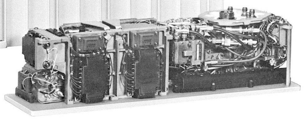
The photo below shows the amplifier with the case removed. (We were unable to disassemble the amplifier completely so this photo is from the documentation.5) The traveling-wave tube is the black cylinder at bottom right, about 10 inches long. The second tube is in the same position on the back of the amplifier.

Photo of the traveling-wave tube amplifier used in Apollo. Photo from
Collins S-Band Power Amplifier.

Photo of the traveling-wave tube amplifier used in Apollo. Photo from Collins S-Band Power Amplifier.

How a traveling-wave tube works

The traveling-wave tube (TWT) is the heart of the amplifier. TWT systems have been popular for satellites because they are compact and provide high amplification with very wide bandwidth.7 They are still widely used in satellites, radar, and other systems.

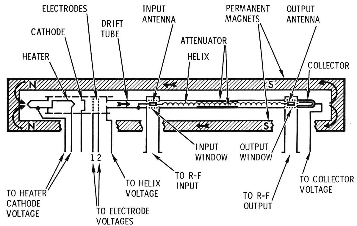
A traveling-wave tube uses an interesting technique to amplify the input RF signal, different from typical vacuum tubes. It creates a beam of electrons and transfers energy from this beam to the RF signal. In more detail, an electron gun shoots electrons down the tube, (a bit like a CRT). As these electrons travel through the tube, they interact with the RF signal and bunch together, transferring energy to the RF signal.6

The problem is that the electron beam and the RF signal need to travel at approximately the same speed in order to interact, but the electron beam travels at about 10% the speed of light,8 while the RF signal travels at the speed of light. The trick is to put the RF signal through a helix, wrapped around the beam. Because the RF signal travels through the long helix rather than in a straight line, its path through the tube is slowed. With the proper helix design, the RF signal and the electron beam travel at approximately the same net speed down the tube, allowing them to interact.

Diagram of the TWT amplifier. From "Apollo Logistics Training", courtesy of Spaceaholic.

Diagram of the TWT amplifier. From "Apollo Logistics Training", courtesy of Spaceaholic.

The diagram above shows the components of the traveling wave tube in detail. The heart of the TWT is the drift tube that holds the electron beam, wrapped in the helix for the RF signal. At the left, the electron beam is created by the components of the electron gun (heater, cathode, and electrodes). The RF input and output provide the connections to the helix for the signal that is being amplified. The collector absorbs the weakened electron beam after it has passed through the tube. Finally, the permanent magnets keep the electron beam focused through the tube.

It's hard to see the traveling-wave tube inside the amplifier, since it is mounted at the bottom under a bunch of coaxial cables; the photo below is the best I could do. The tube looks like a black cylinder, but you can see the coaxial cables attached at the left and right.

The traveling-wave tube inside the amplifier.

The traveling-wave tube inside the amplifier.

Other parts of the amplifier

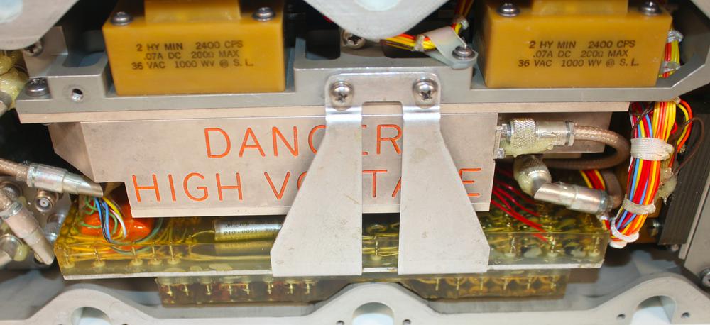
Next, I'll briefly describe the other circuitry inside the amplifier. A traveling wave tube requires high voltage to accelerate the electron beam. The photo below shows two of the power supply transformers. The amplifier was powered with 115 volts AC, 3-phase at 400 cycles per second. It also used 28 volts DC for the control circuitry. Note the circuitry encased in plastic at the bottom of the photo.

The amplifier uses high-voltage transformers to power the traveling-wave tubes.

The amplifier uses high-voltage transformers to power the traveling-wave tubes.

As described earlier, the RF relays switch signals between the two tubes to provide redundancy. The relays (below) are the fairly large square units with coaxial cables attached. These relays are more complex than typical relays because they must transfer gigahertz RF signals. The internal wiring is constructed from metal strips between double ground planes along with waveguides.

The relays with coaxial cables attached.

The relays with coaxial cables attached.

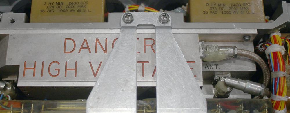
Another interesting component of the amplifier is the triplexer, a special RF component that connects the antenna to the amplifier. The idea of the triplexer is that it has three ports, each for a different frequency, and keeps the signals on each port separate from each other. Specifically, it combines the main 2287.5 megahertz signal with the TV's 2272.5 megahertz signal and sends these to the antenna. The signal from the ground is at 2106.4 megahertz; the triplexer directs this signal from the antenna to the receiver. Internally, the triplexer has band-pass filters for each frequency, providing a large amount of isolation (60 dB) between its three ports.

The triplexer.

The triplexer.

The triplexer is the metal box in the photo above. Note the coax connections with the antenna connection labeled. Although the triplexer says "Danger High Voltage" on top, this refers to the surrounding power supply circuitry, not the triplexer itself.

Controlling the amplifier

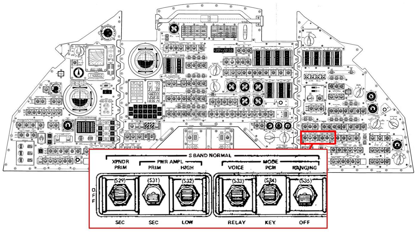
The astronauts had control switches in the Command Module to turn the power amplifier on and off, and switch between the primary and secondary tubes. The diagram below shows the location of these switches, marked PWR AMPL. The PRIM/SEC selects which tube was used for the main signal and which was used for the TV signal. The HIGH/OFF/LOW switch selected the power output level for the amplifier. When the amplifier was off, the input signal was connected directly to the antenna, bypassing the amplifier.

Astronauts controlled the amplifier through switches on the console. Diagram from Command/Service Module Systems Handbook p208.

Astronauts controlled the amplifier through switches on the console. Diagram from Command/Service Module Systems Handbook p208.

Conclusion

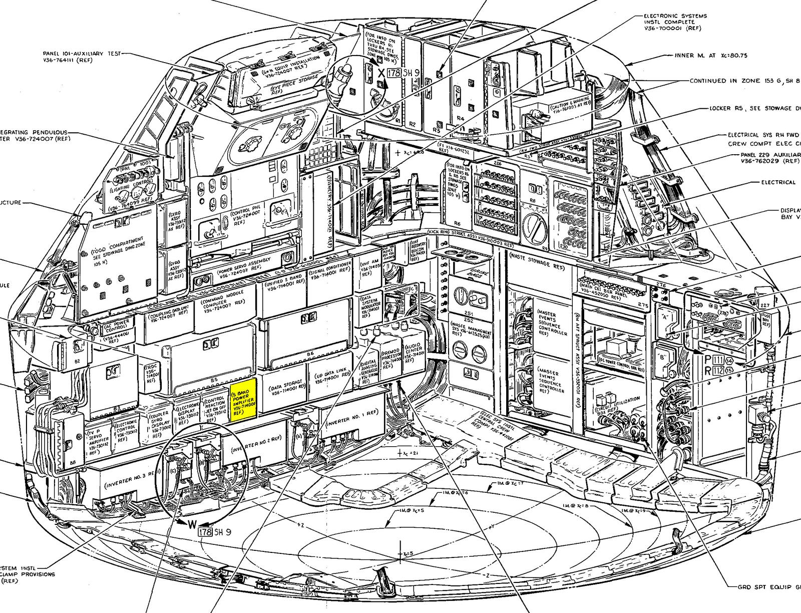
This power amplifier illustrates the complexity of the communication systems for Apollo.9 Even though the amplifier is complex internally with redundant traveling-wave tubes, it is just one of many pieces of hardware. The diagram below shows the Command Module's equipment bay, with the amplifier highlighted in yellow. (The Apollo Guidance Computer was directly above the amplifier, two rows up.)

Diagram of the Apollo Command Module's equipment bay with the S-band power amplifier highlighted.
From Command/Service Module Systems Handbook p212.

Diagram of the Apollo Command Module's equipment bay with the S-band power amplifier highlighted. From Command/Service Module Systems Handbook p212.

We are currently investigating the possibility of powering up this amplifier to see if it still operates. I announce my latest blog posts on Twitter, so follow me @kenshirriff for updates. I also have an RSS feed. Thanks to Steve Jurvetson for loaning me this amplifier. Thanks to Spaceaholic and Mike Stewart for providing diagrams and the Collins Aerospace Museum for additional information.

Notes and references

  1. Walkie-talkies typically use 0.5 to 5 watts of power, with some models providing 8 watts, mostly limited by FCC regulations. There are a few 20-watt or even 25-watt handheld radios. 

  2. This photo shows the Vanguard tracking ship. This ship was a surplus tanker from World War II that was repurposed as a missile tracking ship by covering it with antennas. NASA used the ship for communication with Apollo, and the ship was scrapped in 2013.

    The Vanguard ship, from Wikimedia.

    The Vanguard ship, from Wikimedia.


  3. The document Collins S-Band Power Amplifier has technical specifications for the amplifier. The presentation Collins Role in Space Communications describes the Collins equipment used in Mercury, Gemini, and Apollo. Collins built equipment for the spacecraft and transmitting and receiving equipment on the ground. 

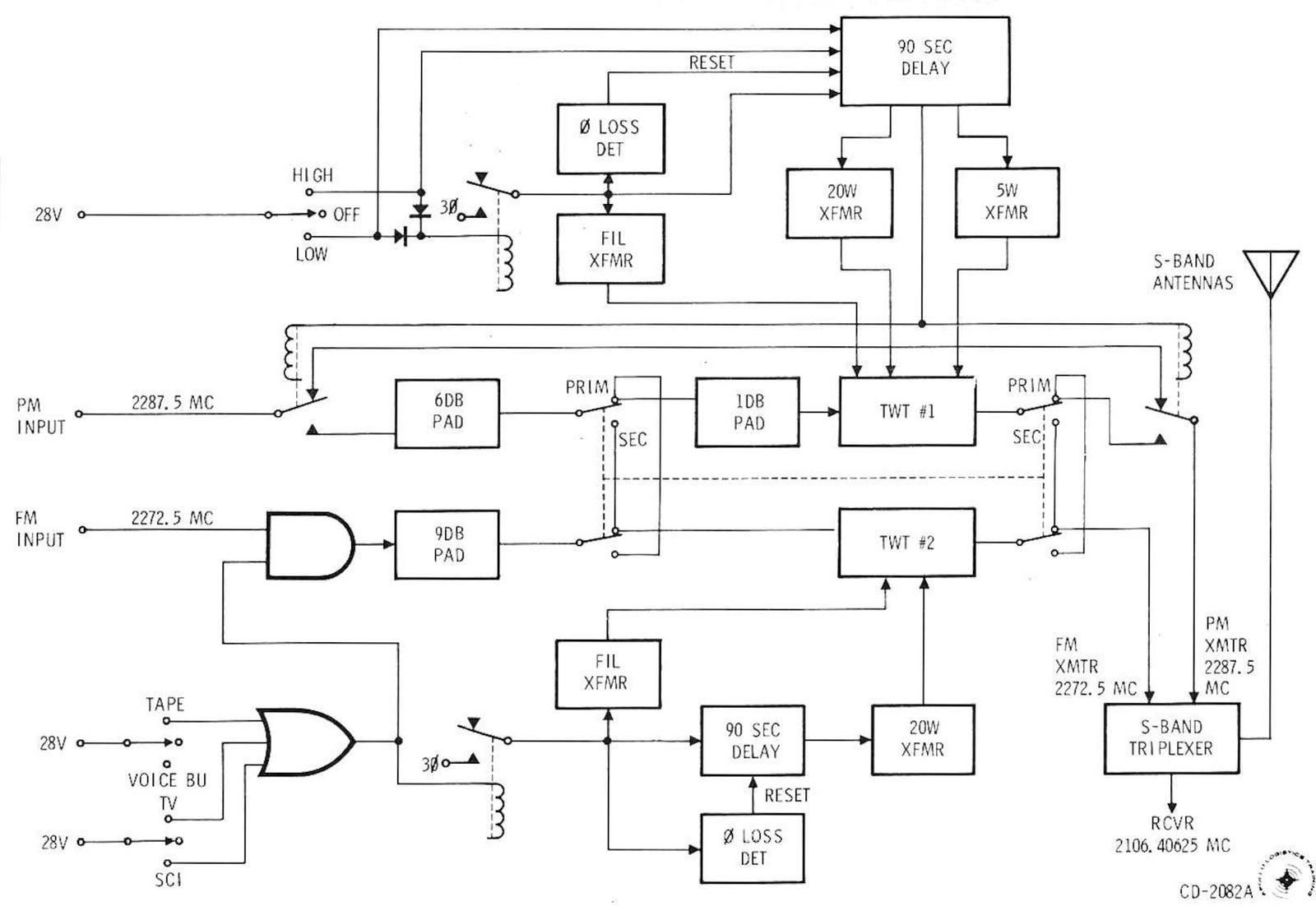
  4. Here's a more detailed diagram of the power amplifier circuitry. This diagram shows the power supply and control circuitry in more detail. In particular, the circuitry lets the tubes heat up for 90 seconds before use. Circuitry also shuts down the power if there is a fault or loss of a power phase.

    The power amplifier diagram.  From "Apollo Logistics Training", courtesy of Spaceaholic.

    The power amplifier diagram. From "Apollo Logistics Training", courtesy of Spaceaholic.


  5. The Collins photo makes it look like you can simply remove the case from the amplifier. However, the photo is misleading since the amplifier doesn't come apart like that. We attempted to remove the amplifier from the case, but it is fastened with many inaccessible screws and some components are glued down. We suspect that the amplifier was assembled inside the case, making it very difficult to perform any pre-launch maintenance. We gave up on disassembling the amplifier completely, which is why all our photos show the view from the top. 

  6. The interaction between the electron beam and the RF signal in the helix is complex, but the net result is that energy is transferred from the beam to the signal. Specifically, the electric field from the RF signal produces positive and negative waves. These accelerate and decelerate the electrons, causing them to bunch together. (On the whole, the electron beam decelerates more than it accelerates, so it loses energy.) The moving bunches of electrons induce more current in the helix, strengthening the RF signal. The result is a feedback loop, causing the RF signal to grow exponentially as it travels through the tube.

    For more information on how traveling-wave tubes work, see Traveling Wave Tube, Recent theory of traveling-wave tubes, or this long presentation

  7. A traveling-wave tube can amplify a large range of frequencies (i.e. it has a high bandwidth) because it doesn't have any resonant elements (unlike a klystron, for instance). Thus, it doesn't need to be tuned to a particular frequency. 

  8. Ignoring relativistic effects, the speed of an electron beam accelerated by a voltage is given by

    Equation for electron beam speed.

    Equation for electron beam speed.

    where v0 is the velocity, Vb is the voltage, e is the charge of an electron, and me is the mass of an electron. For example, applying 6000 volts yields an electron speed of 46,000 km/second, about 15% the speed of light.

    This equation is a rearrangement of the kinetic energy from the velocity and the energy from the voltage potential difference.

    Kinetic energy equation.

    Kinetic energy equation.

    In the traveling-wave tube, the electron beam must be slightly faster than the (net) RF signal speed so the beam will transfer energy to the RF signal as the beam is slowed.


  9. For more information on Apollo communication, see Apollo Experience Report - S-Band System Signal Design and Analysis. See also CSM Functional Integrated System Schematics and Command/Service Module Systems Handbook

"Space age electronics": Inside a GE thin-film paperweight from the 1960s

In the early 1960s, General Electric developed a technology called thin-film electronics.1 These circuits were built from thin films of material, much more compact than individual components. For weight-sensitive applications such as satellites and military equipment, thin-film electronics could potentially be revolutionary.

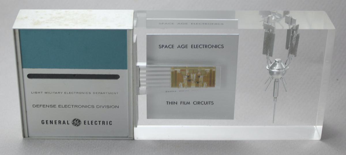
The GE paperweight consists of circuitry and a satellite model encased in thick clear plastic. It is labeled "Light Military Electronics Department, Defense Electronics Division, General Electric. Space Age Electronics, thin film circuits."

The GE paperweight consists of circuitry and a satellite model encased in thick clear plastic. It is labeled "Light Military Electronics Department, Defense Electronics Division, General Electric. Space Age Electronics, thin film circuits."

GE's Light Military Electronics department1 built the paperweight above to showcase their "Space Age Electronics". In the center is a thin-film circuit, next to a model of an early satellite. However, the paperweight contained a surprise: when picked up, the paperweight emitted a beep-beep-beep noise, sounding just like a satellite.2 In this blog post, I reverse-engineer the "Space Age Electronics" inside this paperweight and explain how it works. In brief, the visible thin-film circuit implements a flip flop. The remaining circuitry is hidden in the compartment on the left: two oscillators that produce the beeps. These oscillators are implemented in another unusual 1960s technique called "cordwood'.

The thin-film module

The most visible part of the paperweight is the thin-film module. The idea behind thin film is to build resistors and capacitors as thin layers on a substrate, rather than using individual components. Resistors are formed from thin strips of resistive material, the vertical reddish-brown lines on the module's surface. For higher resistance, these lines zig-zag back and forth.3 Capacitors are formed from two thin layers of metal (the plates), separated by an insulating dielectric material.

This angle view shows how the semiconductor components are mounted above the thin film circuitry.

This angle view shows how the semiconductor components are mounted above the thin film circuitry.

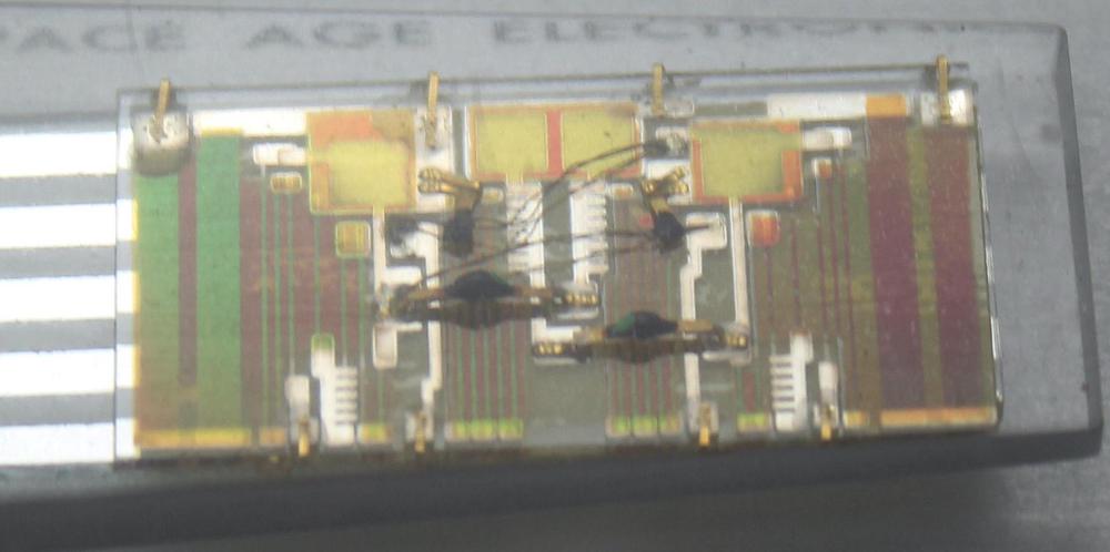
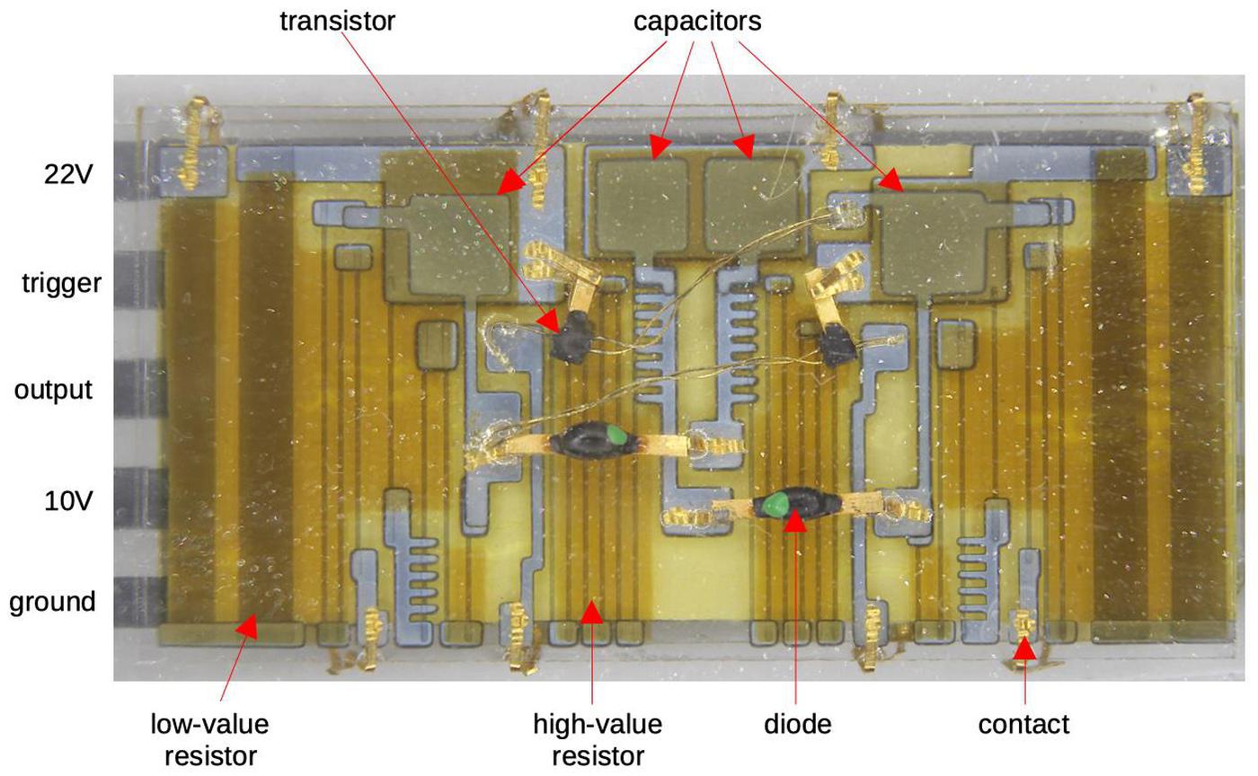
Thin-film transistors were not commercially practical in the 1960s, so the module has tiny discrete transistors and diodes mounted on top, connected by golden wires. (This must have been expensive to manufacture.) In the photo above, the shadows show that the semiconductor components (black blobs) are slightly above the surface. You can distinguish the diodes by their green dots. At the left, five metallic strips provide power and signal connections to the module, with golden contacts connecting these strips to the thin-film circuitry.

A closeup of the thin-film module.

A closeup of the thin-film module.

Interest in thin-film technology declined in the mid-1960s as integrated circuits became commercially available. Integrated circuits were cheaper, could fit more components into a chip, and could be mass-produced. For these reasons, integrated circuits took over the electronics market. Thin-film circuits are still used, but only for specialized applications.

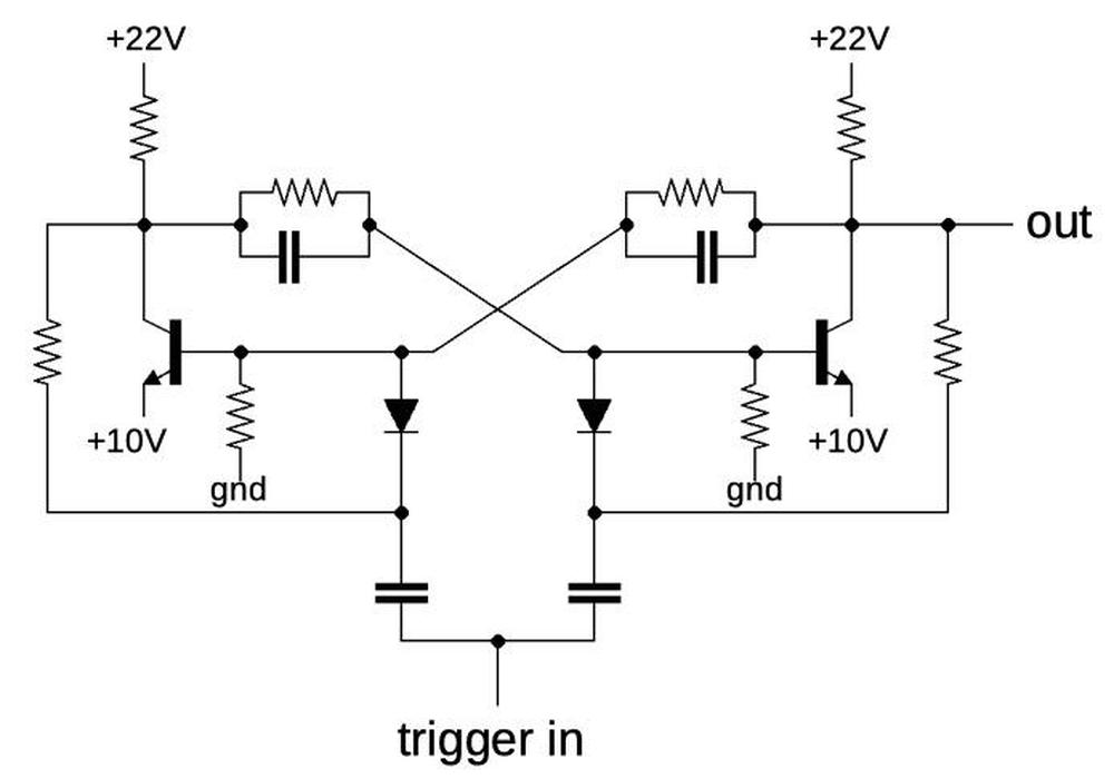
I traced out the paperweight's thin-film circuit and found that it implements a toggle flip flop, a standard electronic circuit. The flip flop stores either a 1 state or a 0 state, like a single bit of memory. When it gets a negative pulse on the trigger input, it flips to the opposite state. Thus, as it receives input pulses, it goes "on", "off", "on", "off", etc. In the paperweight, the flip flop creates the separate beeps. The paperweight generates a beep while the flip flop is on, and is silent when the flip flop is off.

Schematic of the circuit in the thin-film module.

Schematic of the circuit in the thin-film module.

You can match up the components in the schematic with the components in the photo: two transistors, two diodes, four capacitors, and multiple resistors. Note that the two sides of the circuit are symmetrical, both in the schematic and in the photo. One side of the circuit is on and one side is off. Depending on which side is on, the circuit holds a 0 or a 1. See the footnote4 for more details.

Inside the paperweight

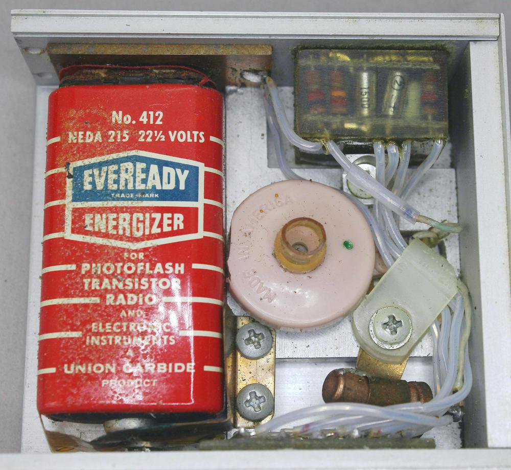
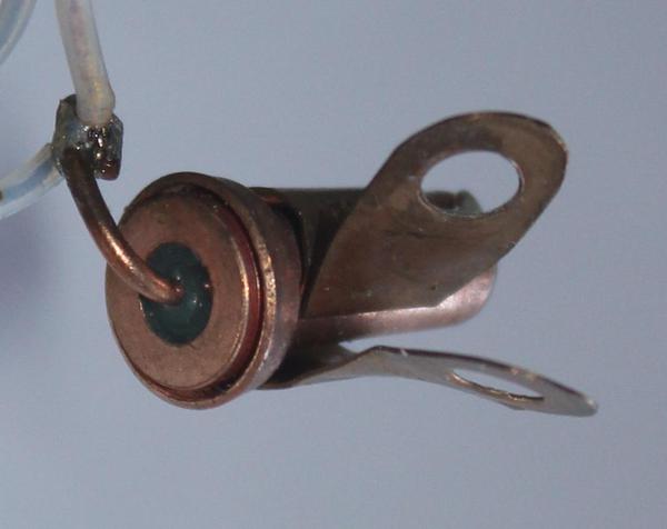
The left side of the paperweight has a compartment with some interesting circuitry inside. The paperweight was powered by a 22½ V battery, which was relatively common back then but is now obsolete. It looks a bit like a 9-volt battery, except it has one contact at each end. Next to the battery is a vintage earphone, the round pink component. It acts as the speaker in this device.

Looking inside the paperweight's compartment reveals more circuitry.

Looking inside the paperweight's compartment reveals more circuitry.

Another unusual component is the tilt switch in the lower right, which turns the paperweight on and off. (I don't know if this tilt switch contains mercury or has a rolling ball inside.) When the paperweight is horizontal, the tilt switch is open. But if the paperweight is picked up, the tilt switch closes. This probably added to the "drama" of the paperweight, since someone will think it is just a decoration until they pick it up and it starts beeping.

The tilt switch turns the paperweight on and off.

The tilt switch turns the paperweight on and off.

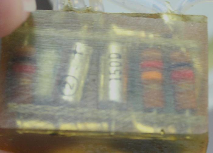
In the upper right of the compartment, a block of plastic encases the oscillator circuitry. The module is built with "cordwood" construction, a way of building high-density circuits that was popular in the 1960s. Instead of mounting components flat on a circuit board, cordwood puts components between two boards. (They are stacked together like logs, giving cordwood its name.) The photo below shows the components; it isn't as clear as I'd like because the components are embedded in yellowing plastic.

This view of the module shows three resistors (striped) and two capacitors (silver).

This view of the module shows three resistors (striped) and two capacitors (silver).

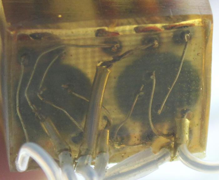
On each side of the module, components are wired with point-to-point wiring, as shown below. This photo also shows how the insulated connection wires are also embedded in the module. The large dark circles are the two transistors.

Closeup of the cordwood module, showing the wiring. The transistors and the ends of the resistors and capacitors are visible.

Closeup of the cordwood module, showing the wiring. The transistors and the ends of the resistors and capacitors are visible.

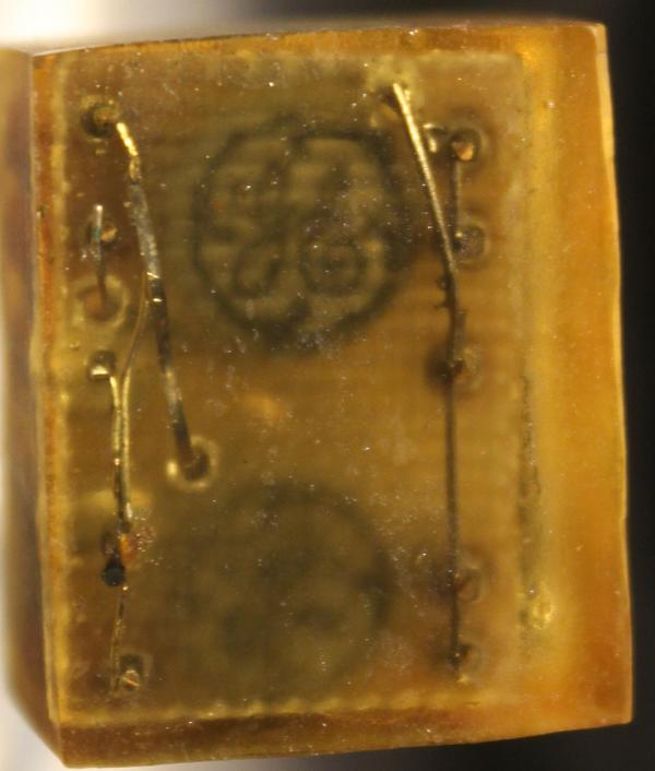
The oscillators use unijunction transistors, a somewhat unusual type of transistor, different from standard NPN and PNP transistors. Oscillators could be easily created from unijunction transistors due to their nonlinear characteristics. The unijunction transistor was invented by General Electric in 1953, so it's not surprising that General Electric made use of them in this paperweight. The GE logo is visible on top of the transistors.

In this view of the module, the script "GE" logo is visible on top of the transistors. These transistors are part number 2N491

In this view of the module, the script "GE" logo is visible on top of the transistors. These transistors are part number 2N491

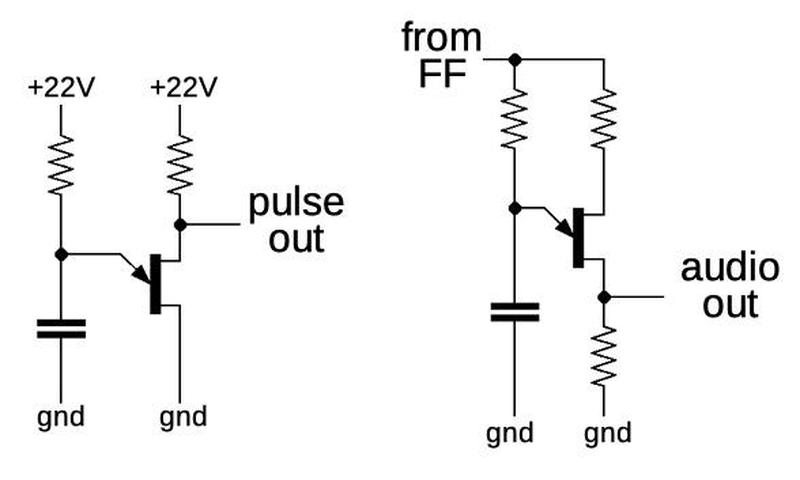
The cordwood block holds two oscillators, to control the duration of each beep and to generate the beep sound itself. The first oscillator generates five pulses per second. These pulses go to the thin-film flip-flop circuit, which will change its state between off and on with each pulse. That is, the flip flop is off for 200 milliseconds, on for 200 milliseconds, and so forth. The output from the flip flop powers the second transistor oscillator, which generates a 3.5-kilohertz tone. The result is the repeating beep-beep-beep output from the paperweight.

Schematic of the unijunction transistor oscillators.

Schematic of the unijunction transistor oscillators.

The schematic above shows the two oscillators. The idea behind a unijunction transistor oscillator is that the capacitor slowly charges through the resistor. As the capacitor charges, the voltage on the emitter (symbolized by the arrow) increases. When it reaches the trigger voltage, the transistor turns on and the capacitor discharges to ground. The cycle repeats, generating a sequence of pulses on the output.

Conclusion

I think the paperweight is from approximately 1962, based on GE's thin-film research at the time and the appearance of the paperweight's model satellite.6 The paperweight was produced in the midst of the space race; John Glenn became the first American in orbit in 1962. Satellites were still a new "space-age" thing at the time, so the paperweight was a symbol of General Electric's advanced technology.5 The beeps from the paperweight are similar to those produced by Sputnik (1957). At the time, the paperweight must have been an impressive object, a vision of the future.

Thanks to Peter B. Newman, technology collector and educator for sending me the paperweight for analysis. Thanks to Mikes Electric Stuff for identifying the tilt switch for me.

I announce my latest blog posts on Twitter, so follow me @kenshirriff. I also have an RSS feed.

Notes and references

  1. The paperweight was built by GE's Light Military Electronics department. In the early 1960s, this department produced aerospace electronics such as digital guidance computers, flight-control systems, and satellite sensors. These were used in weapons including the F-105 fighter-bomber, Sidewinder missile, and Polaris and Atlas ICBMs. 

  2. Sputnik's beeps were approximately 150-300 ms long at 1.5 kilohertz. (The frequency isn't well-defined because the transmission was just a carrier switched on and off, but this is the frequency in typical recordings.) The paperweight's beeps were approximately 200 ms long at 3.47 kilohertz. The point is that the paperweight's beeps were designed to resemble the beeps from a satellite such as Sputnik, and people would have recognized this at the time. You can hear the beeps of the paperweight here; I had to edit the audio a bit because I discovered too late that the doorbell rang in the middle of the recording. 

  3. In the module, some of the resistors are connected to the metal layer through structures that have teeth kind of like a comb. I'm not sure what the purpose of these structures is. My hypothesis is that by changing the number of "teeth", the active length of the resistor can be changed, adjusting the resistor. (Modifying the metal layer is easier than modifying the thin-film layers.) 

  4. The two transistors are cross-connected, so when one transistor is on, it forces the other one off. The trigger capacitors are pre-charged through the corresponding output. The result is that the transistor that is currently on (output low) will be pulled lower than the transistor that is currently off (output high). This turns off the first transistor, flipping the state of the circuit. It's a fairly standard flip-flop circuit; more details are here

  5. In 1960, GE hoped to build a commercial communications satellite network, and formed a subsidiary "Communication Satellites Inc" in 1960. However, GE abandoned that goal in 1961 (probably due to antitrust issues) to focus on manufacturing equipment for space vehicles. 

  6. The satellite in the paperweight resembles the Ariel 1 (1962) and Ariel 2 (1964) satellites, with its paddle-like solar cells. It's not an exact match, so I don't know if the satellite is an artist's conception, or is a different satellite. If you recognize the satellite, please let me know.