Inside the HP Nanoprocessor: a high-speed processor that can't even add

The Nanoprocessor is a mostly-forgotten processor developed by Hewlett-Packard in 19741 as a microcontroller2 for their products. Strangely, this processor couldn't even add or subtract,3 probably why it was called a nanoprocessor and not a microprocessor. Despite this limitation, the Nanoprocessor powered numerous Hewlett-Packard devices ranging from interface boards and voltmeters to spectrum analyzers and data capture terminals.4 The Nanoprocessor's key feature was its low cost and high speed: Compared against the contemporary Motorola 6800,7 the Nanoprocessor cost $15 instead of $360 and was an order of magnitude faster for control tasks.

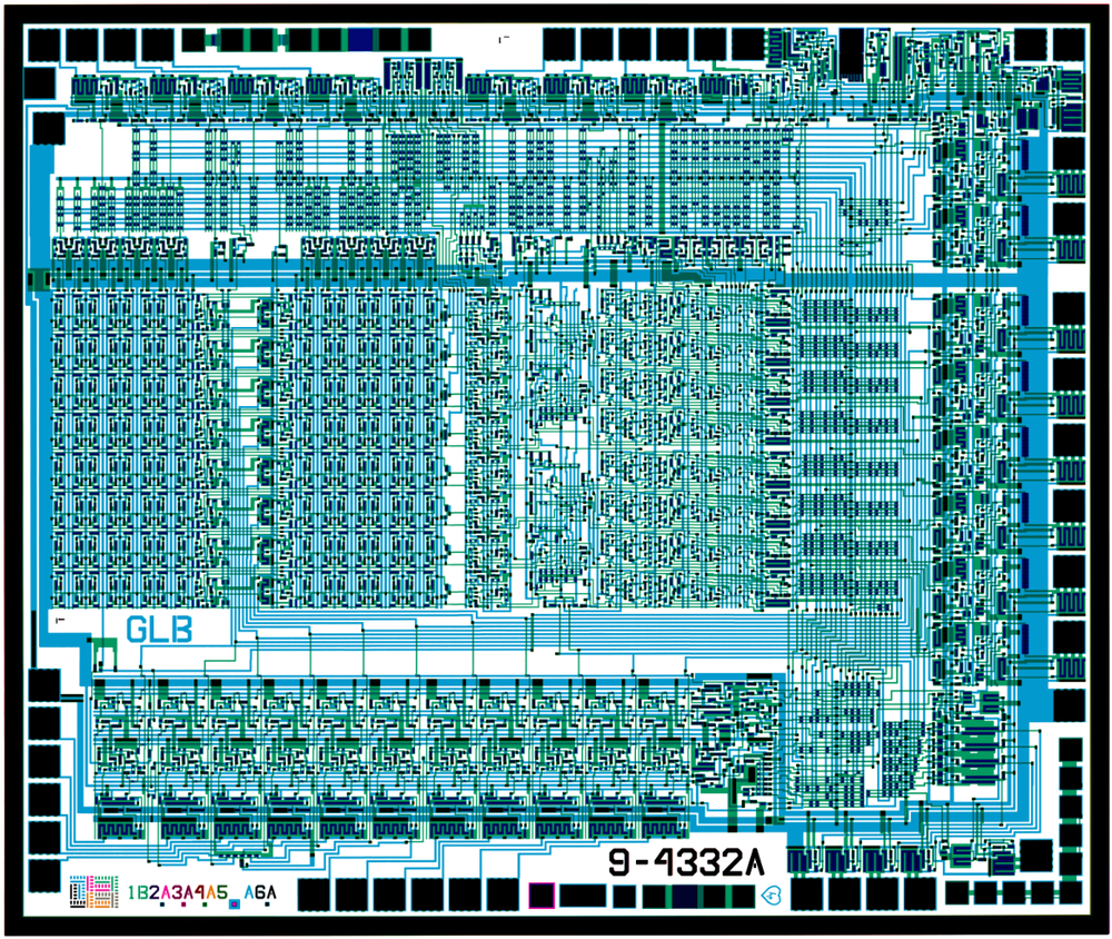
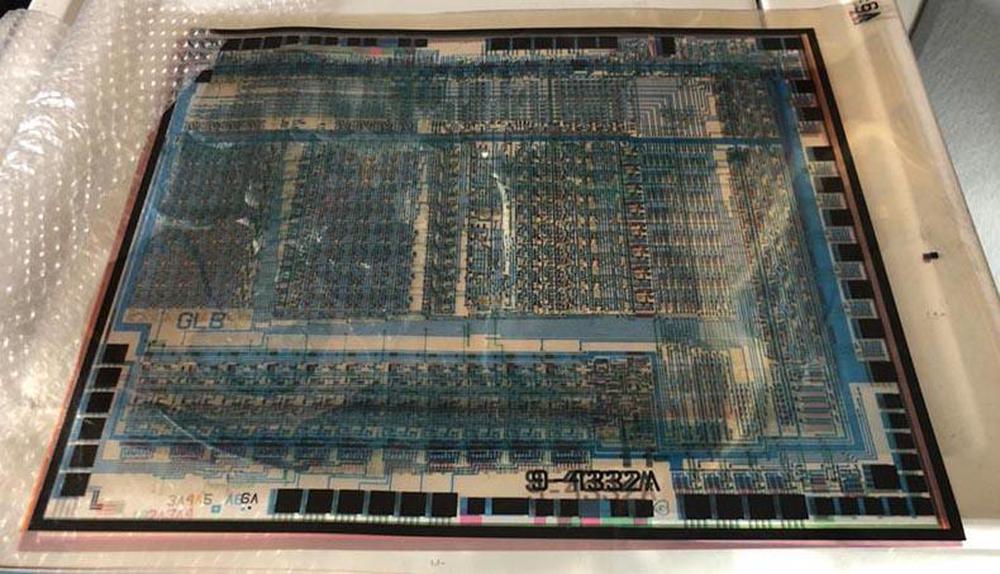
Recently, the six masks used to manufacture the Nanoprocessor were released by Larry Bower, the chip's designer, revealing details about its design. The masks were carefully cleaned and scanned by The CPU Shack, and stitched by Antoine Bercovici. The composite mask image below shows the internal circuitry of the integrated circuit.5 The blue layer shows the metal on top of the chip, while the green shows the silicon underneath. The black squares around the outside are the 40 pads for connection to the IC's external pins. I used these masks to reverse-engineer the circuitry of the processor and understand its simple but clever RISC-like design.6

Combined masks from the Nanoprocessor. Click for larger image. "GLB", to the left of the data bus, stands for the designers George Latham and Larry Bower. Files courtesy of Antoine Bercovici.

Combined masks from the Nanoprocessor. Click for larger image. "GLB", to the left of the data bus, stands for the designers George Latham and Larry Bower. Files courtesy of Antoine Bercovici from scans by The CPU Shack.

The Nanoprocessor was designed in 1974, the same year that the classic Intel 8080 and Motorola 6800 microprocessors were announced. However, the Nanoprocessor's silicon fabrication technology was a few years behind, using metal-gate transistors rather than silicon-gate transistors that were developed in the late 1960s. This may seem like an obscure difference, but silicon gate technology was much better in several ways. First, silicon-gate transistors were smaller, faster, and more reliable. Second, silicon-gate chips had a layer of polysilicon wiring in addition to the metal wiring; this made chip layouts about twice as dense.8 Third, metal-gate circuitry required an additional +12 V power supply. The Intel 4004 processor used silicon gates in 1971, so I'm surprised that HP was still using metal gates in 1974.9

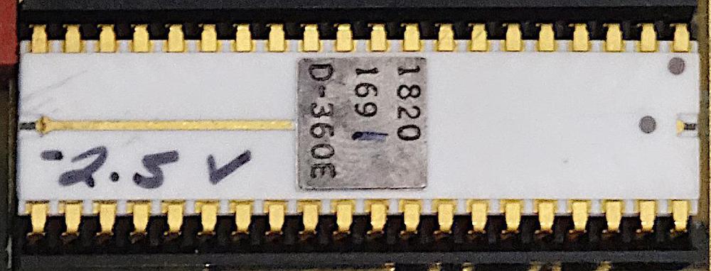
A bizarre characteristic of the Nanoprocessor is its variable substrate bias voltage. For performance reasons, many 1970s microprocessors applied a negative voltage to the silicon substrate, with -5V provided through a bias pin.10 The Nanoprocessor has a bias pin, but strangely the bias voltage varied from chip to chip, from -2 volts to -5 volts. During manufacturing, the required voltage was hand-written on the chip (below). Each Nanoprocessor had to be installed with a matching resistor to provide the right voltage. If a Nanoprocessor was replaced on a board, the resistor had to be replaced as well. The variable bias voltage seems like a flaw in the manufacturing process; I can't imagine Intel making a processor like that.

The HP Nanoprocessor, part number 1820-1691. Note the hand-written voltage "-2.5 V". The last digit (1) of the part number is also hand-written, indicating
the speed of the chip. Photo courtesy of Marc Verdiell.

The HP Nanoprocessor, part number 1820-1691. Note the hand-written voltage "-2.5 V". The last digit (1) of the part number is also hand-written, indicating the speed of the chip. Photo courtesy of Marc Verdiell.

Like most processors of that era, the Nanoprocessor was an 8-bit processor. However, it didn't use RAM, but ran code from an external 2-kilobyte ROM. It contained 16 8-bit registers, more than most processors and enough to make up for the lack of RAM in many applications. Based on transistor count, the Nanoprocessor is more complex than the Intel 8008 (1972) and slightly less complex than the 6800 (1974) or 6502 (1975).11 Its architecture uses its transistor count on different purposes from these processors, though. The Nanoprocessor lacks ALU functionality but in exchange, it has a large register set, taking up much of the die area. The Nanoprocessor has 48 instructions, a considerably smaller instruction set than the 6800's 72 instructions. However, the Nanoprocessor includes convenient bit set, clear, and test operations, which these other processors lacked.12 The Nanoprocessor supports indexed register access, but lacks the complex addressing modes of the other processors.

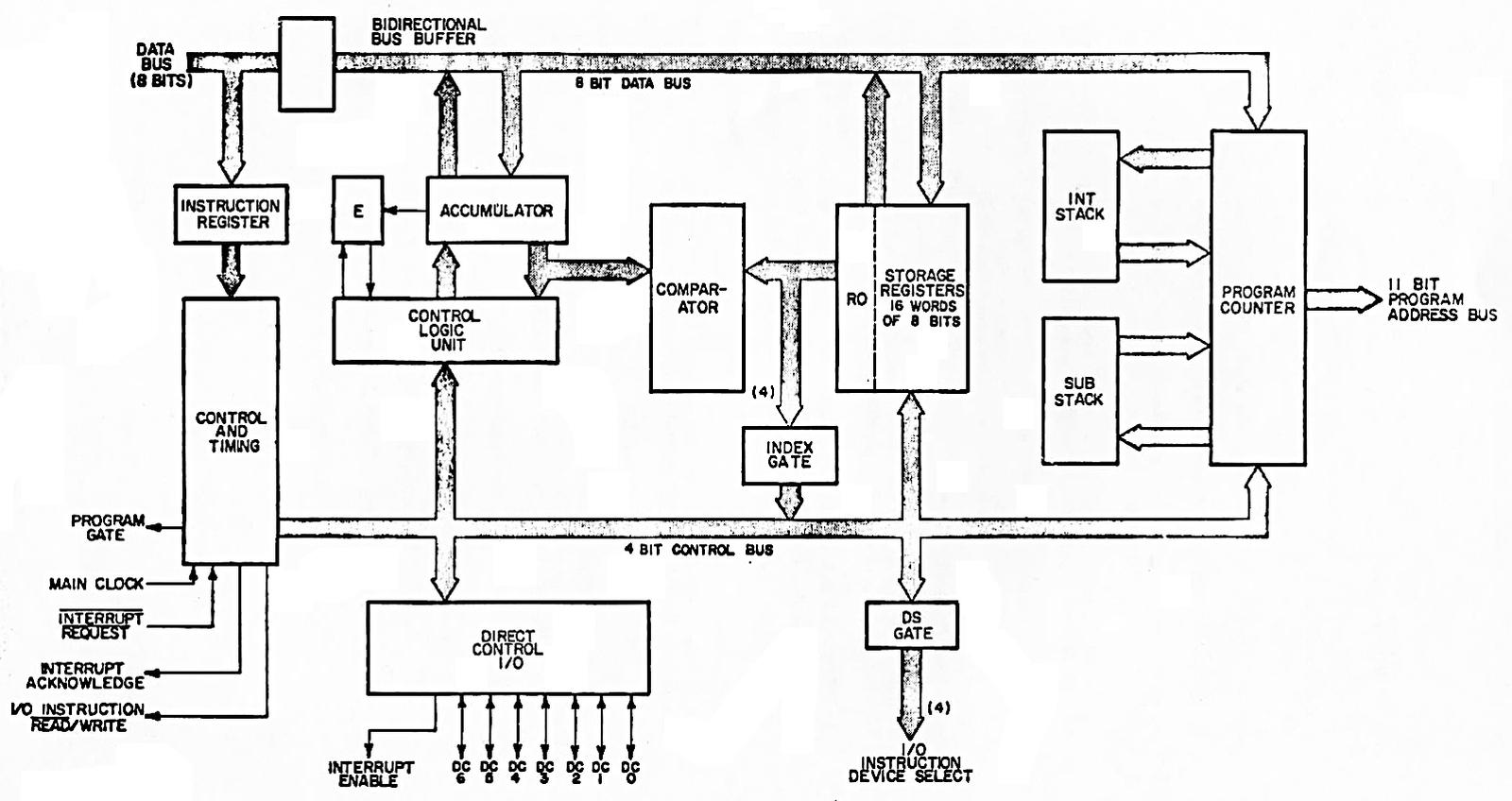
The block diagram below shows the internal structure of the Nanoprocessor. The main I/O feature is the 4-bit "I/O Instruction Device Select" which allows 15 devices to receive I/O operations. In other words, the select pins indicate which I/O device is being read or written over the data lines. External circuitry uses these signals to do whatever is necessary for the particular application, such as storing the data in a latch, sending it to another system, or reading values. More I/O is provided through seven "Direct Control I/O" pins (GPIO pins) that can be used for inputs or outputs. If not connected to external circuitry, these pins operate as convenient bit flags; the Nanocomputer can set a value and then read it back. The Control Logic Unit performs increments, decrements, shifts, and bit operations on the accumulator, lacking the arithmetic and logical operations of a standard Arithmetic/Logic Unit (ALU).

Block diagram, from the Nanoprocessor User's Guide.

Block diagram, from the Nanoprocessor User's Guide.

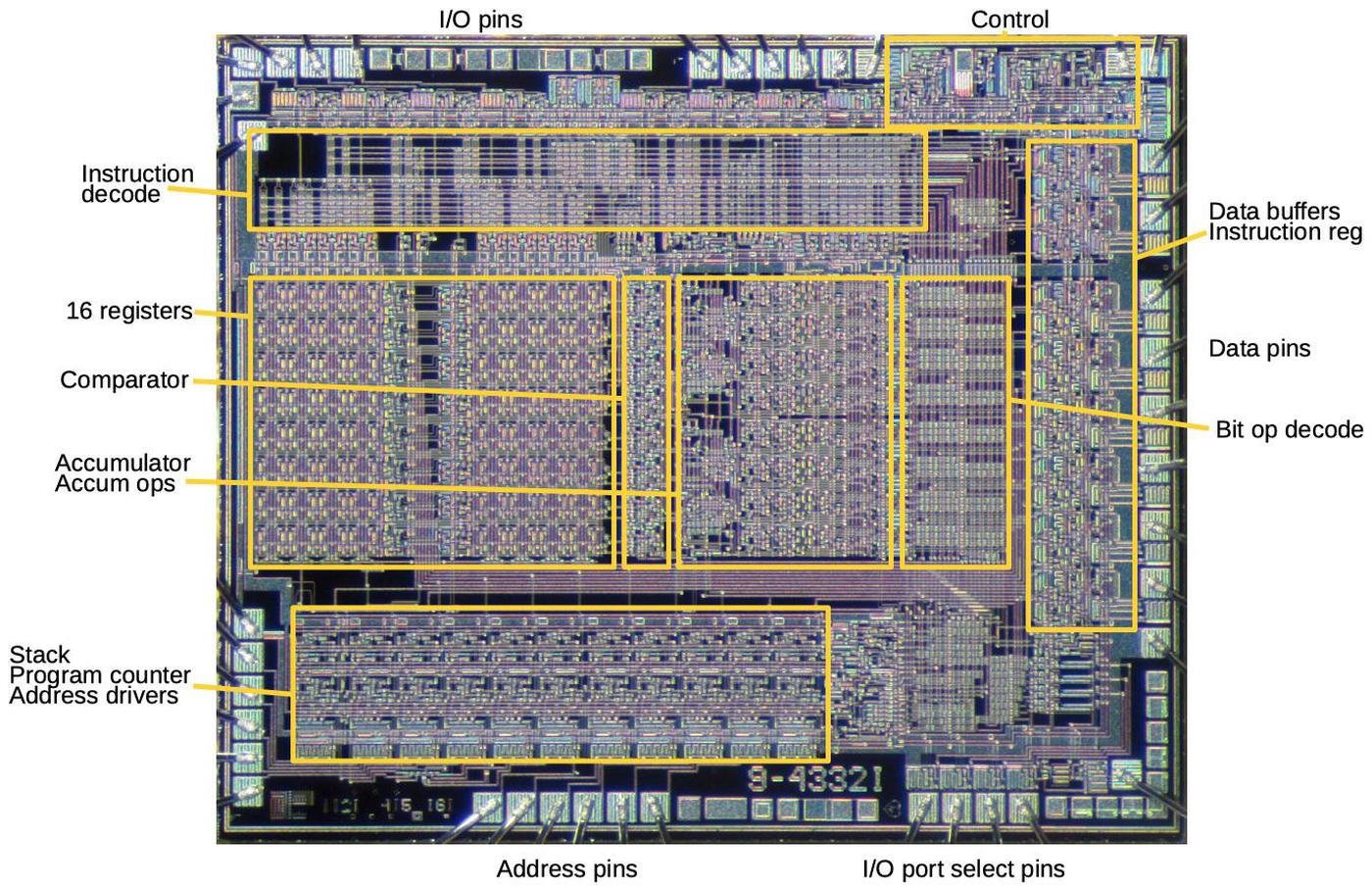
I reverse-engineered the Nanoprocessor's circuitry from the masks and determined how the functional blocks map onto the die, below. The largest feature is the set of 16 registers in the center-left. To the right is the comparator and then the accumulator, along with its increment, decrement, shift, and complement circuitry. The instruction decoder circuitry takes up much of the space above and to the right of the comparator and accumulator. The bottom part of the chip is dominated by the 11-bit program counter, along with the one-entry interrupt stack and subroutine stack. The control circuitry implements the Nanoprocessor's almost-trivial instruction timing: one fetch cycle followed by one execute cycle.13 In most microprocessors, the control circuitry takes up a large fraction of the chip, but the Nanoprocessor's control circuitry is just a small block.

Functional components of the HP Nanoprocessor, based on my reverse-engineering.
Underlying die photo by Pauli Rautakorpi, CC BY 3.0.

Functional components of the HP Nanoprocessor, based on my reverse-engineering. Underlying die photo by Pauli Rautakorpi, CC BY 3.0.

Understanding the masks

The chip was fabricated using six masks, each used for constructing one layer of the processor using photolithography. The photo below shows the masks; each one is a 47.2×39.8 cm Mylar sheet. These sheets are 100× enlargements of the masks used to produce the 4.72×3.98 mm silicon die (for comparison, about 33% smaller than the 6800's die). Each 3-inch silicon wafer held about 200 integrated circuits, fabricated together on the wafer, and then tested, cut apart, and packaged.

The chip's masks, courtesy of The CPU Shack.

The chip's masks, courtesy of The CPU Shack.

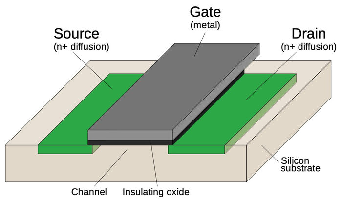
To explain the role of the masks, I'll start with the structure of a metal-gate MOSFET, the transistor used in the Nanoprocessor. At the bottom, two regions of silicon (green) are doped to make them conductive, forming the source and drain of the transistor. A metal strip in between forms the gate, separated from the silicon by a thin layer of insulating oxide. (These layers—Metal, Oxide, Semiconductor—give the MOS transistor its name.) The transistor can be considered a switch controlled by the gate. The metal layer also provides the main wiring of the integrated circuit, although the silicon layer is also used for some wiring.

Structure of a metal-gate MOSFET.

Structure of a metal-gate MOSFET.

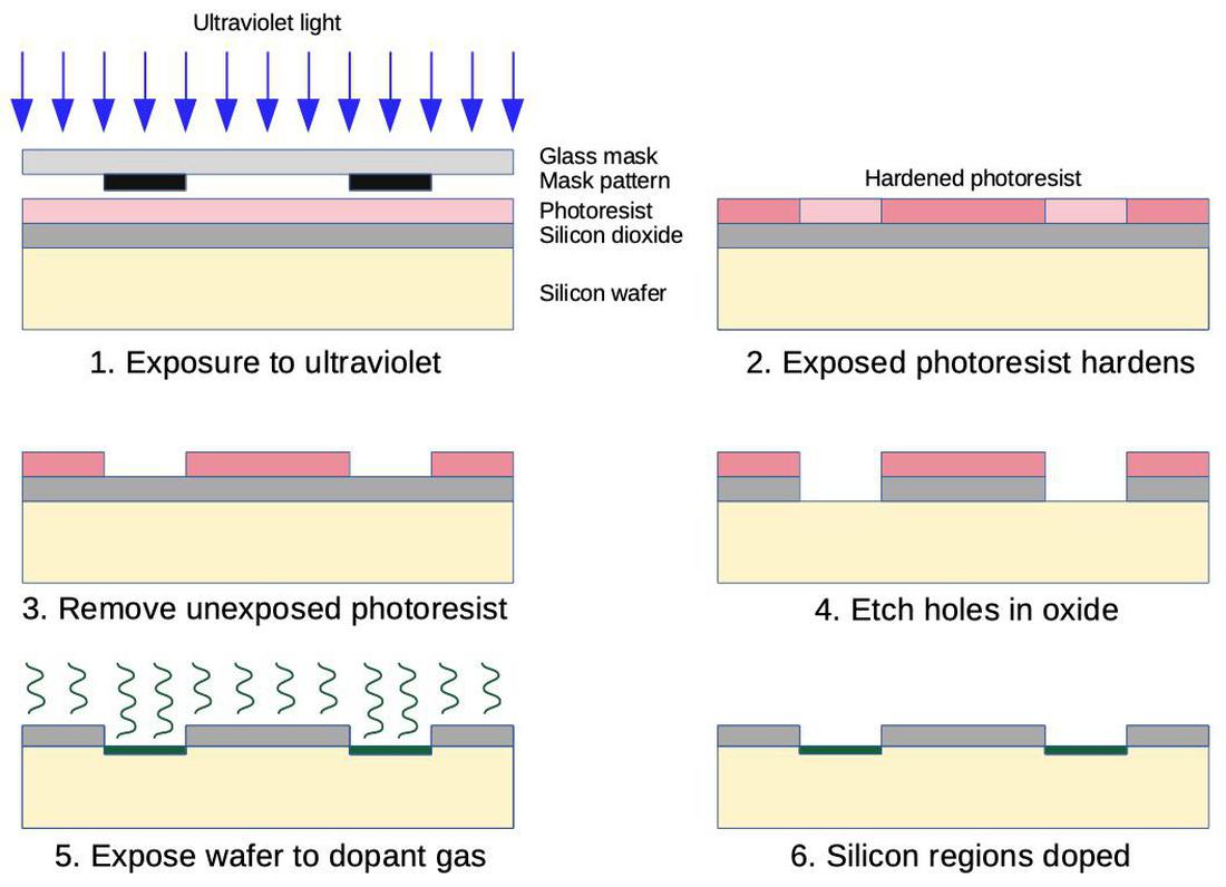
Masks are a key part of the integrated circuit construction process, specifying the position of the components. The diagram below shows how a mask is used to dope regions of the silicon. First, the silicon wafer is oxidized to form an insulating oxide layer on top, and then light-sensitive photoresist is applied. Ultraviolet light polymerizes and hardens the photoresist, except where the mask blocks the light. Next, the soft, unexposed photoresist is dissolved. The wafer is exposed to hydrofluoric acid, which removes the oxide layer where it is not protected by photoresist. This yields holes in the oxide that match the mask pattern. The wafer is then exposed to a high-temperature gas which diffuses into the unprotected silicon regions, modifying the silicon's conductivity. These processing steps create tiny doped silicon regions matching the masks's pattern. As will be shown below, the other masks are used for different processing steps, but using the same photoresist-and-mask process.

How a photomask is used to dope regions of silicon.

How a photomask is used to dope regions of silicon.

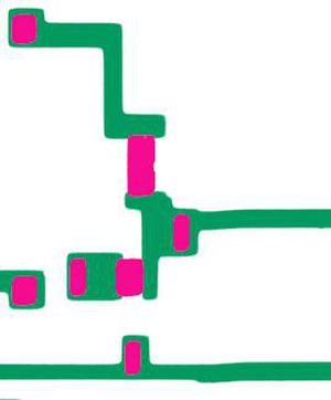
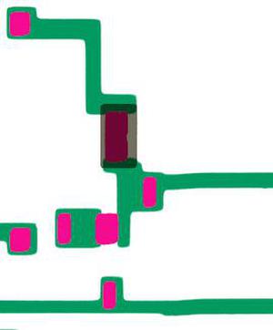
I'll zoom in on the Nanoprocessor's die and show how one of its circuits is constructed from the six masks. (This two-transistor circuit is an inverter, flipping the binary value of its input.) The first mask dopes regions of silicon to make them conductive, using the photolithography steps described above. The doped regions (green) will become transistor source/drains or wiring between components.

The first mask creates conductive silicon regions.

The first mask creates conductive silicon regions.

Next, the die is covered with an insulating oxide layer. The second mask (magenta) is used to etch openings in the oxide, exposing the silicon underneath. These openings will be used to create transistor gates as well as connecting metal wiring to the silicon.

The second mask creates openings in the oxide layer.

The second mask creates openings in the oxide layer.

The third mask (gray) exposes a region to ion implantation, which changes the doping of the silicon, and thus the transistor's properties. This turns the upper transistor into a special depletion-mode transistor that pulls logic gate outputs high.

The third mask is used to increase the doping of the upper transistor.

The third mask is used to increase the doping of the upper transistor.

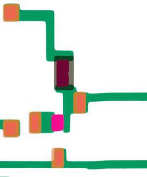
Next, the silicon is covered with an additional thin layer of insulating oxide, forming the gate oxide for the transistors. The fourth mask (orange) removes this oxide from regions that will become contacts between the silicon and the metal layer. After this step, most of the die is covered with a thick insulating oxide layer. The oxide layer is very thin over the transistor gates (magenta), and there are contact holes in the oxide from the current mask (orange).

The fourth mask creates holes in the oxide.

The fourth mask creates holes in the oxide.

The fifth mask (blue) is used to create the metal wiring on top; a uniform metal layer is applied and then the undesired parts are etched off. In locations where the fourth mask created holes in the oxide, the metal layer contacts the silicon and forms a connection. In locations where the third mask created a thin oxide layer, the metal layer forms the transistor gate between two silicon regions. Finally, the entire wafer is covered with a protective glassy layer. The sixth mask (not shown) is used to form holes in this layer over the pads around the edges of each chip. Once the wafer is cut into individual silicon dies (dice?), bond wires are attached to the pads, connecting the die to the external pins.

The fifth mask creates the metal wiring.

The fifth mask creates the metal wiring.

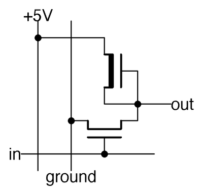
The schematic below shows how the circuitry above forms a two-transistor inverter. The two transistor symbols correspond to the two transistors created by the masks. When there is no input, the upper transistor (connected to +5 volts) pulls the output high. When the input is high, it turns on the lower transistor. This connects the output to ground, pulling the output low. Thus, the circuit inverts the output.

Schematic of an NMOS inverter, corresponding to the masks above.

Schematic of an NMOS inverter, corresponding to the masks above.

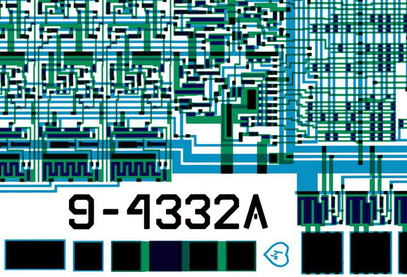
Although the diagrams above show just a single inverter, these masking steps create the entire processor with its 4639 transistors.11 The diagram below shows a larger part of the die with dozens of transistors forming more complex gates and circuitry. One cute thing I noticed on the masks is a tiny heart with HP inside, below the chip's number.14

Chip art: HP inside a heart, below the part number 9-4332A

Chip art: HP inside a heart, below the part number 9-4332A

Controlling a clock with the Nanoprocessor

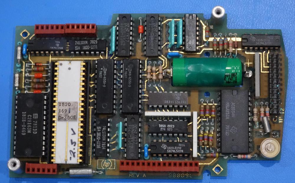
To understand how the Nanoprocessor was used in practice, I reverse-engineered the code from an HP 98035 clock module. This module was plugged into an HP desktop computer15 to provide a real-time clock, as well as millisecond-accurate timings, intervals, and periodic events. The design of the clock module was rather unusual. To preserve the time when the computer was powered-down, the clock module was built around a digital watch chip with a backup battery.17 Inconveniently, the digital watch chip wasn't designed for computer control: it generated 7-segment signals to drive an LED, and it was set through three buttons. To read the time, the Nanoprocessor had to convert the 7-segment display outputs back into digits. And to set the time, the Nanoprocessor had to simulate the right sequence of button presses to advance through the digits.

Nanoprocessor (white chip) as part of an HP clock module. The 2-kilobyte ROM is to the left of the Nanoprocessor.
The two 256-bit×4 RAM chips are to the right.
The Texas Instruments clock chip is the large black chip below the green NiCad battery. Photo courtesy of Marc Verdiell.

Nanoprocessor (white chip) as part of an HP clock module. The 2-kilobyte ROM is to the left of the Nanoprocessor. The two 256-bit×4 RAM chips are to the right. The Texas Instruments clock chip is the large black chip below the green NiCad battery. Photo courtesy of Marc Verdiell.

The host computer controlled the clock module by sending it ASCII strings such as "S 12:07:12:45:00" to set the clock to 12:45:00 on December 7 (or on July 12 if the module was running in European mode). The module's various interval timers, periodic alarms, and counters were controlled with similar commands such as "Unit 2 Period 12345". The module supported 24 different commands, and the Nanoprocessor had to parse them. (See the manual for details.)

Here's some sample code reverse-engineered from the clock board ROM. This code is from the interrupt handler that increases the time and date every second. The code below determines how many days in the current month so it knows when to move to the next month. The columns are the byte value, the corresponding opcode, and my description of the instruction.

This code takes a month number (01-12 BCD) in the accumulator and returns (in register 0) the number of days in the month (28, 30, or 31 BCD). Not bad for 16 bytes of code, even if it ignores leap years. How does it work? For months past 7 (July), it subtracts 1. Then, if the month is odd, it has 31 days, while an even month has 30 days. To handle February, the code clears bit 1 of the month. If the month is now 0 (i.e. February), it has 28 days.

This code demonstrates that even though a processor without addition sounds useless, the Nanoprocessor's bit operations and increment/decrement allow more computation than you'd expect.16 It also shows that Nanoprocessor code is compact and efficient. Many things can be done in a single byte (such as bit test and skip) that would take multiple bytes on other processors.12 The Nanoprocessor's large register file also avoids much of the tedious shuffling of data back and forth often required in other processors. Although some call the Nanoprocessor more of a state machine controller than a microprocessor, that understates the capabilities and role of the Nanoprocessor.

While the Nanoprocessor doesn't include an ALU or have instructions for accessing RAM, these could be added as I/O devices. The clock module has 256 bytes of RAM to hold its multiple counter and timer values, accessed through four I/O ports. Other products added ALU chips to support arithmetic operations.18

Conclusions

The Nanoprocessor is an unusual processor. My first impression was that it wasn't even a "real processor", lacking basic arithmetic functionality. The chip was built with obsolete metal-gate technology, a few years behind other microprocessors. Most bizarrely, each chip required a different voltage, hand-written on the package, suggesting difficulty with manufacturing consistency. However, the Nanoprocessor provided high performance in its microcontroller role, much faster than other processors at the time. Hewlett-Packard used the Nanoprocessor in many products in the 1970s and 1980s, in roles that were more complex than you'd expect. strings and performing calculations.

While the Nanoprocessor has languished in obscurity, without even a mention on Wikipedia, the masks recently revealed by its designer shed light on this unusual corner of processor history. Thanks to Larry Bower for the donation of the masks, John Culver at The CPU Shack for scanning and sharing the masks, and Antoine Bercovici for remastering the masks. Thanks to Marc Verdiell for dumping the clock board ROM.

I plan to write about the internal circuitry of the Nanoprocessor so follow me on Twitter at @kenshirriff for updates on Part II. I also have an RSS feed.

Notes and references

  1. More information on the HP Nanoprocessor and its history is in CPU Shack's recent article The Forgotten Ones: HP Nanoprocessor, as well as at HP9825.com and The HP 9845 Project

  2. I'm not completely comfortable calling the Nanoprocessor a microcontroller since it uses an external program ROM, while a microcontroller usually has everything, including the ROM, on a single chip. (It is like the Intel 4004 in this way.) However, the Nanoprocessor resembles a microcontroller in most ways: it is designed for embedded control applications, with a Harvard architecture and an instruction set optimized for I/O, running a program from ROM with minimal storage. 

  3. On the topic of computers that can't add, the desk-sized IBM 1620 computer (1959) didn't have addition circuitry, but used table lookup for addition. It had the codename CADET; people joked that this stood for "Can't Add, Doesn't Even Try." 

  4. I've determined that the Nanoprocessor was used in the following HP products (and probably others): HP 9845B, HP 3585A spectrum analyzer, HP 3325A Synthesizer / Function Generator, HP 9885 floppy disk drive, HP 3070B data capture terminal, HP 98034 HPIB interface for the HP 9825 calculator, HP 98035 real time clock for the HP 9825 desktop computer, HP 7970E tape drive interface, HP 4262A LCR meter, HP 3852 Spectrum Analyzer, and HP 3455A voltmeter. Poul-Henning Kamp informs me that the HP 3336 Synthesizer / Function Generator and HP 9411 Switch Controller also used the Nanoprocessor. I've also been informed that the HP3437A System Voltmeter uses the Nanoprocessor. 

  5. The mask images can be downloaded here (warning: 122 MB PSD file). 

  6. The Nanoprocessor is like a RISC (Reduced Instruction Set Computer) processor in many ways, although it predated the RISC concept by several years. In particular, the Nanoprocessor is designed with a simple opcode structure, all instructions execute in one cycle (after the fetch cycle), the register set is large and orthogonal, and addressing is simple. These RISC characteristics yielded a high clock speed compared to more complex processors. 

  7. Interestingly, the Nanoprocessor's competition during development was the Motorola 6800, rather than an Intel processor. The Nanoprocessor's key feature was performance: it ran at 4 MHz, compared to 1 MHz for the 6800. (Both processors took 2 cycles to perform a basic instruction, while the 6800 took up to 7 cycles for more complex instructions.)

    The Nanoprocessor designers wrote a timing comparison, estimating that the Nanoprocessor could count six times faster than the 6800 and handle interrupts over sixteen times faster. The proposal assumed a 5 MHz Nanoprocessor while the actual chip fell a bit short, running at 4 MHz. The projected cost of the Nanoprocessor was $15 per chip, compared to $360 for the Motorola 6800. 

  8. I'm impressed with the density of the Nanocomputer's layout given its limitations: one layer of metal wiring and no polysilicon. I've looked at other metal-gate chips and their layouts are horribly inefficient, with a lot more wiring than transistors. However, the Nanoprocessor's circuits are arranged efficiently, with very little wasted space. 

  9. The Nanoprocessor's fabrication technology was ahead of the Intel 8080 and Motorola 6800 in one way: it used depletion-mode pull-up transistors, more advanced than the enhancement-mode transistors in the 8080 and 6800. Depletion-mode transistors resulted in faster, lower-power logic gates, but required an additional manufacturing step. For the Nanoprocessor, this step used mask #3 (the gray mask). In processors such as the MOS Technology 6502 and Zilog Z-80, depletion-mode transistors allowed the processor to run off a single voltage instead of three. Unfortunately, the Nanoprocessor still required three voltages due to its metal-gate transistors. 

  10. Early DRAM memory chips and microprocessor chips often required three supplies: +5V (Vcc), +12V (Vdd) and -5V (Vbb) bias voltage. In the late 1970s, improvements in chip technology allowed a single supply to be used instead. The Intel 8080 microprocessor (1974) used enhancement-mode transistors and required three voltages, but the improved 8085 (1976) used depletion-mode transistors and was powered by a single +5V supply. Starting in the late 1970s, many microprocessors used an on-chip charge pump to generate the negative bias voltage. I wrote about the 8086's charge pump here

  11. By my count, the Nanoprocessor has 4639 transistors. The instruction decoder is constructed from pairs of small transistors for layout reasons; combining these pairs yields 3829 unique transistors. Of these, 1061 act as pull-ups, while 2668 are active. In comparison, the 6502 has 4237 transistors, of which 3218 are active. The 8008 has 3500 transistors and the Motorola 6800 has 4100 transistors. 

  12. Early microprocessors didn't have bit set, reset, and test operations (although these could be accomplished with AND and OR). The Z-80 (1976) added bit operations, but they took two bytes and were much slower than the Nanoprocessor. 

  13. The Nanoprocessor sticks to its model of executing the instruction in one cycle even for two-byte instructions: The second byte is fetched during the execute cycle, so the overall timing is unchanged. 

  14. The Nanoprocessor has two different part numbers. The 1820-1691 was the 2.66 MHz version, while the 1820-1692 was the 4 MHz version. The last digit of the part number was hand-written on each chip after testing its performance. (The part number is unrelated to the chip's number 9-4332A on the die.) 

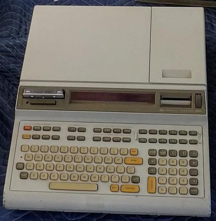
  15. The HP 9825 was a 16-bit desktop computer, running a BASIC-like language. It was introduced in 1976, five years before the IBM PC, and was a remarkably advanced system for its time. The back of the HP 9825 had three I/O slots for adding modules such as the real time clock.

    An HP 9825 with tape drive, LED display, and printer. From Marc Verdiell's collection.

    An HP 9825 with tape drive, LED display, and printer. From Marc Verdiell's collection.


  16. I came across one place in the code where it needs to add two BCD digits to form one byte. This was accomplished by a loop that decremented one number while incrementing the second. When the first number reached zero, the result was the sum. Thus, even without an ALU, addition is possible but slow. 

  17. The Texas Instruments watch chip was implemented with Integrated Injection Logic (I2L) to keep power consumption low. Nowadays, a low-power chip would use CMOS, but that wasn't common at the time. Integrated Injection Logic was built from bipolar transistors, similar to TTL, but using different high-density, low-power circuitry. I discussed Integrated Injection Logic in detail in this blog post. The Texas Instruments chip may be the X-902 in a DIP package. 

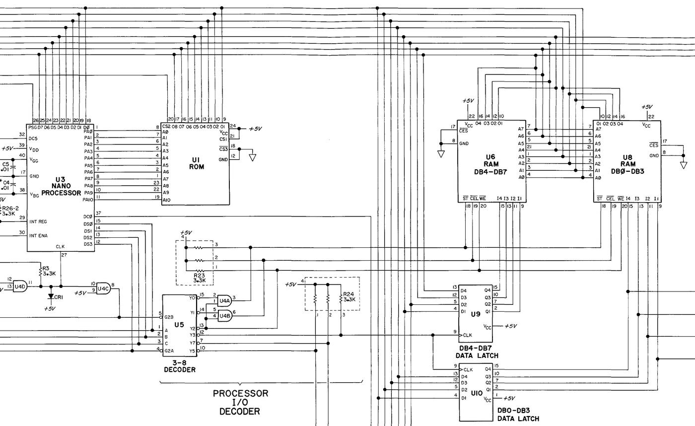
  18. The clock board schematic shows how the two 256×4 RAM chips are connected to the Nanoprocessor. The Nanoprocessor's I/O port select pins are connected to the "3-8 Decoder" U5, which produces a separate signal for each I/O port. Three of these signals go to the RAM chip's control pins, while one signal controls the Data Latch chips U9 and U10 that hold write data.

    RAM chips connected to the Nanoprocessor. From the Clock service manual.

    RAM chips connected to the Nanoprocessor. From the Clock service manual.

    All I/O ports use the Nanoprocessor's data bus (top) for communication, so the data bus is connected to both the address and data pins of the RAM chips. For a read, the RAM address is written to the RAM chips via one I/O port and then the data is read from RAM via a second port. In both cases, the values go across the data bus, while the signal from the "3-8 Decoder" indicates what to do with the values. For a write, the first I/O operation stores the byte value in the latches, and then the second I/O operation sends the address to the RAM chips. While this may seem like a clunky, Rube-Goldberg approach, it works well in practice; a read or write can be done with two bytes of instructions.

    (Many processors, such as the 6502, used memory-mapped I/O; I/O devices were mapped into the memory address space and accessed through memory read/write operations. The Nanoprocessor is the opposite, putting RAM into the I/O port space and accessing it through I/O operations.)

    Adding an ALU uses a similar approach, as in the HP 3455A voltmeter (schematic), which contains two Nanoprocessors. The voltmeter uses two 74LS181 ALU chips to implement an 8-bit ALU that it uses to scale value and compute percentage error. Two output ports provide the arguments and another port specifies the operation. The 8-bit result is read from a port, while the processor reads the carry through a GPIO pin. (At this point, I'd wonder if it wouldn't be better to use a processor that includes arithmetic.) 

Reverse-engineering the 8086's Arithmetic/Logic Unit from die photos

The Intel 8086 processor was introduced in 1978, setting the course of modern computing. While the x86 processor family has supported 64-bit processing for decades, the original 8086 was a 16-bit processor. As such, it has a 16-bit arithmetic logic unit (ALU).1 The arithmetic logic unit is the heart of a processor: it performs arithmetic operations such as addition and subtraction. It also carries out Boolean logic operations such as bitwise AND and OR as well as also bit shifts and rotates. Since a fast ALU is essential to the overall performance of a processor, ALUs often incorporate interesting design tricks.

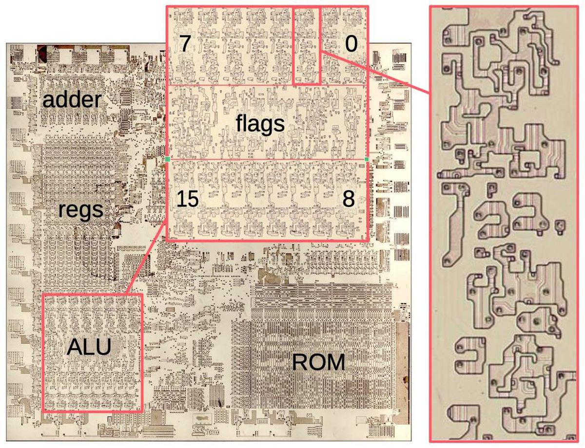
The die photo below shows the silicon die of the 8086 processor. The ALU is in the lower-left corner. Above it are the general- and special-purpose registers. An adder, used for address calculation, is in the upper left. (For performance, the 8086 has a separate adder to add the segment register and memory offset when accessing memory.) The large microcode ROM is in the lower right.

The 8086 die, zooming in on one bit of the ALU. The metal and polysilicon layers were removed for this photo, showing the silicon layer.

The 8086 die, zooming in on one bit of the ALU. The metal and polysilicon layers were removed for this photo, showing the silicon layer.

Zooming in on the ALU shows that it is constructed from 16 nearly-identical stages, one for each bit. The upper row handles bits 7 to 0 while the lower row handles bits 15 to 8.3 In between, the flag circuitry indicates the status of an arithmetic operation through condition codes such as zero or nonzero, positive or negative, carry, overflow, parity, and so forth. These are typically used for conditional branches.

In this blog post, I reverse-engineer the 8086's ALU and explain how it works. It's more complex than other vintage ALUs that I've studied,2 using a flexible circuit that can implement arbitrary bit functions. The carry is implemented with a Manchester carry chain, a fast design dating back to a 1960s supercomputer.

The ALU circuitry

The 8086's ALU circuitry is a bit tricky, so I'll start by explaining how it adds two numbers. If you've studied digital logic, you may be familiar with the full adder, a building-block for adding binary numbers. Specifically, a full adder takes two bits and a carry-in bit. It adds these three bits and outputs the 1-bit sum, as well as a carry-out bit. (For instance 1+0+1 = 10 in binary, so the carry-out is 1 and the sum bit is 0.) A 16-bit adder can be created by joining 16 full-adders, with the carry-out from one fed into the carry-in of the next.

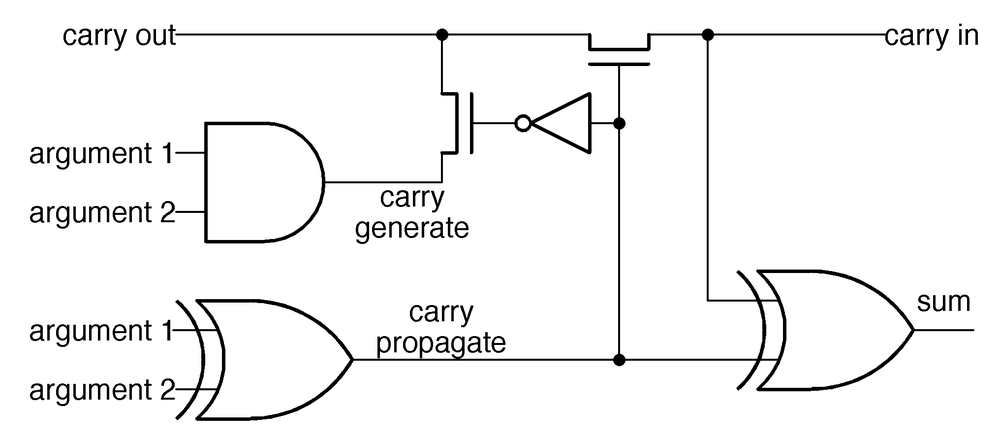
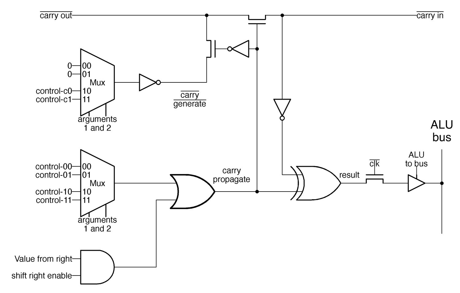
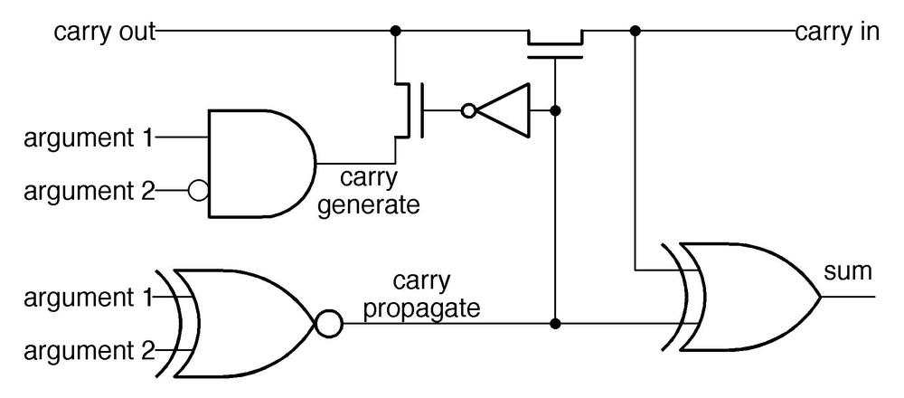
The simplified diagram below represents one stage of the ALU's adder. It takes two inputs and the carry-in and sums them, forming a 1-bit sum output and a carry-out. (Note that the carry signal travels right-to-left.) The sum bit output is generated by the exclusive-or of the two arguments and the carry-in, using the two exclusive-or gates at the bottom. Generating the carry, however, is more complex.

A simplified diagram of the 8086 ALU, showing how it performs addition. Two transistors control the carry-out.

A simplified diagram of the 8086 ALU, showing how it performs addition. Two transistors control the carry-out.

The carry computation uses an optimization called the Manchester carry chain4, dating back to 1959, to avoid delays as the carry ripples from one stage to the next. The idea is to decide, in parallel, if each stage will generate a carry, propagate an existing carry, or block an incoming carry. Then, the carry can rapidly flow through the "carry chain" without sequential evaluation. To understand this, consider the cases when adding two bits and a carry-in. For 0+0, there will be no carry-out, regardless of any carry-in. On the other hand, adding 1+1 will always produce a carry, regardless of any carry-in; this case is called "carry-generate". The interesting cases are 0+1 and 1+0; there will be a carry-out if there was a carry-in. This case is called "carry-propagate" since the carry-in propagates through the stage unchanged.

In the Manchester carry chain, the carry-propagate signal opens or closes transistors in the carry line. In the carry-propagate case, the top transistor is activated, connecting carry-in to carry-out, so the carry can flow through. Otherwise, the lower transistor is activated and the carry-out receives the carry-generate signal, generating a carry if both arguments are 1. Since these transistors can all be set in parallel, carry computation is quick. There is still some propagation delay as the carry signal flows through the transistors in the carry chain, but this is much faster than computing the carry through a sequence of logic gates.5

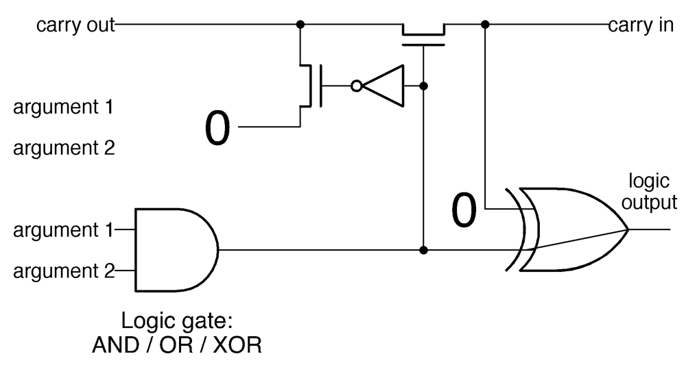
That explains how the ALU performs addition,6 but what about logic functions? How does it compute AND, OR, or XOR? Suppose you replace the carry-propagate XOR gate with a logic gate (AND, OR, or XOR) and replace the carry-generate gate with 0, as shown below. The output will simply be the AND (or OR or XOR) of the two arguments, depending on the new gate. (The right XOR gate has no effect since XOR with 0 passes the value through unchanged.) The point is that if you could somehow replace the gates, the same circuit could compute the AND, OR, and XOR logic functions, as well as addition.

To compute a logic function, the XOR gate is (conceptually) replaced by a different logic gate, and the carry-generation is blocked.

To compute a logic function, the XOR gate is (conceptually) replaced by a different logic gate, and the carry-generation is blocked.

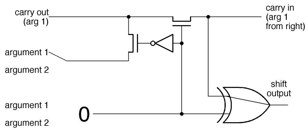
Another important operation is bit shifting. The ALU shifts a value to the left by taking advantage of the carry line in an unusual way (below).7 The bit from the first argument is directed into the carry-out, sending it one bit position to the left. The received carry bit passes through the XOR gate, resulting in a left shift by one bit. The carry-propagate signal is set to 0; this both directs the argument bit to carry-out, and turns the XOR gate into a pass-through. (A right shift is implemented with a separate circuit, as will be explained below.)

Shifting left by one bit takes advantage of the carry line to pass each bit to the left.

Shifting left by one bit takes advantage of the carry line to pass each bit to the left.

Thus, the ALU can reuse this circuit to perform a variety of operations, by reprogramming the carry-propagate and generate gates with different functions. But how are these magic reprogrammable gates implemented? The trick is that any Boolean function of two variables can be specified by the four values in the truth table. For instance, AND has the truth table below, so it can be specified by the four values: 0, 0, 0, 1:

ABA AND B
000
010
100
111

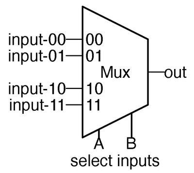
If we feed those values into a multiplexer, and select the desired value based on the two inputs, we will get the AND of the inputs. If instead, we feed 0, 1, 1, 0 into the multiplexer, we will get the XOR of the inputs. Other inputs create other logic functions similarly. With the appropriate values, any logic function of two variables can be implemented.8 (Some special cases: 0, 0, 0, 0 will output the constant 0; while 0, 0, 1, 1 will output the input A. This multiplexer circuit is used for the carry-propagate gate. A similar but half-sized circuit is used for the carry-generate gate.9

A multiplexer acts as a generic gate in the ALU.

A multiplexer acts as a generic gate in the ALU.

Now that I've presented the background, the complete ALU circuit is shown below, with multiplexers in place of the carry-propagate and generate gates. On the chip, the carry-in and carry-out are inverted, and this is reflected below. The schematic also shows the connection from the ALU to the bus, outputting the result. The circuitry at the bottom supports the shift right operation, which doesn't fit into the general circuit of the ALU. For this blog post, I'll ignore how the control signals are generated.10

One bit of the ALU circuitry in the 8086.

One bit of the ALU circuitry in the 8086.

The ALU's implementation in silicon

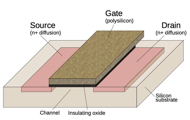
The 8086 and other processors of that era were built from a type of transistor called NMOS. The silicon substrate was "doped" by diffusion of arsenic or boron to form conductive silicon and transistors. On top of the silicon, polysilicon wiring created the gates of the transistors and wired components together. Finally, a metal layer on top provided more wiring. (In comparison, modern processors are built from CMOS technology, which combines NMOS and PMOS transistors, and they have many layers of metal wiring.)

Structure of an NMOS transistor (MOSFET) as implemented in an integrated circuit.

Structure of an NMOS transistor (MOSFET) as implemented in an integrated circuit.

The diagram above shows the structure of an NMOS transistor. The transistor can be viewed as a switch, allowing current to flow between two diffusion regions called the source and drain. The transistor is controlled by the gate, made of a special type of silicon called polysilicon. A high voltage on the gate lets current flow between the source and drain, while low voltage on the gate blocks the current flow.

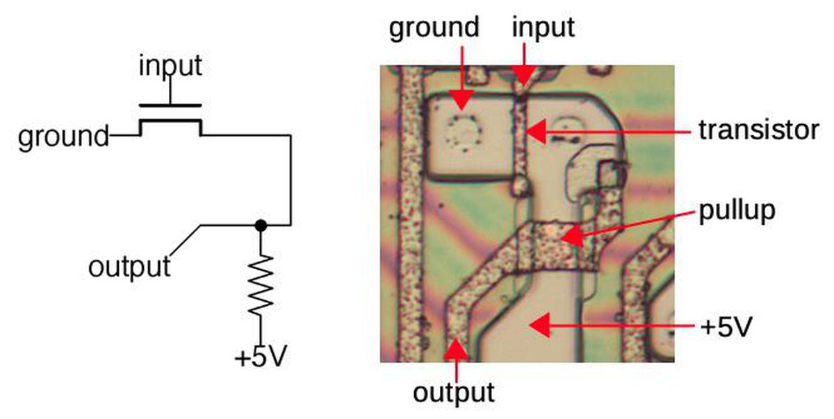
The simplest logic gate is an inverter; the diagram below shows how an inverter is built from an NMOS transistor and a resistor.11 The pinkish regions are doped silicon, while the brownish lines are the polysilicon wiring on top. A transistor is formed where the polysilicon line crosses the doped silicon. With a low input, the transistor is off, so the pull-up resistor pulls the output high. With a high input, the transistor turns on. This connects the output to ground, pulling the output low. Thus, the input signal is inverted.

An inverter, as implemented in the 8086's ALU.

An inverter, as implemented in the 8086's ALU.

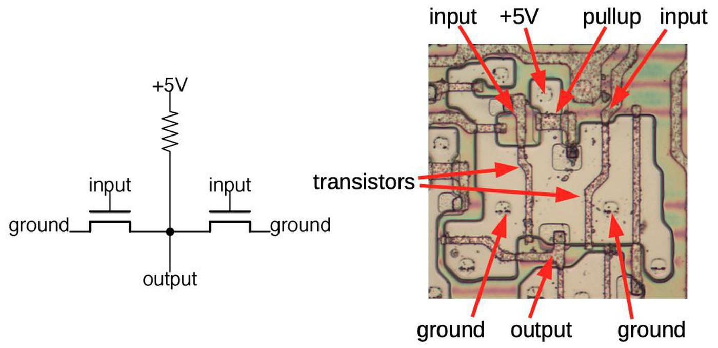
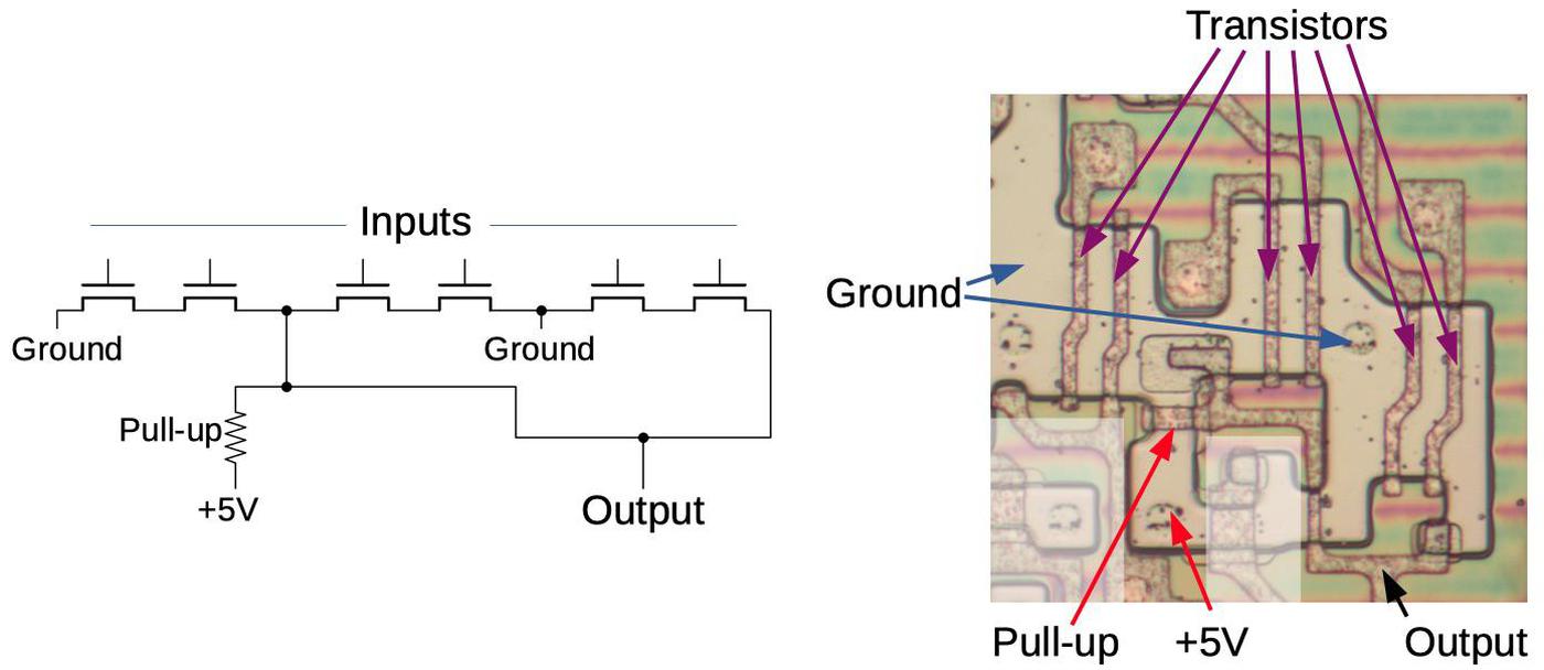
A more complex gate, such as the 2-input NOR gate below, uses similar principles. With low inputs, the transistors are turned off, so the pullup resistor pulls the output high. If either input is high, the corresponding transistor turns on and pulls the output low. Thus, this circuit implements a NOR gate. The die layout matches the schematic, but has a complicated appearance due to space-saving optimization. You might expect the transistors to be simple rectangles, but the silicon regions have irregular shapes to make the most use of the space. In addition, other transistors (not part of the NOR gate) share the ground connections to save space.

A NOR gate as implemented in the 8086's ALU. The metal wiring has been removed for this photo, showing the silicon and polysilicon underneath.

A NOR gate as implemented in the 8086's ALU. The metal wiring has been removed for this photo, showing the silicon and polysilicon underneath.

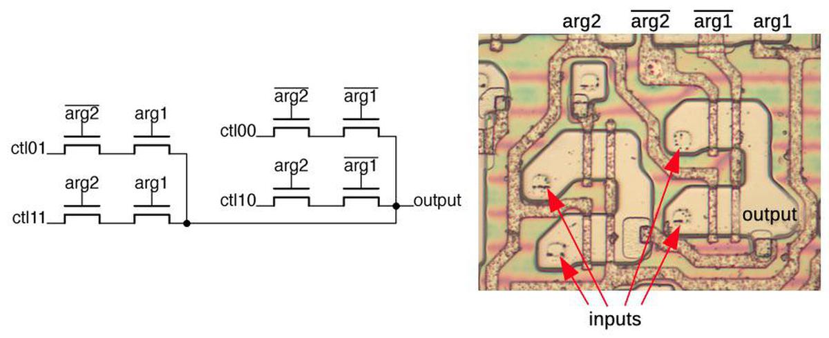
The multiplexers are built using a completely different technique: pass transistors. Instead of pulling the output to ground, pass transistors pass an input signal through to the output. In the multiplexer, each input is connected to a different pair of transistors. Depending on the arguments, exactly one pair will have both transistors on. For instance, if arg2 is 0 and arg1 is 1, the transistor pair in the upper left will connect ctl01 to the output. Each other input will be blocked by a transistor that is turned off. Thus, the multiplexer selects one of the four inputs, passing it through to the output. (This pass-transistor approach is more compact than building a multiplexer out of standard logic gates.)

Implementation of the multiplexed gate in the ALU.

Implementation of the multiplexed gate in the ALU.

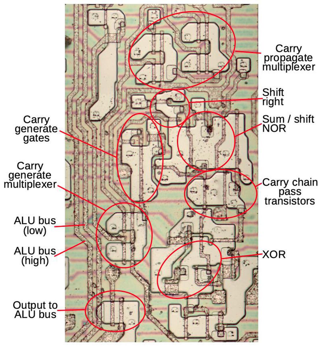
The diagram below shows an ALU stage with the major components labeled. You may spot the inverter, NOR gate, and multiplexer described earlier. Other components are implemented with similar techniques. This diagram can be compared with the earlier schematic. The reddish horizontal lines are remnants of the metal layer, which was removed for this photo. These lines carried the control signals, power, and ground.

Die photo of ALU with main components labeled.

Die photo of ALU with main components labeled.

The ALU's temporary registers

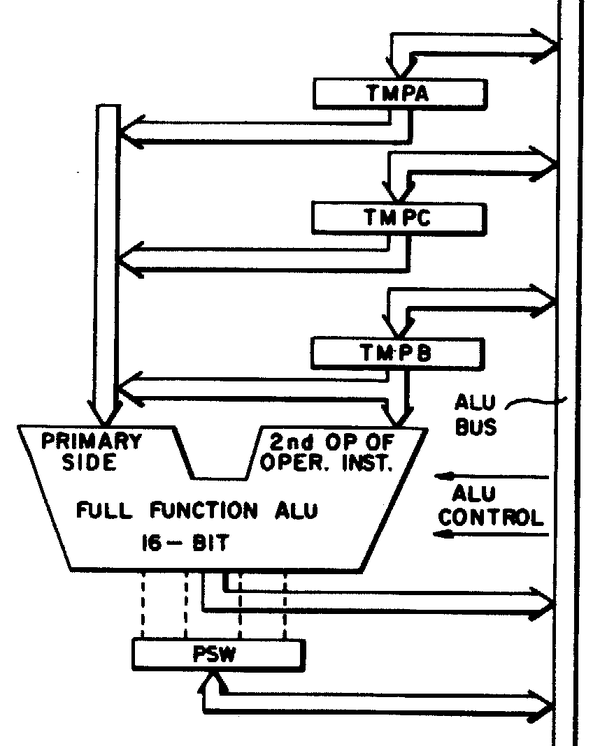
The diagram below (from the 8086 patent) shows how the ALU is connected to the rest of the processor by the ALU bus. The discussion above covered the "Full Function ALU" in the middle of the diagram, which takes two 16-bit inputs and produces a 16-bit output. These inputs are supplied from three temporary registers: A, B, and C. (These temporary registers are invisible to the programmer and should not be confused with the 8086's AX, BX, and CX registers.) I'll mention a few features of these registers that will be important later. Any register can provide the ALU's first input, but the second input always comes from the B register. These registers have a bidirectional connection to the ALU bus, so they can be both written and read. One unusual feature of the ALU is that it has a single data connection to the rest of the 8086, through the ALU bus.12 This seems like a bottleneck, since two clock cycles are required to load the registers, followed by another clock cycle to access the result. But apparently the single bus worked well enough for the 8086.

This diagram from the 8086 patent shows the ALU and its associated registers.

This diagram from the 8086 patent shows the ALU and its associated registers.

The Processor Status Word (PSW) shown above holds the condition flags, status bits on the ALU result: zero, negative, overflow, and so forth. Although the PSW looks trivial in the diagram above, the die photo at the top of the article shows that it constitutes about a third of the ALU circuitry. I'll leave the flag circuitry for a later discussion due to its complexity: each flag has unique circuitry that handles many special cases.

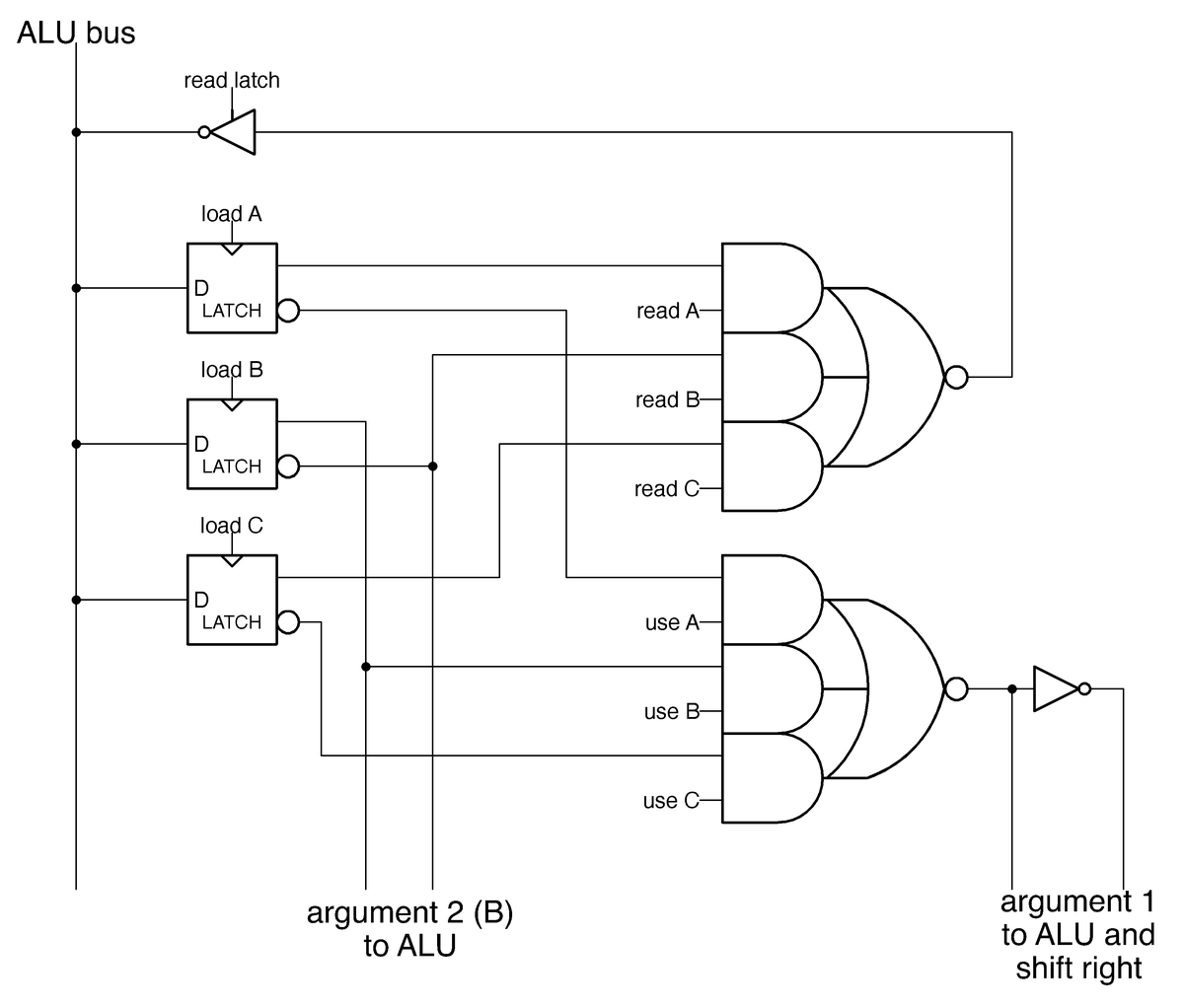
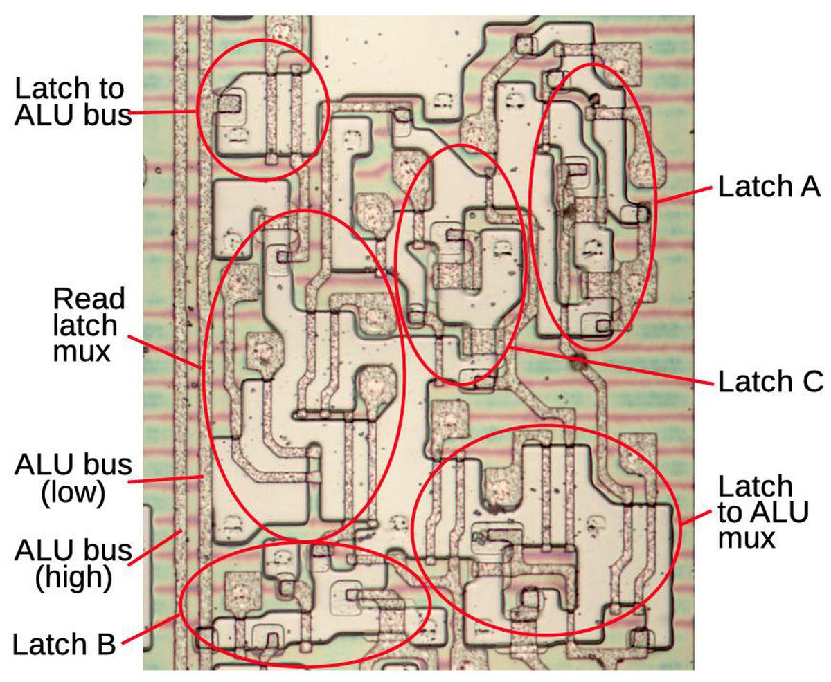
The schematic below shows one bit of the reverse-engineered implementation of the ALU's temporary registers. The registers are implemented with latches; each box represents a latch, a circuit that holds one bit. The two large AND-NOR gates act as multiplexers, selecting the output from one of the latches. The upper gate selects one of the registers for reading. The lower gate selects one of the registers as an argument for the ALU.

This circuit implements the ALU's three temporary registers and the associated circuitry.

This circuit implements the ALU's three temporary registers and the associated circuitry.

While the 6-input AND-NOR gate multiplexer may look complex, it is straightforward to implement with NMOS transistors. The schematic shows how it is built from 6 transistors and a pull-up. You can verify that if both transistors in a pair are energized, the output will be pulled to ground, providing the AND-NOR function.

The 6-input AND-NOR gate is built from 6 transistors, arranged in pairs.

The 6-input AND-NOR gate is built from 6 transistors, arranged in pairs.

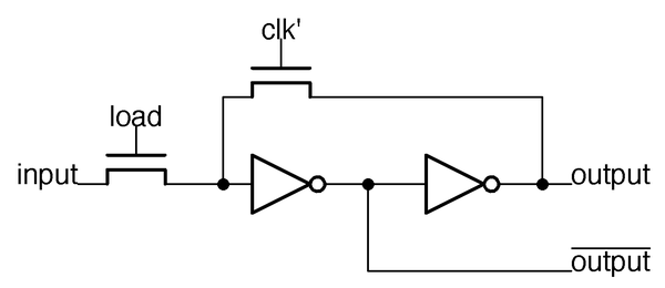
The latch circuit is shown below. I've written about the 8086's latches in detail, so I'll give just a quick summary. The idea of the latch is that it can stably hold either a 0 or a 1 bit. When the clock signal clk' is high, the upper transistor is on, connecting the inverters into a loop. If the input to the first inverter is 1, it outputs a 0 to the second inverter, which outputs a 1 to the first, so they stay in that state, storing the bit. Similarly, the loop is stable if the input is a 0.

A one-bit latch in the 8086's ALU.

A one-bit latch in the 8086's ALU.

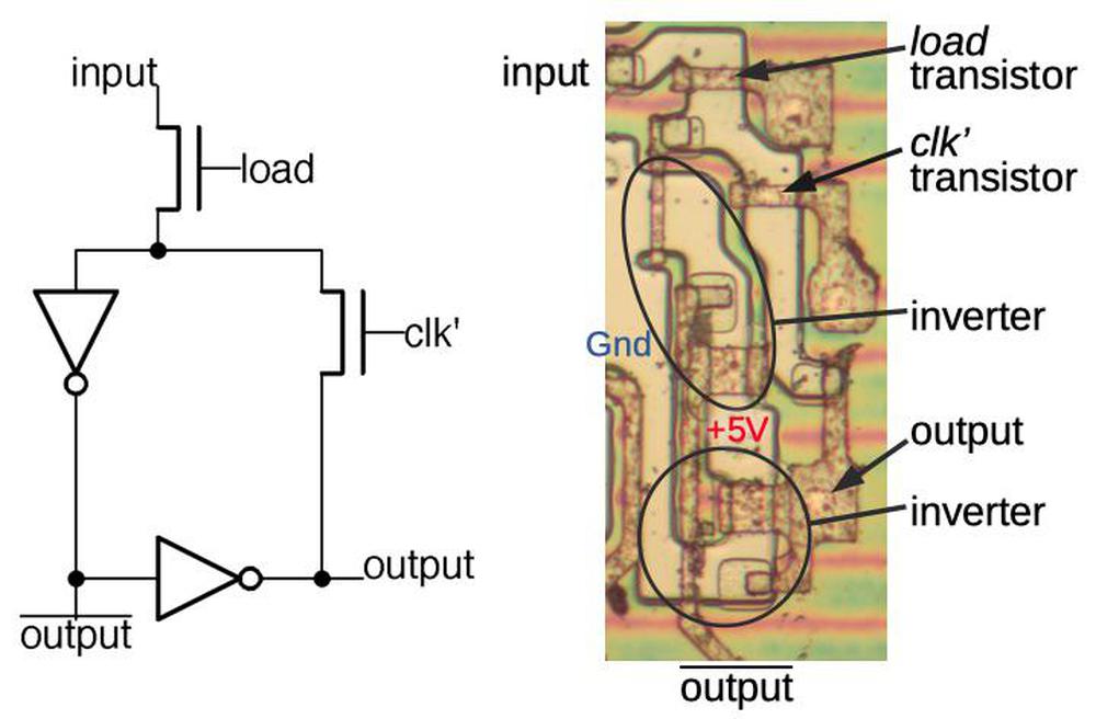
The special thing about this latch is that it's a dynamic latch. When the clock signal clk' is low, the loop is broken, but the input on the first inverter remains, due to the capacitance of the wire and transistor. When clk' goes high again, this voltage is refreshed. Alternatively, when clk' is low, a new value can be loaded into the latch by activating load, turning on the first transistor and allowing a new input signal to pass into the latch. The 8086 uses dynamic latches because the latch is compact, using just two transistors and two inverters. The latch is implemented in silicon as shown below.

Implementation of a latch in the 8086's ALU.

Implementation of a latch in the 8086's ALU.

The diagram below summarizes the components of the temporary register implementation. This circuitry is repeated 16 times to complete the registers.13 The output from the registers is fed into the ALU circuitry described earlier.

The ALU uses three temporary registers to hold arguments. This diagram shows the implementation of one bit.

The ALU uses three temporary registers to hold arguments. This diagram shows the implementation of one bit.

Conclusions

Although the Intel 8086 has complex circuits, its features are large enough that it can be studied under a microscope. The ALU is a key part of the processor and takes up a large fraction of the die. Its circuitry can be reverse-engineered through careful examination, revealing its interesting construction. It uses a Manchester carry chain for fast carry propagation. The carry-generate and carry-propagate signals are created by multiplexers that operate as arbitrary function generators, creating a flexible ALU with a small amount of circuitry. The ALU is built from a combination of standard logic, pass-transistor logic, and dynamic logic to optimize performance and minimize size.

You might have noticed that the 8086's ALU doesn't have support for multiplication, division, or multiple-bit shifts, even though the 8086 has instructions for these operations. These operations are computed in microcode using simpler ALU operations (shift, add, subtract for multiplication and division, and repeated single-bit shifts for larger shifts).

Some features of the ALU remain to be described, in particular the condition flags and how the ALU control signals are generated from opcodes. I plan to write about these soon, so follow me on Twitter @kenshirriff or RSS for updates.

Notes and references

  1. The ALU size almost always matches the processor word size, but there are exceptions. Notably, the Z-80 is an 8-bit processor but has a 4-bit ALU. As a result, the Z-80's ALU runs twice for each arithmetic operation, processing half the byte at a time. Some early computers used a 1-bit ALU to keep costs down, but these serial processors were slow. 

  2. I've looked at the ALU of various other early microprocessors including the 8008, Z-80, and the 8085. I've also reverse-engineered the 74181 and Am2901 ALU chips. 

  3. The ALU's layout has bits 15-8 in the top and bits 7-0 below. This layout is a consequence of the bit ordering in the data path: the bits are interleaved 15-7-14-6-...-8-0, instead of linearly 15-14-...-0. The reason behind this interleaving is that it makes it easy to swap the two bytes in the 16-bit word, by swapping pairs of bits. The ALU is split into two rows so it fits into the horizontal space available. Even with the tall, narrow layout of an ALU stage, a bit of the ALU is wider than a bit of the register file. Splitting the ALU into two rows keeps the bit spacing approximately the same, avoiding long wires between the register file and the ALU. 

  4. The Manchester carry chain was developed by the University of Manchester and described in the article Parallel addition in digital computers: a new fast 'carry' circuit, 1959. It was used in the Atlas supercomputer (1962). 

  5. The ALU also uses carry-skip techniques to speed up carry calculation; I'll briefly summarize. The idea of carry-skip is to skip over some of the stages in the carry chain if possible, reducing the worst-case delay through the chain. For example, if there is a carry-in to bit 8, and the carry-propagate is set for bits 8, 9, 10, and 11, then it can be immediately determined that there is a carry-in to bit 12. Thus, by ANDing together the carry-in and the four carry-propagate values, the carry-in to bit 12 can be calculated immediately for this case. In other words, the carry skips from bit 8 to bit 12. Likewise, similar carry-skip circuits allow the carry to skip from bit 2 to bit 4, and bit 4 to bit 8. These carry-skip circuits reduced the ALU's worst-case computation time. The carry-skip circuitry explains why each stage in the ALU is similar but not quite identical. Note that for logic operations or shift, either carry-propagate or carry-generate is 0, so the carry-skip won't activate and corrupt the result. 

  6. I should mention how subtraction is handled. A typical ALU inverts one of the inputs before adding, reusing the addition circuitry for subtraction. However, the 8086's ALU implements subtraction by changing the inputs to the multiplexers, as shown below. This leverages the general-purpose multiplexer and avoids implementing separate negation circuitry. (The comparison operation is implemented as subtraction but without storing the result. If the difference is zero, the values are equal, while a positive difference indicates the first value is larger.)

    Subtraction is similar to addition, but with the second argument negated. This is accomplished by inverting one input of the carry-generate AND gate and changing the carry-propagate XOR to XNOR.

    Subtraction is similar to addition, but with the second argument negated. This is accomplished by inverting one input of the carry-generate AND gate and changing the carry-propagate XOR to XNOR.


  7. The typical way a processor implements a left shift by one bit is by adding the value to itself. I don't know why the 8086 used the carry approach rather than the adding approach. 

  8. An FPGA (field-programmable gate array) uses similar techniques to implement arbitrary logic functions. The truth table is stored in a lookup table (LUT). These lookup tables are typically larger; a 6-input lookup table has 26 = 64 entries. One difference between the FPGA and the ALU is that the FPGA is programmed and then the gate functions are fixed, while the ALU's gates can change functions every operation. 

  9. The carry-generate multiplexer returns 0 if argument 1 is 0. In other words, it only implements two cases of the truth table and has two control inputs. To handle the other two cases, it is pulled low by the clock signal so it outputs 0. Because it is driven by the clock and depends on the value held by the circuit capacitance, it is a form of dynamic logic. The 8086 primarily uses standard static logic, but uses dynamic logic in some places. 

  10. The control signals for the ALU are generated from a PLA (similar to a ROM) that takes a 5-bit opcode as input. This opcode can either come from the instruction or be specified by the microcode. For an instruction, the ALU portion of the instruction is typically bits 5-3 of the first byte of the instruction or bits 5-3 of the MOD R/M byte. The point of this is that one microcode routine can handle all the similar arithmetic/logic instructions, making the microcode smaller. The ALU control PLA generates the signals to perform the correct ALU operation, transparently to the microcode. I should mention that there are many more ALU control signals than I described. Many of these control the flag handling, while others control various special cases.

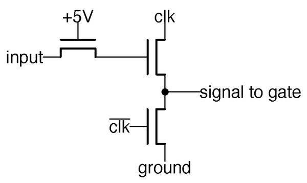
    The control signals pass through the peculiar circuit below. If the input is high, it sends a clock pulse to the ALU. Otherwise, it remains low. The drive signal is discharged to ground on the negative clock phase by the lower transistor. In the absence of an input, the signal is not driven during the positive clock phase, but remains low due to dynamic capacitance. One mystery is the transistor with its gate tied to +5V, leaving it permanently on, which seems pointless. It will reduce the voltage to the gate of the clk transistor, and thus the output voltage, but I don't see why. Maybe to reduce current? To slow the signal?

    The drive signals to the ALU gates are generated with this dynamic circuit.

    The drive signals to the ALU gates are generated with this dynamic circuit.


  11. The pull-up resistor in an NMOS gate is implemented by a special depletion-mode transistor. The depletion-mode transistor acts as a resistor but is more compact and performs better than an actual resistor. 

  12. In the 6502, the two inputs of the ALU are connected to separate buses (details), so they can both be loaded at the same time. The 8085 (and many other early microprocessors) connect the accumulator register to one input of the ALU to avoid use of the bus (details). 

  13. The silicon implementation of the lower eight bits of the ALU / registers is flipped compared to the upper eight bits. The motivation is to put the ALU signals next to the flag circuitry that needs these signals. Since the flag circuitry is sandwiched between the two halves of the ALU, the two halves become (approximate) mirror images. (See the die photo at the top of the article.) 

Inside a counterfeit 8086 processor

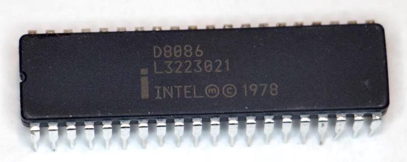
Intel introduced the 8086 processor in 1978, leading to the x86 architecture in use today. I'm currently reverse-engineering the circuitry of the 8086 so I've been purchasing vintage 8086 chips off eBay. One chip I received is shown below. From the outside, it looks like a typical Intel 8086.

The package of the fake 8086. It is labeled as an Intel 8086 from 1978.

The package of the fake 8086. It is labeled as an Intel 8086 from 1978.

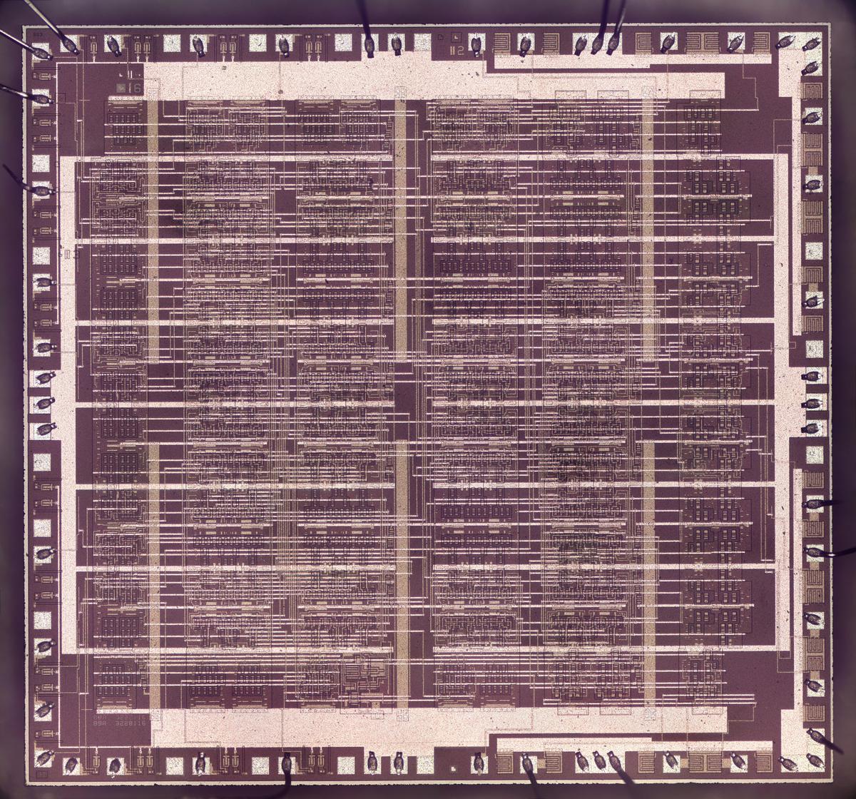
I opened up the chip and looked at it under the microscope, creating the die photo below. The whitish lines are the metal layer, connecting the chip's circuitry. Underneath, the silicon has a purple hue. Around the outside of the die, bond wires connect the square pads to the 40 external pins on the IC.

Die photo of the fake 8086, showing the metal layer on top. The thick horizontal and vertical strips provide power and ground, while the other wiring connects the components.

Die photo of the fake 8086, showing the metal layer on top. The thick horizontal and vertical strips provide power and ground, while the other wiring connects the components.

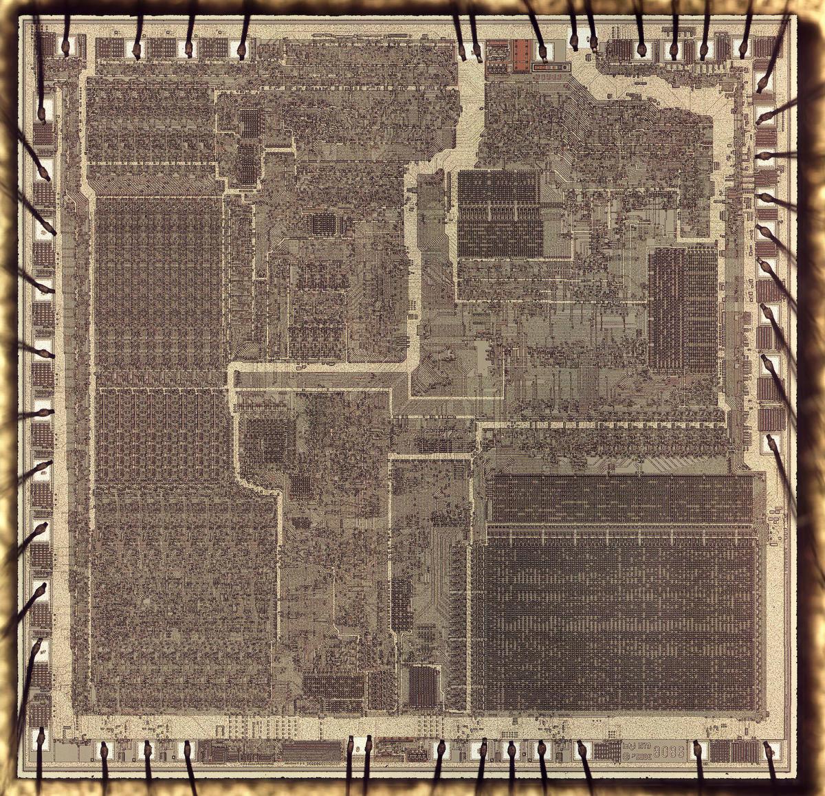
I quickly noticed, however, that this wasn't an 8086 processor but something entirely different! For comparison, look at my die photo of a genuine 8086 below. As you can see, the chips are entirely different and the 8086 is much more complex. Someone had taken a random 40-pin chip and relabeled it as an Intel 8086 processor. The genuine 8086 has various functional blocks visible: the 16-bit registers and ALU on the left, the large microcode ROM in the lower right, and various other blocks of circuitry throughout the chip. (The genuine chip also has a tiny Intel copyright and the 8086 part number in the lower right. Click the image to magnify.) The fake chip above, on the other hand, is an irregular grid of horizontal and vertical wiring, with thicker horizontal and vertical lines for power.

Die photo of a genuine 8086 chip.

Die photo of a genuine 8086 chip.

The ULA or Uncommitted Logic Array

If the chip isn't an 8086, what is it? I believe the fake chip is an Uncommitted Logic Array, a type of gate array. A gate array is a way of making semi-custom integrated circuits without the expense of a fully-custom design. The idea behind a gate array is that the silicon die has a standard array of transistors that can be wired up to create the desired logic functions. This wiring is done in the chip's metal layers, which are designed for the customer's requirements.2 Although a gate array doesn't provide the flexibility of a fully-custom design, it was considerably cheaper and faster to design.

Ferranti invented the ULA in 1972, claiming that it was the first "to turn the logic array concept into a practical proposition." A ULA allowed a single LSI chip to replace hundreds or even thousands of gates that otherwise would be implemented in a board full of 7400-series TTL chips. The most well-known users of a ULA are the popular Sinclair ZX 81 and ZX Spectrum home computers.3

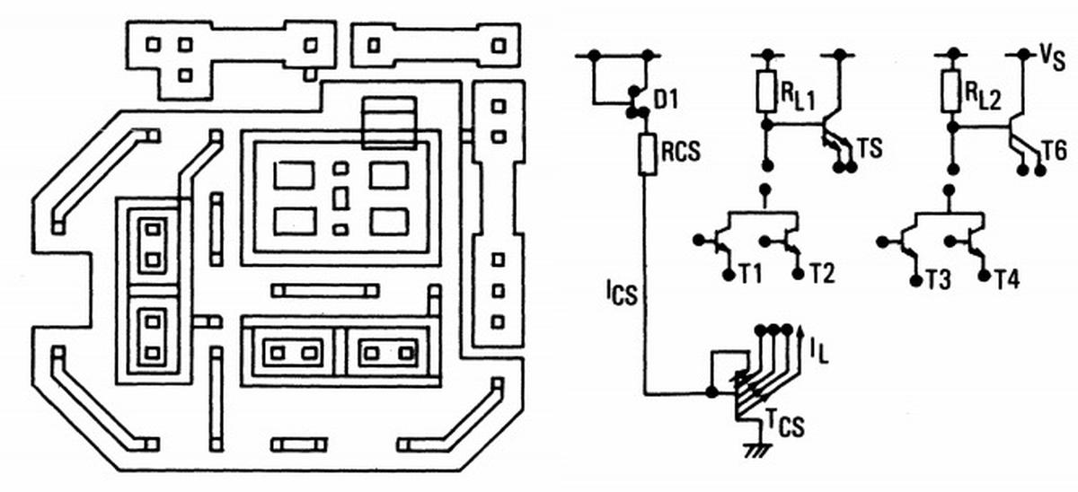
A ULA was based on a matrix of identical cells that were wired to form the logic gates. Around the edges of the chip, standardized peripheral cells provided the desired I/O capabilities. The diagram below shows a typical cell in the matrix. The cell contains multiple transistors and resistors, which are mostly unconnected by default. The ULA is customized by creating connections between the components to build a set of logic gates.

Layout and schematic of a ULA matrix cell. From Ferranti Quick Reference Guide.

Layout and schematic of a ULA matrix cell. From Ferranti Quick Reference Guide.

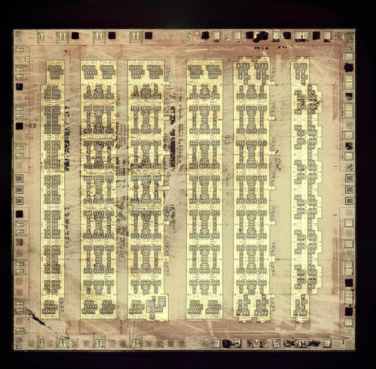
The photo below shows the fake chip with the metal layers removed, revealing the transistor array underneath. Each small green/yellow rectangle is a transistor; there are nearly 1000 of them. Note the repeated pattern of cells in the matrix,1 as well as the different peripheral cells around the outside. The density of transistors is fairly low; the chip has empty columns to provide room to route the metal layer.

Die photo of the fake 8086 showing the underlying silicon. The metal layers were removed for this photo.

Die photo of the fake 8086 showing the underlying silicon. The metal layers were removed for this photo.

The fake chip uses bipolar transistors,4 completely different from the NMOS transistors in the 8086 processor. The closeup below shows transistors (the striped rectangles) and the two layers of metal wiring connecting them. (The genuine 8086 only has one metal layer, so the fake chip is probably more recent, from the 1980s.)

A closeup of the fake chip showing transistors.

A closeup of the fake chip showing transistors.

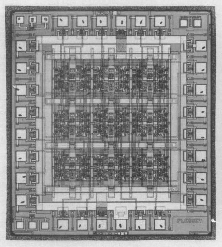
There is no manufacturer printed on the die of the fake chip. The matrix cells don't look like the Ferranti cells. The photo below shows a ULA built by Plessey, another ULA manufacturer. That die has a smaller transistor matrix than my chip, but the overall structure is roughly similar, so Plessey might be the manufacturer.

A Plessey ULA die. From "Computer Aided Design and New Manufacturing Methods for Electronic Materials", 1985.

A Plessey ULA die. From "Computer Aided Design and New Manufacturing Methods for Electronic Materials", 1985.

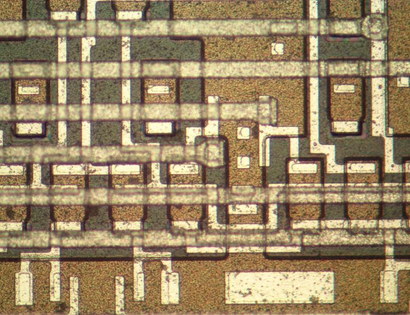
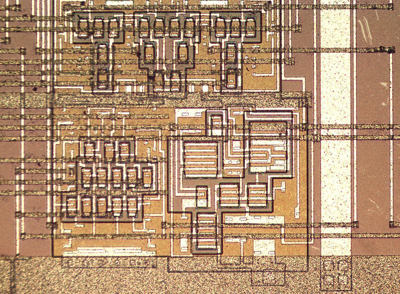
The photo below shows another detail of the fake chip. Matrix cells are at the top. The peripheral cell below has much larger transistors for I/O. (There are also resistors in the brownish regions, but they aren't really visible.) The upper metal layer consists of horizontal wiring, while the lower metal layer is mostly vertical. The thick metal line at the right is for power (or perhaps ground) and is connected to a horizontal power distribution trace at the bottom.

Detail of the fake 8086, showing transistors, resistors, and metal wiring.

Detail of the fake 8086, showing transistors, resistors, and metal wiring.

To summarize, the position of the transistors and resistors in the ULA is fixed. This allows the same underlying silicon wafers to be manufactured for all the customers, keeping volume high and costs low. But by customizing the metal wiring layers, the ULA can be completed to fulfill the logic functions each customer needs.

Conclusions

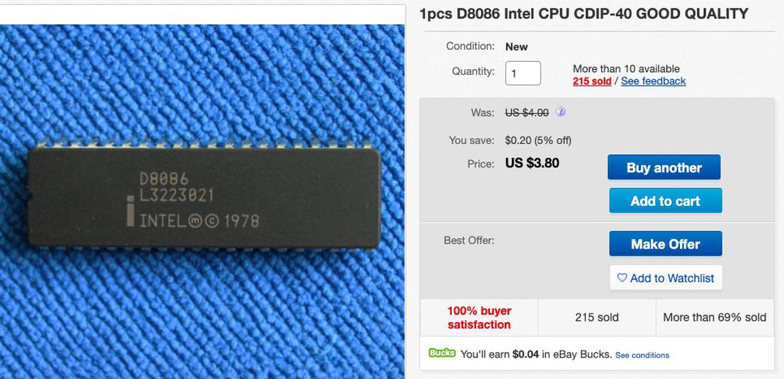
Why would someone go to all the work of relabeling a $3.80 chip? I guess someone had a stack of old custom ICs with no value. By re-labeling them, they could at least get something for them. It hardly seems worth the effort, but I guess they make up for it in volume. The seller has sold over 215 of these 8086's, although I don't know if they were all fake or if I was unlucky. In any case, the seller gave me a prompt refund.

The fake 8086 for sale on eBay.

The fake 8086 for sale on eBay.

The seller's feedback (below) shows a lot of complaints about fake chips. Even so, the seller's feedback is 99.2% positive, so I suspect that there are just a few fake chips mixed in with many types of real chips. It's also possible that most vintage 8086s are purchased by IC collectors who never test the chip.

Feedback on the seller.

Feedback on the seller.

I've been asked if this chip would actually work as an 8086. Sometimes counterfeiters sell a lower-quality chip in place of the real thing, such as the fake expensive op amps found by Zeptobars. But other times the fake chip is unrelated, such as the vintage bipolar RAM chips that I determined was a Touch-Tone dialer. Since an 8086 has 29,000 MOS transistors but the fake chip has under 1000 bipolar transistors, it's clear that this chip won't function as an 8086.

The moral is to always be careful when you're buying chips, since you never know what you might find. Semiconductor counterfeiting is a big business and I've encountered just a tiny piece of it. I plan to write more about reverse-engineering the (real) 8086, so follow me on Twitter at @kenshirriff for updates. I also have an RSS feed.

Notes and references

  1. I think the fake chip has a matrix of 8×12 cells, with each of the large "IXI" patterns composed of four cells. 

  2. At first, a ULA was designed by hand by an engineer drawing the interconnects on paper, but by the 1980s, CAD software automated most of the design and testing. The CAD station below is pretty wild.

    CAD system for designing ULAs at Plessey. From "Computer Aided Design and New Manufacturing Methods for Electronic Materials", 1985.

    CAD system for designing ULAs at Plessey. From "Computer Aided Design and New Manufacturing Methods for Electronic Materials", 1985.


  3. The book The ZX Spectrum ULA: How to design a microcomputer discusses Ferranti ULAs in detail along with a complete explanation of the ULA in the ZX Spectrum. 

  4. Early ULAs used bipolar transistors, with CMOS circuitry introduced later. Different logic families were supported, depending on the needs of the application. Ferranti's ULAs had three types of matrix cells: RTL (resistor-transistor logic), CML (current-mode logic), and buffered current-mode logic. Other ULAs supported fast ECL (emitter-coupled logic) or standard TTL (transistor-transistor logic). 

How the 8086 processor handles power and clock internally

One under-appreciated characteristic of early microprocessors is the difficulty of distributing power inside the integrated circuit. While a modern processor might have 15 layers of metal wiring, chips from the 1970s such as the 8086 had just a single layer of metal, making routing a challenge. Similarly, clock signals must be delivered to all parts of the chip to keep it in synchronization.

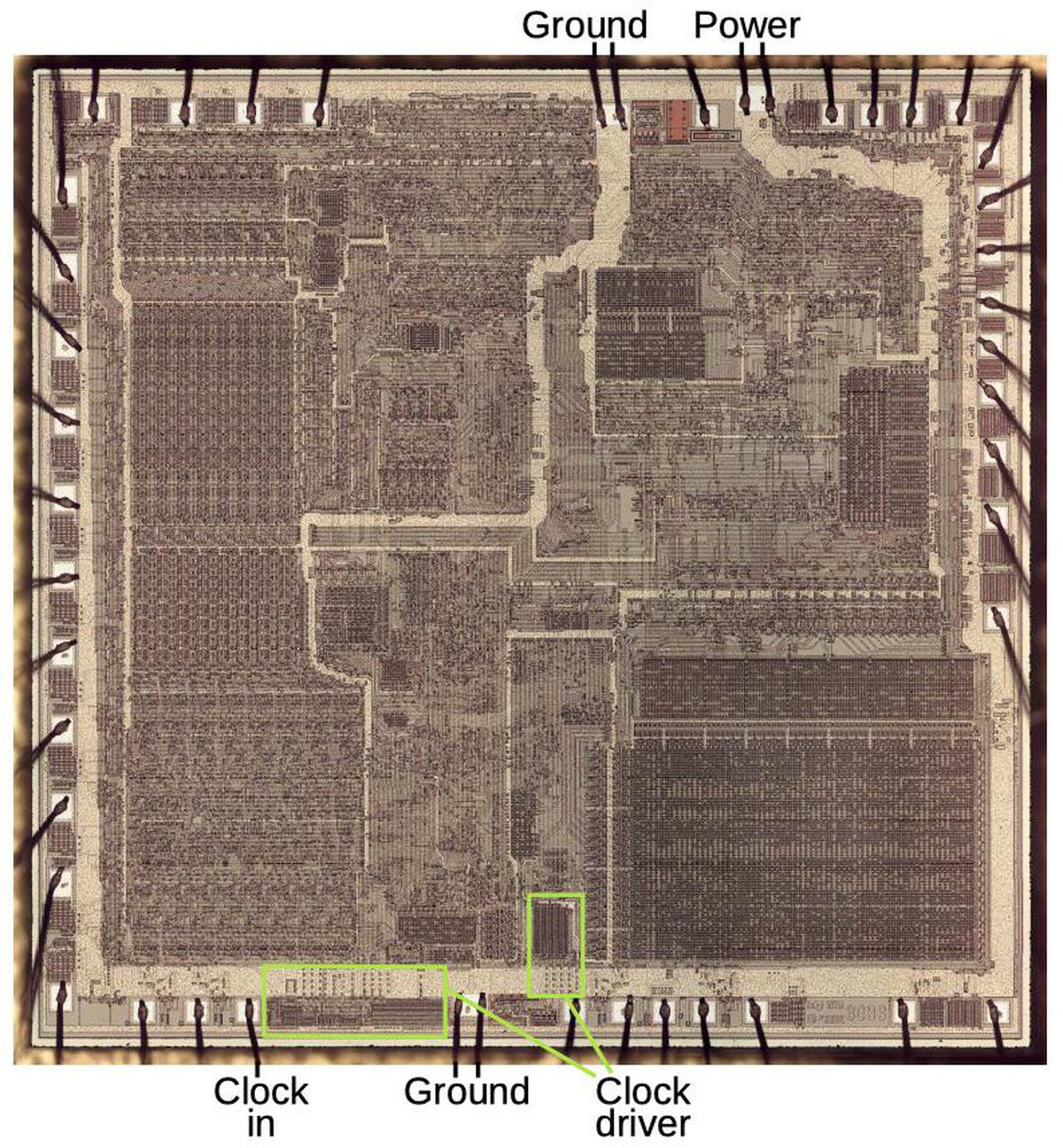
The photo below shows the 8086's die under a microscope. The metal layer on top of the chip is visible, with the silicon substrate and polysilicon wiring hidden underneath. Around the outside of the die, tiny bond wires connect pads on the die to the external pins. The 8086 has a power pad at the top and ground pads at the top and bottom. Each power and ground pad has two bond wires connected to support twice the current. You can see the wide metal traces from the power and ground pads; these distribute power throughout the chip.

Die photo of the 8086 showing power connection (top) and ground connections (top, bottom). The clock circuitry is at the bottom.

Die photo of the 8086 showing power connection (top) and ground connections (top, bottom). The clock circuitry is at the bottom.

Timing in the 8086 is controlled by two internal clock signals. An external oscillator provides a clock signal to the 8086 through the clock input pad at the bottom. The on-chip clock driver circuitry generates two high-current clock signals from this external clock. Note that the clock driver takes up a not-insignificant part of the chip.

In this blog post, I'll discuss how the 8086 routes power and clock signals through the chip, and how the clock driver circuit generates the necessary clock pulses.

Power distribution

The 8086 is constructed with three layers that can be used for wiring. The metal layer on top is best for wiring, since metal has low resistance. Underneath the metal is a layer of polysilicon wiring, made from a special type of silicon. Polysilicon has higher resistance than metal, but can still be used to transmit signals across the chip. The silicon substrate is where the transistors are formed. Silicon has relatively high resistance, so it is only used for short-distance connections, such as inside a gate.

Power routing in a chip like the 8086 creates a topological puzzle of sorts: The metal layer is the only practical layer for routing power and ground, due to its low resistance. Power and ground must be provided to nearly every gate in the chip.1 And since the chip has a single metal layer, power and ground can't cross.

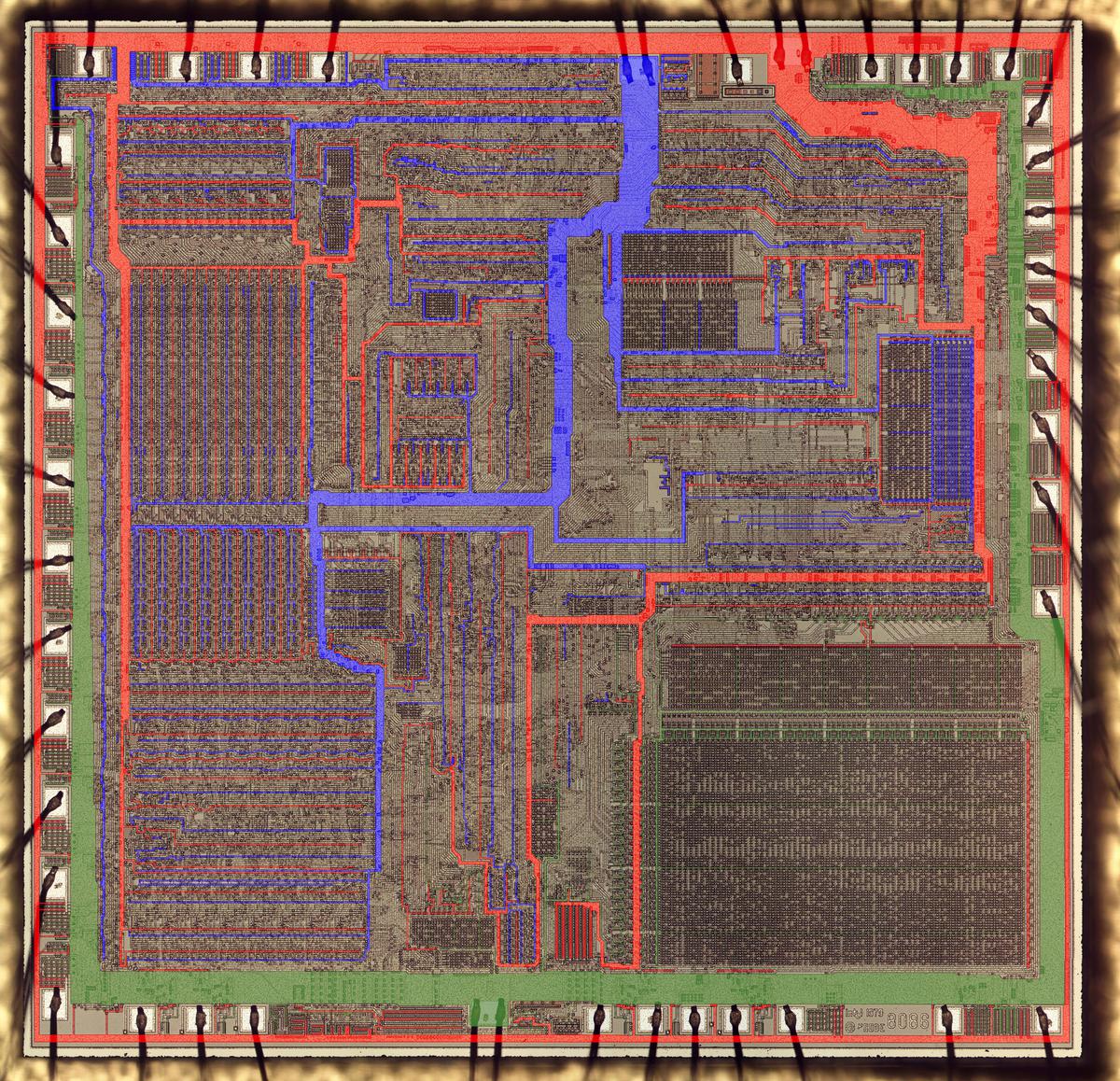
The diagram below highlights these metal wiring networks in the 8086. Power, connected to the power pin at the top, is shown in red, traveling throughout the chip. A major branch flows down and to the right from the power pin, then splitting into multiple paths. Power also travels around the border of the entire chip, supplying the I/O pins.

Power (red) and ground (blue, green) on the metal layer.

Power (red) and ground (blue, green) on the metal layer.

There are two ground pins. The wiring in blue is connected to the upper ground pin, while the wiring in green is connected to the lower ground pin. The blue ground wiring has a large branch downwards through the center of the chip, branching in complex directions. The green ground wiring flows along the bottom, left, and right sides of the chip, supporting the I/O pins, as well as connected to the microcode ROM in the lower right.

The power wires get thinner from their source to their final destination as they branch or deliver power along the way and the current diminishes. This is visible in the ground wire to the address / data pins, below. At the left, the ground wire below the pins is very wide, but it tapers off to the right. In other words, at the left, the wire must handle current for all the pins, but at the right the wire is supporting just the remaining pin.

The ground connection to the Address/Data pins gets progressively thinner. (Left side of chip, rotated 90°)

The ground connection to the Address/Data pins gets progressively thinner. (Left side of chip, rotated 90°)

The metal layer is used for many signals besides power and ground; it is the best layer for delivering signals due to its low resistance. However, the extensive power and ground wiring constrains the other uses of the metal layer. To avoid intersections, most of the metal signal lines run parallel to the power lines; the polysilicon layer underneath is used to run perpendicular signals. But what happens if metal wires need to cross a power or ground line? The solution is to use a "crossunder", where the signal goes down to the polysilicon layer and crosses under the power line, popping back up on the other side,3 as shown below.

Signals in the metal layer crossing under the power line by using polysilicon crossunders.

Signals in the metal layer crossing under the power line by using polysilicon crossunders.

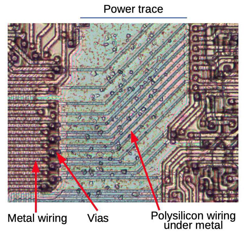
While power and ground are almost entirely routed in the metal layer, there are a few places where this breaks down and a crossunder is used for power. This typically happens near the end of the line, where the current is small. One example is shown below, where ground passes through two polysilicon crossunders. To reduce the resistance, these crossunders are much wider than the crossunders for signals and also use the silicon and polysilicon layers together. The small circles are connections (called vias) between the metal layer and the polysilicon layer.

Composite photo showing polysilicon crossunders for ground that pass under signal lines.

Composite photo showing polysilicon crossunders for ground that pass under signal lines.

The silicon layer plays a minor part in routing power. In particular, many gates are stretched out to reach the power and ground on either side. The photo below shows some gates in the 8086. Note the large doped silicon regions (white) that extend to reach the power and ground lines. Only a small part of this silicon is used for transistors, while the rest looks like wasted space. However, these empty silicon regions connect the gate to the metal power and ground wires. Since silicon has relatively high resistance, wide regions are used for these connections, and over short distances.

The doped silicon forming gates can be extended to reach the power and ground lines. The metal layer was removed for this photo so the power and ground lines are illustrated.

The doped silicon forming gates can be extended to reach the power and ground lines. The metal layer was removed for this photo so the power and ground lines are illustrated.

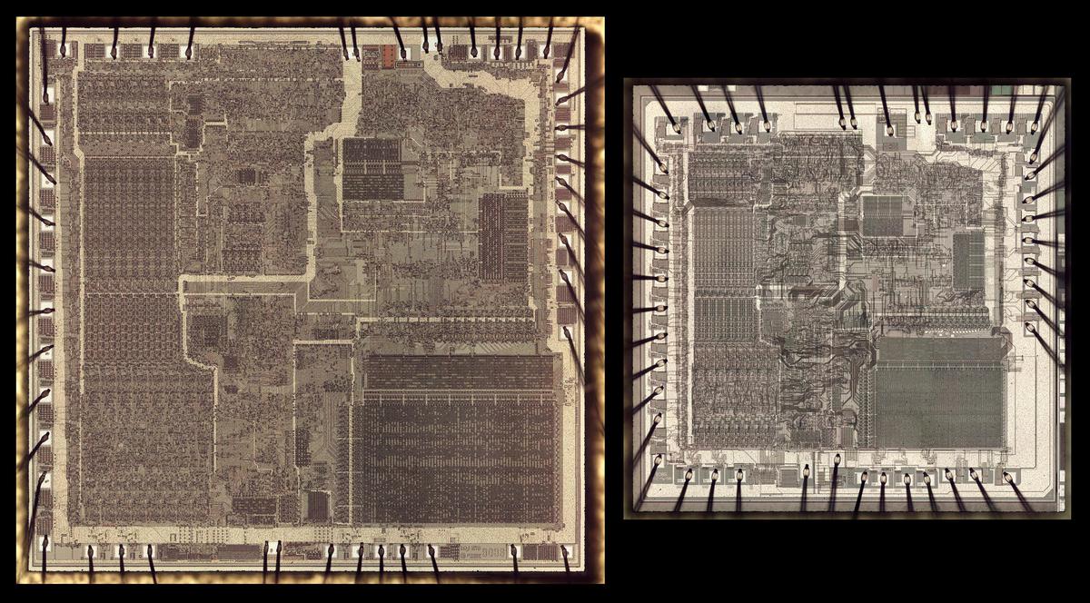
Other power routing issues arose as the 8086 was revised and became physically smaller. As manufacturing technology improved, Intel performed "die shrinks", keeping the same circuitry but scaling it down uniformly to produce a smaller die. Unfortunately, shrinking the power lines reduces the current they can handle. The solution was beef up the power lines around the edge of the chip, while allowing the internal circuitry and wiring to shrink. This can be seen in the photo below; the lower-right corner of the smaller 8086 has much more power wiring, for instance. (I wrote more about the 8086 die shrink here.)

Two versions of the 8086 die, at the same scale. The die on the right is a later version of the 8086, reduced in size.

Two versions of the 8086 die, at the same scale. The die on the right is a later version of the 8086, reduced in size.

The processor clock

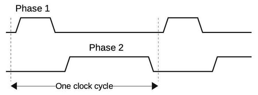
Almost all computers use a clock signal to control the timing of the processor.4 Like many microprocessors, the 8086 uses a two-phase clock internally.5 In a two-phase clock, there are two clock signals: when the first clock is high, the second is low, and vice versa, as shown below. One set of circuitry is enabled by the first clock, while a second set of circuitry is enabled by the second clock. The 8086's circuitry requires that the two clock phases are non-overlapping —there is a gap after one goes low before the other goes high—and asymmetrical.6

A two-phase clock consists of two clock signals with opposite polarity.

A two-phase clock consists of two clock signals with opposite polarity.

In modern processors, clock routing is complex because the clock signals must reach all parts of the chip at the same time. Modern processors use a hierarchy of clock paths, balancing the time along each path, and often provide separate buffering for each path. In comparison, the 8086's clock routing is straightforward because its 5 to 10 MHz clock7 is orders of magnitude slower than modern processors. At these comparatively low speeds, the length of the path doesn't make much difference, so the 8086's clock signals can meander around the chip.

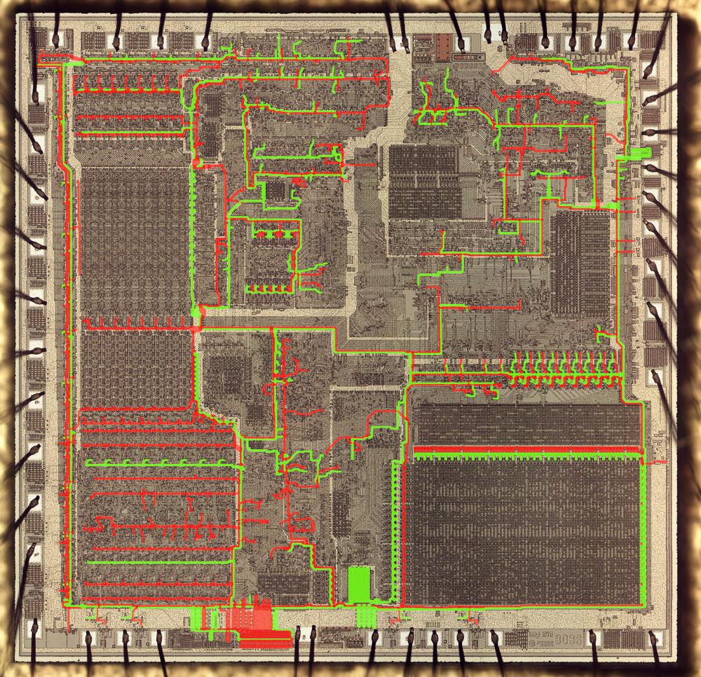
Clock routing in the 8086. Green is clock while red is the opposite phase clock.

Clock routing in the 8086. Green is clock while red is the opposite phase clock.

The diagram above shows the 8086's clock routing. Phase 1 is in green and phase 2 is in red. At the bottom of the chip, the circuitry that generates the clocks appears as large blobs. From there, the clock signals branch wind around the chip. For the most part, the two clock phases are routed parallel to each other, unlike power and ground, which form opposing branches.

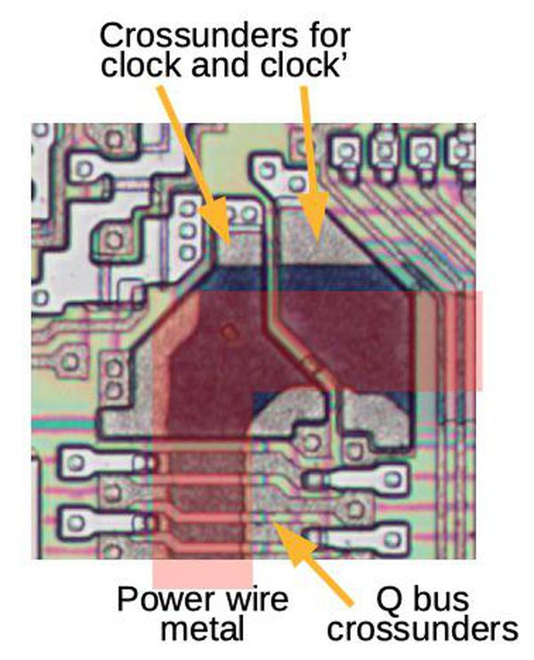
Because the clock signals go to all parts of the chip, they require much more current than typical signals and are routed in the metal layer for the most part. When the clock signals must cross the power lines, they use large crossunders as shown below. Note that the irregularly-shaped clock crossunders are much larger than the crossunders for other signals, such as the Q bus below.

The clock has large crossunders to cross the power wire. The Q bus (which transfers instructions from the instruction queue to the decoder) has much smaller crossunders.

The clock has large crossunders to cross the power wire. The Q bus (which transfers instructions from the instruction queue to the decoder) has much smaller crossunders.

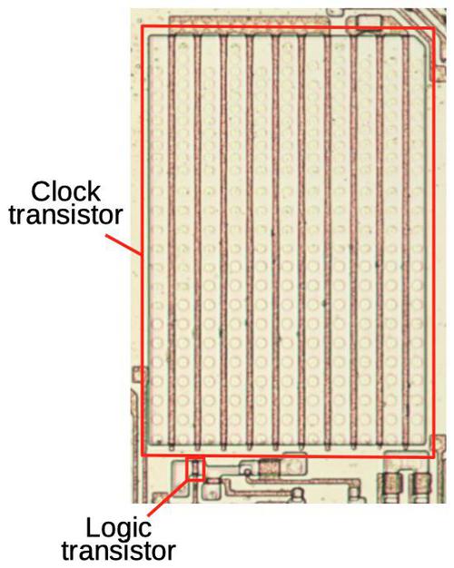
To provide the high-current clock signals, the clock signals have special driver circuitry built from large transistors. The photo below compares one of these driver transistors to a typical logic transistor. The driver transistor is about 300 times as large, so it can provide about 300 times the current. This transistor is constructed as 10 transistors in parallel; the 10 vertical polysilicon lines form the 10 gates. Each clock signal is driven by a pair of large transistors, one to pull the signal high and one to pull the signal low.

A large transistor in the clock driver compared to a neighboring logic transistor.

A large transistor in the clock driver compared to a neighboring logic transistor.

The photo below shows the clock driver circuitry. This circuit splits the external clock signal into two phases, makes the phases non-overlapping, and amplifies them. At the left, the pink square is the pad for the externally-supplied clock. The signal passes through a series of transistors, ending with the large driver transistors at the right for the clock signal. The brownish wiring is the polysilicon that forms the gates. Many transistors have zig-zagging gates to fit a larger transistor into the available space.

The clock driver circuitry on the die. The metal has been removed, revealing the large transistors in the circuit. The clock input pin is the purple square on the left.

The clock driver circuitry on the die. The metal has been removed, revealing the large transistors in the circuit. The clock input pin is the purple square on the left.

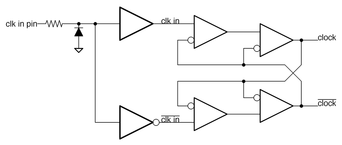
The schematic below shows the driver circuitry, slightly simplified. The triangles indicate high-current drivers, built from two or three transistors; an inverting input (indicated by a bubble) pulls the output low. At the left, the clock input pin has a small resistor and a diode to provide some protection (like the other input pins). Next, the clock is split into an uninverted phase (top) and an inverted phase (bottom).

Simplified schematic of the clock driver circuitry in the 8086.

Simplified schematic of the clock driver circuitry in the 8086.

The additional circuitry keeps the clocks from overlapping: when one clock is high, it forces the other side low, through the inverted inputs. To see how this works, let's start with the clk in pin high, so clk in and clock are high while clk in and clock are low. Now, suppose the clk in pin input goes low, causing clk in to go low and clk in to go high. However, the output clock can't go high until clock goes low, due to the negative inputs on the buffers. Once that happens, clk in proceeds through the lower drivers, pulling clock high after two gate delays.8 The point of this is that clock and clock don't switch at the same time; after one goes low, there is a delay before the other goes high. This generates the desired non-overlapping clock signals.

Conclusions

The 8086 uses some interesting routing for power, but modern processors operate at a whole different level. While the 8086 required 350 milliamps of current, a modern processor might require over a hundred amps. The 8086 used 3 of its 40 pins for power and ground, compared to a modern Intel Core i5 processor with 128 power pins and 377 ground pins (out of 1151 pins). Although the numerous metal layers in modern chips solved the 8086's routing issues, modern chips have new complications such as multiple power domains that allow unused parts of the chip to be powered down.

Clock routing is much harder on modern processors since at multi-gigahertz speeds, even an extra millimeter of path can affect the clock. To deal with this, modern processors use techniques such as H-trees or grids to distribute the clock, rather than the 8086's meandering paths. While the 8086 has a simple circuit to generate the two-phase clock, modern processors often use a phase-locked loop (PLL) to synthesize the clock and use multiple circuits scattered across the chip to generate and control clock signals.

Even though the 8086 is much simpler than modern processors, it contains a lot of interesting circuitry. I plan to reverse-engineer more of the 8086, so follow me on Twitter at @kenshirriff for updates. I also have an RSS feed.

Notes and references

  1. Power and ground must be provided to almost every gate in the chip since a standard NMOS gate requires ground for its pull-down network and power for its pull-up resistor. There are a few exceptions, though. The 8086 uses some dynamic logic gates, especially in the ALU for speed. These gates are pulled high by the clock, so they don't need a direct power connection. The 8086 also uses some pass-transistor XOR gates, which are pulled low by the inputs, so they don't need ground.

    The microcode ROM forms a large region with no power connections, just ground. This is because each row in the ROM is implemented as a very large NOR gate with the power pull-up on the right-hand edge. Thus, the ROM gates all have power and ground, even though it looks like the ROM lacks power connections. 

  2. Integrated circuits often have power and ground on opposite corners or opposite sides of the chip. This placement makes it easier to construct the non-intersecting power and ground networks in the chips. The 8086 is slightly unusual to have power and ground on diagonally-opposite pins, but then a second ground pin close to the power pin. The solution is to have tree-like branching networks for power and ground. These networks are interdigitated, meshed like fingers to reach all parts of the chip.2 

  3. Crossunders are used for many wire crossings, not just power, but power wiring is a key contributor. Typically, metal wiring is used for signals in one direction, while polysilicon wiring is used for signals in the perpendicular direction. (These directions vary in different parts of the chip, depending on the predominant direction for signals.) Thus, signals for the most part can travel unimpeded. Even so, signals often bounce from layer to layer to make the routing work. 

  4. While almost all computers are synchronous and operate with a clock, the IAS machine architecture (popular in the 1950s) was asynchronous, operating without a clock. Instead, each circuit would send a pulse to the next when it was done, triggering the next step. Many early computers of the 1950s were based on the IAS machine architecture, including CYCLONE, ILLIAC, JOHNNIAC, MANIAC, SEAC, and the IBM 701. Research into asynchronous computing continues (link, link), but synchronous designs are dominant. 

  5. Among other things, processors use the clock to prevent unwanted feedback in the circuitry. For instance, consider a program counter with a circuit to increment it and feed the result back to the program counter. You don't want the new value to get repeatedly incremented.

    One approach is to use edge-sensitive circuits (flip flops) that will update that value in the program counter at the moment the clock goes high. Thus, there will be a single update as desired. However, with a two-phase clock, the circuit can be built from level-sensitive latches, which are much simpler than edge-sensitive flip flops. The idea is that when the first clock is high, the first half of the circuit receives input and does its logic calculations When the second clock is high, the second half of the circuit receives input from the first half and does any necessary calculations, while the first half is blocked. The point is that only half of the circuitry can update at any time, preventing uncontrolled feedback. 

  6. The 8086 has strict requirements on its input clock, which must be high for 1/3 of the time. The clock signal into the 8086 was typically produced by an 8284 chip and a quartz crystal. This chip divided its input clock by 3 to generate the 33% duty cycle clock required by the 8086.  

  7. Because the 8086 used dynamic logic, it also had a minimum clock speed of 2 MHz. If the clock ran slower than this, there was a risk of charges leaking away before they were refreshed, causing failures. The minimum clock speed was inconvenient for debugging, since you couldn't slow down or stop the clock. 

  8. This is a somewhat handwaving description of the clock driver circuit. In particular, I'm not sure what happens when one transistor is pulling a signal high and another is pulling the same signal low. An accurate simulation would depend on the relative sizes of the two transistors.