How "special register groups" invaded computer dictionaries for decades

Half a century ago, the puzzling phrase "special register groups" started showing up in definitions of "CPU", and it is still there. In this blog post, I uncover how special register groups went from an obscure feature in the Honeywell 800 mainframe to appearing in the Washington Post.

While researching old computers, I found a strange definition of "Central Processing Unit" that keeps appearing in different sources. From a book reprinted in 2017:1

"Central Processor Unit (CPU)—Part of a computer system which contains the main storage, arithmetic unit and special register groups. It performs arithmetic operations, controls instruction processing and provides timing signals."

"Central Processor Unit (CPU)—Part of a computer system which contains the main storage, arithmetic unit and special register groups. It performs arithmetic operations, controls instruction processing and provides timing signals."

At first glance, this definition seems okay, but a few moments thought reveals some problems. Storage is not part of the CPU. But more puzzling, what are special register groups? A CPU has registers, but "special register groups" is not a normal phrase.

It turns out that this definition has been used extensively for over half a century, even though it doesn't make sense, copied and modified from one source to another. Special register groups were a feature in the Honeywell 800 mainframe computer, introduced in 1959. Although this computer is long-forgotten2, its impact inexplicably remains in many glossaries. The Honeywell 800 allowed eight programs to run on a single processor, switching between programs after every instruction.3 To support this, each program had a "special register group" in hardware, its own separate group of 32 registers (program counter, general-purpose registers, index registers, etc.).

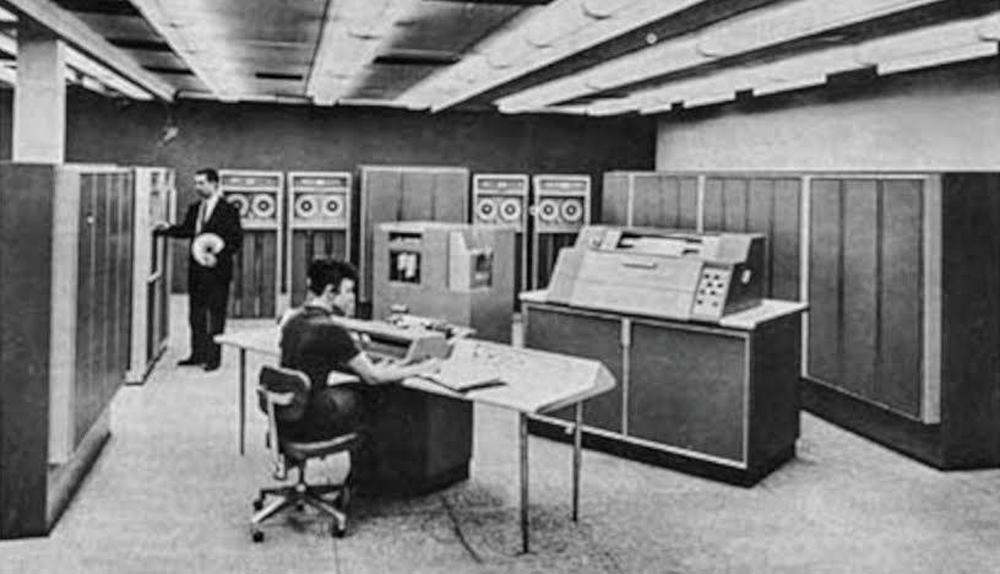
Honeywell 800 computer. The Central Processing Unit (containing special register groups) is in cabinets 6 feet high and 18 feet wide along the wall. The card reader and printer are in the center of the room. A typical system rented for $25,000 a month. Photo from BRL report, 1961 courtesy of Ed Thelen.

Honeywell 800 computer. The Central Processing Unit (containing special register groups) is in cabinets 6 feet high and 18 feet wide along the wall. The card reader and printer are in the center of the room. A typical system rented for $25,000 a month. Photo from BRL report, 1961 courtesy of Ed Thelen.

Another important thing to note about that era is the central processing unit was a large physical box, also known as the "main frame". (A mainframe was not a type of computer yet.) Thus, given the characteristics of the Honeywell 800, the definition of CPU in Honeywell's glossary4 made total sense.5 Unfortunately, this definition doesn't make sense when used for computers in general, since they lack special register groups.

Honeywell's definition of main frame: "FRAME, MAIN, (I) the central processor of the computer
system. It contains the main storage, arithmetic unit and
special register groups. Synonymous with (CPU) and
(central processing unit). (2) All that portion of a computer exclusive of the input, output, peripheral and in some
instances, storage units."

Honeywell's definition of main frame: "FRAME, MAIN, (I) the central processor of the computer system. It contains the main storage, arithmetic unit and special register groups. Synonymous with (CPU) and (central processing unit). (2) All that portion of a computer exclusive of the input, output, peripheral and in some instances, storage units."

This definition apparently started with the US Department of Agriculture's Glossary of ADP Terminology (1960): "MAIN FRAME - The central processor of the computer system. It contains the main memory, arithmetic unit and special register groups". The definition then spread through the government. The Bureau of the Budget published the Automatic Data Processing Glossary in 1962 "for use as an authoritative reference by all officials and employees of the executive branch of the Government" with the definition below. The Air Force's 1966 Guide for Auditing Automatic Data Processing Systems used a similar definition as did the 1966 Navy Training Course for Machine Accountant and 1968 Air Force manual Communications-Electronics Terminology.

Bureau of the Budget's 1962 definition: "frame, main, (1) the central processor of the computer system. It contains the main storage, arithmetic unit and special register groups. Synonymous with CPU and central processing unit. (2) All that portion of a computer exclusive of the input, output, peripheral and in some instances, storage units."

Bureau of the Budget's 1962 definition: "frame, main, (1) the central processor of the computer system. It contains the main storage, arithmetic unit and special register groups. Synonymous with CPU and central processing unit. (2) All that portion of a computer exclusive of the input, output, peripheral and in some instances, storage units."

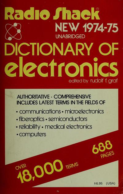
From there, the definition spread to dozens of books and dictionaries. The "special register groups" appeared in numerous computer glossaries such as the Glossary of Computing Terminology (1972), Computer Glossary for Medical and Health Sciences (1973) Computer Glossary for Engineers and Scientists (1973), Radio Shack's Dictionary of Electronics (1968, 1974-1975), and Computer Graphics Glossary (1983)

Radio Shack's New 1974-1975 Dictionary of Electronics contains the definition:
"central processing unit—Also called central processor. Part of a computer system which
contains the main storage, arithmetic unit, and special register groups. Performs arithmetic operations, controls instruction processing, and provides timing signals and other housekeeping operations."

Radio Shack's New 1974-1975 Dictionary of Electronics contains the definition: "central processing unit—Also called central processor. Part of a computer system which contains the main storage, arithmetic unit, and special register groups. Performs arithmetic operations, controls instruction processing, and provides timing signals and other housekeeping operations."

Computer manufacturers should know their systems don't have special register groups, but they still used the definition. For example, Sphere microcomputer (1976), Texas Instruments (1978), Cray (1984), Convergent Technologies (1987), and Tektronix (1989).

This definition persisted into the microcomputer age, even though storage was now clearly not part of the CPU and "special register groups" were decades in the past. A 1983 Beginner's Computer Glossary in MICRO magazine defined "CPU — Central Processing Unit. The central processor of the computer system, which contains the main storage, arithmetic unit, and special register groups." "Special register groups" also showed up in Microcomputer Dictionary (1981), and Understanding Microprocessors (1984),

Definitions with "special register groups" appeared in a dizzying array of books, such as Computer Technology in the Health Sciences (1974), College Typewriting (1975), Research Methods for Recreation and Leisure (1979), EPA's Design Automation Handbook for Automation of Activated Sludge Treatment Plants (1980), Patrick-Turner's Industrial Automation Dictionary (1996), Video Scrambling & Descrambling (1998), US Department of Transportation's Computerized Signal Systems (1979). and Traffic Control System Operations (2000).

In 1981, special register groups reached national newspapers in a Washington Post glossary: "Main-frame—central processor of computer system, containing main storage, arithmetic unit and special register groups." By 2006, even the National Fire Code6 included special register groups: "Computer. A programmable electronic device that contains a central processing unit(s), main storage, an arithmetic unit, and special register groups."

Special register groups are still being taught to the next generation of students. The following quiz question is from a 2017 book that teaches computer organization and programming:7

CPU of a computer system does not contain:
(a) Main storage
(b) Arithmetic unit
(c) Special register group
(d) None of the above

Conclusion

For some reason, a 1960 definition of "central processing unit" included "special register groups", an obscure feature from the Honeywell 800 mainframe. This definition was copied and changed for decades, even though it doesn't make sense. It appears that once something appears in an authoritative glossary, people will reuse it for decades, and obsolete terms may never die out.

"Computer operators working with tape-driven Honeywell 800 mainframe computer."
The operators in this photo from the 1960s are presumably taking advantage of the special register groups unique to the Honeywell 800 and 1800 computers.  Photo from National Library of Medicine.

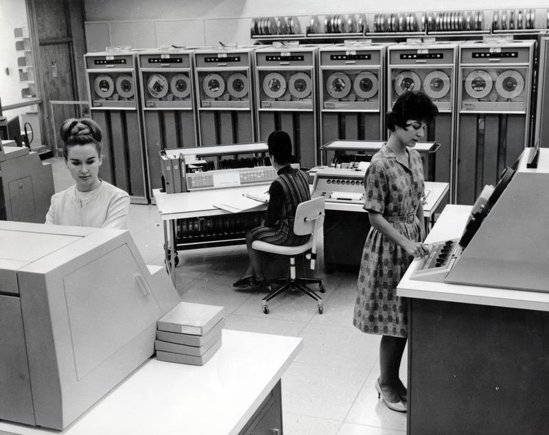
"Computer operators working with tape-driven Honeywell 800 mainframe computer." The operators in this photo from the 1960s are presumably taking advantage of the special register groups unique to the Honeywell 800 and 1800 computers. Photo from National Library of Medicine.

Researching this phrase also shows how the meanings of computer terms shift greatly over time. In 1960, "main frame" and "CPU" were synonyms, but since then they have moved in opposite directions: "mainframe" is now a large computer system, while the "CPU" is usually a processor chip. (I plan to write much more about this.)

I announce my latest blog posts on Twitter, so follow me @kenshirriff for future articles. I also have an RSS feed.

Notes and References

  1. Reference: Reliability Engineering for Nuclear and Other High Technology Systems, CRC Press, 2017, reprint of a book originally published in 1985. 

  2. I happen to be familiar with the Honeywell 800 and 1800 computers because I've been studying the Apollo Guidance Computer extensively. (The Honeywell 1800 was an improved version of the Honeywell 800.) The Honeywell 1800 was used to assemble programs for the Apollo Guidance Computer using an assembler called YUL

  3. The Honeywell 800's technique of switching programs on every instruction is rather unusual. Typical multi-tasking systems let a program run for several milliseconds before switching to another program to reduce the overhead of switching between programs. The Honeywell 800 Programmers Reference Manual explains the use of special register groups for multiprogramming. 

  4. Honeywell's Glossary of Data Processing and Communications Terms was published 1964-1966. Definitions in that book are largely based on the Bureau of the Budget's Automatic Data Processing Glossary. 

  5. The Oxford English Dictionary (1989) quoted the 1964 Honeywell definition. 

  6. Reference: NFPA's Illustrated Dictionary of Fire Service Terms, published by the National Fire Protection Association in 2006. The National Fire Codes (1995) had a somewhat similar definition, but for the CPU instead of computer: "CPU. Central processing unit of the computer system. The CPU contains the main storage, arithmetic unit, and special register groups." 

  7. Reference: Computer Architecture, 2011, published by Biyani. Page 58 contains the quiz with the CPU question. The question also appears in MCS-012: Computer Organisation and Assembly Language Programming, 2017. 

A visit to the Large Scale Systems Museum

I didn't expect to find two floors filled with vintage computers in a small town outside Pittsburgh. But that's the location of the Large Scale System Museum, housed in a former department store. The ground floor of this private collection concentrates on mainframes and minicomputers from the 1970s to 1990s featuring IBM, Cray, and DEC systems, along with less common computers. Amazingly, most of these vintage systems are working. Upstairs, the museum is filled with vintage home computers from the pre-PC era.

IBM

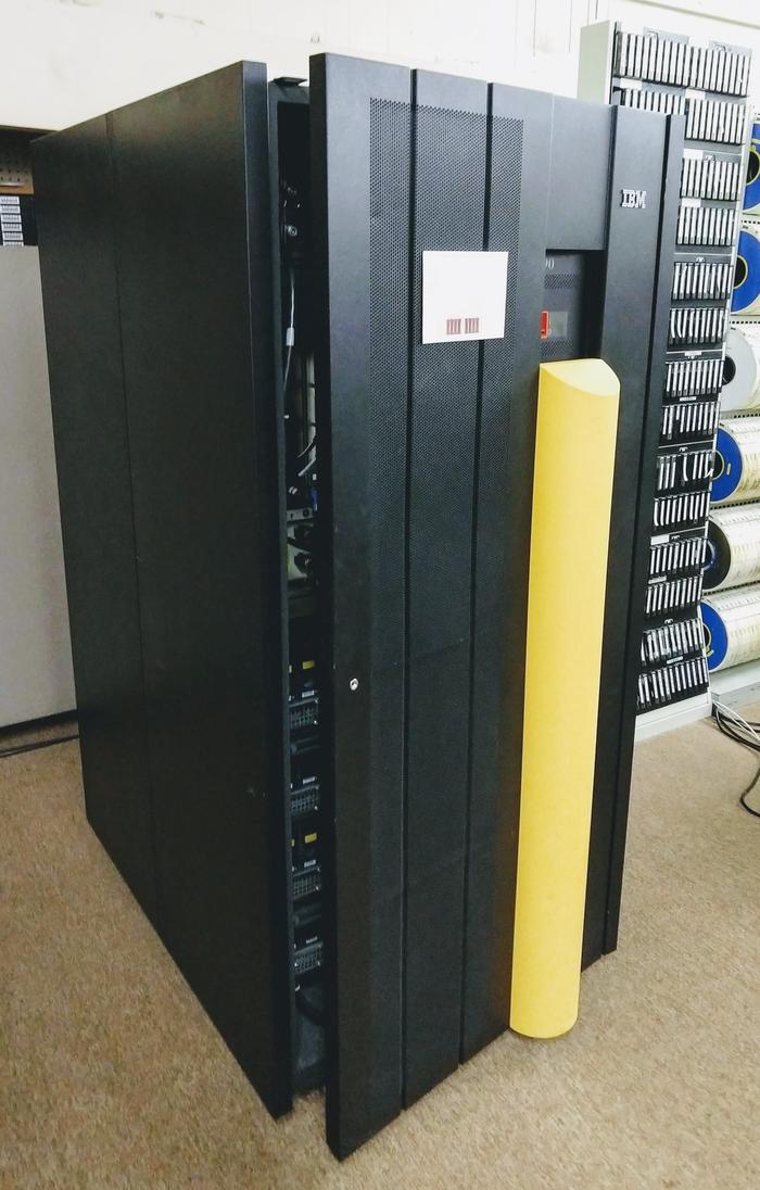
IBM set the standard for the mainframe computer with its introduction of the System/360 in 1964, a line of computers designed to support the full circle (i.e. 360°) of business and scientific applications. The System/360 evolved into the System/370 in the 1970s and the System/390 in the 1990s. Most of these mainframes filled a data center, but the museum has some smaller S/370 and S/390 mainframes designed for offices. The IBM System/370 9375 (1986; below), is described as a "baby mainframe" or "super-mini computer" for engineering or commercial applications.

IBM System/370 9375. The computer itself is in the middle rack. The left rack has a 3490E tape cartridge storage system, while the right rack holds 9335 disk controllers and disk drives (856 MB per drive).

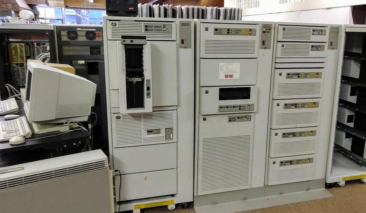
IBM System/370 9375. The computer itself is in the middle rack. The left rack has a 3490E tape cartridge storage system, while the right rack holds 9335 disk controllers and disk drives (856 MB per drive).

The System/390 line is represented by the IBM System/390 Multiprise-2003 (1997; below). This mainframe could not boot up on its own, but required a special desktop PC called the Mainframe Service Element (photo) to initialize the mainframe with microcode and start it up.

This low-end IBM System/390 Multiprise-2003 had 1 GB of memory and supported hundreds of simultaneous database transactions.

This low-end IBM System/390 Multiprise-2003 had 1 GB of memory and supported hundreds of simultaneous database transactions.

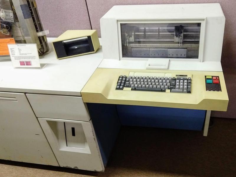
To support smaller customers, IBM also produced minicomputers, which they called "midrange systems". The IBM System/32 (1975; below) is a minicomputer built into a desk, designed for small businesses. IBM's midrange systems evolved into the IBM AS/400 (1992; photo).

This IBM System/32 had 16 KB of memory and 13 MB of disk storage. It leased for $1200 per month.

This IBM System/32 had 16 KB of memory and 13 MB of disk storage. It leased for $1200 per month.

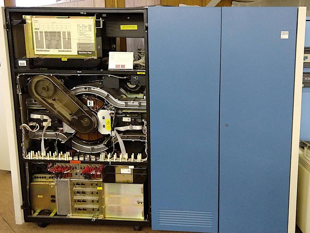
The museum has many disk drives and tape drives. One example is the massive 3380E disk drive (below; 1985), providing 5 gigabytes of storage. It's amazing to think that you can now hold a thousand times as much storage in your hand.

The IBM 3380E disk system stored 5 gigabytes of data. The 14-inch disk platter is in the center, labeled "E".

The IBM 3380E disk system stored 5 gigabytes of data. The 14-inch disk platter is in the center, labeled "E".

Cray

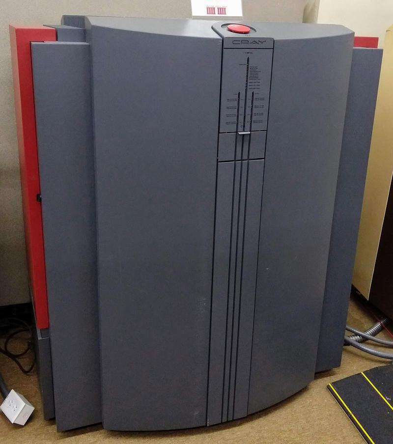
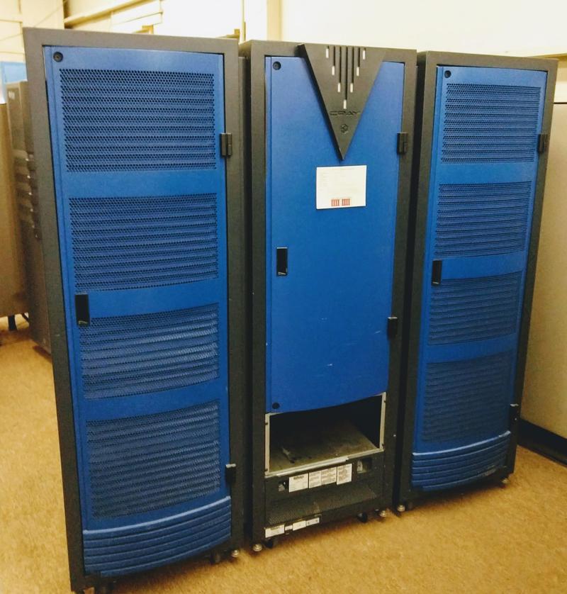
Computer designer Seymour Cray and his company Cray Research were famed for building the world's fastest supercomputers. The museum has several Cray computers from the 1990s. The Cray YMP-EL supercomputer (1992; below) was an "Entry Level" Cray, costing $300,000. It was built from CMOS chips rather than the fast but hot ECL chips in earlier Crays, allowing it to be air-cooled rather than Freon cooled. The museum also has the related, low-end Cray EL-94, packaged in an ugly box (photo; 1992);

The Cray YMP-EL supercomputer.

The Cray YMP-EL supercomputer.

The Cray J90 (1996; below) was a popular low-end Cray, an evolution of the Y-MP EL. This one holds 1 GB of memory and cost $300,000.

Cray J 90 supercomputer.

Cray J 90 supercomputer.

The Cray SV1 (1999; below) followed the J90. It introduced more high-performance features such as a vector cache and multi-streaming. This one has 16 processors and 16 GB of memory, and cost about $1 million.

The Cray SV1 supercomputer.

The Cray SV1 supercomputer.

Digital Equipment Corporation (DEC)

Dave McGuire, curator of the large systems, in front of PDP "Straight 8" minicomputers.

Dave McGuire, curator of the large systems, in front of PDP "Straight 8" minicomputers.

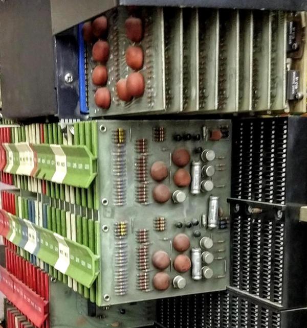
Digital Equipment Corporation was founded in 1957 and became the second-largest computer manufacturer, concentrating on minicomputers. DEC's PDP-8 was a very popular 12-bit minicomputer that essentially created the "minicomputer" category of computers. The first PDP-8 was the Straight-8 (1966; photos above and below), a compact all-transistor computer built from circuit cards plugged into a wire-wrapped backplane.

The "Straight 8" PDP-8 was built from transistorized circuits on small cards.

The "Straight 8" PDP-8 was built from transistorized circuits on small cards.

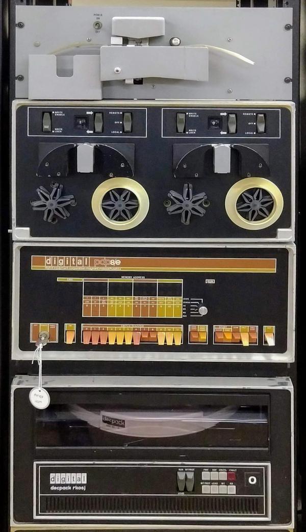
The PDP-8/E (1969; below) used integrated circuits (7400-series TTL) in place of discrete transistors as did the compact and cheaper PDP-8/A (1974; photo).

PDP-8/E minicomputer. The paper tape reader is at the top, above the front panel. An RK05 DECpack is at the bottom, storing 2.4 megabytes on a removable disk pack.

PDP-8/E minicomputer. The paper tape reader is at the top, above the front panel. An RK05 DECpack is at the bottom, storing 2.4 megabytes on a removable disk pack.

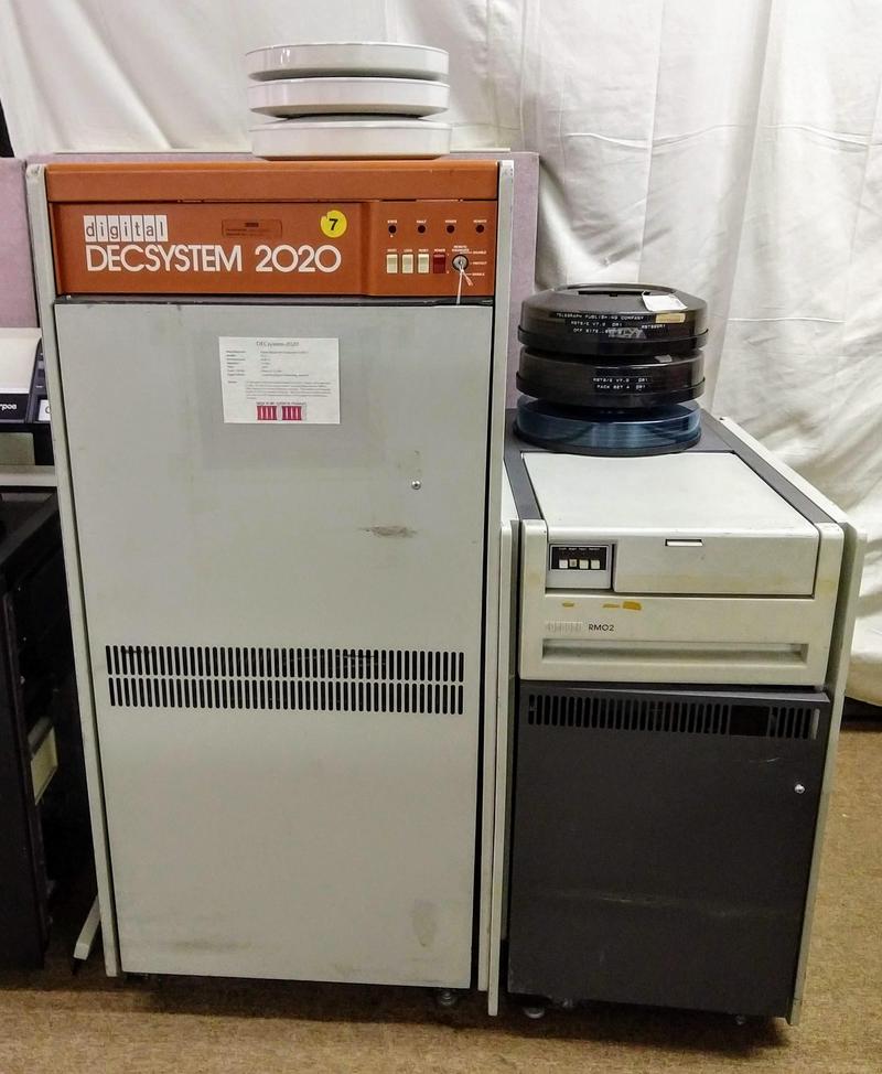
DEC started producing mainframes in 1966 with the PDP-10, a 36-bit computer that popularized time-sharing. The museum has a DECsystem-2020 (1978), the smallest member of the PDP-10 family.

A DECsystem-2020 mainframe next to an RM02 disk drive. The drive's removable disk packs each store 67 megabytes.

A DECsystem-2020 mainframe next to an RM02 disk drive. The drive's removable disk packs each store 67 megabytes.

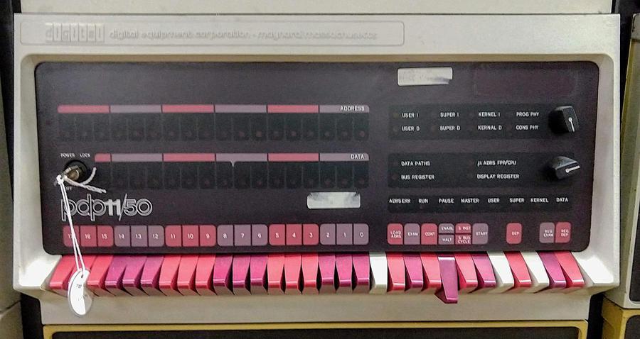
In 1970, DEC introduced the 16-bit PDP-11, which became the most popular minicomputer with about 600,000 sold. The museum has many different PDP-11 models including the PDP-11/05 (1972; photo, console), the fast PDP-11/50 (1972; below, photo), the compact and popular PDP-11/34 (1976; photo), and the PDP-11/44 (1981; photo).

Console of the PDP-11/50 minicomputer.

Console of the PDP-11/50 minicomputer.

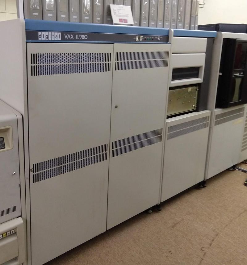
DEC's PDP-11 evolved into the VAX line of 32-bit computers. Larger and more powerful than earlier minicomputers, these systems were known as superminicomputers. The VAX-11/780 (1978; below) was the first member of the VAX family, and was implemented with TTL chips. The museum has a VAX-11/750 (1980) and the cheap single-cabinet VAX-11/730 (1982; photo), the powerful VAX-6000 (1991; photo), and top-of-the-line VAX-7000 (1992; photo). The VAXstation 4000 Model 90 (1991; photo) was a workstation implementing the VAX instruction set.

The VAX 11/780 "superminicomputer".

The VAX 11/780 "superminicomputer".

DEC started struggling in the 1990s as the market shifted to personal computers. DEC was acquired in 1998 by personal computer manufacturer Compaq, which in turn was soon acquired by Hewlett-Packard in 2002.

Other systems

The museum has systems from many other companies such as Varian, Control Data, Wang, Panasonic, Silicon Graphics, Singer, and Tektronix, but I'll just touch on some highlights.

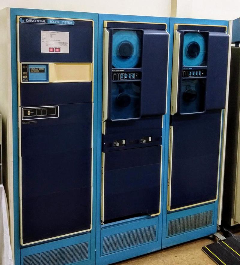
Data General was a major producer of minicomputers, third behind DEC and IBM. The Data General Eclipse was the successor to the popular Data General Nova 16-bit minicomputer. It is represented in the museum by the Eclipse S/280 (1975; below) and Eclipse S/120 (1982; photo). Data General moved into the microcomputer market with the microNOVA (1977; photo), but it wasn't commercially successful.

Data General Eclipse S/280 minicomputer.

Data General Eclipse S/280 minicomputer.

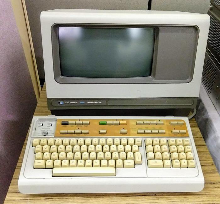
In the late 1970s, Hewlett-Packard was the fourth-largest producer of minicomputers. The HP 2116B minicomputer (1968; photo) was part of the HP 1000 (photo) family of 16-bit minicomputers designed for instrument control and automation. The HP 2645A terminal (below) was part of HP's line of terminals.

HP 2645A terminal

HP 2645A terminal

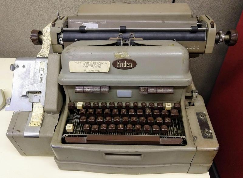
Another interesting terminal is the Friden Flexowriter from the early 1960s (below). It has a paper tape reader and punch on the left. Flexowriters were often used as console terminals for computers.

Friden Flexowriter

Friden Flexowriter

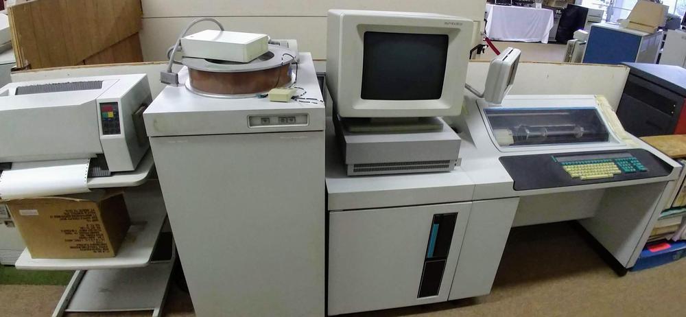
The Burroughs B80 is a multi-user office minicomputer (1978; below). It has as dot-matrix printer above the keyboard. The computer on display was used by a funeral home, and has a paper product list taped above the keyboard with products such as "Tranquility urn", "Open/Close grave", and "Move dirt more than 25 miles".

The Burroughs B80 office minicomputer.

The Burroughs B80 office minicomputer.

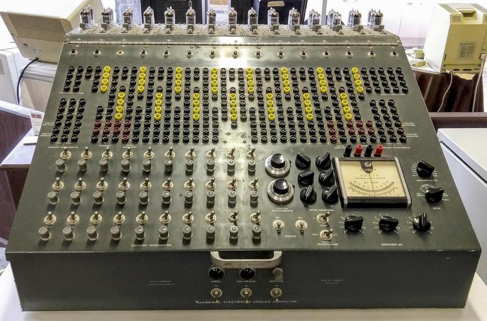
The collection also includes analog computers, such as the Heathkit H-1 (1950s) which used vacuum tube amplifiers and represented values by signals from -100 to 100 volts. It could be programmed to solve differential equations by wiring the patch board. The museum also has a Comdyna GP-6 (photo), a more modern transistorized analog computer from the late 1960s.

A Heathkit H1 analog computer. Vacuum tubes are on top, the plugboard is in the middle, and potentiometer controls are in the front.

A Heathkit H1 analog computer. Vacuum tubes are on top, the plugboard is in the middle, and potentiometer controls are in the front.

Microcomputers in the Large Scale Integration Museum

Upstairs is the "Large Scale Integration Museum", a large collection of microcomputers of the 1970s and 1980s. The collection focuses on microcomputers before to the IBM PC and x86 processors. Since I'm more interested in the larger computers, I'll discuss this collection briefly, but I don't want to downplay its impressive scope.

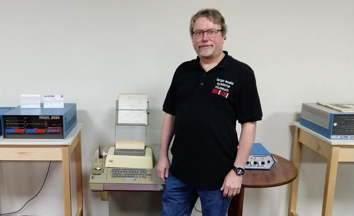
Corey Little, curator of the microcomputer collection, in front of Imsai, ASR-33 teletype, Kenbek-1 replica, and Altair.

Corey Little, curator of the microcomputer collection, in front of Imsai, ASR-33 teletype, Kenbek-1 replica, and Altair.

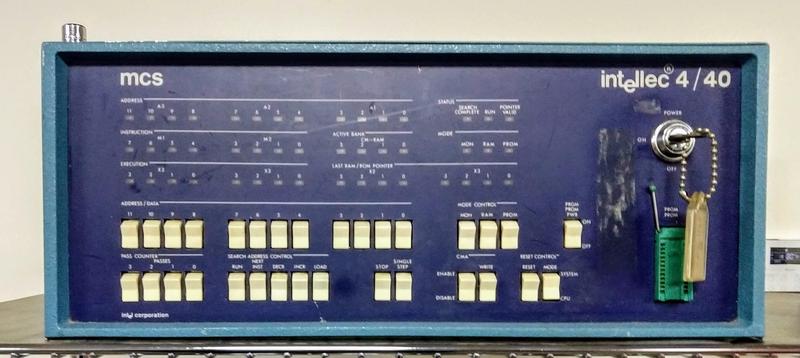
The first commercial microprocessor was Intel's 4-bit 4004, introduced in 1971. The Intel Intellec 4/40 development system (below), used the 4040 microprocessor (1974), an improved version of the 4004. This system was intended for engineers to develop software for embedded systems using the 4040 chip.

Intel Intellec 4/40 development system. An EPROM socket below the key allowed software to be burned into EPROM chips.

Intel Intellec 4/40 development system. An EPROM socket below the key allowed software to be burned into EPROM chips.

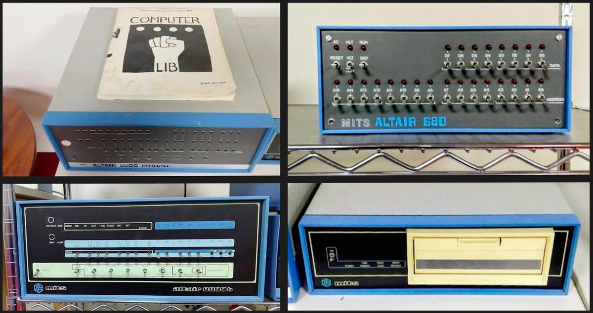
The microcomputer revolution took off when Intel released the 8-bit 8080 microprocessor in 1974, leading to the first commercially successful personal computer, the MITS Altair 8800 kit (1975). In addition to the Altair 8800, the museum has the updated Altair 8800b and the more obscure Altair 680, which uses the Motorola 6800 microprocessor.

Altair 8800 (with the famous manifesto Computer Lib on top), Altair 680, Altair 8800b, and disk drive for Altair.

Altair 8800 (with the famous manifesto Computer Lib on top), Altair 680, Altair 8800b, and disk drive for Altair.

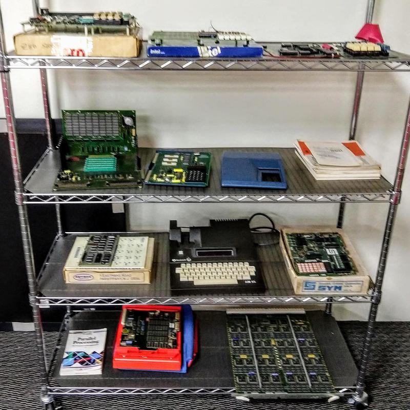
Single-board computers also helped popularize microprocessors. Companies produced development kits for engineers to experiment with new microprocessors and hobbyists often used them due to their low cost. The museum has several racks of these development boards; the rack below includes the Intel SDK-85 System Design Kit for the 8085 microprocessor, Artisan Electronics Model 85 microcalculator (a single-board scientific calculator that could be interfaced to a microcomputer), Rockwell's 6502-based AIM-65, Synertek's 6502-based SYM-1, and Transputer parallel processor boards.

A variety of development boards and single-board computers.

A variety of development boards and single-board computers.

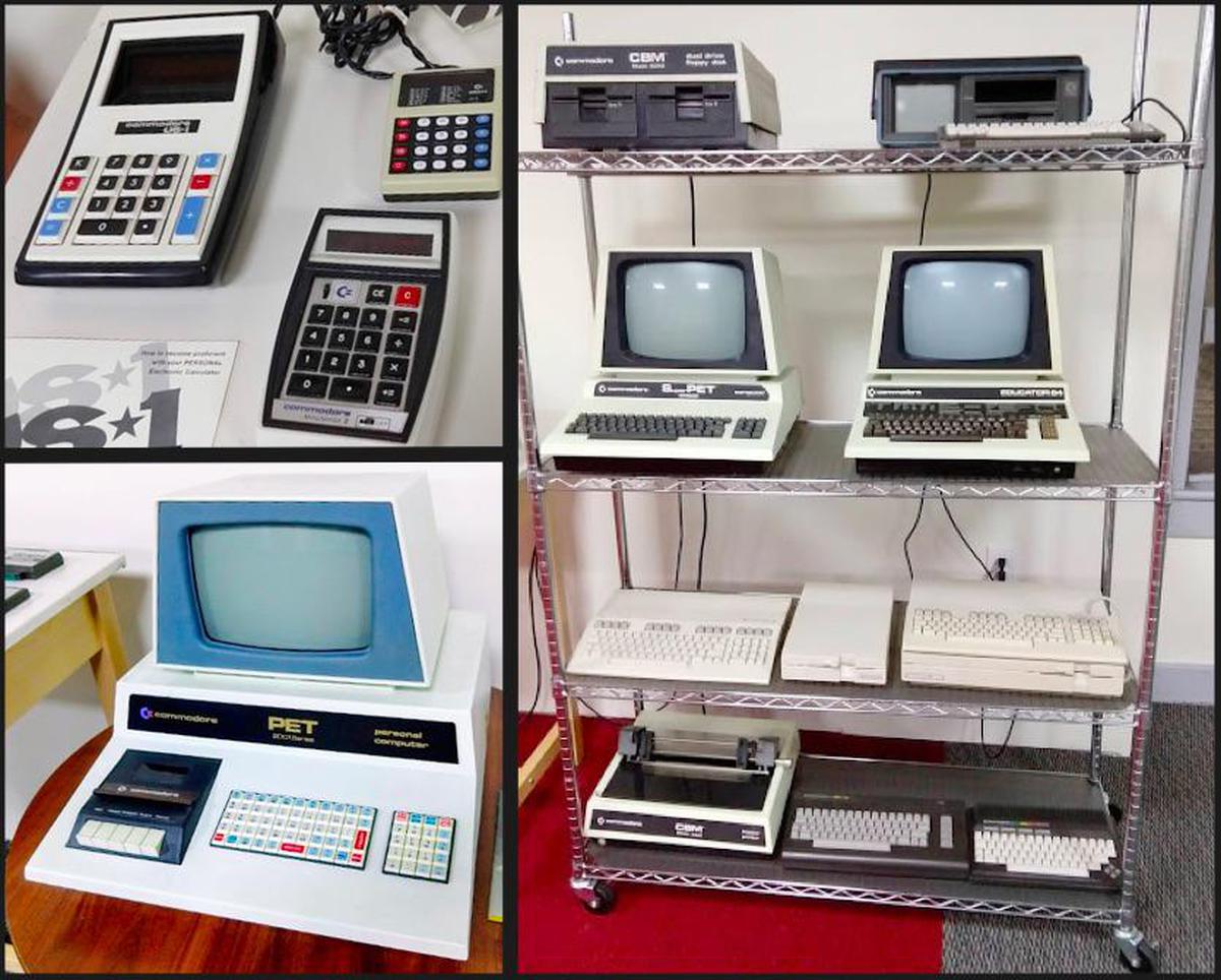
By the late 1970s, microcomputers became mass-market products, with the introduction of home computers that were more affordable and usable by the general public. The museum has many other popular home computers from manufacturers such as Atari, Sinclair, Radio Shack, Heathkit, and Texas Instruments. The photo below shows part of the Commodore collection.

The Commodore collection includes calculators, Commodore Super PET, Educator 64, PET 4032, and PET 2001

The Commodore collection includes calculators, Commodore Super PET, Educator 64, PET 4032, and PET 2001

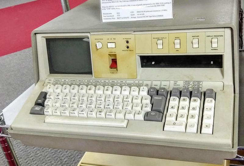
Early portable computers were suitcase-sized and often called luggables. The museum has a large collection including the IBM 5100 (1975; below), Osborne One (1981), Osborne Executive, Osborne Vixen, and Kaypro II, as well as more obscure machines such as the Telcon Zorba and General Electric Workmaster.

The IBM 5100 portable computer was introduced in 1975, six years before the IBM PC. Its keyboard has special characters for the APL language.

The IBM 5100 portable computer was introduced in 1975, six years before the IBM PC. Its keyboard has special characters for the APL language.

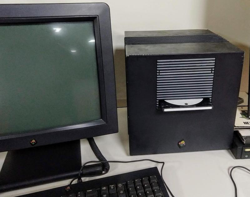
Apple is represented by a variety of Apple II, Apple III, Lisa, and Macintosh systems. The collection also includes a NeXTcube, the workstation developed by Steve Jobs in the 1980s after he was forced out of Apple. Steve Jobs returned to Apple when Apple purchased NeXT in 1997, leading to Apple's dramatic rise. The NeXTcube's operating system led to Apple's current macOS and iOS operating systems.

The NeXTcube workstation was packaged in a 1-foot magnesium cube.

The NeXTcube workstation was packaged in a 1-foot magnesium cube.

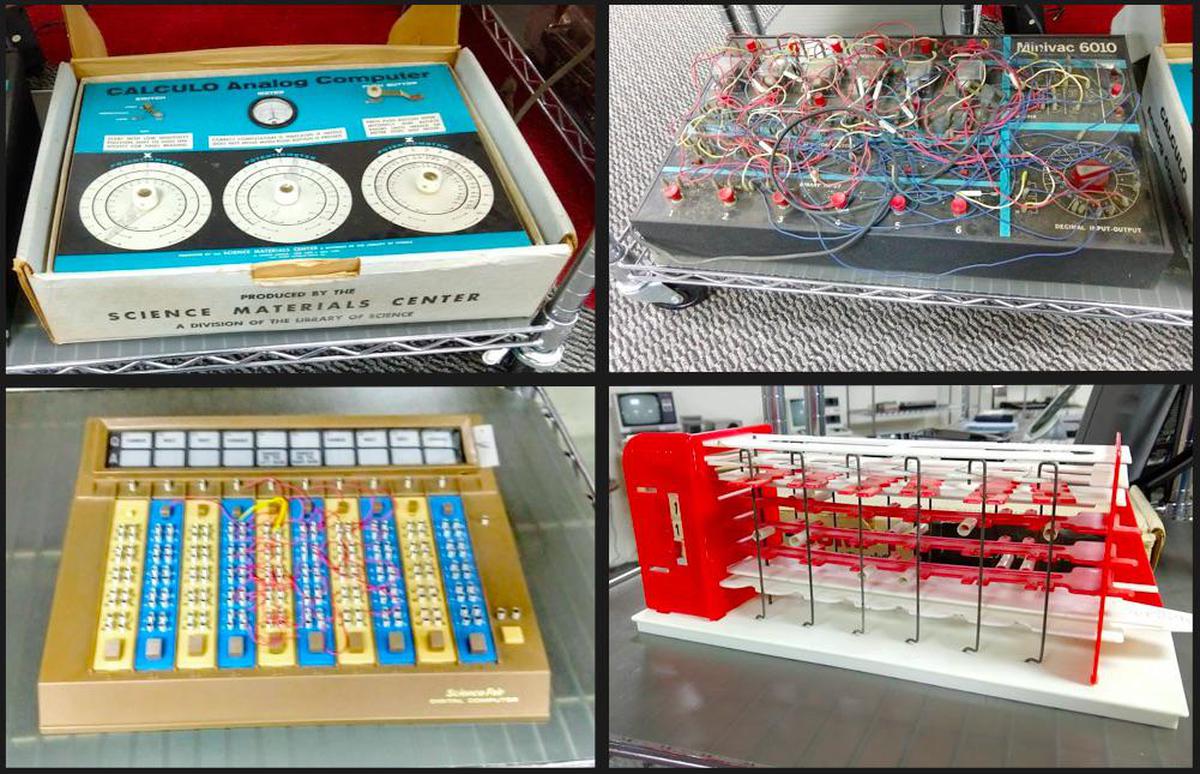
The museum has various toys and educational devices that were produced to explain computers, including the CALCULO Analog Computer (1959), Minivac 6010 (1962) created by the father of information theory Claude Shannon, Radio Shack Science Fair Digital Computer Kit (1977), and Digi-Comp 1 (1963).

The collection includes toy computers such as the CALCULO Analog Computer, MINIVAC 6010, Radio Shack ScienceFair Digital Computer, and Digi-Comp 1.

The collection includes toy computers such as the CALCULO Analog Computer, MINIVAC 6010, Radio Shack ScienceFair Digital Computer, and Digi-Comp 1.

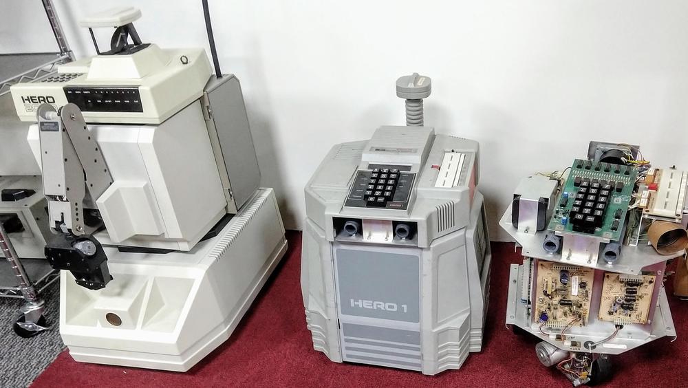
Heathkit introduced the HERO-1 kit robot in 1982, providing a way for hobbyists to experiment with robotics. Nowadays, Arduinos and cheap servos and stepper motors make it easy to build a simple robot, but in 1982, robotics was much more difficult. The HERO-1 kit cost $1500 (equivalent to about $4000 today).

Three Heathkit HERO robots. The HERO 2000 (1986, left) included multiple processors and speech synthesis, while the older HERO-1 robots have a single 6808 processor. The "eyes" are an ultrasonic distance sensor.

Three Heathkit HERO robots. The HERO 2000 (1986, left) included multiple processors and speech synthesis, while the older HERO-1 robots have a single 6808 processor. The "eyes" are an ultrasonic distance sensor.

Conclusion

The Large Scale Systems Museum contains a remarkable collection of large computer systems and microcomputers from the 1970s to 1990s The museum, hidden behind a storefront on a quiet small-town main street, illustrates an interesting period in computer history. During this time, mainframes, minicomputers, and supercomputers reached their peak and then went into steep decline. Meanwhile, the microprocessor passed through the hobbyist phase and the home computer phase before achieving its dominance. Amazingly most of the systems at the museum are up and running, giving the visitor a feel for the computers of that era.

The museum is open by appointment only; details are here and on their Facebook page. If you ever find yourself near New Kensington, PA (half an hour outside Pittsburgh), get in touch with them. I've only presented the highlights of the museum; more photos are here. I announce my latest blog posts on Twitter, so follow me @kenshirriff for future articles. I also have an RSS feed.

A computer built from NOR gates: inside the Apollo Guidance Computer

We recently restored an Apollo Guidance Computer1, the computer that provided guidance, navigation, and control onboard the Apollo flights to the Moon. This historic computer was one of the first to use integrated circuits and its CPU was built entirely from NOR gates.2 In this blog post, I describe the architecture and circuitry of the CPU.

Architecture of the Apollo Guidance Computer
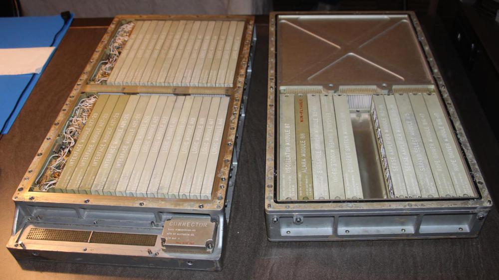
The Apollo Guidance Computer with the two trays separated. The tray on the left holds the logic circuitry built from NOR gates. The tray on the right holds memory and supporting circuitry.

The Apollo Guidance Computer with the two trays separated. The tray on the left holds the logic circuitry built from NOR gates. The tray on the right holds memory and supporting circuitry.

The Apollo Guidance Computer was developed in the 1960s for the Apollo missions to the Moon. In an era when most computers ranged from refrigerator-sized to room-sized, the Apollo Guidance Computer was unusual—small enough to fit onboard the Apollo spacecraft, weighing 70 pounds and under a cubic foot in size.

The AGC is a 15-bit computer. It may seem bizarre to have a word size that isn't a power of two, but in the 1960s before bytes became popular, computers used a wide variety of word sizes. In the case of the AGC, 15 bits provided sufficient accuracy to land on the moon (using double- and triple-precision values as needed), so 16 bits would have increased the size and weight of the computer unnecessarily.4

The Apollo Guidance Computer has a fairly basic architecture, even by 1960s standards. Although it was built in the era of complex, powerful mainframes, the Apollo Guidance Computer had limited performance; it is more similar to an early microprocessor in power and architecture.3 The AGC's strengths were its compact size and extensive real-time I/O capability. (I'll discuss I/O in another article.)5

The architecture diagram below shows the main components of the AGC. The parts I'll focus on are highlighted. The AGC has a small set of registers, along with a simple arithmetic unit that only does addition. It has just 36K words of ROM (fixed memory) and 2K words of RAM (erasable memory). The "write bus" was the main communication path between the components. Instruction decoding and the sequence generator produced the control pulses that directed the AGC.
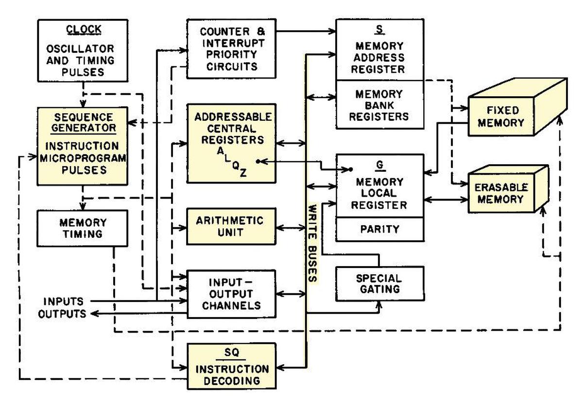
Block diagram of the Apollo Guidance Computer. From Space Navigation Guidance and Control, R-500, VI-14.

Block diagram of the Apollo Guidance Computer. From Space Navigation Guidance and Control, R-500, VI-14.

About half of the architecture diagram is taken up by memory, reflecting that in many ways the architecture of the Apollo Guidance Computer was designed around its memory. Like most computers of the 1960s, the AGC used core memory, storing each bit in a tiny ferrite ring (core) threaded onto a grid of wires. (Because a separate physical core was required for every bit, core memory capacity was drastically smaller than modern semiconductor memory.) A property of core memory was that reading a word from memory erased that word, so a value had to be written back to memory after each access. The AGC also had fixed (ROM), the famous core ropes used for program storage where bits were physically woven into the wiring pattern (below). (I've written about the AGC's core memory and core rope memory in detail.)
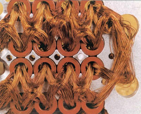
Detail of core rope memory wiring from an early (Block I) Apollo Guidance Computer. Photo from Raytheon.

Detail of core rope memory wiring from an early (Block I) Apollo Guidance Computer. Photo from Raytheon.

NOR gates

The Apollo Guidance Computer was one of the very first computers to use integrated circuits. These early ICs were very limited; the AGC's chips (below)2 contained just six transistors and eight resistors, implementing two 3-input NOR gates.
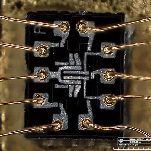
Die photo of the dual 3-input NOR gate used in the AGC. The ten bond wires around the outside of the die connect to the IC's external pins. Photo by Lisa Young, Smithsonian.

Die photo of the dual 3-input NOR gate used in the AGC. The ten bond wires around the outside of the die connect to the IC's external pins. Photo by Lisa Young, Smithsonian.

The symbol for a NOR gate is shown below. It is a very simple logic gate: if all inputs are low, the output is high. It might be surprising that NOR gates are sufficient to build a computer, but NOR is a universal gate: you can make any other logic gate out of NOR gates. For instance, wiring the inputs of a NOR gate together forms an inverter. Putting an inverter on the output of a NOR gate produces an OR gate. Putting inverters on the inputs of a NOR gate produces an AND gate.6 More complex circuits, such as flip flops, adders, and counters can be built from these gates.
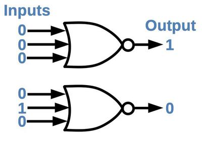
The NOR gate generates a 1 output if all inputs are 0. If any input is a 1 (or multiple inputs), the NOR gate generates a 0 output.

The NOR gate generates a 1 output if all inputs are 0. If any input is a 1 (or multiple inputs), the NOR gate generates a 0 output.

One building block that appears frequently in the AGC is the set-reset latch. This simple circuit is built from two NOR gates and stores one bit of data: the set input stores a 1 bit and the reset input stores a 0 bit. In more detail, a 1 pulse on the set input turns the top NOR gate off and the bottom one on, so the output is a 1. A 1 pulse on the reset input does the opposite so the output is a 0. If both inputs are 0, the latch remembers its previous state, providing storage. The next section will show how the latch circuit is used to build registers.
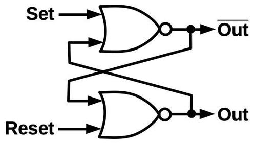
A set-reset latch built from two NOR gates. If one NOR gate is on, it forces the other one off. The overbar on the top output indicates that it is the complement of the lower output.

A set-reset latch built from two NOR gates. If one NOR gate is on, it forces the other one off. The overbar on the top output indicates that it is the complement of the lower output.

The registers

The Apollo Guidance Computer has a small set of registers to store values temporarily outside of core memory. The main register is the accumulator (A), which is used in many arithmetic operations. The AGC also has a program counter register (Z), arithmetic unit registers (X and Y), a buffer register (B), return address register (Q)7, and a few others. For memory accesses, the AGC has a memory address register (S) and a memory buffer register (G) for data. The AGC also has some registers that reside in core memory, such as I/O counters.

The following diagram outlines the register circuitry for the AGC, simplified to a single bit and two registers (Q and Z). Each register bit has a latch (flip-flop), using the circuit described earlier (blue and purple). Data is transmitted both to and from the registers on the write bus (red). To write to a register, the latch is first reset by a clear signal (CQG or CZG, green). A "write service" gate signal (WQG or WZG, orange) then allows the data on the write bus to set the corresponding register latch. To read a register, a "read service" gate signal (RQG or RZG, cyan) passes the latch's output through the write amplifier to the write bus, for use by other parts of the AGC. The complete register circuitry is more complex, with multiple 16-bit registers, but follows this basic structure.
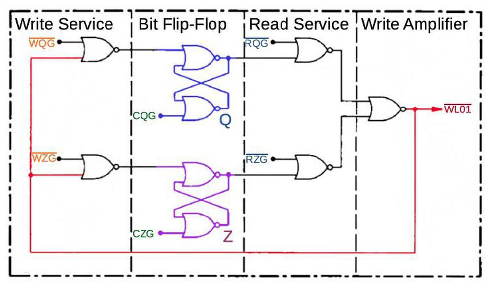
Simplified diagram of AGC register structure, showing one bit of the Q and Z registers. (Source)

Simplified diagram of AGC register structure, showing one bit of the Q and Z registers. (Source)

The register diagram illustrates three key points. First, the register circuitry is built from NOR gates. Second, data movement through the AGC centers on the write bus. Finally, the register actions (like other AGC actions) depend on specific control signals at the right time; the "control" section of this post will discuss how these signals are generated.

The arithmetic unit

Most computers have an arithmetic logic unit (ALU) that performs arithmetic and Boolean logic operations. Compared to most computers, the AGC's arithmetic unit is very limited: the only operation it performs is addition of 16-bit values, so it's called an arithmetic unit, not an arithmetic logic unit. (Despite its limited arithmetic unit, the AGC can perform a variety of arithmetic and logic operations including multiplication and division, as explained in the footnote.9)

The schematic below shows one bit of the AGC's arithmetic unit. The full adder (red) computes the sum of two bits and a carry. In particular, the adder sums the X bit, Y bit, and carry-in, generating the sum bit (sent to the write bus) and carry bit. The carry is passed to the next adder, allowing adders to be combined to add longer words.8)

Schematic of one bit in the AGC's arithmetic unit. (Based on AGC handbook p214.)

Schematic of one bit in the AGC's arithmetic unit. (Based on AGC handbook p214.)

The X register and Y register (purple and green) provide the two inputs to the adder. These are implemented with the NOR-gate latch circuits described earlier. The circuitry in blue writes a value to the X or Y register as specified by the control signals. This circuitry is fairly complex since it allows constants and shifted values to be stored in the registers, but I won't go into the details. Note the "A2X" control signal that gates the A register value into the X register; it will be important in the following discussion.

The photo below shows the physical implementation of the AGC's circuitry. This module implements four bits of the registers and arithmetic unit. The flat-pack ICs are the black rectangles; each module has two boards with 60 chips each, for a total of 240 NOR gates. The arithmetic unit and registers are built from four identical modules, each handling four bits; this is similar to a bit-slice processor.

The arithmetic unit and registers are implemented in four identical modules. Each module implements 4 bits. The modules are installed in slots A8 through A11 of the AGC.

The arithmetic unit and registers are implemented in four identical modules. Each module implements 4 bits. The modules are installed in slots A8 through A11 of the AGC.

Executing an instruction

This section illustrates the sequence of operations that the AGC performs to execute an instruction. In particular, I'll show how an addition instruction, ADS (add to storage), takes place. This instruction reads a value from memory, adds it to the accumulator (A register), and stores the sum in both the accumulator and memory. This is a single machine instruction, but the AGC performs many steps and many values move back and forth to accomplish it.

Instruction timing is driven by the core memory subsystem. In particular, reading a value from core memory erases the stored value, so a value must be written back after each read. Also, when accessing core memory there is a delay between when the address is set up and when the data is available. The result is that each memory cycle takes 12 time steps to perform first a read and then a write. Each time interval (T1 to T12) takes just under one microsecond, and the full memory cycle takes 11.7µs, called a Memory Cycle Time (MCT).

The erasable core memory module from the Apollo Guidance Computer. This module holds 2 kilowords of memory, with a tiny ferrite core storing each bit. To read memory, high-current pulses flip the magnetization of the cores, erasing the word.

The erasable core memory module from the Apollo Guidance Computer. This module holds 2 kilowords of memory, with a tiny ferrite core storing each bit. To read memory, high-current pulses flip the magnetization of the cores, erasing the word.

The MCT is the basic time unit for instruction execution. A typical instruction requires two memory cycles: one memory access to fetch the instruction from memory, and one memory access to perform the operation.13 Thus, a typical instruction requires two MCTs (23.4µs), yielding about 43,000 instructions per second. (This is extremely slow compared to modern processors performing billions of instructions per second.)

Internally, the Apollo Guidance Computer processes instructions by breaking an instruction into subinstructions, where each subinstruction takes one memory cycle For example, the ADS instruction consists of two subinstructions: the ADS0 subinstruction (which does the addition) and the STD2 subinstruction (which fetches the next instruction, and is common to most instructions). The diagram below shows the data movement inside the AGC to execute the ADS0 subinstruction. The 12 times steps are indicated left to right.
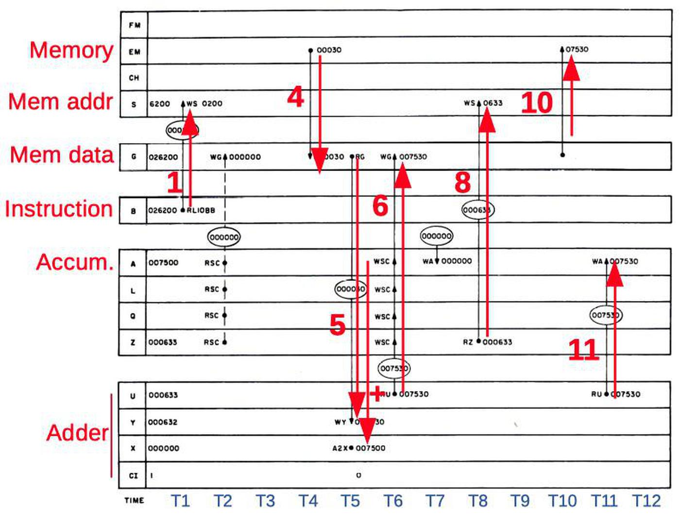
Operations during the ADS0 (add to storage) subinstruction. Arrows show important data movement. Based on the manual.

Operations during the ADS0 (add to storage) subinstruction. Arrows show important data movement. Based on the manual.

The important steps are:
T1: The operand address is copied from the instruction register (B) to the memory address register (S) to start a memory read.
T4: The operand is read from core memory to the memory data register (G).
T5: The operand is copied from (G) to the adder (Y). The accumulator value (A) is copied to the adder (X).
T6: The adder computes the sum (U), which is copied to the memory data register (G).
T8: The program counter (Z) is copied to the memory address register (S) to prepare for fetching the next instruction from core memory.
T10: The sum in the memory data register (G) is written back to core memory.
T11: The sum (U) is copied to the accumulator (A).

Even though this is a simple add instruction, many values are moved around during the 12 time intervals. Each of these actions has a control signal associated with it; for instance, the signal A2X at time T5 causes the accumulator (A) value to be copied to the X register. Copying the G register to the Y register takes two control pulses: RG (read G) and WY (write Y). The next section will explain how the AGC's control unit generates the appropriate control signals for each instruction, focusing on these A2X, RG, and WY control pulses needed by ADS0 at time T5.

The control unit

As in most computers, the AGC's control unit decodes each instruction and generates the control signals that tell the rest of the processor (the datapath) what to do. The AGC is designed with microcoded approach, but the control signals are generated from a hardwired control unit built from NOR gates. Specifically, there are no microinstructions and the AGC does not have a control store holding microcode (which would have taken too much physical space).12You can think of the AGC as implementing the microcode ROM with highly-optimized logic gates.

The heart of the AGC's control unit is called the crosspoint generator. Conceptually, the crosspoint generator takes the subinstruction and the time step, and generates the control signals for that combination of subinstruction and time step. (You can think of the crosspoint generator as a grid with subinstructions in one direction and time steps in the other, with control signals assigned to each point where the lines cross.) For instance, going back to the ADS0 subinstruction, at time T5 the crosspoint generator would generate the A2X, RG, and WY control pulses, causing the desired data movement.

The crosspoint generator required a lot of circuitry and was split across three modules; this is module A6. Note the added wires to modify the circuitry. This is an earlier module used for ground testing; modules in flight did not have these wires.

The crosspoint generator required a lot of circuitry and was split across three modules; this is module A6. Note the added wires to modify the circuitry. This is an earlier module used for ground testing; modules in flight did not have these wires.

For efficiency, the implementation of the control unit is highly optimized. Instructions with similar behavior are combined and processed together by the crosspoint generator to reduce circuitry. For instance, the AGC has a "Double-precision Add to Storage" instruction (DAS). Since this is roughly similar to performing two single-word adds, the DAS1 subinstruction and ADS0 subinstruction share logic in the crosspoint generator. The schematic below shows the crosspoint generator circuitry for time T5, highlighting the logic for subinstruction ADS0 (using the DAS1 signal). For instance, the 5K signal is generated from the combination of DAS1 and T5.
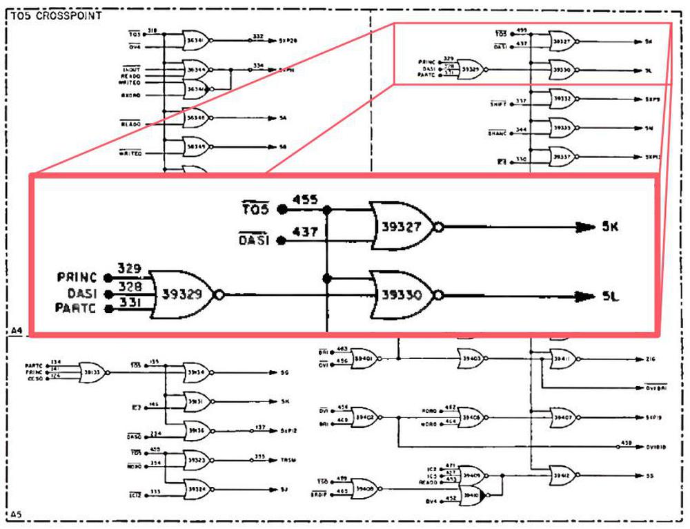
Crosspoint circuit for signals generated at time T5. With negative inputs, these NOR gates act as AND gates, detecting a particular subinstruction AND T05. From Apollo Lunar Excursion Manual.

Crosspoint circuit for signals generated at time T5. With negative inputs, these NOR gates act as AND gates, detecting a particular subinstruction AND T05. From Apollo Lunar Excursion Manual.

But what are the 5K and 5L signals? These are another optimization. Many control pulses often occur together, so instead of generating all the control pulses directly, the crosspoint generates intermediate crosspoint signals. For instance, 5K generates both the A2X and RG control pulses, while 5L generates the WY control pulse. The diagram below shows how the A2X signal is generated: any of 8 different signals (including 5K) generate A2X.15 Similar circuits generate the other control pulses. These optimizations reduced the size of the crosspoint generator, but it was still large, split across three modules in the AGC.
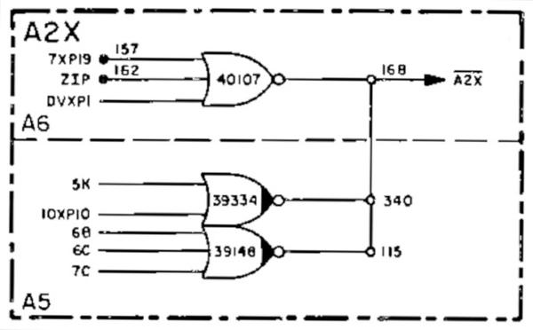
The A2X control signal is generated from multiple "crosspoint pulses" from the crosspoint generator. The different possibilities are ORed together. From manual, page 4-351.

The A2X control signal is generated from multiple "crosspoint pulses" from the crosspoint generator. The different possibilities are ORed together. From manual, page 4-351.

To summarize, the control unit is responsible for telling the rest of the CPU what to do in order to execute an instruction. Instructions are first decoded into subinstructions. The crosspoint generator creates the proper control pulses for each time interval and subinstruction, telling the AGC's registers, arithmetic unit, and memory what to do.14

Conclusion

This has been a whirlwind tour of the Apollo Guidance Computer's CPU. To keep it manageable, I've focused on the ADS addition instruction and a few of the control pulses (A2X, RG, and WY) that make it operate. Hopefully, this gives you an idea of how a computer can be built from components as primitive as NOR gates.

The most visible part of the architecture is the datapath: arithmetic unit, registers, and the data bus. The AGC's registers are built from simple NOR-gate latches. Even though the AGC's arithmetic unit can only do addition, the computer still manages to perform a full set of operations including multiplication and division and Boolean operations.9

However, the datapath is just part of the computer. The other critical component is the control unit, which tells the data path components what to do. The AGC uses an approach centered around a crosspoint generator, which uses highly-optimized hardwired logic to generate the right control pulses for a particular subinstruction and time interval.

Using these pieces, the Apollo Guidance Computer provided guidance, navigation, and control onboard the Apollo missions, making the Moon landings possible. The AGC also provided a huge boost to the early integrated circuit industry, using 60% of the United States' IC production in 1963. Thus, modern computers owe a lot to the AGC and its simple NOR gate components.
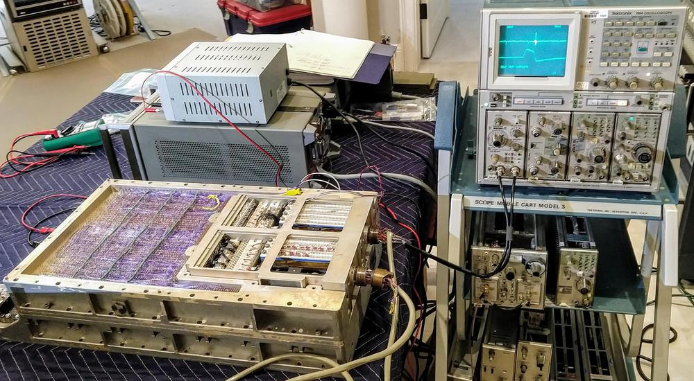
The Apollo Guidance Computer running in Marc's lab, hooked up to a vintage Tektronix scope.

The Apollo Guidance Computer running in Marc's lab, hooked up to a vintage Tektronix scope.

CuriousMarc has a series of AGC videos which you should watch for more information on the restoration project. I announce my latest blog posts on Twitter, so follow me @kenshirriff for future articles. I also have an RSS feed. Thanks to Mike Stewart for supplying images and extensive information.

Notes and references

  1. The AGC restoration team consists of Mike Stewart (creator of FPGA AGC), Carl Claunch, Marc Verdiell (CuriousMarc on YouTube) and myself. The AGC that we're restoring belongs to a private owner who picked it up at a scrapyard in the 1970s after NASA scrapped it. 

  2. In addition to the NOR-gate logic chips, the AGC used a second type of integrated circuit for its memory circuitry, a sense amplifier. (The earlier Block I Apollo Guidance Computer used NOR gate ICs that contained a single NOR gate.) 

  3. How does the AGC stack up to early microprocessors? Architecturally, I'd say it was more advanced than early 8-bit processors like the 6502 (1975) or Z-80 (1976), since the AGC had 15 bits instead of 8, as well as more advanced instructions such as multiplication and division. But I consider the AGC less advanced than the 16-bit Intel 8086 (1978) which has a larger register set, advanced indexing, and instruction queue. Note, though, that the AGC was in a class of its own as far as I/O, with 227 interface circuits connected to the rest of the spacecraft.

    Looking at transistor counts, the Apollo Guidance Computer had about 17,000 transistors in total in its ICs, which puts it between the Z80 microprocessor (8,500 transistors) and the Intel 8086 (29,000 transistors).

    As far as performance, the AGC did a 15-bit add in 23.4μs and a multiply in 46.8μs. The 6502 took about 3.9μs for an 8-bit add (much faster, but a smaller word). Implementing an 8-bit multiply loop on the 6502 might take over 100μs, considerably worse than the AGC. The AGC's processor cycle speed of 1.024 MHz was almost exactly the same as the Apple II's 1.023 MHz clock, but the AGC took 24 cycles for a typical instruction, compared to 4 on the 6502. The big limitation on AGC performance was the 11.7μs memory cycle time, compared to 300 ns for the Apple II's 4116 DRAM chips.  

  4. An AGC instruction fit into a 15-bit word and consisted of a 3-bit opcode and a 12-bit memory address. Unfortunately, both the opcode and memory address were too small, resulting in multiple workarounds that make the architecture kind of clunky.

    The AGC's 15-bit instructions included a 12-bit memory address which could only address 4K words. This was inconvenient since the AGC had 2K words of core RAM and 36K words of core rope ROM. To access this memory with a 12-bit address, the AGC used a complex bank-switching scheme with multiple bank registers. In other words, you could only access RAM in 256-word chunks and ROM in somewhat larger chunks.

    The AGC's instructions had a 3-bit opcode field, which was too small to directly specify the AGC's 34 instructions. The AGC used several tricks to specify more opcodes. First, an EXTEND instruction changed the meaning of the following instruction, allowing twice as many opcodes but wasting a word. Also, some AGC opcodes didn't make sense if performed on a ROM address (such as incrementing), so four different instructions ("quartercode instructions") could share an opcode field. Instructions that act on peripherals only use 9 address bits, freeing up 3 additional bits for opcode use. This allows, for instance, Boolean operations (AND, OR, XOR) to fit into the opcode space, but they can only access peripheral addresses, not main memory addresses.

    The AGC also used some techniques to keep the opcode count small. For example, it had some "magic" memory locations such as the "shift right register". Writing to this address performed a shift; this avoided a separate opcode for "shift right".

    The AGC also had some instructions that wedged multiple functions into a single instruction. For instance, the "Transfer to Storage" instruction not only transferred a value to storage, but also checked the overflow flag and updated the accumulator and skipped an instruction if there had been an arithmetic overflow. Another complex instruction was "Count, Compare, and Skip", which loaded a value from memory, decremented it, and did a four-way branch depending on its value. See AGC instruction set for details. 

  5. For more on the AGC's architecture, see the Virtual AGC and the Ultimate Apollo Guidance Computer Talk

  6. The NAND gate also has the same property of being a universal gate. (In modern circuits, NAND gates are usually more popular than NOR gates for technical reasons.) The popular NAND to Tetris course describes how to build up a computer from NAND gates, ending with an implementation of Tetris. This approach starts by building a set of logic gates (NOT, AND, OR, XOR, multiplexer, demultiplexer) from NAND gates. Then larger building blocks (flip flop, adder, incrementer, ALU, register) are built from these gates, and finally a computer is built from these building blocks. 

  7. Modern computers usually have a stack that is used for subroutine calling and returning. However, the AGC (like many other computers of its era) didn't have a stack, but stored the return address in a link register (the AGC's Q register). To use recursion, a programmer would need to implement their own stack. 

  8. A carry-skip circuit improves the performance of the adder. The problem with binary addition is that propagating a carry through all the bits is slow. For example, if you add 111111111111111 + 1, the carry from the low-order bit gets added to the next bit. This generates a carry which propagates to the next bit, and so forth. This "ripple carry" causes the addition to be essentially one bit at a time. To avoid this problem, the AGC uses a carry-skip circuit that looks at groups of four bits. If there is a carry in, and each position has at least one bit set, there is certain to be a carry, so a carry-out is generated immediately. Thus, propagating a carry is approximately three times as fast. (With groups of four bits, you'd expect four times as fast, but the carry-skip circuit has its own overhead.) 

  9. You might wonder how the AGC performs a variety of arithmetic and logic operations if the arithmetic unit only supports addition. Subtraction is performed by complementing one value (i.e. flipping the bits) and then adding. Most computers have a complement circuit built into the ALU, but the AGC is different: when the B register is read, it can provide either the value or the complement of the stored value.10 So to subtract a value, the value is stored in the B register and then the complement is read out and added.

    What about Boolean functions? While most computers implement Boolean functions with logic circuitry in the ALU, the Apollo Guidance Computer manages to implement them without extra hardware. The OR operation is implemented through a trick of the register circuitry. By gating two registers onto the write bus at the same time, a 1 from either register will set the bus high, yielding the OR of the two values. AND is performed using the formula A ∧ H = ~(~A ∨ ~H); complementing both arguments, doing an OR, and then complementing the result yields the AND operation. XOR is computed using the formula A ⊕ H = ~(A ∨ ~H) ∨ ~(H ∨ ~A), which uses only complements and ORs. It may seem inefficient to perform so many complement and OR operations, but since the instruction has to take 12 time intervals in any case (due to memory timing), the multiple steps don't slow down the instruction.

    Multiplication is performed by repeated additions, subtractions, and shifts using a Radix-4 Booth algorithm that operates two bits at a time. Division is performed by repeated subtractions and shifts.11 Since multiply and divide require multiple steps internally, they are slower than other arithmetic instructions. 

  10. Since a latch has outputs for both a bit and the complement of the bit, it is straightforward to get the complemented value out of a latch. Look near the bottom of the schematic to see the B register's circuitry that provides the complemented value. 

  11. The AGC's division algorithm is a bit unusual. Instead of subtracting the divisor at each step, a negative dividend / remainder is used through the division and the divisor is added. (This is essentially the same as subtracting the divisor, except everything is complemented.) See Block II Machine Instructions section 32-158 for details. 

  12. The AGC doesn't use microcode but confusingly some sources say it was microprogrammed. The book "Journey to the Moon" by Eldon Hall (creator of the AGC) says:

    The instruction selection logic and control matrix was a microprogrammed instruction sequence generator, equivalent to a read-only memory implemented in logic. Outputs of the microprogrammed memory were a sequence of control pulses that were logic products of timing pulses, tests of priority activity, instruction code, and memory address.

    This doesn't make sense, since the whole point of microprogramming is to use read-only memory instead of hardwired control logic. (See A brief history of microprogramming, Computer architecture: A quantitative approach section 5.4, or Microprogramming: principles and practices.) Perhaps Hall means that the AGC's control was "inspired" by microprogramming, using a clearly-stated set of sequenced control signals with control hardware separated from the data path (like most modern computers, hardwired or microcoded). (In contrast, in many 1950s computers (like the IBM 1401) each instruction's circuitry generated its own ad hoc control signals.)

    By the way, implementing the AGC in microcode would have required about 8 kilobytes of microcode (79 control pulses for about 70 subinstructions with 12 time periods. This would have been impractical for the AGC, especially when you consider that microcode storage needs to be faster than regular storage.  

  13. While instructions typically used two subinstructions, there were exceptions. Some instructions, such as multiply and divide, required multiple subinstructions because they took many steps. On the other hand, the jump instruction (TC) used a single subinstruction since fetching the next instruction was the only task to do. 

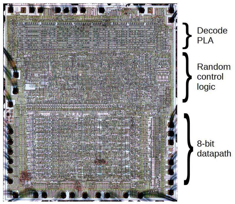
  14. Other processors use different approaches to generate control signals. The 6502 and many other early microprocessors decoded instructions with a Programmable Logic Array (PLA), a ROM-like way of implementing AND-OR logic. The Z-80 used a PLA, followed by logic very similar to the crosspoint generator to generate the right signals for each time step. Many computers use microcode, storing the sequence of control steps explicitly in ROM. Since minimizing the number of chips in the AGC was critical, optimizing the circuitry was more important than using a clean, structured approach.

    Die photo of the 6502 microprocessor. The 6502 used a PLA and random logic for the control logic, which occupies over half the chip. Note the regular, grid-like structure of the PLA. Die photo courtesy of Visual 6502.

    Die photo of the 6502 microprocessor. The 6502 used a PLA and random logic for the control logic, which occupies over half the chip. Note the regular, grid-like structure of the PLA. Die photo courtesy of Visual 6502.


  15. Each subinstruction's actions at each time interval are described in the manual. The control pulses are described in detail in the manual. (The full set of control pulses for ADS0 are listed here.)