Reverse-engineering the 8085's decimal adjust circuitry

In this post I reverse-engineer and describe the simple decimal adjust circuit in the 8085 microprocessor. Binary-coded decimal arithmetic was an important performance feature on early microprocessors. The idea behind BCD is to store two 4-bit decimal numbers in a byte. For instance, the number 42 is represented in BCD as 0100 0010 (0x42) instead of binary 00101010 (0x2a). This continues my reverse engineering series on the 8085's ALU, flag logic, undocumented flags, register file, and instruction set.

The motivation behind BCD is to make working with decimal numbers easier. Programs usually need to input and output numbers in decimal, so if the number is stored in binary it must be converted to decimal for output. Since early microprocessors didn't have division instructions, converting a number from binary to decimal is moderately complex and slow. On the other hand, if a number is stored in BCD, outputting decimal digits is trivial. (Nowadays, the DAA operation is hardly ever used).

Photograph of the 8085 chip showing the location of the ALU, flags, and registers.

One problem with BCD is the 8085's ALU operates on binary numbers, not BCD. To support BCD operations, the 8085 provides a DAA (decimal adjust accumulator) operation that adjusts the result of an addition to correct any overflowing BCD values. For instance, adding 5 + 6 = binary 0000 1011 (hex 0x0b). The value needs to be corrected by adding 6 to yield hex 0x11. Adding 9 + 9 = binary 0001 0010 (hex 0x12) which is a valid BCD number, but the wrong one. Again, adding 6 fixes the value. In general, if the result is ≥ 10 or has a carry, it needs to be decimal adjusted by adding 6. Likewise, the upper 4 BCD bits get corrected by adding 0x60 as necessary. The DAA operation performs this adjustment by adding the appropriate value. (Note that the correction value 6 is the difference between a binary carry at 16 and a decimal carry at 10.)

The DAA operation in the 8085 is implemented by several components: a signal if the lower bits of the accumulator are ≥ 10, a signal if the upper bits are ≥ 10 (including any half carry from the lower bits), and circuits to load the ACT register with the proper correction constant 0x00, 0x06, 0x60, or 0x66. The DAA operation then simply uses the ALU to add the proper correction constant.

The block diagram below shows the relevant parts of the 8085: the ALU, the ACT (accumulator temp) register, the connection to the data bus (dbus), and the various control lines.

The accumulator and ACT (Accumulator Temporary) registers and their control lines in the 8085 microprocessor.

The circuit below implements this logic. If the low-order 4 bits of the ALU are 10 or more, alu_lo_ge_10 is set. The logic to compute this is fairly simple: the 8's place must be set, and either the 4's or 2's. If DAA is active, the low-order bits must be adjusted by 6 if either the low-order bits are ≥ 10 or there was a half-carry (A flag).

Similarly, alu_hi_ge_10 is set if the high-order 4 bits are 10 or more. However, a base-10 overflow from the low order bits will add 1 to the high-order value so a value of 9 will also set alu_hi_ge_10 if there's an overflow from the low-order bits. A decimal adjust is performed by loading 6 into the high-order bits of the ACT register and adding it. A carry out also triggers this decimal adjust.

Schematic of the decimal adjust circuitry in the 8085 microprocessor.

Schematic of the decimal adjust circuitry in the 8085 microprocessor.

The circuits to load the correction value into ACT are controlled by the load_act_x6 signal for the low digit and load_act_6x for the high digit. These circuits are shown in my earlier article Reverse-engineering the 8085's ALU and its hidden registers.

Comparison to the 6502

By reverse-engineering the 8085, we see how the simple decimal adjust circuit in the 8085 works. In comparison, the 6502 handles BCD in a much more efficient but complex way. The 6502 has a decimal mode flag that causes addition and subtraction to automatically do decimal correction, rather than using a separate instruction. This patented technique avoids the performance penalty of using a separate DAA instruction. To correct the result of a subtraction, the 6502 needs to subtract 6 (or equivalently add 10). The 6502 uses a fast adder circuit that does the necessary correction factor addition or subtraction without using the ALU. Finally, the 6502 determines if correction is needed before the original addition/subtraction completes, rather than examining the result of the addition/subtraction, providing an additional speedup.

This information is based on the 8085 reverse-engineering done by the visual 6502 team. This team dissolves chips in acid to remove the packaging and then takes many close-up photographs of the die inside. Pavel Zima converted these photographs into mask layer images, generated a transistor net from the layers, and wrote a transistor-level 8085 simulator.

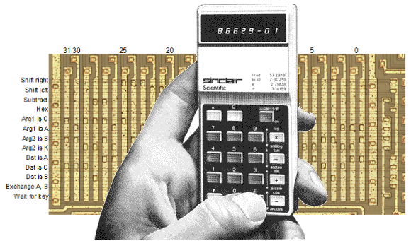
Reverse-engineering and simulating Sinclair's amazing 1974 calculator with half the ROM of the HP-35

I've reverse-engineered the Sinclair Scientific calculator. The remarkable thing about this calculator is they took a simple 4-function calculator chip and reprogrammed its 320-instruction ROM to be a full scientific calculator. By looking at the chip, I've extracted the original code, reverse-engineered how it works, and written a JavaScript simulator that runs the original code and shows what the calculator is doing internally.

The simulator is at righto.com/sinclair. My earlier TI calculator simulator is at righto.com/ti. (The image above is courtesy of Hackaday.)

I wouldn't have given a nickel for their stock: Visiting Apple in 1976

A guest posting from William Fine:

I saw the "Jobs" movie yesterday and it revived some ancient memories of my dealings with Jobs and Holt in the "old days"! When I returned home, I researched Rod Holt on the Internet and ran across your Power Supply Blog, which I found most interesting. Perhaps you can add my ensuing comments to your blog as you see fit.

In 1973 I started a company in my garage in Cupertino to design and manufacture custom Magnetic Products. It was called Mini-Magnetics Co. Inc. After a few months I was forced out of the garage into a small office complex on Sunnyvale-Saratoga Road, and had about 5/10 employees.

I believe it was around 1975/76 or so, I had a visit from a insulation and wire salesman named Mike Felix. He informed me that I may soon be getting a call from a new /start-up company called Apple Computer located just a few blocks away in Cupertino. He gave them my name when he was asked to recommend a Magnetics manufacturing house.

I promptly forgot about it, as I was already quite busy and I never had to solicit business or even advertise. A week or two went by, and I received a call from a female at Apple who set up a appointment for the next day with a guy named Steve Jobs. She gave me the address and it turned out to be located in a office complex located just behind the "Good Earth" restaurant.

The next day I went over to the location and knocked on the door, and it was opened by Jobs, with Wozniack in the background and a young hippie looking girl at a desk in the corner talking on the phone while eating. That was Apple Computer. They had just moved out of their garage into this new location. It appeared to be a large room with "stuff" scattered hap-hazardly all over, on benches and on the floor. From Jobs' appearance, I was a bit afraid to even shake hands with him, especially after getting a whiff of his body odor!

He immediately took me over to a bench that had a few cardboard boxes on it and showed me some transformer cores, bobbins and spools of wire, and unfolded a hand written diagram of the various magnetic components that he wanted me to wind and assemble for Apple.I took a quick look, and while it was all quite sketchy, looked do-able. He said that he needed them within 10 days and I said ok, since he was furnishing the materials.

I told him that I would call him with a quote after I got back to my office and he said ok and as we were parting he mentioned that if I had any technical questions to get a hold of a guy named Rod Holt and wrote down a phone number where he could be reached.

As I recall, there were about 5-6 magnetic components from simple toroids to a complex switching main power transformer. I believe that the price came to about $10.00 per set,and they wanted 35 sets, so the entire matter would be about $350.00. I called it into Apple the next day and they gave me a Purchase Order number over the phone. When I asked if they would be mailing me a hard copy confirming the order, they had no idea of what I was talking about!

I figured, what the hell, worst case, I would be out $350 bucks if they didn't pay the bill. No big deal.

After I got into examining the sketches I discovered something quite interesting about the power transformer. In all previous designs that I had seen, there was a primary, a base feedback winding and several output windings. What Holt had contrived was a interesting method of assuring excellent coupling of the base winding by using a single strand of wire from a multi-filar bundle that was custom ordered from the wire factory. For example, I think that there was a bundle of 30 strands twisted together, which were all coated in red insulation and one strand of green insulation also twisted together in the bundle, which gave a precise turns ratio together with excellent coupling between the windings.

I am uncertain if that contributed much to improving the efficiency of the switcher, but it seemed clever at the time I discovered it. That transformer, is the one that is shown with the copper foil external shield pictured in your blog. I did speak with Holt once or twice but never met him in person.

The 35 sets of parts were delivered on time and much to my surprise, we were paid within 10 days. I attributed that to the arrival of Mike Markkula onto the scene who had provided some money and organization to Apple.

At the time, after seeing the Apple operation, I wouldn't have given a nickle for a share of their stock if it had been offered! Ha!

I had been involved with power supplies for many years prior to this Apple issue, and can say that switchers were known for a long time, but only became practical with the advent of low loss ferrite core materials and faster transistors as your blog implies.

So, thats the Apple Power Supply story ! Be happy to answer any questions that you may come up with. Regards, wpf

Simulating a TI calculator with crazy 11-bit opcodes

I've built a register-level simulator of a 1974 TI calculator chip that shows what actually happens inside a calculator when you perform operations and shows the calculator source code as it executes. The architecture of the calculator chip is pretty interesting, with 11-bit opcodes, a 9-bit address bus, and 44-bit BCD registers. The chip doesn't support multiplication or division, so these are performed with repeated addition or subtraction.

The simulator is at righto.com/ti.

Reverse-engineering the 8085's ALU and its hidden registers

This article describes how the ALU of the 8085 microprocessor works and how it interacts with the rest of the chip, based on reverse-engineering of the silicon. (This is part 2 of my ALU reverse-engineering; part 1 described the circuit for a single ALU bit.) Along with the accumulator, the ALU uses two undocumented registers - ACT and TMP - and this article describes how they work in detail, as well as how the ALU is controlled.

The arithmetic-logic unit is a key part of the microprocessor, performing operations and comparisons on data. In the 8085, the ALU is also a key part of the data path for moving data. The ALU and associated registers take up a fairly large part of the chip, the upper left of the photomicrograph image below. The control circuitry for the ALU is in the top center of the image. The data bus (dbus) is indicated in blue.
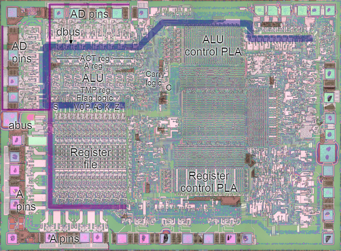
Photograph of the 8085 chip showing the location of the ALU, flags, and registers.

Photograph of the 8085 chip showing the location of the ALU, flags, and registers.

The real architecture of the 8085 ALU

The following architecture diagram shows how the ALU interacts with the rest of the 8085 at the block-diagram level. The data bus (dbus) conneccts the ALU and associated registers with the rest of the 8085 microprocessor. There are also numerous control lines, which are not shown.

The ALU uses two temporary registers that are not directly visible to the programmer. The Accumulator Temporary register (ACT) holds the accumulator value while an ALU operation is performed. This allows the accumulator to be updated with the new value without causing a race condition. The second temporary register (TMP) holds the other argument for the ALU operation. The TMP register typically holds a value from memory or another register.
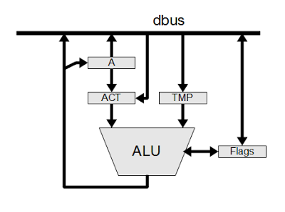
Architecture of the 8085 ALU as determined from reverse-engineering.

Architecture of the 8085 ALU as determined from reverse-engineering.

The 8085 datasheet has an architecture diagram that is simplified and not quite correct. In particular, the ACT register is omitted and a data path from the data bus to the accumulator is shown, even though that path doesn't exist.

The accumulator and ACT registers

To the programmer, the accumulator is the key register for arithmetic operations. Reverse-engineering, however, shows the accumulator is not connected directly to the ALU, but works closely with the ACT (accumulator temporary) register.

The ACT register has several important functions. First, it holds the input to the ALU. This allows the results from the ALU to be written back to the accumulator without disturbing the input, which would cause instability. Second, the ACT can hold constant values (e.g. for incrementing or decrementing, or decimal adjustment) without affecting the accumulator. Finally, the ACT allows ALU operations that don't use the accumulator.
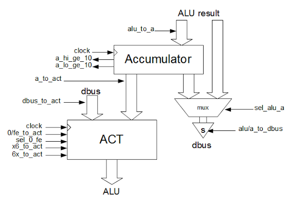
The accumulator and ACT (Accumulator Temporary) registers and their control lines in the 8085 microprocessor.

The accumulator and ACT (Accumulator Temporary) registers and their control lines in the 8085 microprocessor.

The diagram above shows how the accumulator and ACT registers are connected, and the control lines that affect them. One surprise is that the only way to put a value into the accumulator is through the ALU. This is controlled by the alu_to_a control line. You might expect that if you load a value into the accumulator, it would go directly from the data bus to the accumulator. Instead, the value is OR'd with 0 in the ALU and the result is stored in the accumulator.

The accumulator has two status outputs: a_hi_ge_10, if the four high-order bits are ≥ 10, and a_lo_ge_10, if the four low-order bits are ≥ 10. These outputs are used for decimal arithmetic, and will be explained in another article.

The accumulator value or the ALU result can be written to the databus through the sel_alu_a control (which selects between the ALU result and the accumulator), and the alu/a_to_dbus control line, which enables the superbuffer to write the value to the data bus. (Because the data bus is large and connects many parts of the chip, it requires high-current signals to overcome its capacitance. A "superbuffer" provides this high-current output.)

The ACT register can hold a variety of different values. In a typical arithmetic operation, the accumulator value is loaded into the ACT via the a_to_act control. The ACT can also load a value from the data bus via dbus_to_act. This is used for the ARHL/DAD/DSUB/LDHI/LDSI/RDEL instructions (all of which are undocumented except DAD). These instructions perform arithmetic operations without involving the accumulator, so they require a path into the ALU that bypasses the accumulator.

The control lines allow the ACT register to be loaded with a variety of constants. The 0/fe_to_act control line loads either 0 or 0xfe into the ACT; the value is selected by the sel_0_fe control line. The value 0 has a variety of uses. ORing a value with 0 allows the value to pass through the ALU unchanged. If the carry is set, ADDing to 0 performs an increment. The value 0xfe (signed -2) is used only for the DCR (decrement by 1) instruction. You might think the value 0xff (signed -1) would be more appropriate, but if the carry is set, ADDing 0xfe decrements by 1. I think the motivation is so both increments and decrements have the carry set, and thus can use the same logic to control the carry.

Since the 8085 has a 16-bit increment/decrement circuit, you might wonder why the ALU is also used for increment/decrement. The main reason is that using the ALU allows the condition flags to be set by INR and DCR. In contrast, the 16-bit increment and decrement instructions (INX and DCX) use the incrementer/decrementer, and as a consequence the flags are not updated.

To support BCD, the ACT can be loaded with decimal adjustment values 0x00, 0x06, 0x60, or 0x66. The top and bottom four bits of ACT are loaded with the value 6 with the 6x_to_act and x6_to_act control lines respectively.

It turns out that the decimal adjustment values are easily visible in the silicon. The following image shows the silicon that implements the ACT register. Each of the large pink structures is one bit. The eight bits are arranged with bit 7 on the left and bit 0 on the right. Note that half of the bits have pink loops at the top, in the pattern 0110 0110. These loops pull the associated bit high, and are used to set the high and/or low four bits to 6 (binary 0110).

The ACT register in the 8085. This image shows the silicon that implements the 8-bit register. Each of the large pink structures is one bit.  Bit 7 is on the left and bit 0 on the right.

The ACT register in the 8085. This image shows the silicon that implements the 8-bit register.

Building the 8-bit ALU from single-bit slices

In my previous article on the 8085 ALU I described how each bit of the ALU is implemented. Each bit slice of the ALU takes two inputs and performs a simple operation: or, add, xor and, shift right, complement, or subtract. The ALU has a shift right input and a carry input, and generates a carry output. In addition, each slice of the ALU contributes to the parity and zero calculations. The ALU has five control lines to select the operation.
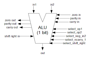
One bit of the ALU in the 8085 microprocessor.

One bit of the ALU in the 8085 microprocessor

The ALU has seven basic operations: or, add, xor, and, shift right, complement, and subtract. The following table shows the five control lines that select the operation, and the meaning of the carry line for the operation. Note that the meaning of carry in and carry out is different for each operations. For bit operations, the implementation of the ALU circuitry depends on a particular carry in value, even though carry is meaningless for these operations.

Operationselect_neg_in2select_op1select_op2select_shift_rightselect_ncarry_1Carry in/out
or000011
add01000/carry
xor010011
and011010
shift right001110
complement100011
subtract11000borrow

The eight-bit ALU is formed by linking eight single-bit ALUs as shown below. The high-order bit is on the left, and the low-order bit on the right, matching the layout in silicon. The carry, parity, and zero values propagate through each ALU to form the final values on the left. The right shift input is simply the bit from the right, with the exception of the topmost bit which uses a special shift right input. The auxiliary carry is simply the carry out of bit three. The control lines to select the operation are fed into all eight ALU slices. By combining eight of these ALU slices, the whole 8-bit ALU is created. The values from the top bit are used to control the parity, zero, carry, and sign flags (as well as the undocumented K and V flags). Bit 3 generates the half carry flag.

The 8-bit ALU in the 8085 is formed by combining eight 1-bit slices.

The 8-bit ALU in the 8085 is formed by combining eight 1-bit slices.

The control lines

The ALU uses 29 control lines that are generated by a PLA that activates the right control lines based on the opcode and the position in the instruction cycle. For reference, the following table lists the 29 ALU control lines and the instructions that affect them.
Control lineRelevant instructions
ad_latch_dbus, write_dbus_to_alu_tmp, /ad_dbus IN/LDA/LHLD
/ad_dbus ARHL/DAD/DSUB/LDHI/LDSI/RDEL
/alu/a_to_dbus all
/dbus_to_act ARHL/DAD/DSUB/LDHI/LDSI/RDEL
a_to_act ACI/ADC/ADD/ADI/ANA/ANI/CMP/CPI/ORA/ORI/RAL/RAR/RLC/RRC/SBB/SBI/SUB/SUI/XRA/XRI
0/fe_to_act all
sel_alu_a all
alu_to_a ACI/ADC/ADD/ADI/ANA/ANI/CMA/CMC/DAA/DCR/IN/INR/LDA/LDAX/MOV/MVI/ORA/ORI/POP/RAL/RAR/RIM/RLC/RRC/SBB/SBI/SIM/STC/SUB/SUI/XRA/XRI
/daa DAA
sel_0_fe DCR
store_v_flag ACI/ADC/ADD/ADI/ANA/ANI/ARHL/CMP/CPI/DAA/DCR/INR/ORA/ORI/RAL/RAR/RLC/RRC/SBB/SBI/SUB/SUI/XRA/XRI
select_shift_right ARHL/RAR/RRC
arith_to_flags ACI/ADC/ADD/ADI/ANA/ANI/CMP/CPI/DAA/DCR/DSUB/INR/ORA/ORI/SBB/SBI/SUB/SUI/XRA/XRI
bus_to_flags POP PSW
/zero_flag_combine DAD/DSUB
/flags_to_bus ACI/ADC/ADD/ADI/ANA/ANI/ARHL/CALL/CC/CM/CMA/CMC/CMP/CNC/CNZ/CP/CPE/CPI//CPO/CZ/DAA/DAD/DCR/DCX/DI/DSUB/EI/HLT/IN/INR/INX/JC/JK/JM/JMP/JNC/JNK/JNZ/JP/JPE/JPO/JZ/LDA/LDAX/LDHI/LDSI/LHLD/LHLX/LXI/MOV/MVI/NOP/ORA/ORI/OUT/PCHL/POP/PUSH/RAL/RAR/RC/RDEL/RET/RIM/RLC/RM/RNC/RNZ/RP/RPE/RPO/RRC/RST/RSTV/RZ/SBB/SBI/SHLD/SHLX/SIM/SPHL/STA/STAX/STC/SUB/SUI/XCHG/XRA/XRI/XTHL
shift_right_in_select ARHL
xor_carry_in ANA/ANI/ARHL/CMP/CPI/DCR/DSUB/INR/RAR/RRC/SBB/SBI/SUB/SUI
select_op2 ANA/ANI/ARHL/RAR/RRC
/use_latched_carry /rotate_carry LDHI/LDSI/RLC/RRC
/carry_in_0 0 except for ACI/ADC/DAD/DSUB/LDHI/LDSI/RAL/RDEL/RLC/SBB/SBI
select_op1 ACI/ADC/ADD/ADI/ANA/ANI/CMP/CPI/DAA/DAD/DCR/DSUB/INR/LDHI/LDSI/RAL/RDEL/RLC/SBB/SBI/SUB/SUI/XRA/XRI
select_ncarry_1 ACI/ADC/ADD/ADI/CMP/CPI/DAA/DAD/DCR/DSUB/INR/LDHI/LDSI/RAL/RDEL/RLC/SBB/SBI/SUB/SUI
In combination with first control line, write_dbus_to_alu_tmp ADC/ADD/ANA/CMA/CMC/CMP/DAA/DCR/INR/MOV/ORA/RAL/RAR/RIM/RLC/RRC/SBB/SIM/STC/SUB/XRA
select_neg_in2 CMA/CMP/CPI/DSUB/SBB/SBI/SUB/SUI
carry_to_k_flag DCX/INX
store_carry_flag ACI/ADC/ADD/ADI/ANA/ANI/ARHL/CMC/CMP/CPI/DAA/DAD/DSUB/ORA/ORI/RAL/RAR/RDEL/RLC/RRC/SBB/SBI/STC/SUB/SUI/XRA/XRI
xor_carry_result xor for ANA/ANI/CMC/CMP/CPI/DSUB/SBB/SBI/STC/SUB/SUI
/latch_carry use_carry_flag CMC/LDHI/LDSI

Conclusions

By reverse-engineering the 8085, we can see how the ALU actually works at the gate and silicon level. The ALU uses many standard techniques, but there are also some surprises and tricks. There are two registers (ACT and TMP) that are invisible to the programmer. You'd expect a direct path from the data bus to the accumulator, but instead the data passes through the ALU. The increment/decrement logic uses the unexpected constant 0xfe, and there are two totally different ways of performing increment/decrement. Several undocumented instructions perform ALU operations without involving the accumulator at all.

This information builds on the 8085 reverse-engineering done by the visual 6502 team. This team dissolves chips in acid to remove the packaging and then takes many close-up photographs of the die inside. Pavel Zima converted these photographs into mask layer images, generated a transistor net from the layers, and wrote a transistor-level 8085 simulator.

Four Rigol oscilloscope hacks with Python

A Rigol oscilloscope has a USB output, allowing you to control it with a computer and and perform additional processing externally. I was inspired by Cibo Mahto's article Controlling a Rigol oscilloscope using Linux and Python, and came up with some new Python oscilloscope hacks: super-zoomable graphs, generating a spectrogram, analyzing an IR signal, and dumping an oscilloscope trace as a WAV file. The key techniques I illustrate are connecting to the oscilloscope with Windows, accessing a megabyte of data with Long Memory, and performing analysis on the data.

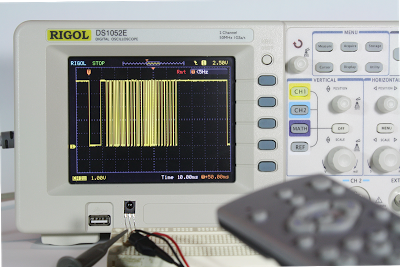
Analyzing the IR signal from a TV remote using an IR sensor and a Rigol DS1052E oscilloscope.

Analyzing the IR signal from a TV remote using an IR sensor and a Rigol DS1052E oscilloscope.

Super-zoomable graphs

One of the nice features of the Rigol is "Long Memory" - instead of downloading the 600-point trace that appears on the screen, you can record and access a high-resolution trace of 1 million points. In this hack, I show how you can display this data with Python, giving you a picture that you can easily zoom into with the mouse.

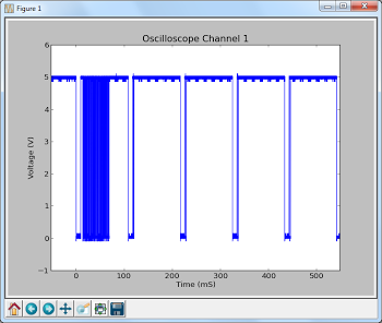
The following screenshot shows the data collected by hooking the oscilloscope up to an IR sensor. In the above picture, the sensor is the three-pin device below the screen. Since I've developed an IR library for Arduino, my examples focus on IR, but any sort of signal could be used. By enabling Long Memory, we can download not just the data on the screen, but 1 million data points, allowing us to zoom way, way in. The graph below shows what it sent when you press a button on the TV remote - the selected button transmits a code, followed by a periodic repeat signal as long as the button is held down.

The IR signal from a TV remote. The first block is the code, followed by period repeat signals while the button is held down.

The IR signal from a TV remote. The first block is the code, followed by period repeat signals while the button is held down.
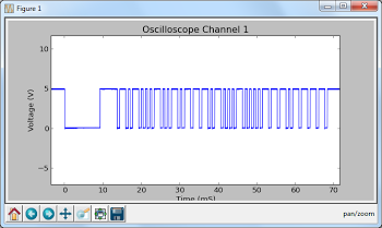
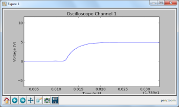
But with Long Memory, we can interactively zoom way on the waveform and see the actual structure of the code - long header pulses followed by a sequence of wide and narrow pulses that indicate the particular button. That's not the end of the zooming - we can zoom way in on an edge of a pulse and see the actual rise time of the signal over a few microseconds. You can do some pretty nice zooming when you have a million datapoints to plot.

Zooming in on the first part of the waveform shows the structure of the code - long header pulses followed by wide and narrow pulses. Zooming way, way in on the edge of a pulse shows the rise time of the signal.

To use this script, first enable Long Memory by going to Acquire: MemDepth. Next, set the trigger sweep to Single. Capture the desired waveform on the oscilloscope. Then run the Python script to upload the data to your computer, which will display a plot using matplotlib. To zoom, click the "+" icon at the bottom of the screen. This lets you pan back and forth through the data by holding down the left mouse button. You can zoom in and out by holding the right mouse button down and moving the mouse right or left. The magnifying glass icon lets you select a zoom rectangle with the mouse. You can zoom on your oscilloscope too, of course, but using a mouse and having labeled axes can be much more convenient.

A few things to notice about the code. The first few lines get the list of instruments connected to VISA and open the USB instrument (i.e. your oscilloscope). The timeout and chunk size need to be increased from the defaults to download the large amount of data without timeouts.

Next, ask_for_values gets various scale values from the oscilloscope so the axes can be labeled properly. By setting the mode to RAW we download the full dataset, not just what is visible on the screen. We get the raw data from channel 1 with :WAV:DATA? CHAN1. The first 10 bytes are a header and should be discarded. Next, the raw bytes are converted to numeric values with Mahto's formulas. Finally, matplotlib plots the data.

There are a couple "gotchas" with Long Memory. First, it only works reliably if you capture a single trace by setting the trigger sweep to "single". Second, downloading all this data over USB takes 10 seconds or so, which can be inconveniently slow.

Analyze an IR signal

Once we can download a signal from the oscilloscope, we can do more than just plot it - we can process and analyze it. In this hack, I decode the IR signal and print the corresponding hex value. Since it takes 10 seconds to download the signal, this isn't a practical way of using an IR remote for control. The point is to illustrate how you can perform logic analysis on the oscilloscope trace by using Python.

This code shows how the Python script can wait for the oscilloscope to be triggered and enter the STOP state. It also shows how you can use Python to initialize the oscilloscope to a desired configuration. The oscilloscope gets confused if you send too many commands at once, so I put a short delay between the commands.

Generate a spectrogram

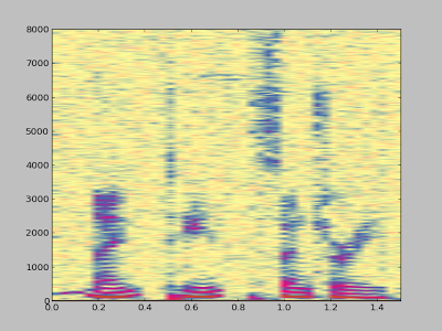
Another experiment I did was using Python libraries to generate a spectrogram of a signal recorded by the oscilloscope. I simply hooked a microphone to the oscilloscope, spoke a few words, and used the script below to analyze the signal. The spectrogram shows low frequencies at the bottom, high frequencies at the top, and time progresses left to right. This is basically a FFT swept through time.

A spectrogram generated by matplotlib using data from a Rigol DS1052E oscilloscope.

A spectrogram generated by matplotlib using data from a Rigol DS1052E oscilloscope.
To use this script, set up the oscilloscope for Long Memory as before, record the signal, and then run the script.

Dump data to a .wav file

You might want to analyze the oscilloscope trace with other tools, such as Audacity. By dumping the oscilloscope data into a WAV file, it can easily be read into other software. Or you can play the data and hear how it sounds.

To use this script, enable Long Memory as described above, capture the signal, and run the script. A file channel1.wav will be created.

How to install the necessary libraries

Before connecting your oscilloscope to your Windows computer, there are several software packages you'll need.
  • I assume you have Python already installed - I'm using 2.7.3.
  • Install NI-VISA Run-Time Engine 5.2. This is National Instruments Virtual Instrument Software Architecture, providing an interface to hardware test equipment.
  • Install PyVISA, the Python interface to VISA.
  • If you want to run the graphical programs, install Numpy and matplotlib.
You can also use Rigol's UltraScope for DS1000E software, but the included NI_VISA 4.3 software doesn't work with pyVisa - I ended up with VI_WARN_CONFIG_NLOADED errors. If you've already installed Ultrascope, you'll probably need to uninstall and reinstall NI_VISA.

If you're using Linux instead of Windows, see Mehta's article.

How to control and program the oscilloscope

Once the software is installed (below), connect the oscilloscope to the computer's USB port. Use the USB port on the back of the oscilloscope, not the flash drive port on the front panel.

Hopefully the code examples above are clear. First, the Python program must get the list of connected instruments from pyVisa and open the USB instrument, which will have a name like USB0::0x1AB1::0x0588::DS1ED141904883. Once the oscilloscope connection is open, you can use scope.write() to send a command to the oscilloscope, scope.ask() to send a command and read a result string, and scope.ask_for_values() to send a command and read a float back from the oscilloscope.

When the oscilloscope is under computer control, the screen shows Rmt and the front panel is non-responsive. The "Force" button will restore local control. Software can release the oscilloscope by sending the corresponding ":KEY:FORCE" command.

Error handling in pyVisa is minimal. If you send a bad command, it will hang and eventually timeout with VisaIOError: VI_ERROR_TMO: Timeout expired before operation completed.

The API to the oscilloscope is specified in the DS1000D/E Programming Guide. If you do any Rigol hacking, you'll definitely want to read this. Make sure you use the right programming guide for your oscilloscope model - other models have slightly different commands that seem plausible, but they will timeout if you try them.

Conclusions

Connecting an oscilloscope to a computer opens up many opportunities for processing the measurement data, and Python is a convenient language to do this. The Long Memory mode is especially useful, since it provides extremely detailed data samples.

Reverse-engineering the flag circuits in the 8085 processor

Processors all have status flags to keep track of conditions such as a zero value, a carry, or a negative value. Whenever you write a loop or conditional, these flags ultimately are in control. But how are these flags implemented in the chip's silicon? I've reverse-engineered the flag circuits in the 8085 microprocessor and explain what is really going on.

The photograph below is a highly magnified image of the 8085's silicon, showing the relevant parts of the chip. In the upper-left, the arithmetic logic unit (ALU) performs 8-bit arithmetic operations. The status flag circuitry is below the ALU and the flags are connected to the data bus (indicated in blue). To the right of the ALU, the control PLA decodes the instructions into control lines that control the operations of the ALU and flag circuits.

Photograph of the 8085 chip showing the location of the ALU, flags, and registers.

The 8085 has seven status flags.
  • Bit 7 is the sign flag, indicating a negative two's-complement value, which is simply a byte with the top bit set.
  • Bit 6 is the zero flag, indicating a value that is all zeros.
  • Bit 5 is the undocumented K (or X5) flag, indicating either a carry from the 16-bit incrementer/decrementer or the result of a signed comparison. See my article on the undocumented K and V flags.
  • Bit 4 is the auxiliary carry, indicating a carry out of the 4 low-order bits. This is typically used for BCD (binary-coded decimal) arithmetic.
  • Bit 3 is unused and set to 0. Interestingly, a fairly large transistor drives the data bus line to 0 when reading the flags, so this unused flag bit doesn't come for free.
  • Bit 2 is the parity flag, which is set if the result has an even number of 1 bits.
  • Bit 1 is the undocumented signed overflow flag V (details).
  • Bit 0 is the carry flag.

The image below zooms in on the flag silicon, showing individual transistors. The large transistors labeled with the flag name drive the flag value onto the data bus. From the data bus, the flag values control the results of conditional jumps, calls, and returns. The complex circuits above these transistors compute and store the flag values.

The silicon that implements the flags in the 8085 microprocessor.

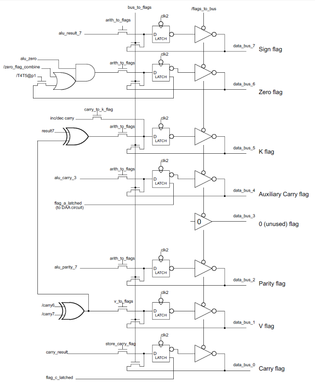
The schematic below shows the flag circuit that is implemented in the silicon above.

Schematic of the flag storage in the 8085 microprocessor.

Schematic of the flag storage in the 8085 microprocessor.

Each flag bit has a latch and control lines to write a value to the latch. Most flags are updated by the same arithmetic instructions and controlled by the arith_to_flags control line. The carry flag is affected by additional instructions and has its own control line. The undocumented K and V flags are updated in different circumstances and have their own control lines.

The bus_to_flags control loads the flags from the data bus for the POP PSW instruction, while the flags_to_bus control sends the flag values over the data bus for the PUSH PSW instruction or for conditional branches.

The circuitry to compute most flag values is straightforward. The sign flag is set based on bit 7 of the result. The auxiliary carry flag is set on the carry out of bit 3. The K and V flags are set based on the top two bits (details). The zero flag is normally set from the alu_zero signal that indicates all bits are zero.

The zero flag has support for multi-byte zero: at each step it can AND the existing zero flag with the current ALU zero value, so the zero flag will be set if both bytes are zero. This is only used for the (undocumented) DSUB 16-bit subtract instruction. Strangely, this circuit is also activated for the 16-bit DAD instructions, but the result is not stored in the flag.

If you look at the chip photograph at the top of the article, the flags are arranged in apparently-random order, not in their bit order as you might expect. Presumably the layout used is more efficient. Also notice that the carry flag C is off to the right of the ALU. Because of the complexity of the carry logic, which will be discussed next, the circuitry wouldn't fit under the ALU with the rest of the flag logic.

The carry logic

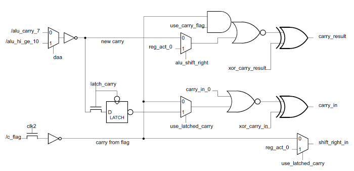
The schematic below shows the circuit for the carry flag. The logic for carry is more complex than for the other flags because carry is used in a variety of ways.

Schematic of the carry circuitry in the 8085 microprocessor.

Schematic of the carry circuitry in the 8085 microprocessor.

The value stored in the carry flag

The top part of the circuit computes carry_result, the value stored in the carry flag. This value has several different meanings depending on the instruction:
  • For arithmetic operations, the carry flag is loaded with the value generated by the ALU. That is, alu_carry_7 (the high-order carry from bit 7 of the ALU) is used. (See Inside the ALU of the 8085 microprocessor for details on how this is computed.)
  • For DAA (decimal adjust accumulator), the carry flag is set if the high-order digit is >= 10. This value is alu_hi_ge_10, which is selected by the daa control line.
  • For CMC (complement carry), the carry flag value is complemented. To compute this, the previous carry flag value c_flag is selected by use_carry_flag and complemented by the xor_carry_result control line.
  • For ARHL/RAR/RRC (rotate right operations), bit 0 of the rotated value goes into the carry. In the circuit, reg_act_0 (the low-order bit in the undocumented ACT (accumulator temp) register) is selected by the alu_shift_right control line.
The xor_carry_result control inverts the carry value in a few cases. For subtraction and comparison, it flips the carry bit to be the borrow bit. For STC (set carry), the xor_carry_result control forces the carry to 1. For AND operations, it forces the carry to 0.

Generating the carry input signal

The middle part of the circuit selects the appropriate carry_in value that is supplied to the ALU.
  • The first option is to set the carry in to either 0 or 1, by using carry_in_0 and optionally xor_carry_in. This is used for most instructions.
  • The next option is to use the current carry flag value as an input for additions or subtractions (allowing multi-byte arithmetic). For subtraction, this is inverted to convert borrow to carry; the xor_carry_in control does this.
  • The final option uses the carry latch to temporarily hold the carry for the undocumented LDHI and LDSI instructions. These instructions add a constant to a 16-bit register pair, so they need to add the carry from of the low-order sum to the high-order byte. The carry latch temporarily holds the carry, and this value is selected by the use_latched_carry control line. You might wonder why not just use the normal carry flag; the LDHI and LDSI instructions are designed to leave the carry flag unchanged, so they need somewhere else to temporarily store the carry. The surprising conclusion that Intel deliberately included circuitry in the 8085 specifically to support these undocumented instructions, and then decided not to support these instructions. (In contrast, the 6502's unsupported instructions are just random consequences of unsupported opcodes.)

    Generating the shift_right input signal

    Each bit of the ALU has a shift right input. For most of the bits, the input comes from the bit to the left, but the high-order bit uses different inputs depending on the instruction. The bottom circuit in the schematic below generates the shift right input for the ALU. This circuit has two simple options.
    • Normally the carry flag is fed into shift_right_in. For the ARHL and RAR instructions, this causes the carry flag to go into the high-order bit.
    • For the RRC and RLC instructions (rotate A left/right), the rotate_carry control selects bit 0 as the shift right input.

    Conclusions

    By reverse-engineering the 8085, we can see how the flag circuits in the 8085 actually works at the gate and silicon level. One interesting feature is the circuitry to implement undocumented instructions and flags. Another interesting feature is the complexity of the carry flag compared to the other flags.

    This information is based on the 8085 reverse-engineering done by the visual 6502 team. This team dissolves chips in acid to remove the packaging and then takes many close-up photographs of the die inside. Pavel Zima converted these photographs into mask layer images, generated a transistor net from the layers, and wrote a transistor-level 8085 simulator.

    Footnotes on rotate

    I recommend you skip this section, but there are few confusing things about the rotate logic that I wanted to write down.

    For some reason the rotate operations are named very strangely in the 8080 and 8085. RRC is the "rotate accumulator right" instruction and RAR is the "rotate accumulator right through carry" instruction. Based on the abbreviations, the names seem reversed. The left rotates RLC and RAL are similar. The Z-80 processor has a similar RRC instruction, but calls it "rotate right circular", making the abbreviation slightly less nonsensical.

    Bit 0 of ACT is fed into shift_right_in for both RRC and RLC. However, this input is just ignored for RLC since the rotation is the other direction, so I assume this is just a result of the control logic treating RRC and RLC the same.)

    To reduce the control circuitry, the rotate_carry and use_latched_carry control lines are actually the same control line since the instructions that use them don't conflict. In other words, there is just one control line, but it has two distinct functions.