JavaScript on the go: Programming from your phone

Have you ever wanted to write a program when the only computer available is your phone? You can use an Android phone to write and run JavaScript programs by using a few simple tricks.

While traveling over Thanksgiving I was thinking about how the 6502 microprocessor works and wanted to analyze some Boolean logic circuits. A trivial programming task but the only computer I had was my phone.

I searched for programming languages available on Android. Python for Android looked way too complex. The Clojure REPL intrigued me but I didn't want to learn Clojure right now. Other languages seemed limited or buggy. Then I was struck by the obvious choice for a powerful and fully-supported language with graphics capabilities: JavaScript. I could run JavaScript programs in the browser if I had a way to enter them.

I downloaded DroidEdit Pro which gave me a fullscreen editor for files on my phone. Typing HTML on the phone was painful until I downloaded the Hacker's Keyboard, which makes it much easier to type special characters. The picture below shows these tools in use.

My development cycle is:

  • Edit the code in DroidEdit and save it to a local .html file.
  • Select 'Preview in Browser' from DroidEdit and test the program.
  • Upload the file to my web server using DroidEdit's SFTP support when ready.

For debugging, the trick is to use the default browser, not Chrome. Enter about:debug in the URL bar to open the JavaScript console, which is vital for debugging.

Obviously this environment isn't as powerful as a full-size keyboard and monitor and powerful editor, but it lets me program no matter where I am. I haven't got the hang of cut-and-paste in the editor, but shift-arrow seems to work better than tapping.

Here's my program in action. It wont get any style points - I rapidly lost my enthusiasm for whitespace with the tiny keyboard - but it got the job done.

I also used this development environment to show my nephew how to make web pages with HTML. He thought it was very cool that he could type HTML into the phone, hit Control-S to save, and immediately load the web page on his iPad. He's now busily learning HTML and building his own web pages.

I hope these tips help you program while on the road. Leave a comment if you have tips of your own.

Teardown of the mysterious KMS 4-port USB charger

In this article I tear down a 4-port USB charger of puzzling origin. This charger is a huge step above the $2 counterfeit chargers I examined earlier in design and manufacture, but considerably below the quality of name-brand chargers. Likewise with safety - the charger was built with some attention to safety, but appears to fall short of UL standards.

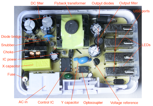
The circuit inside the KMS charger is a straightforward  flyback switching power supply. This photo shows the key components.

One puzzle about this charger is it's unclear who makes it and what model it is. The case says it's the KMS AC-09 but the circuit board says "TC09-new-V4.2". Amazon lists the brand as "Cosmos®", but I couldn't find any sign that KMS or Cosmos are actual companies. After some web searches, I think the charger is built by Guangzhou Panyu Qiaonan Saidi Electronic Factory (more) as the TC09 charger for $5.30 wholesale, or maybe HK Yingjia International, a consumer electronics manufacturer in Shenzhen (more). In any case, I'll call this the "KMS charger" since I need to call it something.

In my previous lab analysis of 12 chargers, I compared a dozen different chargers in 9 different categories, rating them from 1 to 5 'bolts' and the KMS charger came in about average in terms of performance. The results for the KMS charger are summarized below. For details on these measurements, see my previous article A dozen USB chargers in the lab).

Overall rating 3 out of 5
Vampire (idle) power usage 3 out of 5
Efficiency under load 3 out of 5
Achieves power rating 5 out of 5
Spikes in output 1 out of 5
High-frequency noise in output 4 out of 5
Ripple in output 5 out of 5
Voltage sag 1 out of 5
Current sag 1 out of 5
Regulation quality 1 out of 5

The good and the bad

Overall, this charger is much higher quality than the $2 counterfeit chargers, but considerably lower quality than name-brand chargers.

The charger provides more filtering than basic chargers, from the large input choke to the multiple output inductors. It includes X and Y capacitors for filtering.

The charger looks mostly safe, although it doesn't have UL certification and I suspect it would fail certification. The 6mm clearance between the primary and secondary looks solid. However, the transformer windings are only separated by 3mm, rather than 6mm, as I show below. (This is still much superior to the $2 chargers that have almost no separation.)

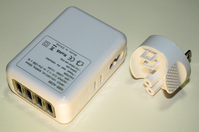
One interesting feature of the power supply is the power plug can be interchanged for use in different countries. (Some other chargers such as the HP TouchPad and Apple iPad are similar.)

The KMS TC-09 (AC09) 4-port USB charger. The power plug can be interchanged for use in different countries.

The charger has some quality issues. The power quality measurements I did in my previous article show the KMS charger has fairly poor quality output, with a lot of noise in the output.

The IC datasheet recommends 200 mm2 of foil on the IC output pins to provide cooling. I measured about 18 mm2 (less than 10% of recommended), which suggests the charger may overheat under full load.

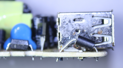
Some of the components in the KMS charger are mounted crooked, rather than flush with the circuit board. The inductor on the right and the optoisolator on the left are two examples.

The above photo shows that the build quality of the charger is not extremely high. The inductor at the front right is very crooked, and the optocoupler at the left is somewhat crooked. While this doesn't affect the performance, it shows the assembly was rapid rather than careful. More concerning, some of the solder joints appear to be almost bridged, which could cause catastrophic failure of the charger. I also found a government report of a KMS charger catching fire, apparently due to a loose wire in the power plug.

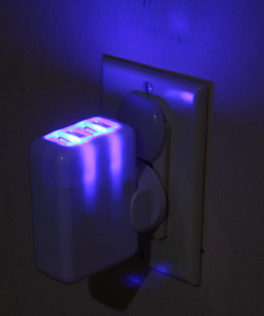
One unique feature of the charger is the blue LEDs which cause it to emit an eerie blue glow when in use. A lot of users dislike this though (according to reviews), because the light is distracting at night.

The KMS 4-port USB charger emits an eerie blue glow when in use.

The circuit

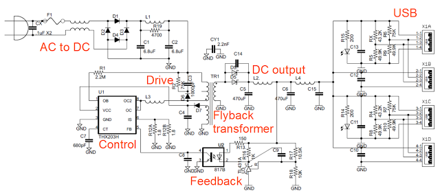
Annotated schematic of the KMS TC-09 USB charger.

For readers interested in circuits, I have prepared the above approximate schematic (click for a larger view). The circuit is pretty straightforward compared to other chargers (look at my iPhone charger schematic for comparison). Starting at the upper left, the input AC is converted to DC by the diode bridge, and then filtered by a simple inductor-capacitor filter. This high-voltage DC is connected to the flyback transformer primary. The THX203H control IC switches the other side of the flyback transformer to ground through the current-sense resistors R12A and R12B and inductor L3. (Most chargers use a separate switching transistor, but in this charger, the transistor is inside the control IC.) The snubber circuit R2, C3, and D6 absorbs some of the high-frequency switching spikes (although looking at the output below, this circuit isn't entirely successful). The auxiliary transformer winding and D7 and C4 provide the DC power to the control IC. The optocoupler provides feedback to the IC, indicating the output voltage level.

On the secondary side, the high-speed Schottky diodes (D5) convert the transformer output to DC. This is then filtered through an inductor-capacitor filter that smooths it out. The output voltage feedback is generated by the TL431A regulator and fed into the optocoupler.[1]

Finally, the actual USB output circuitry has more components than you'd expect. For each pair of ports, four resistors set the D+ and D- voltages to indicate to devices that the charger is (pretending to be) an Apple 2A charger. Each port has a small bypass capacitor to smooth out power transients. Finally there are two blue LEDs with current-limiting resistors to provide the blue glow.

The controller IC poses a bit of a mystery. It's labeled as the THX 203H controller, which turns out to be manufactured by NanJing TongHuaXin Electronic Co, Ltd., a Chinese switching power supply chip company (details). The datasheet for this part is very hard to understand, as it is machine-translated from Chinese, for example:

The startup circuit inside IC is designed as a particular current inhalation way, so it can start up with the magnification function of the power switch tube itself.
After some more investigation, this chip seems to be the SDC603 Current Mode PWM Controller designed by SDC Semi (Shaoxing Devechip Microelectronics Co., Ltd.). This is a Chinese state-level R&D center that is part of China's Torch Plan Project to develop high-tech industries. (Also check out the SDC company song.)

The controller chip is a basic 8-pin current-mode PWM controller chip. It includes a built-in NPN power transistor, which reduces the charger part count. The chip can produce 12 watts output power.

Circuit board

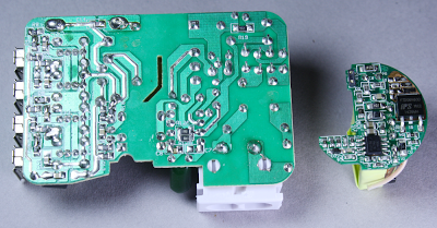
The circuit board from the KMS-AC09 charger on the left and a circuit board from the HP TouchPad charger on the right. Note the much higher density of the TouchPad board.

The above picture shows the KMS charger circuit board on the left and a circuit board from the HP TouchPad charger on the right. Compact phone chargers such as the iPhone or TouchPad chargers go to amazing effort to pack the components as tightly as possible. The KMS charger on the other hand has a much more spacious design with a lot of wasted space. Since any charger with 4 USB ports is going to be fairly large, they probably figured it's not worth the effort to make the rest of the circuitry compact. The difference in density between the two circuit boards is striking, though.

A key safety feature of the KMS charger is visible in the middle of the circuit board - note the angular cut-out slot, and the empty vertical region with no circuitry. This isolates the high-voltage circuits on the right from the low-voltage output circuits on the left. The KMS charger has a safe 6mm gap and the cut-out provides additional creepage distance. Counterfeit chargers usually skip this critical safety feature, with only a millimeter or two keeping the high voltage from reaching the output and shocking the user.

You might wonder how the charger works if the high voltage and low voltage circuits are separated by a gap. The key is that any components that cross this gap must be specially designed to avoid electrical hazards. The key component is the flyback transformer, which transfers the power through magnetic fields, avoiding any direct electrical connection between the two sides. The feedback signal passes from the secondary to the primary through an optocoupler, which transmits the feedback through a light signal, again avoiding an electrical connection. Finally, a Y safety capacitor connects the primary and secondary grounds to reduce electrical noise. The design of a Y capacitor ensures it won't pass dangerous electrical currents, and won't short out even under fault conditions.

Transformer teardown

The flyback transformer is the key component of a charger and usually the largest and most expensive. The transformer is where the high input voltage is converted to the output voltage, and the two voltages are in extremely close proximity, so the safety of the transformer is critical. From the outside, you can't tell if the manufacturer saved a few cents by leaving out most of the insulation, as happens with $2 chargers. I tore apart the transformer of the KMS charger to see what's inside.

The black circle on top of the transformer seen earlier is simply a foam disk, which helps reduce transformer noise by padding the transformer against the case. If a charger makes a high-pitched noise, it's usually coming from the transformer. Power supplies are usually designed with switching frequencies higher than people can hear, but in some circumstances it's still audible, especially if you are young and haven't lost high frequency hearing.

A copper 'belly band' provides a shield around the flyback transformer.

Under the first layers of insulating tape is a copper 'belly band' which surrounds the transformer to provide noise shielding from eddy currents in the transformer.[2] This copper shielding is omitted from super-cheap transformers, showing that this charger goes beyond the minimum.

The first winding in the flyback transformer powers the internal circuits of the charger

The windings are all separated by insulating tape. Under the belly band and insulating tape is the auxiliary winding, which provides power to the control IC. You might wonder why the IC needs a separate power supply instead of using the USB power output, but this wouldn't be safe because the USB output would no longer be isolated from the input. This winding is 9 turns of wire; since the IC requires low current, the wire is fairly thin.

The first half of the primary winding in the flyback transformer. Note the 3mm white boundary tape at the right that keeps the winding away from the edge.

Above you can see half of the primary winding, which is fed by the input power. This winding has 40 turns of wire.

An interesting safety feature is the 3 mm "margin tape"[3] to the lower right of the winding, which ensures that the primary winding stays 3 mm away from the edge. I was interested to see this, since other transformers I've disassembled use triple-insulated wire instead of boundary tape. To ensure safe electrical isolation between the primary and secondary windings, either the secondary wires need to be triple-insulated, or there needs to be at least 6mm of distance between the windings. Super-small chargers don't have 3mm of extra room, so they use the more expensive triple-insulated wire. But since the KMS is larger, it uses the 3mm margin tape. I'm not an expert on safety requirements, but it looks like this transformer doesn't quite meet the requirements. Normally, the margin tape is put on both sides, so there's a total of 6mm creepage distance between the windings.[4][5] But since the tape is only on one side, the windings only have half of the required distance.

To support high current, the secondary winding in the flyback transformer is four strands of thick wire. Note the 3mm white boundary tape at the right that keeps the winding away from the edge.

The secondary winding provides the low-voltage high-current output with 8 turns of wire. In order to support 2 amps, this winding has thick wire with four strands in parallel. I haven't seen parallel strands like this before, probably because the KMS charger supplies higher power. Note the 3mm margin tape keeping the winding away from the edge.

The second half of the primary winding in the flyback transformer. The 3mm boundary tape is clearly visible at the right.

Finally, the second half of the primary winding forms the innermost layer of the transformer; this is also 40 turns of wire. The primary winding is split into two layers that surround the secondary winding for better electrical properties. Note that the primary winding is 80 turns, while the secondary output winding is 8 turns. To oversimplify a bit, this means the output will be 10 times the current of the input at 1/10 the voltage, which is how the high voltage low current input results in the low voltage high current output. The above picture gives a good view of the 3mm margin tape at the right that keeps the wire away from the edge of the core.

Measuring the charger in use

The charger is a switching power supply using a flyback transformer. How this works is the high voltage DC is switched on and off tens of thousands of times a second by the control IC. These pulses of DC are sent into the flyback transformer. A flyback transformer is different from normal transformers in that the output diode blocks power from flowing out of the transformer while power is flowing in. Instead, as the current increases, power is stored in the transformer as a magnetic field. When the input current switches off, the stored power then flows out of the transformer, providing the desired output.

By looking at the output voltage and frequency spectrum, we can determine a fair bit about how the device operates. I measured a constant 60 kHz switching frequency above 1 amp output load, but a dropping frequency for lower loads. The datasheet gives some clues to this behavior. The power supply normally operates using PWM (pulse width modulation). The switching frequency is constant, but the amount of time the power transistor is on varies. The longer it is on, the more power into the transformer and the more output power. This matches the observed behavior from 1 amp to 3.5 amps. The datasheet also describes how the switching frequency drops under low power, which matches what I observed below 1 amp.

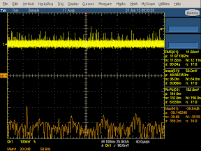
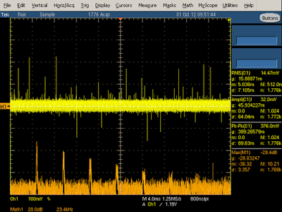
KMS charger output (yellow)and spectrum (orange) at 2A.  Note the spectrum peaks at 60.1 kHz and harmonics.

The above oscilloscope trace illustrates the behavior when producing 2 amps. The frequency spectrum shows narrow peaks (orange) at the 60 kHz switching frequency and harmonics. The yellow output voltage shows a bunch of large spikes due to the power switching on and off - this indicates that the charger isn't filtering the output very well, letting these spikes get into the connected device.

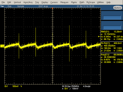
The diagram below zooms in to show the output in more detail. Each spike is when the switching transistor turns on at 60 kHz. The output power drops as the current through the flyback transformer increases (since the transformer secondary is blocked by the diode at this time). The output then climbs when the transistor switches off and the power is transferred to the secondary.

KMS charger output at 2A, showing the effect of the switching frequency.

As the charger load increases above 3 amps, the quality of the output significantly decreases, and large 120 Hz ripple appears in the output (yellow). This is probably because the input capacitors can't store enough power to provide a constant output at this high load. Since the charger is only rated to provide 2.1 amps of output, I don't consider this a design flaw, but it's interesting to see this behavior in the output. The key result here is not to overload the charger, because the power quality gets much worse.

KMS charger output (yellow)and spectrum (orange) at 3A.  The output contains a lot of 120 Hz ripple as well as switching spikes.

The charger is designed to reduce the switching frequency under low load for efficiency. I found this feature kicks in at loads under 1 amp, with the switching frequency smoothly dropping from 60 kHz to 29 kHz at 250 mA load and even lower under no load. The graph below shows the frequency spectrum at 250 mA load. Note that the spikes are wider than the previous case since the frequency becomes more unstable when it is reduced.

The frequency spectrum of the charger under lower (250 mA) load shows the reduced 29 kHz switching frequency and harmonics.

The output waveform below at 250 mA is similar to the previous (2A) case, except at a lower frequency. Note that the output still has large spikes when the transistor switches on. The output voltage drops while the switching transistor is on and then rises while the transistor is off (due to the flyback design), so you can see below that the transistor is off most of the time at low power.

The output waveform of the charger under low (250mA) load shows a lower 29 kHz switching frequency.

Power consumption

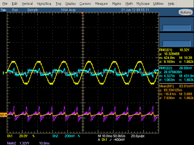
Measuring the power consumption of a charger is tricky because the charger doesn't use power like a normal resistive load, but uses a nonlinear part of the input current. This results in a power factor lower than unity. (You might expect that the poor power factor is because the charger switches on and off thousands of times a second, but actually it's the fault of the diode bridge.) I measured the power consumption of the charger under load by measuring the instantaneous line voltage and current, computing the instantaneous power, and then computing the real power from this.[6] In the following diagrams, the input line voltage is shown in yellow, and the input current is in cyan. The instantaneous power is graphed in orange at the bottom - simply the product of the voltage and current.[7]

The oscilloscope output below shows the power usage of the charger under no load. The line input voltage (yellow) is a nice sine wave, but the current (cyan) is very irregular. There is a bump corresponding to the voltage peaks as the input diodes conduct and re-charge the filter capacitors. The remaining current oscillations are unusual - I haven't seen them in other chargers, and I expect they are due to the large input choke. From the orange line you can see that the power usage has small spikes at 120 Hz. Taking the power factor into account and computing real power shows the charger uses 180 mW when idle which is fairly high, but actually lower than the Apple iPhone charger.

KMS charger line input under no load. Yellow is 120V input, cyan is input current. Bottom shows instantaneous power.

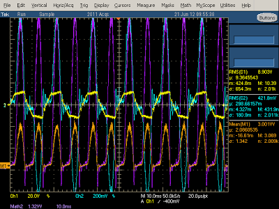
With load applied to the charger, the power usage shoots up as shown below. I compute the power usage as 6.4 watts, while the charger is supplying 4.4 watts to the output, for an efficiency of 69%. The shape of the current curve (cyan) and power curve (orange) shows that the charger is taking line power about half the time (the big curved peaks), and not for the other half (the flat oscillations in between). This illustrates the bad power factor that switching power supplies have. (PC power supplies often use power factor correction (PFC) circuits to improve the power factor.)The yellow input voltage curve is somewhat distorted, probably due to the lame isolation transformer I used.

KMS charger line input under load. Yellow is 120V input, cyan is input current.

You might wonder what happens if you short-circuit the output of the charger. It is designed to shut down before damage occurs, rather than self-destruct. After the internal voltage drops, the charger will start up again, and repeat this cycle until the problem goes away. This is called "hiccup mode", since the charger generates hiccups of power. The oscilloscope trace below shows the power consumption of the KMS charger when shorted. Note the pulses as it start up and shuts down every 250 milliseconds.

KMS charger line input under shorted load. Yellow is 120V input, cyan is input current. Bottom shows instantaneous power. Note the 'hiccup' shutdown and restart every 250 milliseconds.

Components

For those who are interested in the components, I have some details. The two 6.8uF 400V electrolytic capacitors in the primary are made by ChengX. The two 470uF capacitors in the secondary are made by JWCO. The X capacitor is a .1uF K 275V X2 made by Dain Electronics, a Chinese manufacturer of plastic metal film capacitors, now merged with WINDAY Electronic Industrial Co Ltd. The Y1 capacitor is a JN222M 2200pF disk ceramic suppression capacitor manufactured by Jya-Nay, a Taiwanese capacitor company. There's also a blue 681J (i.e. .68nF) polyester film capacitor of unknown manufacturer; looking at the circuit board this capacitor (C7) was originally a surface-mounted device, but was replaced with a larger capacitor.

The diodes are manufactured by MIC (Master Instrument Corporation, Shanghai). Most chargers use a diode bridge to convert the AC to DC, but this charger uses four independent diodes, which are 1N4007 700V diodes. The secondary rectification uses two Schottky diodes (SR360 3 amp 60V) from MIC. The circuit board uses the unusual mounting of two diodes on top of each other soldered into the same holes. The charger also uses FR107 700V fast recovery diodes.

Like most power supplies, the charger uses a TL431A for the voltage feedback.[1] This TL431A is produced by Wing Shing Computer Components The optocoupler is an ORPC 817B optocoupler from Shenzen Orient Technology Co., Ltd. (I don't want to speculate on the cultural significance of their raising the flag over Iwo Jima company logo.)

Conclusion

The KMS charger occupies an interesting middle ground between dangerous $2 counterfeit chargers and expensive name-brand chargers. Tearing down this 4-port USB charger of unknown origin reveals details of the circuitry. It also illustrates a network of Chinese suppliers and manufacturers, most of which are hardly known in the US. On Amazon, customer ratings for this charger are split between people who love it and people who hate it, which seems reasonable given what I saw in the teardown. Thanks to Gary F. for providing the charger.

Notes and references

[1] To summarize the feedback circuit: R17 and R18 form a resistor divider on the output voltage. If the output voltage is above 5.125 volts, the TL431 control input will be above 2.5 and the TL431 conducts. This energizes the optocoupler, providing current pulling the FB pin lower. Low FB increases the duty cycle, increasing the maximum transformer current, and increasing the output voltage. If the output voltage is considerably too high, or overtemperature is sensed, the switching frequency is decreased, reducing the power transferred to the output. (This is over-simplified; the frequency response of the feedback control loop is controlled via R13, R16, C8, and C9.) An alternative is to sense voltage from the primary side, so the feedback circuit can be eliminated. This reduces the total charger cost by about 20 cents according to a report.

[2] The use of a copper "belly band" in flyback transformers is discussed in Flyback Transformer Design for the UCC28600 (page 2). It provides an electromagnetic radiation shield. The article mentions that the belly band may cause difficulties with creepage requirements and that seems to be the case with the KMS, since there is only 3mm creepage between the primary-grounded belly band and the secondary wiring.

[3] A lot of interesting information about flyback transformer design and construction is in Cookbook for do-it-yourself transformer design

[4] A discussion of how to achieve 5-6mm creepage distance by using 2.5 or 3mm margin tape is in Flyback Transformer Design for the IRIS40xx Series. Note that the margin tape must be on both sides of the winding to achieve this distance, while the KMS transformer only uses the tape on one side.

[5] Safety Considerations in Power Supply Design provides a detailed explanation of safety requirements for power supplies. It explains creepage and clearance

[6] See Understanding power factor and input current harmonics in switched mode power supplies for details on power factor, power supplies have poor power factors, and why poor power factors are a bad thing. Briefly, the power factor is due to the non-linear current through the diodes at peaks, not due to a phase shift. Real power can be measured with an oscilloscope as the average value of the instantaneous power, see Power - Real And Apparent: A Tutorial On Basic Line Power Measurements or Measuring power using the DL750.

[7] For the input power measurements it is very important to use an isolation transformer to avoid destroying your oscilloscope or shocking yourself. For my measurements, a resistor voltage divider reduced the input line voltage - the actual voltage is 11.06 times the displayed probe 1 voltage (C1, yellow). The current was measured through a 5.2 ohm shunt resistor, so the current is 1/5.2 times the displayed probe 2 voltage (C2, cyan). Combining these, the power in watts is 2.13 times the measured C1*C2 value (M1, orange).

Obama on sorting 1M integers: Bubble sort the wrong way to go

Recently StackOverflow and Hacker News discussed the question of how to sort 1 million 8-digit numbers in 1 megabyte of RAM. This reminded me of when I saw Obama in 2007 at Google - Eric Schmidt asked Obama how to sort 1 million integers as a laugh line, but Obama shocked him by answering "I think the bubble sort would be the wrong way to go." The video is pretty entertaining:

Here's the transcript:

SCHMIDT: Now, Senator, you're here at Google and I like to think of the presidency as a job interview. Now, it's hard to get a job as president. And--I mean, you're going to do a great job. It's also hard to get a job at Google. We have questions and we ask our candidates questions. And this one is from Larry Schwimmer. What--you guys think I'm kidding, it's right here.[1] What is the most efficient way to sort a million 32-bit integers?

OBAMA: Well...

SCHMIDT: Maybe--I'm sorry...

OBAMA: No, no, no, no. I think--I think the bubble sort would be the wrong way to go.

SCHMIDT: [facepalm] Come on. Who told him this? Okay. I didn't see computer science in your background.

OBAMA: We've got our spies in there.[2]

If you're wondering about the complete answer to the sorting question, see a detailed explanation.[3]

All in all, it was a very unexpected answer from Obama with perfect delivery.

Notes

[1] Nervous laughter greeted the mention of a Larry Schwimmer question, because he once asked Jimmy Carter about his UFO encounter.

[2] Eric Schmidt had asked the sorting question to John McCain on a different visit, with the expected result. See the YouTube clip of McCain's visit.

[3] The pedantic may note that Obama's question is slightly different from the Stack Overflow question since it involves 32-bit integers vs. 8 digit integers, and the memory constraint was omitted.

How to create a new schematic symbol in the Eagle editor

This tutorial describes how to create a custom schematic symbol in the CadSoft Eagle editor. It assumes that you have some familiarity with Eagle and just want to create a schematic (not a PCB), but can't find a component you need.

Creating a part is surprisingly tricky - Eagle is one of those software packages with a GUI that looks more intuitive than it is. To create a component, there are three abstractions to deal with: Symbol, Package, and Device. The Symbol is the symbol as it appears in the schematic. It must be tied to a Package, which describes the shape of how the component is physically mounted on a circuit board, in particular the pads for the pins. Finally, the Device holds the complete description of a device, including the symbol and potentially multiple packages. Thus, even if you just want a schematic symbol, you must also deal with the package and device. The following image shows important parts of the Device screen.

The Device window in Eagle. The Symbol and Package are part of the Device.

Example: Zener diode

For example, suppose you want to create a Zener diode symbol by modifying one of the existing diode symbols.

First, find a part in an existing library you want to modify, e.g. use Edit > Add, then Search for something similar. Note the name of the library and the device, e.g. "diode" and "IN4004".

Next, create your custom library by going to the Control Panel and selecting File > New > Library, or open your existing library.

In Control Panel expand the library that has the component you want to copy and find the package you want. Right click and select "Copy to Library".

Next, open the new symbol in your library: Go to Library > Symbol and select the Symbol. Or from the Device screen right click on the crosshair in the middle of the symbol and select Edit Symbol.

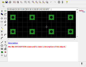
Finally, you can edit the symbol using the standard Eagle editor functions. To make a Zener diode, I needed to change the grid resolution to 0.025, select the angular wire bend, and then use Wire to add the "fins" to make the symbol look like a Zener diode.

Modifying an existing symbol to create a Zener diode in Eagle.

Go to File > Save As..., and save the new library.

To use this new library in your schematic, select Library > Use, and add your new library.

Improving the Symbol

The steps above are sufficient to edit and use a new component, but you may want to clean things up a bit.

To rename your symbol, go to Library > Rename, and enter a new name for the symbol.

To add a description, click on the Description link and enter a description using HTML. Typically it has <b>the title</b> <p>, and then a description.

To move the >NAME or >VALUE, use move and click on the crosshair at the lower left. You might want to temporarily reduce the grid size to get more control over the position.

Improving the Device

Go to Library > Device, and select the device.

To rename the device, use Library > Rename to rename the Device. You can also change the description as above, which is useful for searching.

To change the symbol's prefix (e.g. D1, D2, D3 for diodes), click on Prefix and enter the desired prefix.

You probably just want to have one package, so delete others by right clicking on them on the Device screen and selecting Delete.

To rename the package, go to Library > Package, and select the package. Then use Library > Rename to rename the Package. You can also change the description.

Adding new pins

If you want to add new pins to a symbol, things become more complicated, because you also need to add pads to the package and connect the pins to the pads, even if you don't care about PC boards. I recommend picking a starting symbol with the right number of pins if possible. But if not, use the following steps to add new pins.

Add the pins using Draw > Pin. You may need to rotate the pin. Right click the pin and select Properties to change the length or other property. You can enter a pin name or set Visible: Off if you don't want the pin name to show up.

To add pads, go to the Device, right click the Package, and select Edit Package. Add a Pad (anywhere) using the green circle icon.

Next you need to connect the pins and pads. Go to Library > Device and select your device. You will notice in the package pane an exclamation point in a circle. Underneath, click Connect, which will bring up the Connect panel. Select a Pin and a Pad and click Connect, until all pins are connected, and click Ok. Badk at the Device screen, you should now see a checkmark next to the Package. If you don't connect the pad to the pin, you will get "Error: Device ... has unconnected pin (G$1/P$1)!" when you try to add it to the schematic.

Creating an IC (or other component) from scratch

To create an IC, you can modify an existing IC device, a generic package from the ic-package library, or start from scratch. The existing devices are very function-specific and the ic-package symbols are kind of ugly, so you may end up needing to start from scratch. It's not too difficult and only takes a few minutes, but there are more steps than you might expect.

First, create a package with the right number of pins. Go to Library > Package, enter your package name (e.g. DIP8) after New, and click Ok. Using the green pad, drop 8 (for example) pads onto the package - the positions don't matter if you're not generating a PCB. Use Properties on each one (right click) to give the pads names 1, 2, etc.

A placeholder Package for an 8-pin IC in Eagle CAD.

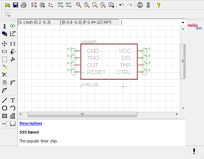
Go to Library > Symbol, enter your symbol name after New (e.g. 555), and click Ok. (For this example, I'll create a 555 timer from scratch even though the library has one.) Put down all the pins for your IC, leaving plenty of room horizontally for the labels, rotating the pins as necessary. Under properties, give each pin the desired name and set length to short. Use four wires to create the outline. Put Text >NAME on the name layer (95) and Text >VALUE on the value layer (96). Add a description if you want.

Creating a custom Symbol for an IC using Eagle CAD. The pins have been labeled.

Go to Library > Device, enter your device name after New (e.g. 555) and click Ok. Click on Add, select your new symbol, and add your symbol to the device. Under the package pane, click New, select your package, and click Ok. Click Connect, and carefully connect all the pins to the right pads, so the pin numbers show up okay. (Tip: do the pins in numerical order.) Click Ok. Add a Prefix and Description if you want.

Creating a new IC device in CadSoft Eagle. The Symbol and Package have been added to the Device.

Save your library with File > Save, and it should be ready to use.

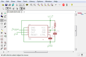
The new 555 IC symbol in use in an Eagle schematic.

Conclusion

CadSoft's Eagle PCB software is very useful for generating schematics, but the components you need are often missing. If you know the tricks, creating new symbols is not too hard, though. (If you want to create parts for a PCB, see Creating a new device in Eagle or Instructables or Sparkfun's tutorial.) I wrote this tutorial mainly for my own benefit, but I hope others find it useful too. Please leave a comment if you find errors or have additional suggestions.

Spectral analysis with the Tektronix 5000 oscilloscope

Many oscilloscopes have advanced spectral analysis features that perform Fourier Transforms on measured signals to generate a frequency spectrum. This article provides a tutorial on how to use these features on the Tektronix 5000 oscilloscope, assuming you already understand what a frequency spectrum is.

Getting started

The basic idea is you measure a waveform with the oscilloscope and use spectral analysis to see the frequency spectrum of this waveform. The first step is to display the desired input, which I assume you know how to do.

Next, to start Spectral analysis, go to Math -> Spectral Setup.... Choose Magnitude, Channel 1, and Ok. This will display the spectrum of channel 1 as the Math1 curve.

controls for spectral analysis

You'll discover there are a dozen settings with complex interactions. There are three columns of controls: Time Controls (Record Length, Sample Rate, Duration, and Resolution), Gating Controls (Gate Position, Gate Duration, and Gate Length), and Frequency Controls (Center Frequency, Frequency Span, and Resolution Bandwidth).

The Time Controls select how much data is collected. Record Length is the number of data points collected, Sample Rate is the sampling frequency, Duration is the time interval collected, and Resolution is the time between samples.

The Gating Controls select which data is actually used for the FFT, since you can use less data than you are collecting. Gate Duration is the sub-region of the Duration that is processed, and Gate Length is the number of samples in the Gate Duration. The Gate Duration is the interval between vertical yellow lines in the display.

The Frequency Controls select what results are displayed. The displayed frequency spectrum is centered on Center Frequency with total width of Frequency Span. Clicking Full will make the Frequency Span as large as possible with the existing settings. The Resolution Bandwidth specifies how detailed the frequency spectrum is, so smaller is "better".

Controlling the parameters

By clicking on a parameter, two of the parameters will be assigned to multi-function knobs, indicated by two circles next to the parameter and a green line indicating which knob controls it. Note that due to interdependencies between the parameters, adjusting one parameter can change other parameter. Also, the range of a parameter may be constrained by other parameters. You can also click on the number and manually entera value, or often set it to the minimum or maximum value, which can be convenient.

Advice

First figure out the maximum frequency you're interested in, the time period you're interested in, and the minimum frequency resolution you want.

Set the Sample Rate to at least twice the maximum frequency of interest. (Note that Sample Rate is basically in Hertz; s means samples per second, not seconds for Sample Rate. Resolution is the reciprocal of Sample Rate.)

Duration controls the Resolution Bandwidth; a longer Duration yields a smaller (better) Resolution Bandwidth. At least two cycles of the lowest frequency of interest must fit into the Duration. The Duration should include several cycles of the waveform of interest. Note that if the Duration is multiple seconds, it will inconveniently take a long time to collect data before showing you the waveform. And if the Record Length is long, the processing time will be long.

The Record Length will be determined from the Sample Rate and Duration, Generally around 20,000 is a good value. A much smaller value won't give you good frequency resolution, and a much larger value will slow down processing.

The Resolution control is usually the best Time control to adjust, since the others interact with each other in annoying ways.

For the Gating controls, I recommend leaving the Window Type at Gaussian and the Gate Position at 0 unless you know you want to do something else. you probably want the Gate Duration to be as large as the Duration, or else you're wasting data and getting a worse Resolution Bandwidth. If the Gate Duration is smaller than the Duration, it will be displayed as vertical yellow lines that show the part of the waveform that is getting processed.

For the Frequency Controls, you probably want Center Frequency to be half of Frequency Span; this means that you're seeing the full spectrum starting at 0. It's very easy for Center Frequency to get larger, which means you're looking at a random region in the middle of the middle of the spectrum, so you may need to continually set the Center Frequency back to the minimum value. It usually works best to modify freqency by increasing the Frequency Span and decreasing the Center Frequency, to keep the two in sync. If the frequency spectrum looks like sine waves rather than spikes, the Resolution Bandwidth is probably too large.

Be careful you don't clip the input waveform on the top of the screen, as this will mess up the spectrum. Set the vertical scale so it fits.

Example: Square wave frequency spectrum

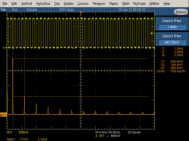
An easy example is to generate the frequency spectrum of the 1kHz calibration square wave. (Just connect the probe to the calibration output on the oscilloscope.) The theoretical spectrum for a square wave is spikes for the odd harmonics, with height proportional to 1/n. Specifically, a 1 volt peak-to-peak square wave will have harmonics of 2/π/n volts peak-to-peak for odd n, or 0.63V and 0.21V for the first two (odd) harmonics. Converting the harmonics to RMS voltages by dividing by sqrt(2) yields theoretical RMS voltages of 0.450V and 0.150V for the first two harmonics.

frequency spectrum of square wave

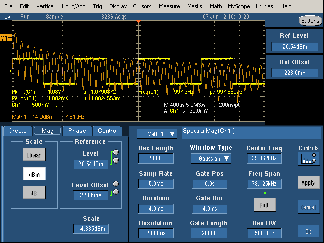
The above picture shows a first attempt at generating the frequency spectrum (orange) of the square wave (yellow). The duration is too short - it only includes 4 cycles of the waveform, so the Resolution Bandwidth is large (500Hz). The result is the spikes are spread out into sine-like curves and the spectrum is not very distinct.

square wave spectrum showing large frequency span

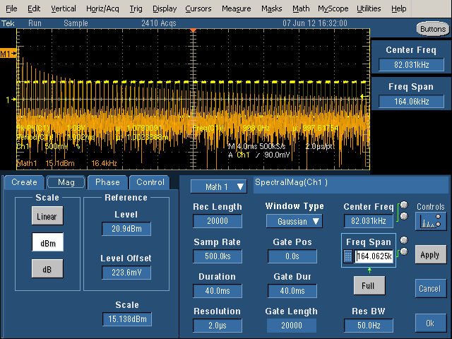
In the above picture, the duration has been increased to 40mS, so 40 cycles of the waveform are included. With a long duration, the Resolution Bandwidth is narrow (50Hz), so the harmonics are narrow spikes as desired. However, with a wide Frequency Span, the harmonics are crammed together and hard to see.

spectrum zoomed in with decreased frequency span

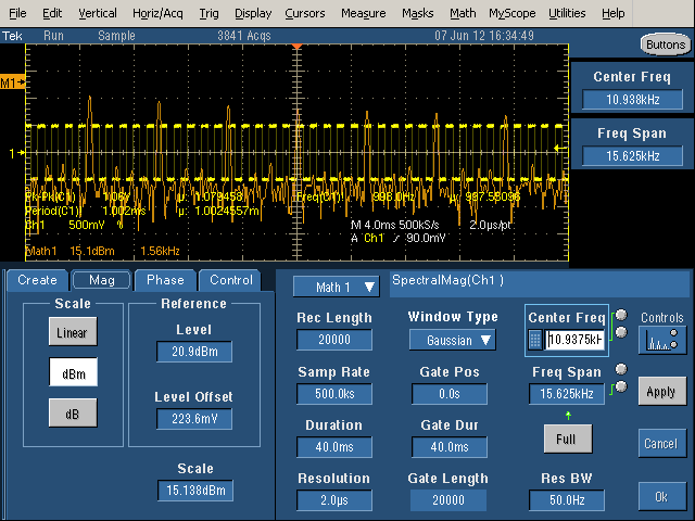
To see the spectrum in more detail (zoomed-in), decrease the Frequency Span, which gives more detail of the spectrum. However, note that the spikes are all almost the same size. since the Center Frequency is not half of the Frequency Span, we're looking at the middle of spectrum (3.125kHz to 18.75kHz), rather than starting at 0Hz. It is very easy to accidentally shift the spectrum range and get confused about what you're seeing, so be cautious.

spectrum of square wave

Finally, with the Center Frequency set to half of the Frequency Span, the image above shows the spectrum starting at 0. The frequency scale (Math1) is 1.56kHz per grid line, so the spikes are at 1kHz, 3kHz, 5kHz, etc. as expected. (Inconveniently, I can't find a way to get the frequency scale to be round numbers.)

spectral analysis showing Gate Duration

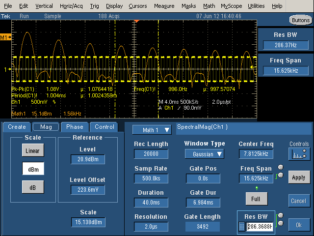
With the Gate Duration decreased, note the vertical yellow lines showing the gate region. Only the signal between the lines is being processed. This increases the Resolution Bandwidth (i.e. makes it worse), so the harmonics are now considerably wider than the spikes seen previously.

The theory behind dB and dBm

The dB and dBm scales are logarithmic, which allows harmonics with a large range of powers to be displayed: when the power increases by a factor of 10, the dB measurement increases by 10 dB. dB is measured against an arbitrary reference power, so the fomula is dB = 10 * log10(power / powerreference). Since the oscilloscope measures voltage, not power, the fomula actually used is dB = 20 * log(V / Voffset), for a fixed offset voltage. Voffset corresponds to 0 dB. Since power is proportional to V^2, increasing the voltage by a factor of 10 increases the power by a factor of 100 which increases the dB value by 20 dB.

For the dBm scale, the offset voltage is set to 223.6mV. Although this value may seem random, there is an explanation. The definition of dBm is 10*log(power), where power is the RMS power in milliwatts. dBm is defined with a fixed impedance of 50Ω. (Other fields use different impedances for dBm, for example audio work uses 600Ω.) Working through some math yields Vref = sqrt(50Ω*1mW) = 223.6mV. (See Wikipedia for more explanation of dBm.)

The oscilloscope's dB and dBm settings

On the oscilloscope, the Spectral controls affecting the dB display are Level, Offset, and Scale. Scale is the number of dB per division. Level controls the position of the M1 zero dB position, measured in dB below the top of the screen. Finally, Offset defines what voltage is 0 dB. The default Offset is 223.6 mV as explained above. Increasing Offset shifts the spectrum down with respect to the M1 zero position. For instance, Offset of 707.09 mV shifts the curve down by 10 dB, and 2.236V shifts the curve down 20 dB.

The scale values for Math1 are used to display the dBm curve. The vertical scale shows the number of dBm per division, and the horizontal scale shows the frequency per division. The M1 indicator on the left shows the position of 0 dBM. Note that dBm values can be positive or negative.

In the Math controls, the controls are Pos and Scale - Pos is the number of divisions that M1 (0 dBm) is above the center line, so Level = (4 - pos) * Scale.

On the oscilloscope, there are few differences between the dB and dBm settings. dBm defaults to centering the spectrum on the screen (which generally puts M1 high up), and using 223.6mV as the offset. dB defaults to centering M1 on the screen (which generally puts the spectrum lower). If you adjust the Level, Offset, and Scale to be equal, the dBm and dB settings give the same results, so they aren't fundamentally different. The default Level and Scale are usually ugly numbers; you can adjust them to round values.

The square wave spectrum gives an example of dBm in use. Looking at the theoretical values for the square wave, the first harmonic of 0.45V is 20*log(450mV/223.6mV) = 6.1dBm and the second odd harmonic of 0.15V is 20*log(150mV/223.6mV) is -3.5dBm. Looking at the measured harmonics, the first is about 0.4 divisions above the M1 mark, and the second is about 0.2 divisions below the mark. Since the scale is 15.1dBM / division, this yields measured values of 6dBm and -3dBm, close to the theoretical values.

Understanding the linear scale

spectral analysis showing linear scale

The linear scale displays the RMS voltage of each harmonic. The M1 arrow at the left indicates the 0 position (which can be adjusted). The Math1 Scale shows how many mV per vertical division, and how many kiloHertz per horizontal division. Position shows the number of divisions M1 is above the center line.

Changing the scale to Linear shows how the harmonics in the example drop off rapidly as 1/N: 1, 1/3, 1/5, 1/7, etc. (Note that higher-order harmonics are much harder to see with the linear scale than with the dB scale.) Aligning cursors with the first two harmonics indicate the first harmonic is 1kHz at 445.4mV, and the third harmonic is 3kHz at 144.6mV. These values are close to the theoretical values of 450mV and 150mV. The values can also be determined from the display using the scale. In this example, the Math1 scale is 117mV per vertical division and 2.5kHz per horizontal division. The first harmonic is about 3.8 divisions above the 0 level, which works out to 445mV.

Reading voltage and frequency values can be inconvenient because the scale usually ends up with inconveniently non-round values per division. Using a math cursor, as above, make this easier. The cursors are accessed under Cursors > Cursor Setup, and then moved to the desired positions.

Some relations between the controls

Many of the control values are related to other values by simple equations. The following relationships may help understand the controls.
  • 1 / Sample Rate = Resolution.
    Resolution is just the time between samples.
  • Record Length = Sample Rate * Duration.
    Record Length is the total number of samples collected.
  • Gate Length = Gate Duration * Sample Rate.
    Gate Length is the total number of samples processed.
  • Gate Duration ≤ Duration.
    The Gate Duration must be smaller than the total Duration.
  • Gate Length ≤ Record Length.
    The Gate Length must be smaller than the total Length.
  • Center Frequency ≥ Frequency Span / 2.
    The minimum frequency in the range must be positive.
  • Resolution Bandwidth = 2 / Gate Duration.
    The slowest waveform must fit into the duration at least twice.
  • Freq Span ≤ Sample Rate / 2.
    The Nyquist limit requires at least two samples at the highest frequency.
  • Spectral Level = (4 - Math Pos) * Scale
    Level is measured from the top of the screen, 4 divisions above the center line.

For the official Tektronix documentation, see Defining a Speactral Math Waveform in the TDS5000B Series Oscilloscopes Online Help, page 291. Also see TDS5000B Series Quick Start User Manual, page 75.

This tutorial is mostly for my own reference, so I can remember how to use the oscilloscope in the future, but hopefully it will be of benefit to some other readers.

A dozen USB chargers in the lab: Apple is very good, but not quite the best

When you buy a USB charger, how do you know if you're getting a safe, high-quality charger for your money? You can't tell from the outside if a charger provides silky-smooth power or if it is a dangerous charger that emits noisy power that cause touchscreen malfunctions[1] and could self-destruct. In this article, I carefully measure the performance of a dozen different chargers, rate their performance in multiple categories, and determine the winners and losers.
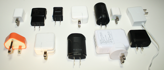
The above picture shows the twelve chargers I analyzed.[2] The charger in the upper-left is the cube-shaped Apple iPhone charger. Next is an oblong Samsung adapter and a cube Samsung adapter. The Apple iPad power adapter is substantially larger[3] than the iPhone charger but provides twice the power. The HP TouchPad power charger has an unusual cylindrical shape. Next is a counterfeit iPhone charger, which appears identical to the real thing but only costs a couple dollars. In the upper right, the Monoprice iPhone charger has a 30-pin dock connector, not USB. The colorful orange charger is a counterfeit of the Apple UK iPhone charger. Next is a counterfeit iPad charger that looks just like the real one. The Belkin power adapter is oval shaped. The KMS power supply provides four USB ports. The final charger is a Motorola Charger.

Summary of ratings

The chargers are rated from 1 to 5 energy bolts, with 5 bolts the best. The overall rating below is the average of the ratings in nine different categories, based on my measurements of efficiency, power stability, power quality, and power output. The quick summary is that phone manufacturers provide pretty good chargers, the aftermarket chargers are worse, and $2 counterfeit chargers are pretty much junk. Much to my surprise, the HP TouchPad charger (which isn't sold any more) turned out to have the best overall score. The counterfeit iPhone charger set a new low for bad quality, strikingly worse than the other two counterfeits.

 ModelOverall rating
Apple iPhone Apple A1265
Samsung oblong Samsung travel adapter ETA0U60JBE
Samsung cube Samsung travel adapter ETA0U80JBE
Apple iPad Apple 10W USB Power Adapter A1357
HP TouchPad Hewlett Packard LPS AC/DC Adaptor P/N 157-10157-00
Counterfeit iPhone Fake Apple A1265 "Designed by California"
Monoprice Monoprice Switching Mode Power Supply MIPTC1A
Counterfeit UK Fake Apple A1299
Counterfeit iPad Fake Apple 10W USB Power Adapter A1357
Belkin Belkin UTC001
KMS KMS-AC09
Motorola Motorola AC Power Supply DC4050US0301

Inside a charger

These chargers cram a lot of complex circuitry into a small package, as you can see from the iPhone charger below. (See my iPhone charger teardown for more details.) The small size makes it challenging to make an efficient, high-quality charger, while the commoditization of chargers and the demand for low prices pressure manufacturers to make the circuit as simple as possible and exclude expensive components, even if the power quality is worse. The result is a wide variation in the quality of the chargers, most of which is invisible to the user, who may believe "a charger is a charger".
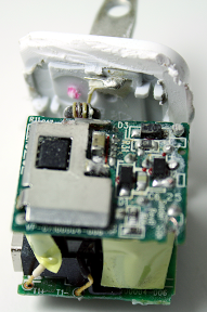
The circuitry inside the Apple iPhone USB charger

Inside the iPhone charger

Internally a charger is an amazingly compact switching power supply that efficiently converts line AC into 5 volt DC output. The input AC is first converted to high-voltage DC. The DC is chopped up tens of thousands of times a second and fed into a tiny flyback transformer. The output of the transformer is converted to low-voltage DC, filtered, and provided as the 5 volt output through the USB port. A feedback mechanism regulates the chopping frequency to keep the output voltage stable. Name-brand chargers use a specialized control IC to run the charger, while cheap chargers cut corners by replacing the IC with a cheap, low-quality feedback circuit.[4]

A poor design can suffer several problems. If the output voltage is not filtered well, there will be noise and spikes due to the high-frequency switching. At extreme levels this could damage your phone, but the most common symptom is the touchscreen doesn't work while the charger is plugged in.[1] A second problem is the output voltage can be affected by the AC input, causing 120 Hz "ripple".[5] Third, the charger is supposed to provide a constant voltage. A poor design can cause the voltage to sag as the load increases. Your phone will take longer to charge if the charger doesn't provide enough power. Finally, USB chargers are not all interchangeable; the wrong type of charger may not work with your device.[6]

Counterfeits

Counterfeit chargers pose a safety hazard as well as a hazard to your phone. You can buy a charger that looks just like an Apple charger for about $2, but the charger is nothing like an Apple charger internally. The power is extremely bad quality (as I will show below). But more importantly, these chargers ignore safety standards. Since chargers have hundreds of volts internally, there's a big risk if a charger doesn't have proper insulation. You're putting your phone, and more importantly yourself, at risk if you use one of these chargers. I did a teardown of a counterfeit charger, which shows the differences in detail.

I've taken apart several counterfeit chargers and readers have sent me photos of others. Surprisingly, the counterfeit chargers I've examined all use different circuitry internally. If you get a counterfeit, it could be worse or better than what I've seen.

How do you tell if a charger is counterfeit? The fakes are very similar; it's hard for me to tell, even after studying many chargers. There's a video on how to distinguish real and fake chargers through subtle differences. You can also weigh the charger (if you have an accurate scale), and compare with the weights I give above. The easiest way to get a genuine Apple charger is fork over $29 to an Apple store. If you buy a $2 "Original Genuine Apple" charger on eBay shipped from China, I can guarantee it's counterfeit. On the other hand, I've succeeded in buying genuine used chargers from US resellers for a moderate price on eBay, but you're taking a chance.

The following picture shows a counterfeit charger that burned up. The safety issues with counterfeits are not just theoretical; when hundreds of volts short out, the results can be spectacular.
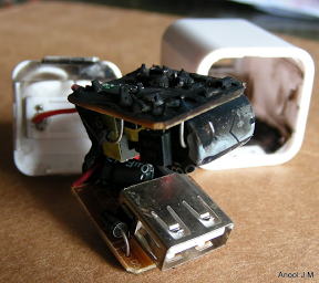
Counterfeit iPhone charger that burned up

Photo by Anool Mahidharia. Used with permission

Indicated charger type

A device being charged can detect what type of charger is being used through specific voltages on the USB data pins.[6] Because of this, some devices only work with their own special chargers. For instance, an "incorrect" charger may be rejected by an iPhone 3GS or later with the message "Charging is not supported with this accessory".[7]

There are many different charger types, but only a few are used in the chargers I examined. A USB charger that follows the standard is known as a "dedicated USB charger". However, some manufacturers (such as Apple, Sony, and HP) don't follow the USB standard but implement their own proprietary charger types. Apple has separate charger types for 1 amp (iPhone) and 2 amp (iPad) chargers. HP has a special type for the HP TouchPad.

The point is that USB chargers are not interchangeable, and devices may not work if the charger type doesn't match what the device expects. The table below shows the type of charger, the current that the label claims the charger provides, the current it actually provides, and the charger type it indicates to the device.

The types of the counterfeit chargers are a mess, as they advertise one power level, actually supply a different power level, and have the charger type for a third level. For example, the counterfeit iPhone charger is advertised as supplying 1 amp, but has the 2A charger type, so an iPad will expect 2 amps but not obtain enough power. On the other hand, the counterfeit iPad charger claims to supply 2 amps, but really only supplies 1 amp and has a 1A type.

 Charger typeLabelMeasured currentWeight
Apple iPhone Apple 1A charger5V 1A1.79A23.0g
Samsung oblong dedicated USB charger5V 0.7A.80A33.1g
Samsung cube dedicated USB charger5V 1A1.17A23.2g
Apple iPad Apple 2A charger5.1V 2.1A2.3A67.5g
HP TouchPad HP TouchPad charger5.3V 2.0A2.4A54.8g
Counterfeit iPhone Apple 2A charger5V 1A.94A18.8g
Monoprice Apple dock5V 1A1.22A67.8g
Counterfeit UK dedicated USB charger5V 1A.57A29.4g
Counterfeit iPad Apple 1A charger5.1V 2.1A1.2A43.4g
Belkin Apple 1A charger5V 1A1.27A43.0g
KMS Apple 2A charger5V 2.1A3.4A99.5g
Motorola dedicated USB charger5.1V .85A.82A38.6g

Efficiency

People often wonder how much power their charger is wasting while it's idle, and if they should unplug their charger when not in use. I measured this "vampire" power usage and found the chargers varied by more than a factor of 20 in their idle power usage. The Samsung oblong charger came in best, using just 19 mW; this was so low compared to the other chargers that I measured it again a different way to make sure I hadn't made an error. On the other extreme, the fake iPhone charger used 375 mW. The Apple iPhone charger performed surprisingly badly at 195 mW. If plugged in for a year, this would cost you about 21 cents in electricity, so it's probably not worth worrying about.[8] In the following table, I use the official charger Star Rating System (yes, there actually is such a thing).[9][10]

I also measured efficiency of the chargers under load.[11] One of the benefits of switching power supplies over simpler linear supplies is they are much more efficient at converting the input power to output. The chargers I measured all did pretty well, with 63% to 80% efficiency. The HP charger was the winner here.

 VampiremilliwattsEfficiencyPercent
Apple iPhone 19574
Samsung oblong 1976
Samsung cube 8677
Apple iPad 6278
HP TouchPad 9180
Counterfeit iPhone 37563
Monoprice 7872
Counterfeit UK 10363
Counterfeit iPad 9566
Belkin 23466
KMS 17969
Motorola 5975

The chargers up close

Apple iPhone and counterfeit
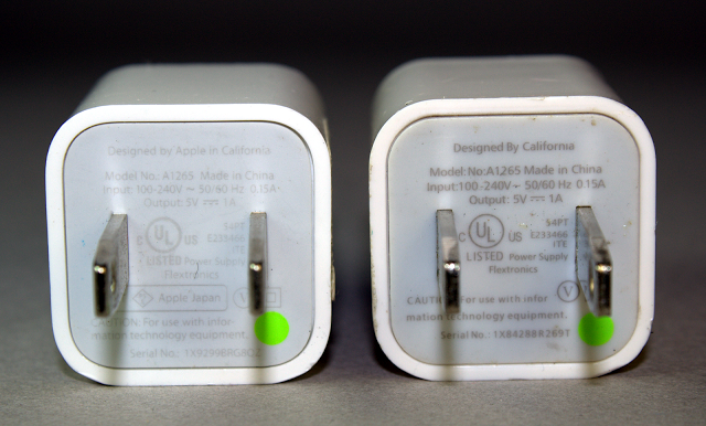
A real Apple iPhone charger (left) and a counterfeit charger (right

The above photo shows a real iPhone charger (left) and a counterfeit (right); the two chargers are almost identical, down to the green dot. If you look closely, the genuine one says "Designed by Apple in California", while the counterfeit has the puzzling text "Designed by California". The counterfeit also removed the "Apple Japan" text below the plug. I've seen another counterfeit that says "Designed by Abble" (not Apple). I assume the word "Apple" is removed for legal or trademark reasons, since the word "Apple" is often (but not always) missing from counterfeits.

Samsung oblong
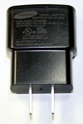
The Samsung oblong charger.

I call this charger the Samsung oblong charger, to distinguish it from the Samsung cube charger.

Samsung cube
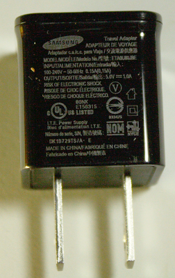
The Samsung cube charger is shaped very similarly to the Apple iPhone charger. Internally, however, it turns out to be entirely different.

Apple iPad and counterfeit
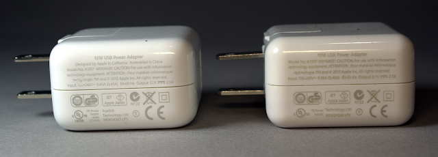
A real Apple iPad charger (left) and a counterfeit charger (right

The photo above shows a real iPad charger (left) and a counterfeit (right). The counterfeit has almost identical text, but without "Designed by Apple in California. Assembled in China", "Listed" under UL, and the manufacturer "Foxlink". Inexplicably this sanitization left "TM and © 2010 Apple Inc".
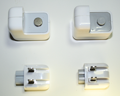
Real (left) and counterfeit (right) iPad chargers

The above photo shows a real iPad charger on the left and a fake iPad charger on the right, with the plug removed. The most visible difference is the real charger has a round metal grounding post, while the fake has plastic. (The US plug isn't grounded, but in other countries the lack of ground in the counterfeit could pose a safety hazard.)

HP TouchPad
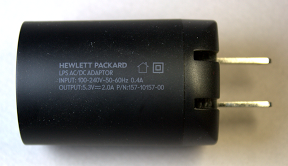
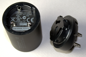
HP TouchPad charger HP TouchPad charger

The HP TouchPad charger has a very unusual cylindrical shape, which is striking if perhaps not practical. The charger twists apart, allowing the plug to be replaced for different countries. (It took me weeks to discover this feature.)

Monoprice
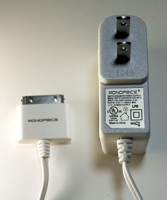
Monoprice USB charger

The Monoprice charger isn't a USB charger, but instead has a 30-pin iPhone dock connector attached. It is a relatively large charger.

Counterfeit UK
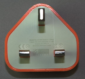
Counterfeit Apple UK iPhone charger

This charger is a counterfeit of the Apple UK iPhone charger. They've removed Apple from the text, but left Emerson Network Power, which I'm sure is not the actual manufacturer. The genuine Apple UK charger can be distinguished by a serial number inside the USB connector.

Belkin
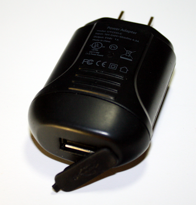
Belkin phone charger

The Belkin charger eschews the minimal design styling of most chargers, with a roughly oval cross section, curves and ribs, and a cover over the USB port.

KMS
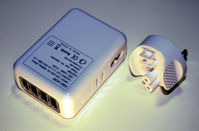
KMS 4-port USB charger with plug detached

The KMS charger is unusual in providing 4 USB ports. It also gives off a blue glow while in use. The plug can be removed and replaced for use in different countries, similar to the iPad and HP TouchPad chargers. I couldn't find any UL safety approval on this charger, but I did find a report of one catching fire.

Motorola
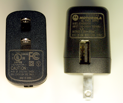
Motorola phone charger

The Motorola charger has the lowest listed power output, 850mA. The back of it has a holographic sticker (like a credit card), which may ward off counterfeiters, even though it's unlikely for anyone to counterfeit this charger. I wonder though why Apple doesn't use holograms or other anti-counterfeiting techniques, given the large number of counterfeit Apple chargers being sold.

Delivery of advertised power

Each charger has an advertised power output, but some chargers produce considerably more and some produce much less. Your device will take longer to charge, if the charger can't put out enough power. This table shows each charger's ability to deliver the rated power, based on my measurements of maximum power. While most chargers meet or exceed the power rating, there are some exceptions.

The counterfeit chargers perform extremely poorly, putting out a fraction of the expected power. Charging your device with one of these chargers will be a slow, frustrating experience. In particular, the counterfeit UK charger only produces a third of the expected power. Although the label claims the charger works on 100-240 volts, it's clearly not designed to work on US power.

The iPad is a surprise, putting out less power than expected. Despite being nominally a 10 watt charger, the label says it provides 5.1V and 2.1A, which works out to 10.7 watts. However, the maximum power I measured is 10.1 watts (4.4 volts at 2.3 amps, as shown in the Power section below). Since the measured power is slightly less than advertised, it only gets four bolts.

 RatingLabelWatts from labelMeasured watts
Apple iPhone 5V 1A5.06.0
Samsung oblong 5V 0.7A3.54.0
Samsung cube 5V 1A5.05.5
Apple iPad 5.1V 2.1A10.710.1
HP TouchPad 5.3V 2.0A10.611.4
Counterfeit iPhone 5V 1A5.02.7
Monoprice 5V 1A5.05.7
Counterfeit UK 5V 1A5.01.7
Counterfeit iPad 5.1V 2.1A10.75.9
Belkin 5V 1A5.05.6
KMS 5V 2.1A10.510.9
Motorola 5.1V .85A4.34.3

Power quality

In this section, I measure the quality of the power produced by the different chargers. I analyze it for voltage spikes, high frequency noise, and line-frequency ripple. The following table summarizes the results in three categories. Spikes indicates extremely brief large voltage spikes in the output, while Noise indicates high-frequency noise in the output, and Ripple indicates low-frequency (120 Hz) fluctuations in the output.[12]

 SpikesNoiseRipple
Apple iPhone
Samsung oblong
Samsung cube
Apple iPad
HP TouchPad
Counterfeit iPhone
Monoprice
Counterfeit UK
Counterfeit iPad
Belkin
KMS
Motorola

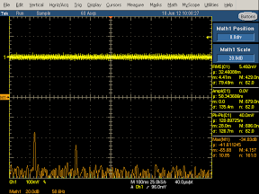
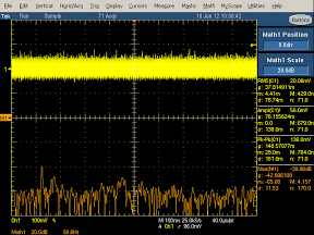
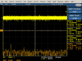
The following oscilloscope traces show the output signal (yellow) and frequency spectrum (orange). The left images provide high-frequency information on the output voltage. The right images show the low-frequency information on the output voltage.[13]

The desired voltage graph is a flat, thin yellow line indicating totally smooth power. However, some factors mess this up. First, any ripple from the power line will show up as 5 sinusoidal peaks in the first (high-frequency) yellow line. High-frequency noise will widen the yellow line. Voltage spikes will appear as vertical spikes in the yellow line.

The plots also show the frequency spectrum in orange, from 0 at the left to 230 kHz at the right. The desired graph would have the orange spectrum near the bottom of the screen. Thus, the power quality exponentially gets worse as the orange line gets higher. The left (high frequency) spectrum generally shows noise at the switching frequency of the charger (and harmonics). The right (low frequency) spectrum typically shows spikes at multiples of 120 Hz, caused by ripple from the 60 Hz power.[5]

Apple iPhone
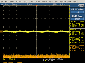
High frequency oscilloscope trace from Apple iPhone charger Low frequency oscilloscope trace from Apple iPhone charger

The ripple is clearly visible as the waves in the yellow trace on the left and as the spikes (at 120 Hz and 240 Hz) in the orange trace on the right.

The iPhone charger performs extremely well at filtering out spikes and noise, the best of the chargers I measured. Apart from the 120 Hz spikes, the noise spectrum (orange) is flat and very low. The power quality is so good, I checked the results several times to make sure I wasn't missing something.

Samsung oblong
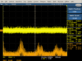
High frequency oscilloscope trace from Samsung oblong charger Low frequency oscilloscope trace from Samsung oblong charger

The Samsung charger's output has a lot more noise than the iPhone charger. This is visible in the thickness and jaggedness of the yellow output curves. The orange frequency spectrum on the left shows large peaks at harmonics of the switching frequency. The 120 Hz spike on the right is a bit lower than the iPhone charger, so the ripple filtering is a bit better.

Samsung cube
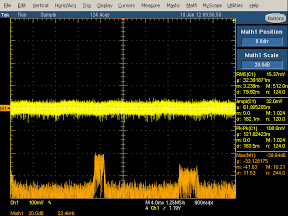
High frequency oscilloscope trace from Samsung cube charger Low frequency oscilloscope trace from Samsung cube charger

The Samsung cube charger shows some noise in the output (yellow). The frequency spectrum shows wide peaks at multiples of the the switching frequency, about 90kHz. There's some ripple.

Apple iPad

High frequency oscilloscope trace from Apple iPad charger Low frequency oscilloscope trace from Apple iPad charger

The iPad charger almost eliminates the ripple; only a small blip is visible in the orange spectrum on the right. The noise level is low, although appreciably worse than the iPhone.

HP TouchPad
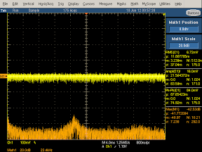
High frequency oscilloscope trace from HP TouchPad charger Low frequency oscilloscope trace from HP TouchPad charger

There's no ripple visible in the HP charger spectrum on the right. The overall noise level is good.

Counterfeit iPhone
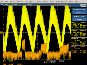
High frequency oscilloscope trace from counterfeit iPhone charger Low frequency oscilloscope trace from counterfeit iPhone charger

The output from this counterfeit charger is a wall of noise. In order to fit the waveform in the display, I had to double the scale on the left and increase it by a factor of 5 on the right, so the yellow curve is actually much worse than it appears. On the left, note the huge ripple with massive high-frequency noise on top. This output is not something you want to feed into your phone.

Monoprice
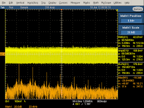
High frequency oscilloscope trace from Monoprice USB charger Low frequency oscilloscope trace from Monoprice USB charger

The output from this charger is very noisy, as you can see from the thickness of the yellow line. Note that the frequency spectrum (left) has very tall but narrow spikes at harmonics of the 28kHz switching frequency, showing a lot of high-frequency noise. On the positive side, there is hardly any ripple.

Counterfeit UK
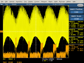
High frequency oscilloscope trace from counterfeit UK iPhone charger Low frequency oscilloscope trace from counterfeit UK iPhone charger

This charger has very bad output. The large degree of ripple is visible in the waveform (yellow, left) and the very large spikes in the spectrum (orange, right). The thickness of the yellow waveform shows the large amount of high-frequency noise, which is also visible in the very high peaks in the spectrum (orange, left).

Counterfeit iPad
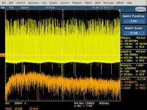
High frequency oscilloscope trace from counterfeit iPad charger Low frequency oscilloscope trace from counterfeit iPad charger

This counterfeit charger has so much noise in the output that I had to double the scale on the left to get it to fit. Note the very large spikes in the output (yellow). The spectrum (orange, left) is much higher everywhere, indicating noise at all frequencies. Surprisingly, it has only a moderate amount of ripple; the manufacturer seems to have done at least one thing right.

Belkin
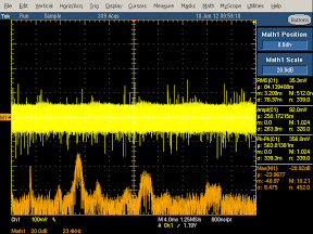
High frequency oscilloscope trace from Belkin phone charger Low frequency oscilloscope trace from Belkin phone charger

The Belkin charger does well at eliminating ripple, but has a lot of noise otherwise. The spectrum (orange, left) shows large peaks. The yellow output is wide, showing a lot of noise, combined with many large voltage spikes of about 1/3 volt.

KMS
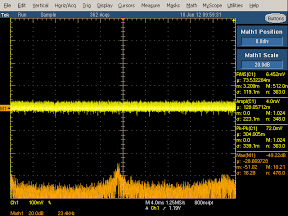
High frequency oscilloscope trace from KMS charger Low frequency oscilloscope trace from KMS charger

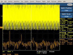
The KMS charger has fairly good output, with a small peak in the spectrum (orange, left) at the switching frequency. It has no detectable ripple. However, it has many large voltage spikes in the output, over half a volt, as can be seen on the right.

Motorola
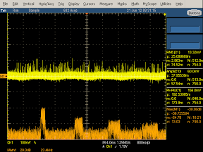
High frequency oscilloscope trace from Motorola phone charger Low frequency oscilloscope trace from Motorola phone charger

The Motorola charger has a lot of spikes in the output (yellow) . The spectrum (orange, left) shows high frequency noise at the switching frequencies. There's a moderate amount of ripple (yellow, left and orange, right).

Summary

The quality of the output power is radically different between chargers. The counterfeit chargers are uniformly bad, with hardly any effort at filtering the output. The other chargers vary in quality with the iPhone charger setting the standard for noise-free power, but surprisingly poor filtering of ripple. The power quality is a key factor that affects the performance of chargers; spikes and noise are known to interfere with touchscreens.[1]

Power curve

In this section I look at the voltage and current output by the charger as the load increases. The first rating is Voltage Sag, which is the undesired drop in output voltage as the load increases. The second rating is Current Sag, which shows how the current fluctuates as load increases. Finally, Regulation shows the overall stability of the output from the charger.
 Voltage sagCurrent sagRegulation
Apple iPhone
Samsung oblong
Samsung cube
Apple iPad
HP TouchPad
Counterfeit iPhone
Monoprice
Counterfeit UK
Counterfeit iPad
Belkin
KMS
Motorola

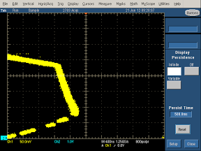
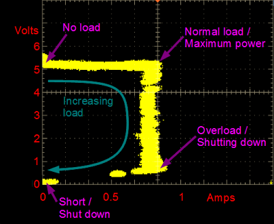
The graphs in this section need a bit of explanation, which is provided in the diagram below. The voltage/current load curve shows the performance of the charger under different loads. Each point on the curve shows the current (X axis) and voltage (Y axis) produced by the charger under a particular load condition. Follow the yellow curve clockwise from the upper left to the lower left to see the effect of increasing load. The upper left point of the curve shows the voltage produced by the charger when there is no load on the charger. As the load increases, the charger is supposed to keep a constant voltage and increase the current (i.e. horizontal line), until it reaches the maximum power (upper right). If the load continues increasing, the charger switches to a constant current mode, dropping the voltage while continuing to provide the maximum current (i.e. vertical line).[14] At the lower right, the charger has reached its shutdown point due to excessive load, and rapidly drops to no output in the lower left corner to avoid damage.
Example Voltage vs Current graph for a phone charger

[16]

Apple iPhone

Voltage vs Current curve for Apple iPhone charger

The output from the Apple iPhone charger is surprisingly non-constant under load. The charger starts off with 5.2 volts with no load, dropping to 4.6 volts as the load increases, resulting in the downwards slope of the top yellow line. As the load increases, the current keeps increasing, resulting in the slope of the right yellow line. Note however that the yellow line is relatively thin, so the regulation is pretty good at each point.

Note that because this charger has a high current output, this chart has a different current (horizontal) scale than most of the charts to fit the whole trace in the image. Stretch it horizontally to compare with other graphs.

Samsung oblong
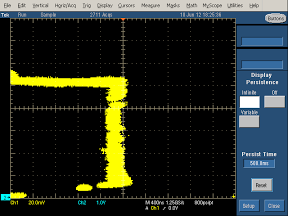
Voltage vs Current curve for Samsung oblong charger

For this charger, the voltage is approximately flat, except for a bump under no load (upper left) which is probably a measurement artifact. The vertical yellow line shows the current stays nearly constant as the load increases. The charger shows good voltage and current stability under changing load. The yellow line is a bit wider than the iPhone charger, showing a bit less regulation for a fixed load.

Samsung cube
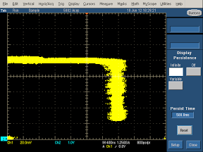
Voltage vs Current curve for Samsung cube charger

The voltage curve sags slightly under load. The right hand curve shows the current stays stable, but the line is moderately wide, showing a bit of weakness in regulation.

Apple iPad
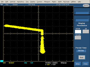
Voltage vs Current curve for Apple iPad charger

Similar to the iPhone charger, the iPad charger shows a lot of voltage sag. The voltage is about 5.1 V unloaded, dropping to 4.4 volts and 2.3 A (10.1 W) at the corner. Unlike the iPhone charger, the iPad charger has pretty good current stability. The regulation is solid, as shown by the narrowness of the yellow trace. Note the scale change due to the high current output.

I'm puzzled by the steep voltage sag on both the iPhone and iPad charger. Since the designers of the Apple charger went to a great deal of effort to build a high quality charger, I conclude they must not consider voltage sag worth worrying about. Or, more interestingly, maybe they built this sag as a feature for some reason. In any case, the chargers lose points on this.

HP TouchPad
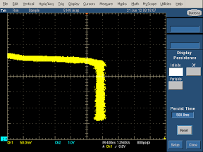
Voltage vs Current curve for HP TouchPad charger

The charger has some voltage sag, but the current (vertical) is nice and constant. The yellow line is relatively thin, showing good regulation. Note the scale change due to the high current output.

Counterfeit iPhone
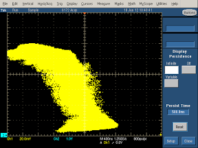
Voltage vs Current curve for counterfeit iPhone charger

This counterfeit charger shows extremely poor regulation, as shown by the very wide yellow line. It's hard to fit a voltage-current curve to this picture. The amount of power supplied by this charger seems almost random.

Monoprice
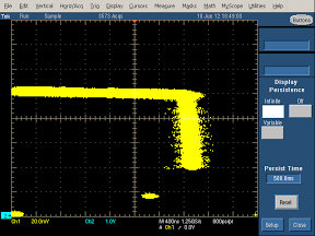
Voltage vs Current curve for Monoprice charger

The Monoprice charger shows reasonably straight voltage and current lines showing good constant voltage and current outputs. The vertical line shows some width and noise, suggesting the regulation isn't totally stable.

Counterfeit UK
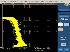
Voltage vs Current curve for counterfeit UK iPhone charger

For this charger, the upper line doesn't get very far, showing that this charger doesn't output much current. My suspicion is that it was only tested with 240 volts so it performs poorly with 120 volts, even though the label says it takes 100 to 240 volts. The width of the yellow line shows very poor regulation.

Counterfeit iPad
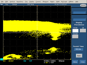
The output of this counterfeit charger is so poorly regulated that it's hard to tell exactly what's happening with the voltage and current. It looks like the voltage is roughly constant underneath all the noise.

Belkin
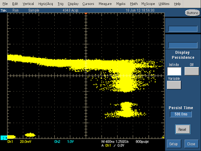
Voltage vs Current curve for Belkin phone charger

The Belkin charger shows voltage sag as the current increases. In addition, the output is fairly noisy.

KMS
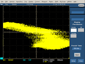
Voltage vs Current curve for KNS phone charger

The KMS charger shows a lot of voltage sag as the load increases. In addition, the output is all over the place, showing very poor regulation, more like what I'd expect from a counterfeit charger. Note the scale change due to the high current output.

Motorola
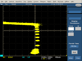
Voltage vs Current curve for Motorola phone charger

The Motorola charger shows a bit of voltage sag, but good current stability. The regulation is good but not perfect, as shown by the width of the yellow line. (The gaps in the vertical line are just measurement artifacts.) Note that the maximum current output of this charger is fairly low (as advertised).

Conclusions

So what charger should you spend your hard-earned money on? First, make sure the charger will work with your phone - for instance, newer iPhones only work with certain chargers. Second, don't buy a counterfeit charger; the price is great, but it's not worth risking your expensive device or your safety. Beyond that, it's your decision on how much quality is worth versus price, and I hope the data here helps you make a decision.

P.S. How about some teardowns?

My previous iPhone charger and fake charger teardowns were surprisingly popular, but if you were hoping for teardowns on the full set of chargers, you'll need to wait for a future blog post. I haven't torn the chargers apart yet; if I need to take more measurements, I don't want to have just a pile of parts. But I do have some preview pictures to hold you over until my teardown article.
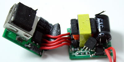
Counterfeit Apple iPhone charger internals

The above picture shows the internals of a counterfeit Apple iPhone cube charger. The two boards stack to form the compact cube shape. This charger blatantly tries to pass as a genuine Apple charger; unlike the "Designed by California" charger, this one exactly copies the "Designed by Apple in California" text from the real charger. Note the very simple circuitry[4] - there are no components on the other side of the board, no controller IC, and very little filtering. Also look at the terrible mounting of the transistor on the front right; clearly the build quality of this charger is poor. Finally, note the overall lack of insulation; this charger wouldn't meet UL safety standards and could easily short out. But on the plus side, this charger only cost a couple dollars.
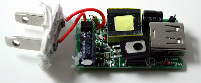
Inside a cheap USB charger

The above $2 charger is notable for its low-profile design; it's about as thin as you can make a charger and still fit the power prongs and the USB port. The transformer is very short to fit into this charger. Like the previous charger, it uses a very simple circuit,[4] has little filtering, and almost no safety insulation.
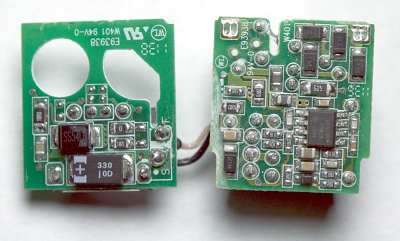
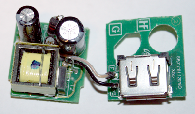
The complex circuit inside a Samsung cube USB charger Circuit boards of a Samsung cube USB charger, showing the transformer, switching transistor, filter capacitors, and other large components

Finally, the above pictures show the internals of the Samsung cube charger, which has circuit boards packed with tiny components and is much more advanced than the counterfeits (although slightly less complex than the Apple charger). Despite being very similar to the Apple charger on the outside, the Samsung charger uses an entirely different design and circuitry internally. One interesting design feature is the filter capacitors fit through the cut-out holes in the secondary circuit board, allowing the large filter capacitors to fit in the charger.

More comments on this article are at Hacker News and reddit. Thanks for visiting!

Notes and references

[1] For an explanation of how the noisy output from cheap chargers messes up touchscreens, see Noise Wars: Projected Capacitance Strikes Back.

[2] The charger selection may seem slightly eccentric; it is based on chargers I had previously acquired, chargers I could obtain at a reasonable price, chargers supplied by Gary F. and Anthony H. (thanks, guys!), and some counterfeit chargers for comparison.

[3] TI has an interesting new design for a 10 watt inch-cube charger. With this design a tablet charger could be as small as the iPhone charger.
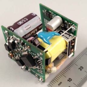
Texas Instruments PMP8286 10W cube charger.

Photo of PMP8286 10W cube charger used with permission from Texas Instruments.

[4] The cheap chargers all use a "ringing choke converter" circuit, which coincidentally is the same power supply topology used by the Apple II. These chargers use an extremely simple feedback mechanism in place of the control IC in higher-quality chargers. See a comic-book explanation or a technical explanation for details.

[5] Since the input AC has a frequency of 60 Hertz, you might wonder why the ripple in the output is 120 Hertz. The diode bridge converts the 60 Hz AC input to 120 Hz pulsed DC, as shown in the diagram below. The pulses are smoothed out with filter capacitors before being fed into the switching circuit, but if the filtering isn't sufficient the output may show some 120 Hz ripple.

Image by WdWd, used under CC BY 3.0

[6] The chargers use specific voltages on the data pins to indicate the charger type to the device being charged. Because of this, an "incorrect" charger may be rejected by an iPhone with the message "Charging is not supported with this accessory".[7] Under the USB standard, a charger should short the two data pins together to indicate that it's a "dedicated" charger and not a real USB device. However, companies such as Apple, HP, and Sony have their own proprietary nonstandard techniques. The following table summarizes the voltages that appear on the D+ and D- lines for different chargers, and how the D+ and D- lines are configured internally.

Charger typeD+ voltageD- voltageD+/D- shortedD+ pullup (kΩ)D+ pulldown (kΩ)D- pullup (kΩ)D- pulldown (kΩ)
dedicated USBfloatfloatyesnonenonenonenone
Apple .5A22no7549.97549.9
Apple 1A22.7no7549.943.249.9
Apple 2A2.72no43.249.97549.9
HP TouchPad 2A2.82.7yes250300n/an/a
Sony3.33.3no5.1105.110

Most of this data is based on Maxim USB Battery Charger Detectors, Adafruit's The mysteries of Apple device charging, TouchPad's USB Cable, XDA forum (Samsung), and TPS2511 USB Dedicated Charging Port Controller and Current Limiting Power Switch datasheet. The Apple 2A (i.e. iPad) information is a new result from my measurements. For details on USB charging protocols, see my references in my earlier posting.

Amusingly, semiconductor manufacturers have recently introduced chips that allow chargers to sequentially pretend to be different proprietary chargers until they trick the device into accepting the charger. It seems crazy that companies (such as Apple) design incompatible chargers, and then chip companies invent schemes to work around these incompatibilities in order to build universally compatible chargers. Two example chips are the TI TPS 2511 chip, and SMSC's USC1001 controller, which pretends to be nine different charger types.

[7] If you've wondered why some chargers cause the iPhone to give a "Charging not supported with this accessory" error, Silicon based annoyance reduction made easy describes how devices use proprietary protocols to limit the chargers they will work with.

[8] For the efficiency analysis I use 12 cents / kilowatt-hour as a typical residential energy price, which I got from US Energy Information Administration table 5.3.

[9] The official no-load charger star ratings are discussed at Meeting 30 mW standby in mobile phone chargers.

[10] There are many standards for energy consumption; see 5 W Cellular Phone CCCV (Constant Current Constant Voltage) AC-DC Adapter. For Energy Star ratings, a 5W charger must have under .5W no-load consumption, and 63% efficiency under load. A 10W charger must have under .75W no-load consumption, and 70% efficiency.

[11] Because switching power supplies use power in irregular waveforms, I used a complex setup to measure power consumption. I measured the AC input voltage and current with an oscilloscope. The oscilloscope's math functions multiplied the voltage and current at each instant to compute the instantaneous power, and then computed the average power over time. For safety and to avoid vaporizing the oscilloscope I used an isolation transformer. My measurements are fairly close to Apple's[15], which is reassuring.

You might wonder why I didn't just use a Kill A Watt power monitor, which performs the same instantaneous voltage * current process internally. Unfortunately it doesn't have the resolution for the small power consumptions I'm measuring: it reports 0.3W for the Apple iPhone charger, and 0.0W for many of the others. Ironically, after computing these detailed power measurements, I simply measured the input current with a multimeter, multiplied by 115 volts, and got almost exactly the same results for vampire power.

[12] The spike, noise, and ripple measurements come from the oscilloscope traces. The Spikes measurement is based on the maximum peak-to-peak voltage on the high frequency trace (the low frequency trace yields almost identical results). The Noise measurement is based on the RMS voltage on the high-frequency trace, and Ripple is based on the maximum dB measured in the low-frequency spectrum. These measurements appear on the right in the traces.

[13] In the power quality section, the high-frequency (left) images show 40 milliseconds of the waveform in yellow, and the frequency spectrum up to 234 kHz in orange. The low-frequency (right) images show 1 second of the output voltage in yellow and the frequency spectrum up to 600 Hz in orange. Because the frequency spectrum is measured in dBm, it is logarithmic; every division higher indicates 20 dB which is 10 times the voltage and 100 times the power.

[14] The chargers use a design called constant-voltage, constant-current (CVCC), since they provide a constant voltage (and increasing current) up to the maximum load and then a constant current (and decreasing voltage) if the load continues to increase. [15] The Apple 3GS Environmental Report gives some efficiency measurements for the Apple USB Power Adapter. It lists 0.23W no-load power and 75% efficiency. These values are reasonably close to my measurements of 0.195W no-load consumption and 73.6% efficiency.

[16] Measuring these curves was a bit tricky. I used a NTE2382 power MOSFET transistor as a variable load, manually varying the gate bias to generate the load curve. The transistor needed a large heat sink to dissipate 10 watts. A more complex dynamic load circuit is described here, but the simple circuit was sufficient for me.

The graphs were generated using the X-Y mode on the oscilloscope, with the load voltage as Y and the current as X. I used a .12Ω current sense resistor to measure the load current. This works out to 1/6 amp load current per division for the 20mV/div traces (most of them), and 5/12 amp load current per division for the 50mV/div traces (the high-current devices).

Note that increasing load corresponds to a decreasing resistance across the output: the upper left has infinite resistance (no load), the lower left has zero resistance (short circuit), and the resistance decreases in between. Since the power (in watts) is voltage * current, the maximum power is in the upper right corner, approximately 4W in this case. The load resistance can be computed by Ohm's law, e.g. middle of the upper curve: 5 V / .4 A = 12.5Ω, upper right corner 5 V / .8 A = 6.25 ohms. Middle of the right hand curve: 2.5 V / .8 A = 3Ω, overload point = .5 V / .8 A = .6Ω.

[17] Most of these chargers aren't made by the companies that sell them, and there are some interesting facts about the manufacturers. The manufacturers of the chargers can be looked up from the UL certification number. The oblong Samsung is made in China by Korean RFTech, a manufacturer of mobile phone products. The Samsung cube is made in China by Korean power supply manufacturer Dong Yang E&P. The HP charger is made by Foxlink, who also makes the iPad charger for Apple. The counterfeit chargers are made by anonymous Chinese manufacturers, despite what they claim on the labels. The Monoprice is made by Golden Profit Electronics (formerly ShaYao Electric Factory Three - no word on what happened to factories One and Two). The Belkin charger is manufactured by the obscure company Mobiletec of Taiwan. The KMS charger doesn't give any clues as to the manufacturer, and I can't identify KMS as a company. The Motorola charger is built by Astec (now part of Emerson Network Power). Interestingly, Astec's big break was manufacturing power supplies for the Apple II, as I discuss in my article on the Apple II power supply.

Apple uses a dizzying variety of manufacturers for their chargers. The iPhone charger (A1265) is made by Flextronics, the UK charger (A1299) is made by Emerson Network Power (except the one I have is counterfeit), the iPad charger (A1357) is made by Foxlink Technologies, and the Magsafe (ADP-85) charger (not discussed in this article) is made by Delta Electronics. The A1385 iPhone charger often comes with the iPhone 5 and looks identical to the A1265 I measured, but is manufactured by Emerson Network Power instead of Flextronics. I am told that by using multiple manufacturers, Apple has more negotiating leverage, since they can easily switch manufacturers at any time if they're not happy with the price or quality.

Confusingly, Foxlink (Taiwan), Foxconn (Taiwan), and Flextronics (Singapore) are all manufacturers for Apple with similar names. Foxlink (the name for Cheng Uei Precision Industry) and Foxconn (the name for Hon Hai Precision Industry) are entirely independent companies aside from the fact that the chairmen of both companies are brothers and the companies do a lot of business with each other (statement, Foxlink annual report). Foxconn is the company with continuing controversy over employee treatment. Foxconn and Flextronics are the world's #1 and #2 largest electronics manufacturing companies according to the Circuits Assembly Top 50.