Intel's $475 million error: the silicon behind the Pentium division bug

In 1993, Intel released the high-performance Pentium processor, the start of the long-running Pentium line. The Pentium had many improvements over the previous processor, the Intel 486, including a faster floating-point division algorithm. A year later, Professor Nicely, a number theory professor, was researching reciprocals of twin prime numbers when he noticed a problem: his Pentium sometimes generated the wrong result when performing floating-point division. Intel considered this "an extremely minor technical problem", but much to Intel's surprise, the bug became a large media story. After weeks of criticism, mockery, and bad publicity, Intel agreed to replace everyone's faulty Pentium chips, costing the company $475 million.

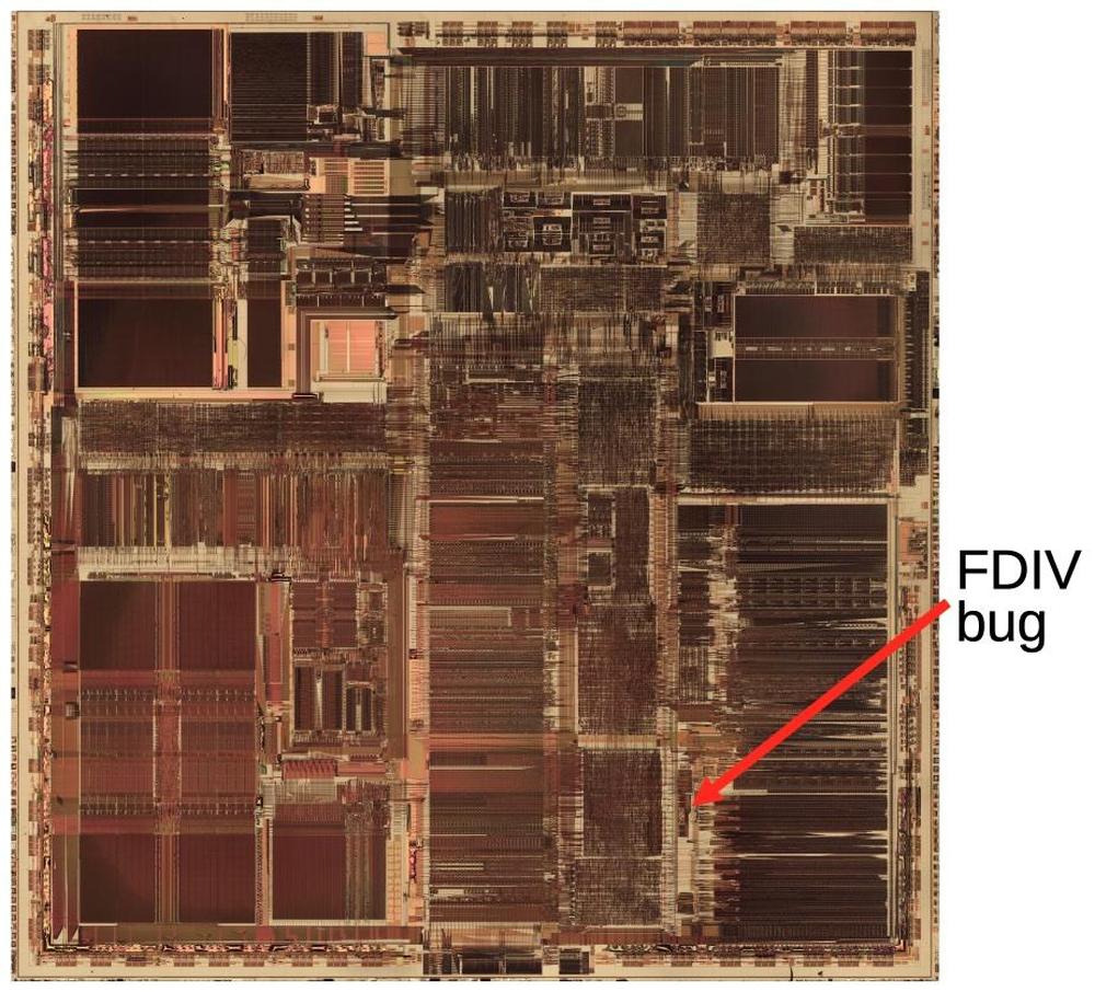
In this article, I discuss the Pentium's division algorithm, show exactly where the bug is on the Pentium chip, take a close look at the circuitry, and explain what went wrong. In brief, the division algorithm uses a lookup table. In 1994, Intel stated that the cause of the bug was that five entries were omitted from the table due to an error in a script. However, my analysis shows that 16 entries were omitted due to a mathematical mistake in the definition of the lookup table. Five of the missing entries trigger the bug— also called the FDIV bug after the floating-point division instruction "FDIV"—while 11 of the missing entries have no effect.

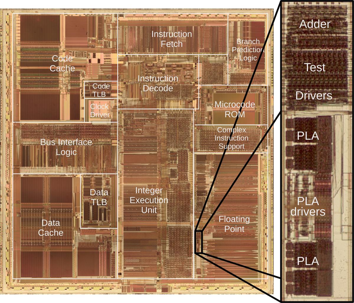
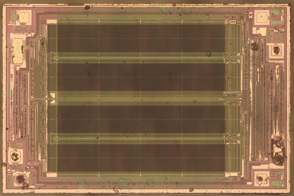
This die photo of the Pentium shows the location of the FDIV bug. Click this image (or any other) for a larger version.

This die photo of the Pentium shows the location of the FDIV bug. Click this image (or any other) for a larger version.

Although Professor Nicely brought attention to the FDIV bug, he wasn't the first to find it. In May 1994, Intel's internal testing of the Pentium revealed that very rarely, floating-point division was slightly inaccurate.1 Since only one in 9 billion values caused the problem, Intel's view was that the problem was trivial: "This doesn't even qualify as an errata." Nonetheless, Intel quietly revised the Pentium circuitry to fix the problem.

A few months later, in October, Nicely noticed erroneous results in his prime number computations.2 He soon determined that 1/824633702441 was wrong on three different Pentium computers, but his older computers gave the right answer. He called Intel tech support but was brushed off, so Nicely emailed a dozen computer magazines and individuals about the bug. One of the recipients was Andrew Schulman, author of "Undocumented DOS". He forwarded the email to Richard Smith, cofounder of a DOS software tools company. Smith posted the email on a Compuserve forum, a 1990s version of social media.

A reporter for the journal Electronic Engineering Times spotted the Compuserve post and wrote about the Pentium bug in the November 7 issue: Intel fixes a Pentium FPU glitch. In the article, Intel explained that the bug was in a component of the chip called a PLA (Programmable Logic Array) that acted as a lookup table for the division operation. Intel had fixed the bug in the latest Pentiums and would replace faulty processors for concerned customers.3

The problem might have quietly ended here, except that Intel decided to restrict which customers could get a replacement. If a customer couldn't convince an Intel engineer that they needed the accuracy, they couldn't get a fixed Pentium. Users were irate to be stuck with faulty chips so they took their complaints to online groups such as comp.sys.intel. The controversy spilled over into the offline world on November 22 when CNN reported on the bug. Public awareness of the Pentium bug took off as newspapers wrote about the bug and Intel became a punchline on talk shows.4

The situation became intolerable for Intel on December 12 when IBM announced that it was stopping shipments of Pentium computers.5 On December 19, less than two months after Nicely first reported the bug, Intel gave in and announced that it would replace the flawed chips for all customers.6 This recall cost Intel $475 million (over a billion dollars in current dollars).

Meanwhile, engineers and mathematicians were analyzing the bug, including Tim Coe, an engineer who had designed floating-point units.7 Remarkably, by studying the Pentium's bad divisions, Coe reverse-engineered the Pentium's division algorithm and determined why it went wrong. Coe and others wrote papers describing the mathematics behind the Pentium bug.8 But until now, nobody has shown how the bug is implemented in the physical chip itself.

A quick explanation of floating point numbers

At this point, I'll review a few important things about floating point numbers. A binary number can have a fractional part, similar to a decimal number. For instance, the binary number 11.1001 has four digits after the binary point. (The binary point "." is similar to the decimal point, but for a binary number.) The first digit after the binary point represents 1/2, the second represents 1/4, and so forth. Thus, 11.1001 corresponds to 3 + 1/2 + 1/16 = 3.5625. A "fixed point" number such as this can express a fractional value, but its range is limited.

Floating point numbers, on the other hand, include very large numbers such as 6.02×10²³ and very small numbers such as 1.055×10⁻³⁴. In decimal, 6.02×10²³ has a significand (or mantissa) of 6.02, multiplied by a power of 10 with an exponent of 23. In binary, a floating point number is represented similarly, with a significand and exponent, except the significand is multiplied by a power of 2 rather than 10.

Computers have used floating point since the early days of computing, especially for scientific computing. For many years, different computers used incompatible formats for floating point numbers. Eventually, a standard arose when Intel developed the 8087 floating point coprocessor chip for use with the 8086/8088 processor. The characteristics of this chip became a standard (IEEE 754) in 1985.9 Subsequently, most computers, including the Pentium, implemented floating point numbers according to this standard. The result of a basic arithmetic operation is supposed to be accurate up to the last bit of the significand. Unfortunately, division on the Pentium was occasionally much, much worse.

How SRT division works

How does a computer perform division? The straightforward way is similar to grade-school long division, except in binary. That approach was used in the Intel 486 and earlier processors, but the process is slow, taking one clock cycle for each bit of the quotient. The Pentium uses a different approach called SRT,10 performing division in base four. Thus, SRT generates two bits of the quotient per step, rather than one, so division is twice as fast. I'll explain SRT in a hand-waving manner with a base-10 example; rigorous explanations are available elsewhere.

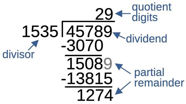
The diagram below shows base-10 long division, with the important parts named. The dividend is divided by the divisor, yielding the quotient. In each step of the long division algorithm, you generate one more digit of the quotient. Then you multiply the divisor (1535) by the quotient digit (2) and subtract this from the dividend, leaving a partial remainder. You multiply the partial remainder by 10 and then repeat the process, generating a quotient digit and partial remainder at each step. The diagram below stops after two quotient digits, but you can keep going to get as much accuracy as desired.

Base-10 division, naming the important parts.

Base-10 division, naming the important parts.

Note that division is more difficult than multiplication since there is no easy way to determine each quotient digit. You have to estimate a quotient digit, multiply it by the divisor, and then check if the quotient digit is correct. For example, you have to check carefully to see if 1535 goes into 4578 two times or three times.

The SRT algorithm makes it easier to select the quotient digit through an unusual approach: it allows negative digits in the quotient. With this change, the quotient digit does not need to be exact. If you pick a quotient digit that is a bit too large, you can use a negative number for the next digit: this will counteract the too-large digit since the next divisor will be added rather than subtracted.

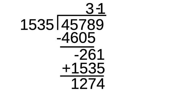
The example below shows how this works. Suppose you picked 3 instead of 2 as the first quotient digit. Since 3 is too big, the partial remainder is negative (-261). In normal division, you'd need to try again with a different quotient digit. But with SRT, you keep going, using a negative digit (-1) for the quotient digit in the next step. At the end, the quotient with positive and negative digits can be converted to the standard form: 3×10-1 = 29, the same quotient as before.

Base-10 division, using a negative quotient digit. The result is the same as the previous example.

Base-10 division, using a negative quotient digit. The result is the same as the previous example.

One nice thing about the SRT algorithm is that since the quotient digit only needs to be close, a lookup table can be used to select the quotient digit. Specifically, the partial remainder and divisor can be truncated to a few digits, making the lookup table a practical size. In this example, you could truncate 1535 and 4578 to 15 and 45, the table says that 15 goes into 45 three times, and you can use 3 as your quotient digit.

Instead of base 10, the Pentium uses the SRT algorithm in base 4: groups of two bits. As a result, division on the Pentium is twice as fast as standard binary division. With base-4 SRT, each quotient digit can be -2, -1, 0, 1, or 2. Multiplying by any of these values is very easy in hardware since multiplying by 2 can be done by a bit shift. Base-4 SRT does not require quotient digits of -3 or 3; this is convenient since multiplying by 3 is somewhat difficult. To summarize, base-4 SRT is twice as fast as regular binary division, but it requires more hardware: a lookup table, circuitry to add or subtract multiples of 1 or 2, and circuitry to convert the quotient to the standard form.

Structure of the Pentium's lookup table

The purpose of the SRT lookup table is to provide the quotient digit. That is, the table takes the partial remainder p and the divisor d as inputs and provides an appropriate quotient digit. The Pentium's lookup table is the cause of the division bug, as was explained in 1994. The table was missing five entries; if the SRT algorithm accesses one of these missing entries, it generates an incorrect result. In this section, I'll discuss the structure of the lookup table and explain what went wrong.

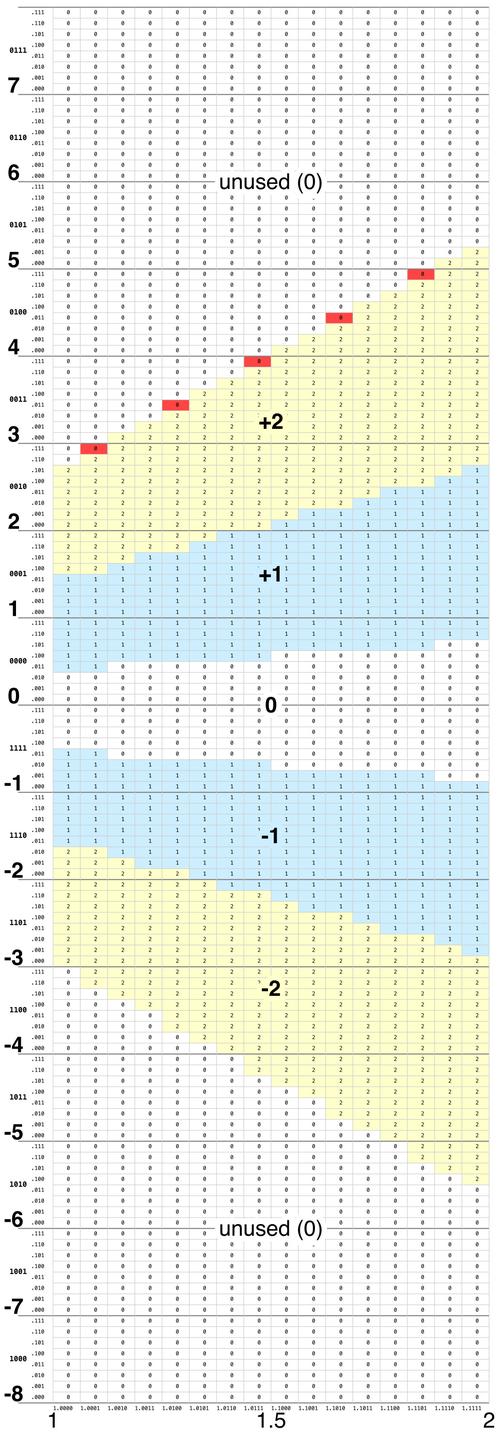
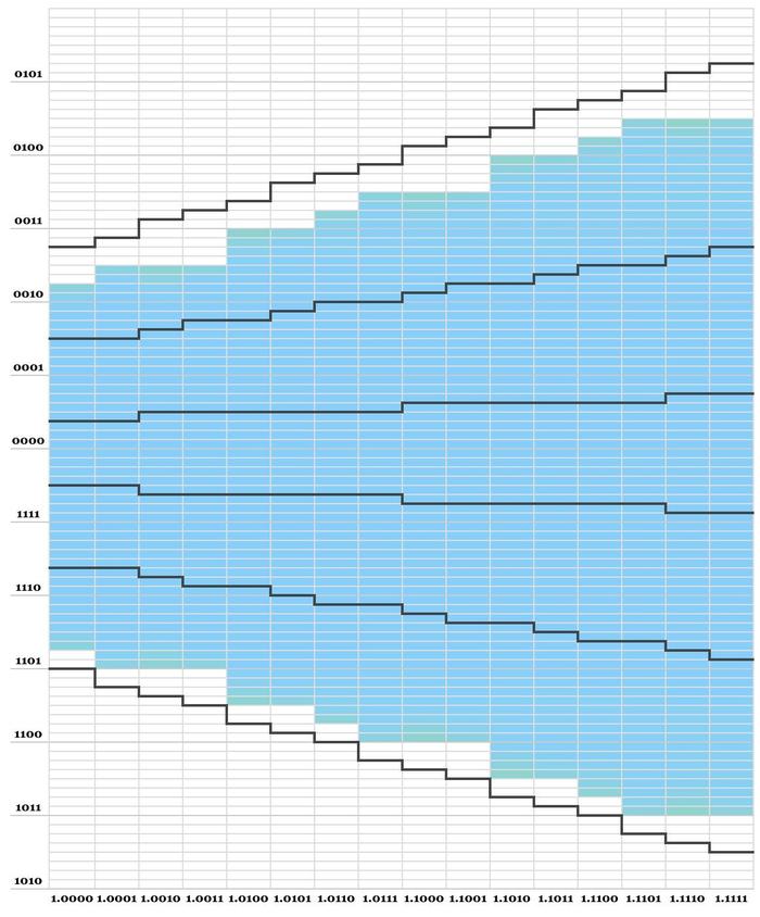
The Pentium's lookup table contains 2048 entries, as shown below. The table has five regions corresponding to the quotient digits +2, +1, 0, -1, and -2. Moreover, the upper and lower regions of the table are unused (due to the mathematics of SRT). The unused entries were filled with 0, which turns out to be very important. In particular, the five red entries need to contain +2 but were erroneously filled with 0.

The 2048-entry lookup table used in the Pentium for division. The divisor is along the X-axis, from 1 to 2. The partial remainder is along the Y-axis, from -8 to 8. Click for a larger version.

The 2048-entry lookup table used in the Pentium for division. The divisor is along the X-axis, from 1 to 2. The partial remainder is along the Y-axis, from -8 to 8. Click for a larger version.

When the SRT algorithm uses the table, the partial remainder p and the divisor d are inputs. The divisor (scaled to fall between 1 and 2) provides the X coordinate into the table, while the partial remainder (between -8 and 8) provides the Y coordinate. The details of the table coordinates will be important, so I'll go into some detail. To select a cell, the divisor (X-axis) is truncated to a 5-bit binary value 1.dddd. (Since the first digit of the divisor is always 1, it is ignored for the table lookup.) The partial remainder (Y-axis) is truncated to a 7-bit signed binary value pppp.ppp. The 11 bits indexing into the table result in a table with 211 (2048) entries. The partial remainder is expressed in 2's complement, so values 0000.000 to 0111.111 are non-negative values from 0 to (almost) 8, while values 1000.000 to 1111.111 are negative values from -8 to (almost) 0. (To see the binary coordinates for the table, click on the image and zoom in.)

The lookup table is implemented in a Programmable Logic Array (PLA)

In this section, I'll explain how the lookup table is implemented in hardware in the Pentium. The lookup table has 2048 entries so it could be stored in a ROM with 2048 two-bit outputs.11 (The sign is not explicitly stored in the table because the quotient digit sign is the same as the partial remainder sign.) However, because the table is highly structured (and largely empty), the table can be stored more compactly in a structure called a Programmable Logic Array (PLA).12 By using a PLA, the Pentium stored the table in just 112 rows rather than 2048 rows, saving an enormous amount of space. Even so, the PLA is large enough on the chip that it is visible to the naked eye, if you squint a bit.

Zooming in on the PLA and associated circuitry on the Pentium die.

Zooming in on the PLA and associated circuitry on the Pentium die.

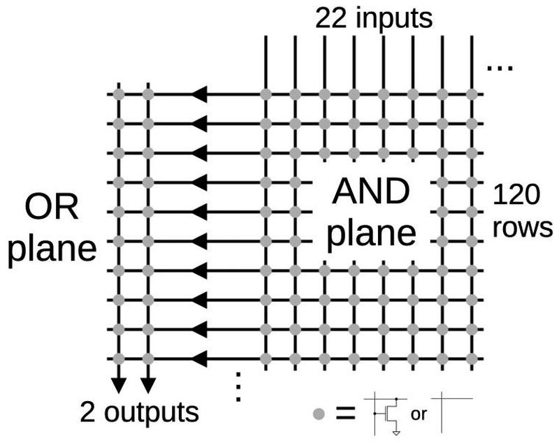
The idea of a PLA is to provide a dense and flexible way of implementing arbitrary logic functions. Any Boolean logic function can be expressed as a "sum-of-products", a collection of AND terms (products) that are OR'd together (summed). A PLA has a block of circuitry called the AND plane that generates the desired sum terms. The outputs of the AND plane are fed into a second block, the OR plane, which ORs the terms together. The AND plane and the OR plane are organized as grids. Each gridpoint can either have a transistor or not, defining the logic functions. The point is that by putting the appropriate pattern of transistors in the grids, you can create any function. For the division PLA, there are has 22 inputs (the 11 bits from the divisor and partial remainder indices, along with their complements) and two outputs, as shown below.13

A simplified diagram of the division PLA.

A simplified diagram of the division PLA.

A PLA is more compact than a ROM if the structure of the function allows it to be expressed with a small number of terms.14 One difficulty with a PLA is figuring out how to express the function with the minimum number of terms to make the PLA as small as possible. It turns out that this problem is NP-complete in general. Intel used a program called Espresso to generate compact PLAs using heuristics.15

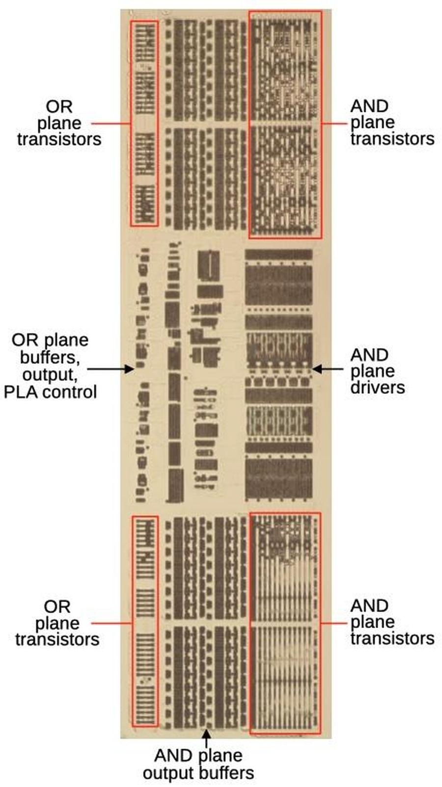
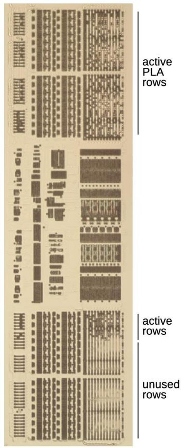
The diagram below shows the division PLA in the Pentium. The PLA has 120 rows, split into two 60-row parts with support circuitry in the middle.16 The 11 table input bits go into the AND plane drivers in the middle, which produce the 22 inputs to the PLA (each table input and its complement). The outputs from the AND plane transistors go through output buffers and are fed into the OR plane. The outputs from the OR plane go through additional buffers and logic in the center, producing two output bits, indicating a ±1 or ±2 quotient. The image below shows the updated PLA that fixes the bug; the faulty PLA looks similar except the transistor pattern is different. In particular, the updated PLA has 46 unused rows at the bottom while the original, faulty PLA has 8 unused rows.

The division PLA with the metal layers removed to show the silicon. This image shows the PLA in the updated Pentium, since that photo came out better.

The division PLA with the metal layers removed to show the silicon. This image shows the PLA in the updated Pentium, since that photo came out better.

The image below shows part of the AND plane of the PLA. At each point in the grid, a transistor can be present or absent. The pattern of transistors in a row determines the logic term for that row. The vertical doped silicon lines (green) are connected to ground. The vertical polysilicon lines (red) are driven with the input bit pattern. If a polysilicon line crosses doped silicon, it forms a transistor (orange) that will pull that row to ground when activated.17 A metal line connects all the transistor rows in a row to produce the output; most of the metal has been removed, but some metal lines are visible at the right.

Part of the AND plane in the fixed Pentium. I colored the first silicon and polysilicon lines green and red respectively.

Part of the AND plane in the fixed Pentium. I colored the first silicon and polysilicon lines green and red respectively.

By carefully examining the PLA under a microscope, I extracted the pattern of transistors in the PLA grid. (This was somewhat tedious.) From the transistor pattern, I could determine the equations for each PLA row, and then generate the contents of the lookup table. Note that the transistors in the PLA don't directly map to the table contents (unlike a ROM). Thus, there is no specific place for transistors corresponding to the 5 missing table entries.

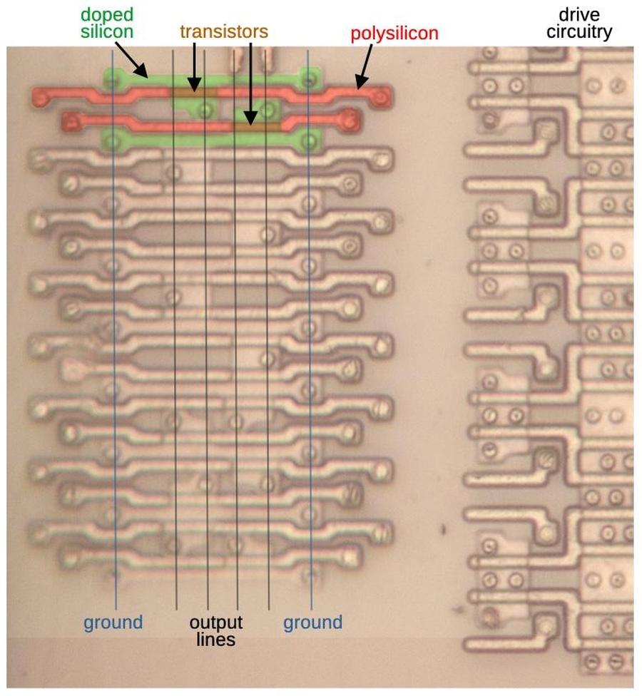
The left-hand side of the PLA implements the OR planes (below). The OR plane determines if the row output produces a quotient of 1 or 2. The OR plane is oriented 90° relative to the AND plane: the inputs are horizontal polysilicon lines (red) while the output lines are vertical. As before, a transistor (orange) is formed where polysilicon crosses doped silicon. Curiously, each OR plane has four outputs, even though the PLA itself has two outputs.18

Part of the OR plane of the division PLA. I removed the metal layers to show the underlying silicon and polysilicon. I drew lines for ground and outputs, showing where the metal lines were.

Part of the OR plane of the division PLA. I removed the metal layers to show the underlying silicon and polysilicon. I drew lines for ground and outputs, showing where the metal lines were.

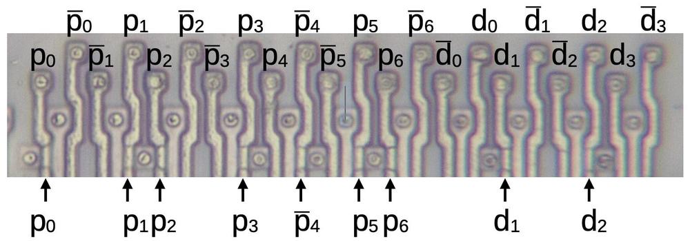
Next, I'll show exactly how the AND plane produces a term. For the division table, the inputs are the 7 partial remainder bits and 4 divisor bits, as explained earlier. I'll call the partial remainder bits p6p5p4p3.p2p1p0 and the divisor bits 1.d3d2d1d0. These 11 bits and their complements are fed vertically into the PLA as shown at the top of the diagram below. These lines are polysilicon, so they will form transistor gates, turning on the corresponding transistor when activated. The arrows at the bottom point to nine transistors in the first row. (It's tricky to tell if the polysilicon line passes next to doped silicon or over the silicon, so the transistors aren't always obvious.) Looking at the transistors and their inputs shows that the first term in the PLA is generated by p0p1p2p3p4'p5p6d1d2.

The first row of the division PLA in a faulty Pentium.

The first row of the division PLA in a faulty Pentium.

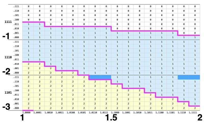
The diagram below is a closeup of the lookup table, showing how this PLA row assigns the value 1 to four table cells (dark blue). You can think of each term of the PLA as pattern-matching to a binary pattern that can include "don't care" values. The first PLA term (above) matches the pattern P=110.1111, D=x11x, where the "don't care" x values can be either 0 or 1. Since one PLA row can implement multiple table cells, the PLA is more efficient than a ROM; the PLA uses 112 rows, while a ROM would require 2048 rows.

The first entry in the PLA assigns the value 1 to the four dark blue cells.

The first entry in the PLA assigns the value 1 to the four dark blue cells.

Geometrically, you can think of each PLA term (row) as covering a rectangle or rectangles in the table. However, the rectangle can't be arbitrary, but must be aligned on a bit boundary. Note that each "bump" in the table boundary (magenta) requires a separate rectangle and thus a separate PLA row. (This will be important later.)

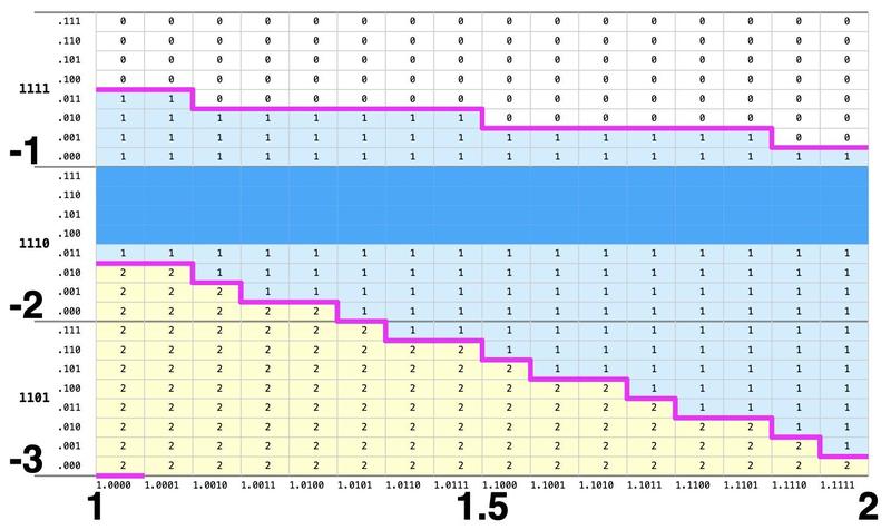
One PLA row can generate a large rectangle, filling in many table cells at once, if the region happens to be aligned nicely. For instance, the third term in the PLA matches d=xxxx, p=11101xx. This single PLA row efficiently fills in 64 table cells as shown below, replacing the 64 rows that would be required in a ROM.

The third entry in the PLA assigns the value 1 to the 64 dark blue cells.

The third entry in the PLA assigns the value 1 to the 64 dark blue cells.

To summarize, the pattern of transistors in the PLA implements a set of equations, which define the contents of the table, setting the quotient to 1 or 2 as appropriate. Although the table has 2048 entries, the PLA represents the contents in just 112 rows. By carefully examining the transistor pattern, I determined the table contents in a faulty Pentium and a fixed Pentium.

The mathematical bounds of the lookup table

As shown earlier, the lookup table has regions corresponding to quotient digits of +2, +1, 0, -1, and -2. These regions have irregular, slanted shapes, defined by mathematical bounds. In this section, I'll explain these mathematical bounds since they are critical to understanding how the Pentium bug occurred.

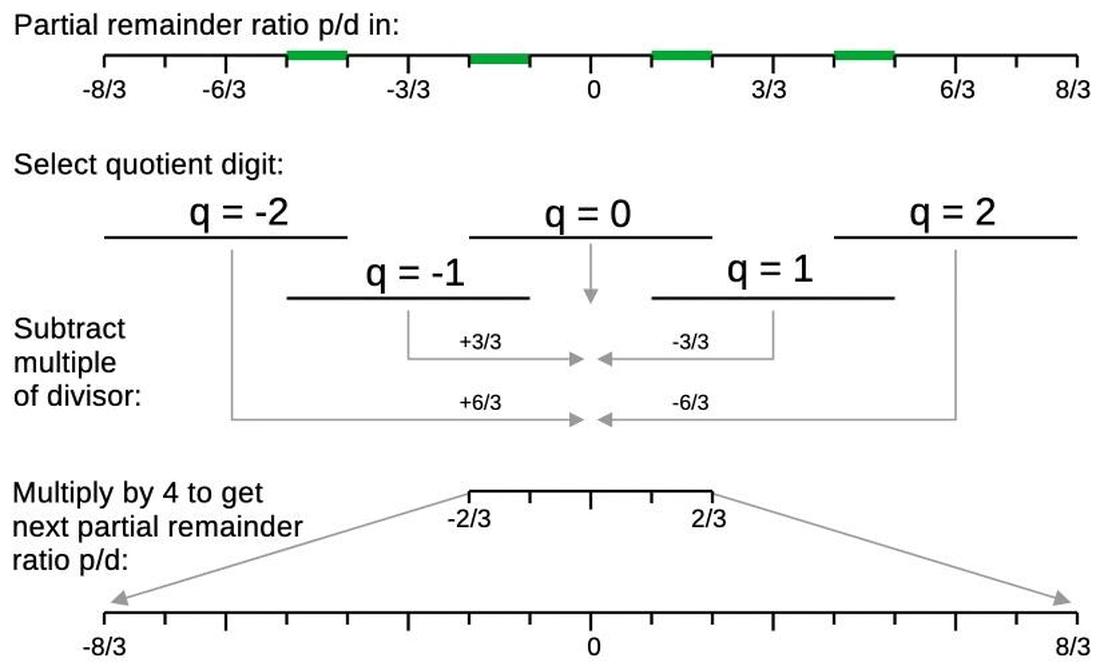
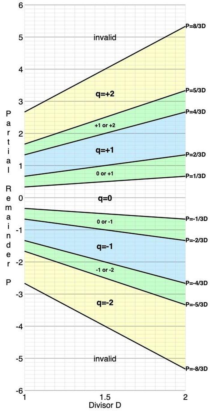
The essential step of the division algorithm is to divide the partial remainder p by the divisor d to get the quotient digit. The following diagram shows how p/d determines the quotient digit. The ratio p/d will define a point on the line at the top. (The point will be in the range [-8/3, 8/3] for mathematical reasons.) The point will fall into one of the five lines below, defining the quotient digit q. However, the five quotient regions overlap; if p/d is in one of the green segments, there are two possible quotient digits. The next part of the diagram illustrates how subtracting q*d from the partial remainder p shifts p/d into the middle, between -2/3 and 2/3. Finally, the result is multiplied by 4 (shifted left by two bits), expanding19 the interval back to [-8/3, 8/3], which is the same size as the original interval. The 8/3 bound may seem arbitrary, but the motivation is that it ensures that the new interval is the same size as the original interval, so the process can be repeated. (The bounds are all thirds for algebraic reasons; the value 3 comes from base 4 minus 1.20)

The input to a division step is processed, yielding the input to the next step.

The input to a division step is processed, yielding the input to the next step.

Note that the SRT algorithm has some redundancy, but cannot handle q values that are "too wrong". Specifically, if p/d is in a green region, then either of two q values can be selected. However, the algorithm cannot recover from a bad q value in general. The relevant case is that if q is supposed to be 2 but 0 is selected, the next partial remainder will be outside the interval and the algorithm can't recover. This is what causes the FDIV bug.

The diagram below shows the structure of the SRT lookup table (also called the P-D table since the axes are p and d). Each bound in the diagram above turns into a line in the table. For instance, the green segment above with p/d between 4/3 and 5/3 turns into a green region in the table below with 4/3 d ≤ p ≤ 5/3 d. These slanted lines show the regions in which a particular quotient digit q can be used.

The P-D table specifies the quotient digit for a partial remainder (Y-axis) and divisor (X-axis).

The P-D table specifies the quotient digit for a partial remainder (Y-axis) and divisor (X-axis).

The lookup table in the Pentium is based on the above table, quantized with a q value in each cell. However, there is one more constraint to discuss.

Carry-save and carry-lookahead adders

The Pentium's division circuitry uses a special circuit to perform addition and subtraction efficiently: the carry-save adder. One consequence of this adder is that each access to the lookup table may go to the cell just below the "right" cell. This is expected and should be fine, but in very rare and complicated circumstances, this behavior causes an access to one of the Pentium's five missing cells, triggering the division bug. In this section, I'll discuss why the division circuitry uses a carry-save adder, how the carry-save adder works, and how the carry-save adder triggers the FDIV bug.

The problem with addition is that carries make addition slow. Consider calculating 99999+1 by hand. You'll start with 9+1=10, then carry the one, generating another carry, which generates another carry, and so forth, until you go through all the digits. Computer addition has the same problem. If you're adding, say, two 64-bit numbers, the low-order bits can generate a carry that then propagates through all 64 bits. The time for the carry signal to go through 64 layers of circuitry is significant and can limit CPU performance. As a result, CPUs use special circuits to make addition faster.

The Pentium's division circuitry uses an unusual adder circuit called a carry-save adder to add (or subtract) the divisor and the partial remainder. A carry-save adder speeds up addition if you are performing a bunch of additions, as happens during division. The idea is that instead of adding a carry to each digit as it happens, you hold onto the carries in a separate word. As a decimal example, 499+222 would be 611 with carries 011; you don't carry the one to the second digit, but hold onto it. The next time you do an addition, you add in the carries you saved previously, and again save any new carries. The advantage of the carry-save adder is that the sum and carry at each digit position can be computed in parallel, which is fast. The disadvantage is that you need to do a slow addition at the end of the sequence of additions to add in the remaining carries to get the final answer. But if you're performing multiple additions (as for division), the carry-save adder is faster overall.

The carry-save adder creates a problem for the lookup table. We need to use the partial remainder as an index into the lookup table. But the carry-save adder splits the partial remainder into two parts: the sum bits and the carry bits. To get the table index, we need to add the sum bits and carry bits together. Since this addition needs to happen for every step of the division, it seems like we're back to using a slow adder and the carry-save adder has just made things worse.

The trick is that we only need 7 bits of the partial remainder for the table index, so we can use a different type of adder—a carry-lookahead adder—that calculates each carry in parallel using brute force logic. The logic in a carry-lookahead adder gets more and more complex for each bit so a carry-lookahead adder is impractical for large words, but it is practical for a 7-bit value.

The photo below shows the carry-lookahead adder used by the divider. Curiously, the adder is an 8-bit adder but only 7 bits are used; perhaps the 8-bit adder was a standard logic block at Intel.21 I'll just give a quick summary of the adder here, and leave the details for another post. At the top, logic gates compute signals in parallel for each of the 8 pairs of inputs: sum, carry generate, and carry propagate. Next, the complex carry-lookahead logic determines in parallel if there will be a carry at each position. Finally, XOR gates apply the carry to each bit. The circuitry in the middle is used for testing; see the footnote.22 At the bottom, the drivers amplify control signals for various parts of the adder and send the PLA output to other parts of the chip.23 By counting the blocks of repeated circuitry, you can see which blocks are 8 bits wide, 11, bits wide, and so forth. The carry-lookahead logic is different for each bit, so there is no repeated structure.

The carry-lookahead adder that feeds the lookup table. This block of circuitry is just above the PLA on the die. I removed the metal layers, so this photo shows the doped silicon (dark) and the polysilicon (faint gray).

The carry-lookahead adder that feeds the lookup table. This block of circuitry is just above the PLA on the die. I removed the metal layers, so this photo shows the doped silicon (dark) and the polysilicon (faint gray).

The carry-save and carry-lookahead adders may seem like implementation trivia, but they are a critical part of the FDIV bug because they change the constraints on the table. The cause is that the partial remainder is 64 bits,24 but the adder that computes the table index is 7 bits. Since the rest of the bits are truncated before the sum, the partial remainder sum for the table index can be slightly lower than the real partial remainder. Specifically, the table index can be one cell lower than the correct cell, an offset of 1/8. Recall the earlier diagram with diagonal lines separating the regions. Some (but not all) of these lines must be shifted down by 1/8 to account for the carry-save effect, but Intel made the wrong adjustment, which is the root cause of the FDIV error. (This effect was well-known at the time and mentioned in papers on SRT division, so Intel shouldn't have gotten it wrong.)

An interesting thing about the FDIV bug is how extremely rare it is. With 5 bad table entries out of 2048, you'd expect erroneous divides to be very common. However, for complicated mathematical reasons involving the carry-save adder the missing table entries are almost never encountered: only about 1 in 9 billion random divisions will encounter a problem. To hit a missing table entry, you need an "unlucky" result from the carry-save adder multiple times in a row, making the odds similar to winning the lottery, if the lottery prize were a division error.25

What went wrong in the lookup table

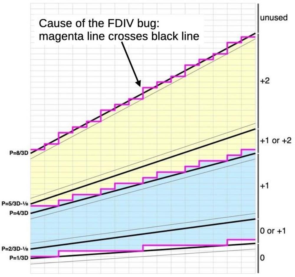
I consider the diagram below to be the "smoking gun" that explains how the FDIV bug happens: the top magenta line should be above the sloping black line, but it crosses the black line repeatedly. The magenta line carefully stays above the gray line, but that's the wrong line. In other words, Intel picked the wrong bounds line when defining the +2 region of the table. In this section, I'll explain why that causes the bug.

The top half of the lookup table, explaining the root of the FDIV bug.

The top half of the lookup table, explaining the root of the FDIV bug.

The diagram is colored according to the quotient values stored in the Pentium's lookup table: yellow is +2, blue is +1, and white is 0, with magenta lines showing the boundaries between different values. The diagonal black lines are the mathematical constraints on the table, defining the region that must be +2, the region that can be +1 or +2, the region that must be +1, and so forth. For the table to be correct, each cell value in the table must satisfy these constraints. The middle magenta line is valid: it remains between the two black lines (the redundant +1 or +2 region), so all the cells that need to be +1 are +1 and all the cells that need to be +2 are +2, as required. Likewise, the bottom magenta line remains between the black lines. However, the top magenta line is faulty: it must remain above the top black line, but it crosses the black line. The consequence is that some cells that need to be +2 end up holding 0: these are the missing cells that caused the FDIV bug.

Note that the top magenta line stays above the diagonal gray line while following it as closely as possible. If the gray line were the correct line, the table would be perfect. Unfortunately, Intel picked the wrong constraint line for the table's upper bound when the table was generated.26

But why are some diagonal lines lowered by 1/8 and other lines are not lowered? As explained in the previous section, as a consequence of the carry-save adder truncation, the table lookup may end up one cell lower than the actual p value would indicate, i.e. the p value for the table index is 1/8 lower than that actual value. Thus, both the correct cell and the cell below must satisfy the SRT constraints. Thus, the line moves down if that makes the constraints stricter but does not move down if that would expand the redundant area. In particular, the top line must not be move down, but clearly Intel moved the line down and generated the faulty lookup table.

Intel, however, has a different explanation for the bug. The Intel white paper states that the problem was in a script that downloaded the table into a PLA: an error caused the script to omit a few entries from the PLA.27 I don't believe this explanation: the missing terms match a mathematical error, not a copying error. I suspect that Intel's statement is technically true but misleading: they ran a C program (which they called a script) to generate the table but the program had a mathematical error in the bounds.

In his book "The Pentium Chronicles", Robert Colwell, architect of the Pentium Pro, provides a different explanation of the FDIV bug. Colwell claims that the Pentium design originally used the same lookup table as the 486, but shortly before release, the engineers were pressured by management to shrink the circuitry to save die space. The engineers optimized the table to make it smaller and had a proof that the optimization would work. Unfortunately, the proof was faulty, but the testers trusted the engineers and didn't test the modification thoroughly, causing the Pentium to be released with the bug. The problem with this explanation is that the Pentium was designed from the start with a completely different division algorithm from the 486: the Pentium uses radix-4 SRT, while the 486 uses standard binary division. Since the 486 doesn't have a lookup table, the story falls apart. Moreover, the PLA could trivially have been made smaller by removing the 8 unused rows, so the engineers clearly weren't trying to shrink it. My suspicion is that since Colwell developed the Pentium Pro in Oregon but the original Pentium was developed in California, Colwell didn't get firsthand information on the Pentium problems.

How Intel fixed the bug

Intel's fix for the bug was straightforward but also surprising. You'd expect that Intel added the five missing table values to the PLA, and this is what was reported at the time. The New York Times wrote that Intel fixed the flaw by adding several dozen transistors to the chip. EE Times wrote that "The fix entailed adding terms, or additional gate-sequences, to the PLA."

However, the updated PLA (below) shows something entirely different. The updated PLA is exactly the same size as the original PLA. However, about 1/3 of the terms were removed from the PLA, eliminating hundreds of transistors. Only 74 of the PLA's 120 rows are used, and the rest are left empty. (The original PLA had 8 empty rows.) How could removing terms from the PLA fix the problem?

The updated PLA has 46 unused rows.

The updated PLA has 46 unused rows.

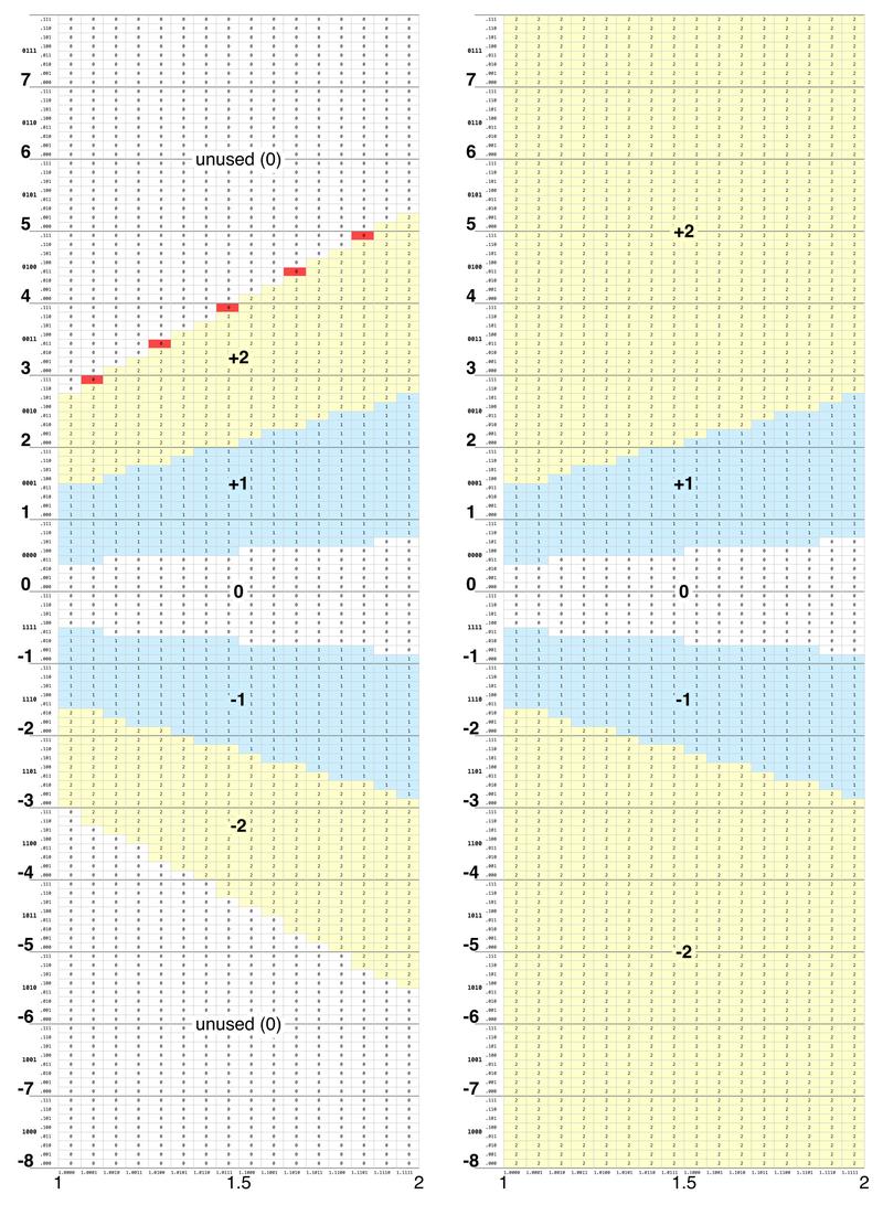
The explanation is that Intel didn't just fill in the five missing table entries with the correct value of 2. Instead, Intel filled all the unused table entries with 2, as shown below. This has two effects. First, it eliminates any possibility of hitting a mistakenly-empty entry. Second, it makes the PLA equations much simpler. You might think that more entries in the table would make the PLA larger, but the number of PLA terms depends on the structure of the data. By filling the unused cells with 2, the jagged borders between the unused regions (white) and the "2" regions (yellow) disappear. As explained earlier, a large rectangle can be covered by a single PLA term, but a jagged border requires a lot of terms. Thus, the updated PLA is about 1/3 smaller than the original, flawed PLA. One consequence is that the terms in the new PLA are completely different from the terms in the old PLA so one can't point to the specific transistors that fixed the bug.

Comparison of the faulty lookup table (left) and the corrected lookup table (right).

Comparison of the faulty lookup table (left) and the corrected lookup table (right).

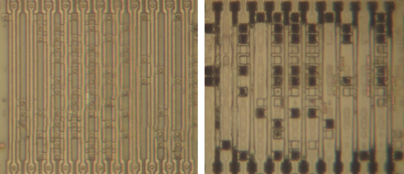
The image below shows the first 14 rows of the faulty PLA and the first 14 rows of the fixed PLA. As you can see, the transistor pattern (and thus the PLA terms) are entirely different. The doped silicon is darkened in the second image due to differences in how I processed the dies to remove the metal layers.

Top of the faulty PLA (left) and the fixed PLA (right). The metal layers were removed to show the silicon of the transistors. (Click for a larger image.)

Top of the faulty PLA (left) and the fixed PLA (right). The metal layers were removed to show the silicon of the transistors. (Click for a larger image.)

Impact of the FDIV bug

How important is the Pentium bug? This became a highly controversial topic. A failure of a random division operation is very rare: about one in 9 billion values will trigger the bug. Moreover, an erroneous division is still mostly accurate: the error is usually in the 9th or 10th decimal digit, with rare worst-case error in the 4th significant digit. Intel's whitepaper claimed that a typical user would encounter a problem once every 27,000 years, insignificant compared to other sources of error such as DRAM bit flips. Intel said: "Our overall conclusion is that the flaw in the floating point unit of the Pentium processor is of no concern to the vast majority of users. A few users of applications in the scientific/engineering and financial engineering fields may need to employ either an updated processor without the flaw or a software workaround."

However, IBM performed their own analysis,29 suggesting that the problem could hit customers every few days, and IBM suspended Pentium sales. (Coincidentally, IBM had a competing processor, the PowerPC.) The battle made it to major newspapers; the Los Angeles Times split the difference with Study Finds Both IBM, Intel Off on Error Rate. Intel soon gave in and agreed to replace all the Pentiums, making the issue moot.

I mostly agree with Intel's analysis. It appears that only one person (Professor Nicely) noticed the bug in actual use.28 The IBM analysis seems contrived to hit numbers that trigger the error. Most people would never hit the bug and even if they hit it, a small degradation in floating-point accuracy is unlikely to matter to most people. Looking at society as a whole, replacing the Pentiums was a huge expense for minimal gain. On the other hand, it's reasonable for customers to expect an accurate processor.

Note that the Pentium bug is deterministic: if you use a specific divisor and dividend that trigger the problem, you will get the wrong answer 100% of the time. Pentium engineer Ken Shoemaker suggested that the outcry over the bug was because it was so easy for customers to reproduce. It was hard for Intel to argue that customers would never encounter the bug when customers could trivially see the bug on their own computer, even if the situation was artificial.

Conclusions

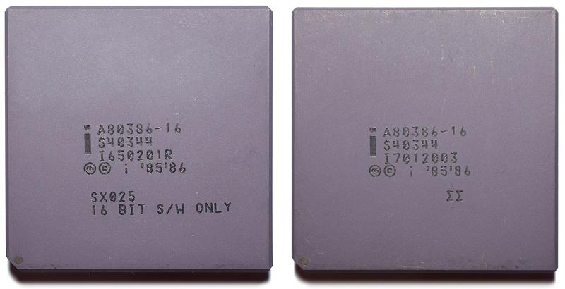
The FDIV bug is one of the most famous processor bugs. By examining the die, it is possible to see exactly where it is on the chip. But Intel has had other important bugs. Some early 386 processors had a 32-bit multiply problem. Unlike the deterministic FDIV bug, the 386 would unpredictably produce the wrong results under particular temperature/voltage/frequency conditions. The underlying issue was a layout problem that didn't provide enough electrical margin to handle the worst-case situation. Intel sold the faulty chips but restricted them to the 16-bit market; bad chips were labeled "16 BIT S/W ONLY", while the good processors were marked with a double sigma. Although Intel had to suffer through embarrassing headlines such as Some 386 Systems Won't Run 32-Bit Software, Intel Says, the bug was soon forgotten.

Bad and good versions of the 386. Note the labels on the bottom line. Photos (L), (R) by Thomas Nguyen, (CC BY-SA 4.0)

Bad and good versions of the 386. Note the labels on the bottom line. Photos (L), (R) by Thomas Nguyen, (CC BY-SA 4.0)

Another memorable Pentium issue was the "F00F bug", a problem where a particular instruction sequence starting with F0 0F would cause the processor to lock up until rebooted.30 The bug was found in 1997 and solved with an operating system update. The bug is presumably in the Pentium's voluminous microcode. The microcode is too complex for me to analyze, so don't expect a detailed blog post on this subject. :-)

You might wonder why Intel needed to release a new revision of the Pentium to fix the FDIV bug, rather than just updating the microcode. The problem was that microcode for the Pentium (and earlier processors) was hard-coded into a ROM and couldn't be modified. Intel added patchable microcode to the Pentium Pro (1995), allowing limited modifications to the microcode. Intel originally implemented this feature for chip debugging and testing. But after the FDIV bug, Intel realized that patchable microcode was valuable for bug fixes too.31 The Pentium Pro stores microcode in ROM, but it also has a static RAM that holds up to 60 microinstructions. During boot, the BIOS can load a microcode patch into this RAM. In modern Intel processors, microcode patches have been used for problems ranging from the Spectre vulnerability to voltage problems.

The Pentium PLA with the top metal layer removed, revealing the M2 and M1 layers. The OR and AND planes are at the top and bottom, with drivers and control logic in the middle.

The Pentium PLA with the top metal layer removed, revealing the M2 and M1 layers. The OR and AND planes are at the top and bottom, with drivers and control logic in the middle.

As the number of transistors in a processor increased exponentially, as described by Moore's Law, processors used more complex circuits and algorithms. Division is one example. Early microprocessors such as the Intel 8080 (1974, 6000 transistors) had no hardware support for division or floating point arithmetic. The Intel 8086 (1978, 29,000 transistors) implemented integer division in microcode but required the 8087 coprocessor chip for floating point. The Intel 486 (1989, 1.2 million transistors) added floating-point support on the chip. The Pentium (1993, 3.1 million transistors) moved to the faster but more complicated SRT division algorithm. The Pentium's division PLA alone has roughly 4900 transistor sites, more than a MOS Technology 6502 processor—one component of the Pentium's division circuitry uses more transistors than an entire 1975 processor.

The long-term effect of the FDIV bug on Intel is a subject of debate. On the one hand, competitors such as AMD benefitted from Intel's error. AMD's ads poked fun at the Pentium's problems by listing features of AMD's chips such as "You don't have to double check your math" and "Can actually handle the rigors of complex calculations like division." On the other hand, Robert Colwell, architect of the Pentium Pro, said that the FDIV bug may have been a net benefit to Intel as it created enormous name recognition for the Pentium, along with a demonstration that Intel was willing to back up its brand name. Industry writers agreed; see The Upside of the Pentium Bug. In any case, Intel survived the FDIV bug; time will tell how Intel survives its current problems.

I plan to write more about the implementation of the Pentium's PLA, the adder, and the test circuitry. Until then, you may enjoy reading about the Pentium Navajo rug. (The rug represents the P54C variant of the Pentium, so it is safe from the FDIV bug.) Thanks to Bob Colwell and Ken Shoemaker for helpful discussions.

Footnotes and references

  1. The book Inside Intel says that Vin Dham, the "Pentium czar", found the FDIV problem in May 1994. The book "The Pentium Chronicles" says that Patrice Roussel, the floating-point architect for Intel's upcoming Pentium Pro processor, found the FDIV problem in Summer 1994. I suspect that the bug was kept quiet inside Intel and was discovered more than once. 

  2. The divisor being a prime number has nothing to do with the bug. It's just a coincidence that the problem was found during research with prime numbers. 

  3. See Nicely's FDIV page for more information on the bug and its history. Other sources are the books Creating the Digital Future, The Pentium Chronicles, and Inside Intel. The New York Times wrote about the bug: Flaw Undermines Accuracy of Pentium Chips. Computerworld wrote Intel Policy Incites User Threats on threats of a class-action lawsuit. IBM's response is described in IBM Deals Blow to a Rival as it Suspends Pentium Sales 

  4. Talk show host David Letterman joked about the Pentium on December 15: "You know what goes great with those defective Pentium chips? Defective Pentium salsa!" Although a list of Letterman-style top ten Pentium slogans circulated, the list was a Usenet creation. There's a claim that Jay Leno also joked about the Pentium, but I haven't found verification. 

  5. Processors have many more bugs than you might expect. Intel's 1995 errata list for the Pentium had "21 errata (including the FDIV problem), 4 changes, 16 clarifications, and 2 documentation changes." See Pentium Processor Specification Update and Intel Releases Pentium Errata List

  6. Intel published full-page newspaper ads apologizing for its handling of the problem, stating: "What Intel continues to believe is an extremely minor technical problem has taken on a life of its own."

    Intel's apology letter, published in Financial Times. Note the UK country code in the phone number.

    Intel's apology letter, published in Financial Times. Note the UK country code in the phone number.


  7. Tim Coe's reverse engineering of the Pentium divider was described on the Usenet group comp.sys.intel, archived here. To summarize, Andreas Kaiser found 23 failing reciprocals. Tim Coe determined that most of these failing reciprocals were of the form 3*(2^(K+30)) - 1149*(2^(K-(2*J))) - delta*(2^(K-(2*J))). He recognized that the factor of 2 indicated a radix-4 divider. The extremely low probability of error indicated the presence of a carry save adder; the odds of both the sum and carry bits getting long patterns of ones were very low. Coe constructed a simulation of the divider that matched the Pentium's behavior and noted which table entries must be faulty. 

  8. The main papers on the FDIV bug are Computational Aspects of the Pentium Affair, It Takes Six Ones to Reach a Flaw, The Mathematics of the Pentium Division Bug, The Truth Behind the Pentium Bug, Anatomy of the Pentium Bug, and Risk Analysis of the Pentium Bug. Intel's whitepaper is Statistical Analysis of Floating Point Flaw in the Pentium Processor; I archived IBM's study here

  9. The Pentium uses floating point numbers that follow the IEEE 754 standard. Internally, floating point numbers are represented with 80 bits: 1 bit for the sign, 15 bits for the exponent, and 64 bits for the significand. Externally, floating point numbers are 32-bit single-precision numbers or 64-bit double-precision numbers. Note that the number of significand bits limits the accuracy of a floating-point number. 

  10. The SRT division algorithm is named after the three people who independently created it in 1957-1958: Sweeney at IBM, Robertson at the University of Illinois, and Tocher at Imperial College London. The SRT algorithm was developed further by Atkins in his PhD research (1970).

    The SRT algorithm became more practical in the 1980s as chips became denser. Taylor implemented the SRT algorithm on a board with 150 chips in 1981. The IEEE floating point standard (1985) led to a market for faster floating point circuitry. For instance, the Weitek 4167 floating-point coprocessor chip (1989) was designed for use with the Intel 486 CPU (datasheet) and described in an influential paper. Another important SRT implementation is the MIPS R3010 (1988), the coprocessor for the R3000 RISC processor. The MIPS R3010 uses radix-4 SRT for division with 9 bits from the partial remainder and 9 bits from the divisor, making for a larger lookup table and adder than the Pentium (link).

    To summarize, when Intel wanted to make division faster on the Pentium (1993), the SRT algorithm was a reasonable choice. Competitors had already implemented SRT and multiple papers explained how SRT worked. The implementation should have been straightforward and bug-free. 

  11. The dimensions of the lookup table can't be selected arbitrarily. In particular, if the table is too small, a cell may need to hold two different q values, which isn't possible. Note that constructing the table is only possible due to the redundancy of SRT. For instance, if some values in the call require q=1 and other values require q=1 or 2, then the value q=1 can be assigned to the cell. 

  12. In the white paper, Intel calls the PLA a Programmable Lookup Array, but that's an error; it's a Programmable Logic Array. 

  13. I'll explain a PLA in a bit more detail in this footnote. An example of a sum-of-products formula with inputs a and b is ab' + a'b + ab. This formula has three sum terms, so it requires three rows in the PLA. However, this formula can be reduced to a + b, which uses a smaller two-row PLA. Note that any formula can be trivially expressed with a separate product term for each 1 output in the truth table. The hard part is optimizing the PLA to use fewer terms. The original PLA patent is probably MOS Transistor Integrated Matrix from 1969. 

  14. A ROM and a PLA have many similarities. You can implement a ROM with a PLA by using the AND terms to decode addresses and the OR terms to hold the data. Alternatively, you can replace a PLA with a ROM by putting the function's truth table into the ROM. ROMs are better if you want to hold arbitrary data that doesn't have much structure (such as the microcode ROMs). PLAs are better if the functions have a lot of underlying structure. The key theoretical difference between a ROM and a PLA is that a ROM activates exactly one row at a time, corresponding to the address, while a PLA may activate one row, no rows, or multiple rows at a time. Another alternative for representing functions is to use logic gates directly (known as random logic); moving from the 286 to the 386, Intel replaced many small PLAs with logic gates, enabled by improvements in the standard-cell software. Intel's design process is described in Coping with the Complexity of Microprocessor Design

  15. In 1982, Intel developed a program called LOGMIN to automate PLA design. The original LOGMIN used an exhaustive exponential search, limiting its usability. See A Logic Minimizer for VLSI PLA Design. For the 386, Intel used Espresso, a heuristic PLA minimizer that originated at IBM and was developed at UC Berkeley. Intel probably used Espresso for the Pentium, but I can't confirm that. 

  16. The Pentium's PLA is split into a top half and a bottom half, so you might expect the top half would generate a quotient of 1 and the bottom half would generate a quotient of 2. However, the rows for the two quotients are shuffled together with no apparent pattern. I suspect that the PLA minimization software generated the order arbitrarily. 

  17. Conceptually, the PLA consists of AND gates feeding into OR gates. To simplify the implementation, both layers of gates are actually NOR gates. Specifically, if any transistor in a row turns on, the row will be pulled to ground, producing a zero. De Morgan's laws show that the two approaches are the same, if you invert the inputs and outputs. I'm ignoring this inversion in the diagrams.

    Note that each square can form a transistor on the left, the right, or both. The image must be examined closely to distinguish these cases. Specifically, if the polysilicon line produces a transistor, horizontal lines are visible in the polysilicon. If there are no horizontal lines, the polysilicon passes by without creating a transistor. 

  18. Each OR plane has four outputs, so there are eight outputs in total. These outputs are combined with logic gates to generate the desired two outputs (quotient of 1 or 2). I'm not sure why the PLA is implemented in this fashion. Each row alternates between an output on the left and an output on the right, but I don't think this makes the layout any denser. As far as I can tell, the extra outputs just waste space. One could imagine combining the outputs in a clever way to reduce the number of terms, but instead the outputs are simply OR'd together. 

  19. The dynamics of the division algorithm are interesting. The computation of a particular division will result in the partial remainder bouncing from table cell to table cell, while remaining in one column of the table. I expect this could be analyzed in terms of chaotic dynamics. Specifically, the partial remainder interval is squished down by the subtraction and then expanded when multiplied by 4. This causes low-order bits to percolate upward so the result is exponentially sensitive to initial conditions. I think that the division behavior satisfies the definition of chaos in Dynamics of Simple Maps, but I haven't investigated this in detail.

    You can see this chaotic behavior with a base-10 division, e.g. compare 1/3.0001 to 1/3.0002:
    1/3.0001=0.33332222259258022387874199947368393726705454969006... 1/3.0002=0.33331111259249383619151572689224512820860216424246...
    Note that the results start off the same but are completely divergent by 15 digits. (The division result itself isn't chaotic, but the sequence of digits is.)

    I tried to make a fractal out of the SRT algorithm and came up with the image below. There are 5 bands for convergence, each made up of 5 sub-bands, each made up of 5 sub-sub bands, and so on, corresponding to the 5 q values.

    A fractal showing convergence or divergence of SRT division as the scale factor (X-axis) ranges from the normal value of 4 to infinity. The Y-axis is the starting partial remainder. The divisor is (arbitrarily) 1.5. Red indicates convergence; gray is darker as the value diverges faster.

    A fractal showing convergence or divergence of SRT division as the scale factor (X-axis) ranges from the normal value of 4 to infinity. The Y-axis is the starting partial remainder. The divisor is (arbitrarily) 1.5. Red indicates convergence; gray is darker as the value diverges faster.


  20. The algebra behind the bound of 8/3 is that p (the partial remainder) needs to be in an interval that stays the same size each step. Each step of division computes pnew = (pold - q*d)*4. Thus, at the boundary, with q=2, you have p = (p-2*d)*4, so 3p=8d and thus p/d = 8/3. Similarly, the other boundary, with q=-2, gives you p/d = -8/3. 

  21. I'm not completely happy with the 8-bit carry-lookahead adder. Coe's mathematical analysis in 1994 showed that the carry-lookahead adder operates on 7 bits. The adder in the Pentium has two 8-bit inputs connected to another part of the division circuit. However, the adder's bottom output bit is not connected to anything. That would suggest that the adder is adding 8 bits and then truncating to 7 bits, which would reduce the truncation error compared to a 7-bit adder. However, when I simulate the division algorithm this way, the FDIV bug doesn't occur. Wiring the bottom input bits to 0 would explain the behavior, but that seems pointless. I haven't examined the circuitry that feeds the adder, so I don't have a conclusive answer. 

  22. Half of the circuitry in the adder block is used to test the lookup table. The reason is that a chip such as the Pentium is very difficult to test: if one out of 3.1 million transistors goes bad, how do you detect it? For a simple processor like the 8080, you can run through the instruction set and be fairly confident that any problem would turn up. But with a complex chip, it is almost impossible to come up with an instruction sequence that would test every bit of the microcode ROM, every bit of the cache, and so forth. Starting with the 386, Intel added circuitry to the processor solely to make testing easier; about 2.7% of the transistors in the 386 were for testing.

    To test a ROM inside the processor, Intel added circuitry to scan the entire ROM and checksum its contents. Specifically, a pseudo-random number generator runs through each address, while another circuit computes a checksum of the ROM output, forming a "signature" word. At the end, if the signature word has the right value, the ROM is almost certainly correct. But if there is even a single bit error, the checksum will be wrong and the chip will be rejected. The pseudo-random numbers and the checksum are both implemented with linear feedback shift registers (LFSR), a shift register along with a few XOR gates to feed the output back to the input. For more information on testing circuitry in the 386, see Design and Test of the 80386, written by Pat Gelsinger, who became Intel's CEO years later. Even with the test circuitry, 48% of the transistor sites in the 386 were untested. The instruction-level test suite to test the remaining circuitry took almost 800,000 clock cycles to run. The overhead of the test circuitry was about 10% more transistors in the blocks that were tested.

    In the Pentium, the circuitry to test the lookup table PLA is just below the 7-bit adder. An 11-bit LFSR creates the 11-bit input value to the lookup table. A 13-bit LFSR hashes the two-bit quotient result from the PLA, forming a 13-bit checksum. The checksum is fed serially to test circuitry elsewhere in the chip, where it is merged with other test data and written to a register. If the register is 0 at the end, all the tests pass. In particular, if the checksum is correct, you can be 99.99% sure that the lookup table is operating as expected. The ironic thing is that this test circuit was useless for the FDIV bug: it ensured that the lookup table held the intended values, but the intended values were wrong.

    Why did Intel generate test addresses with a pseudo-random sequence instead of a sequential counter? It turns out that a linear feedback shift register (LFSR) is slightly more compact than a counter. This LFSR trick was also used in a touch-tone chip and the program counter of the Texas Instruments TMS 1000 microcontroller (1974). In the TMS 1000, the program counter steps through the program pseudo-randomly rather than sequentially. The program is shuffled appropriately in the ROM to counteract the sequence, so the program executes as expected and a few transistors are saved. 

  23. One unusual feature of the Pentium is that it uses BiCMOS technology: both bipolar and CMOS transistors. Note the distinctive square boxes in the driver circuitry; these are bipolar transistors, part of the high-speed drivers.

    Three bipolar transistors. These transistors transmit the quotient to the rest of
the division circuitry.

    Three bipolar transistors. These transistors transmit the quotient to the rest of the division circuitry.


  24. I think the partial remainder is actually 67 bits because there are three extra bits to handle rounding. Different parts of the floating-point datapath have different widths, depending on what width is needed at that point. 

  25. In this long footnote, I'll attempt to explain why the FDIV bug is so rare, using heatmaps. My analysis of Intel's lookup table shows several curious factors that almost cancel out, making failures rare but not impossible. (For a rigorous explanation, see It Takes Six Ones to Reach a Flaw and The Mathematics of the Pentium Division Bug. These papers explain that, among other factors, a bad divisor must have six consecutive ones in positions 5 through 10 and the division process must go through nine specific steps, making a bad result extremely uncommon.)

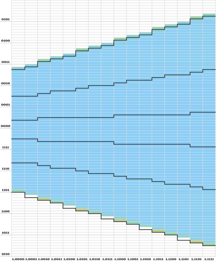
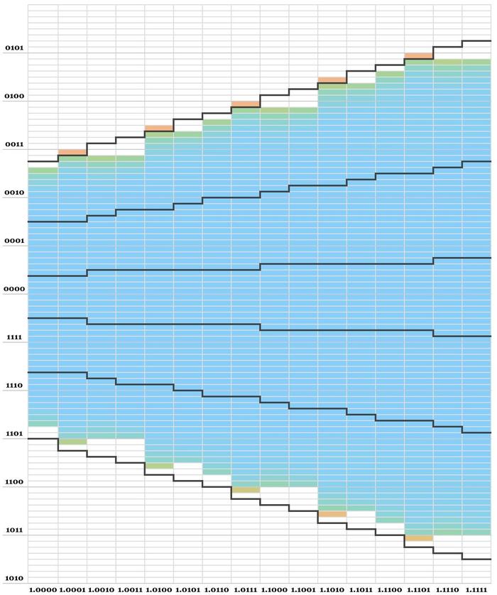
    The diagram below shows a heatmap of how often each table cell is accessed when simulating a generic SRT algorithm with a carry-save adder. The black lines show the boundaries of the quotient regions in the Pentium's lookup table. The key point is that the top colored cell in each column is above the black line, so some table cells are accessed but are not defined in the Pentium. This shows that the Pentium is missing 16 entries, not just the 5 entries that are usually discussed. (For this simulation, I generated the quotient digit directly from the SRT bounds, rather than the lookup table, selecting the digit randomly in the redundant regions.)

    A heatmap showing the table cells accessed by an SRT simulation.

    A heatmap showing the table cells accessed by an SRT simulation.

    The diagram is colored with a logarithmic color scale. The blue cells are accessed approximately uniformly. The green cells at the boundaries are accessed about 2 orders of magnitude less often. The yellow-green cells are accessed about 3 orders of magnitude less often. The point is that it is hard to get to the edge cells since you need to start in the right spot and get the right quotient digit, but it's not extraordinarily hard.

    (The diagram also shows an interesting but ultimately unimportant feature of the Pentium table: at the bottom of the diagram, five white cells are above the back line. This shows that the Pentium assigns values to five table cells that can't be accessed. (This was also mentioned in "The Mathematics of the Pentium Bug".) These cells are in the same columns as the 5 missing cells, so it would be interesting if they were related to the missing cells. But as far as I can tell, the extra cells are due to using a bound of "greater or equals" rather than "greater", unrelated to the missing cells. In any case, the extra cells are harmless.)

    The puzzling factor is that if the Pentium table has 16 missing table cells, and the SRT uses these cells fairly often, you'd expect maybe 1 division out of 1000 or so to be wrong. So why are division errors extremely rare?

    It turns out that the structure of the Pentium lookup table makes some table cells inaccessible. Specifically, the table is arbitrarily biased to pick the higher quotient digit rather than the lower quotient digit in the redundant regions. This has the effect of subtracting more from the partial remainder, pulling the partial remainder away from the table edges. The diagram below shows a simulation using the Pentium's lookup table and no carry-save adder. Notice that many cells inside the black lines are white, indicating that they are never accessed. This is by coincidence, due to arbitrary decisions when constructing in the lookup table. Importantly, the missing cells just above the black line are never accessed, so the missing cells shouldn't cause a bug.

    A heatmap showing the table cells accessed by an SRT simulation using the Pentium's lookup table but no carry-save adder.

    A heatmap showing the table cells accessed by an SRT simulation using the Pentium's lookup table but no carry-save adder.

    Thus, Intel almost got away with the missing table entries. Unfortunately, the carry-save adder makes it possible to reach some of the otherwise inaccessible cells. Because the output from the carry-save adder is truncated, the algorithm can access the table cell below the "right" cell. In the redundant regions, this can yield a different (but still valid) quotient digit, causing the next partial remainder to end up in a different cell than usual. The heatmap below shows the results.

    A heatmap showing the probability of ending up in each table cell when using the Pentium's division algorithm.

    A heatmap showing the probability of ending up in each table cell when using the Pentium's division algorithm.

    In particular, five cells above the black line can be reached: these are instances of the FDIV bug. These cells are orange, indicating that they are about 9 orders of magnitude less likely than the rest of the cells. It's almost impossible to reach these cells, requiring multiple "unlucky" values in a row from the carry-save adder. To summarize, the Pentium lookup table has 16 missing cells. Purely by coincidence, the choices in the lookup table make many cells inaccessible, which almost counteracts the problem. However, the carry-save adder provides a one-in-a-billion path to five of the missing cells, triggering the FDIV bug.

    One irony is that if division errors were more frequent, Intel would have caught the FDIV bug before shipping. But if division errors were substantially less frequent, no customers would have noticed the bug. Inconveniently, the frequency of errors fell into the intermediate zone: errors were too rare for Intel to spot them, but frequent enough for a single user to spot them. (This makes me wonder what other astronomically infrequent errors may be lurking in processors.) 

  26. Anatomy of the Pentium Bug reached a similar conclusion, stating "The [Intel] White Paper attributes the error to a script that incorrectly copied values; one is nevertheless tempted to wonder whether the rule for lowering thresholds was applied to the 8D/3 boundary, which would be an incorrect application because that boundary is serving to bound a threshold from below." (That paper also hypothesizes that the table was compressed to 6 columns, a hypothesis that my examination of the die disproves.) 

  27. The Intel white paper describes the underlying cause of the bug: "After the quantized P-D plot (lookup table) was numerically generated as in Figure 4-1, a script was written to download the entries into a hardware PLA (Programmable Lookup Array). An error was made in this script that resulted in a few lookup entries (belonging to the positive plane of the P-D plot) being omitted from the PLA." The script explanation is repeated in The Truth Behind the Pentium Bug: "An engineer prepared the lookup table on a computer and wrote a script in C to download it into a PLA (programmable logic array) for inclusion in the Pentium's FPU. Unfortunately, due to an error in the script, five of the 1066 table entries were not downloaded. To compound this mistake, nobody checked the PLA to verify the table was copied correctly." My analysis suggests that the table was copied correctly; the problem was that the table was mathematically wrong. 

  28. It's not hard to find claims of people encountering the Pentium division bug, but these seem to be in the "urban legend" category. Either the problem is described second-hand, or the problem is unrelated to division, or the problem happened much too frequently to be the FDIV bug. It has been said that the game Quake would occasionally show the wrong part of a level due to the FDIV bug, but I find that implausible. The "Intel Inside—Don't Divide" Chipwreck describes how the division bug was blamed for everything from database and application server crashes to gibberish text. 

  29. IBM's analysis of the error rate seems contrived, coming up with reasons to use numbers that are likely to cause errors. In particular, IBM focuses on slightly truncated numbers, either numbers with two decimal digits or hardcoded constants. Note that a slightly truncated number is much more likely to hit a problem because its binary representation will have multiple 1's in a row, a necessity to trigger the bug. Another paper Risk Analysis of the Pentium Bug claims a risk of one in every 200 divisions. It depends on "bruised integers", such as 4.999999, which are similarly contrived. I'll also point out that if you start with numbers that are "bruised" or otherwise corrupted, you obviously don't care about floating-point accuracy and shouldn't complain if the Pentium adds slightly more inaccuracy.

    The book "Inside Intel" says that "the IBM analysis was quite wrong" and "IBM's intervention in the Pentium affair was not an example of the company on its finest behavior" (page 364). 

  30. The F00F bug happens when an invalid compare-and-exchange instruction leaves the bus locked. The instruction is supposed to exchange with a memory location, but the invalid instruction specifies a register instead causing unexpected behavior. This is very similar to some undocumented instructions in the 8086 processor where a register is specified when memory is required; see my article Undocumented 8086 instructions, explained by the microcode

  31. For details on the Pentium Pro's patchable microcode, see P6 Microcode Can Be Patched. But patchable microcode dates back much earlier. The IBM System/360 mainframes (1964) had microcode that could be updated in the field, either to fix bugs or to implement new features. These systems stored microcode on metalized Mylar sheets that could be replaced as necessary. In that era, semiconductor ROMs didn't exist, so Mylar sheets were also a cost-effective way to implement read-only storage. See TROS: How IBM mainframes stored microcode in transformers

Antenna diodes in the Pentium processor

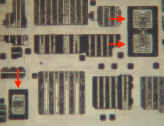
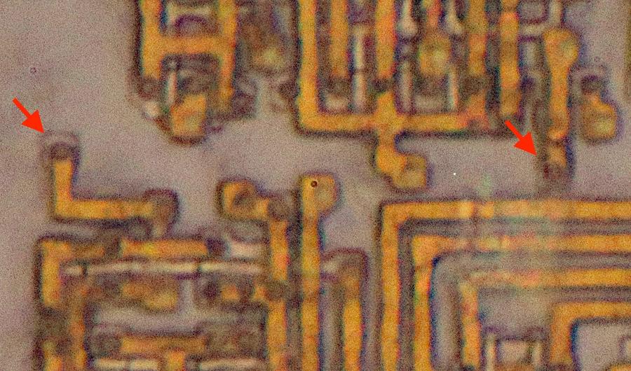
I was studying the silicon die of the Pentium processor and noticed some puzzling structures where signal lines were connected to the silicon substrate for no apparent reason. Two examples are in the photo below, where the metal wiring (orange) connects to small square regions of doped silicon (gray), isolated from the rest of the circuitry. I did some investigation and learned that these structures are "antenna diodes," special diodes that protect the circuitry from damage during manufacturing. In this blog post, I discuss the construction of the Pentium and explain how these antenna diodes work.

Closeup of the Pentium die showing the silicon and bottom metal layer. The arrows indicate connections to two antenna diodes. I removed the top two layers of metal for this photo.

Closeup of the Pentium die showing the silicon and bottom metal layer. The arrows indicate connections to two antenna diodes. I removed the top two layers of metal for this photo.

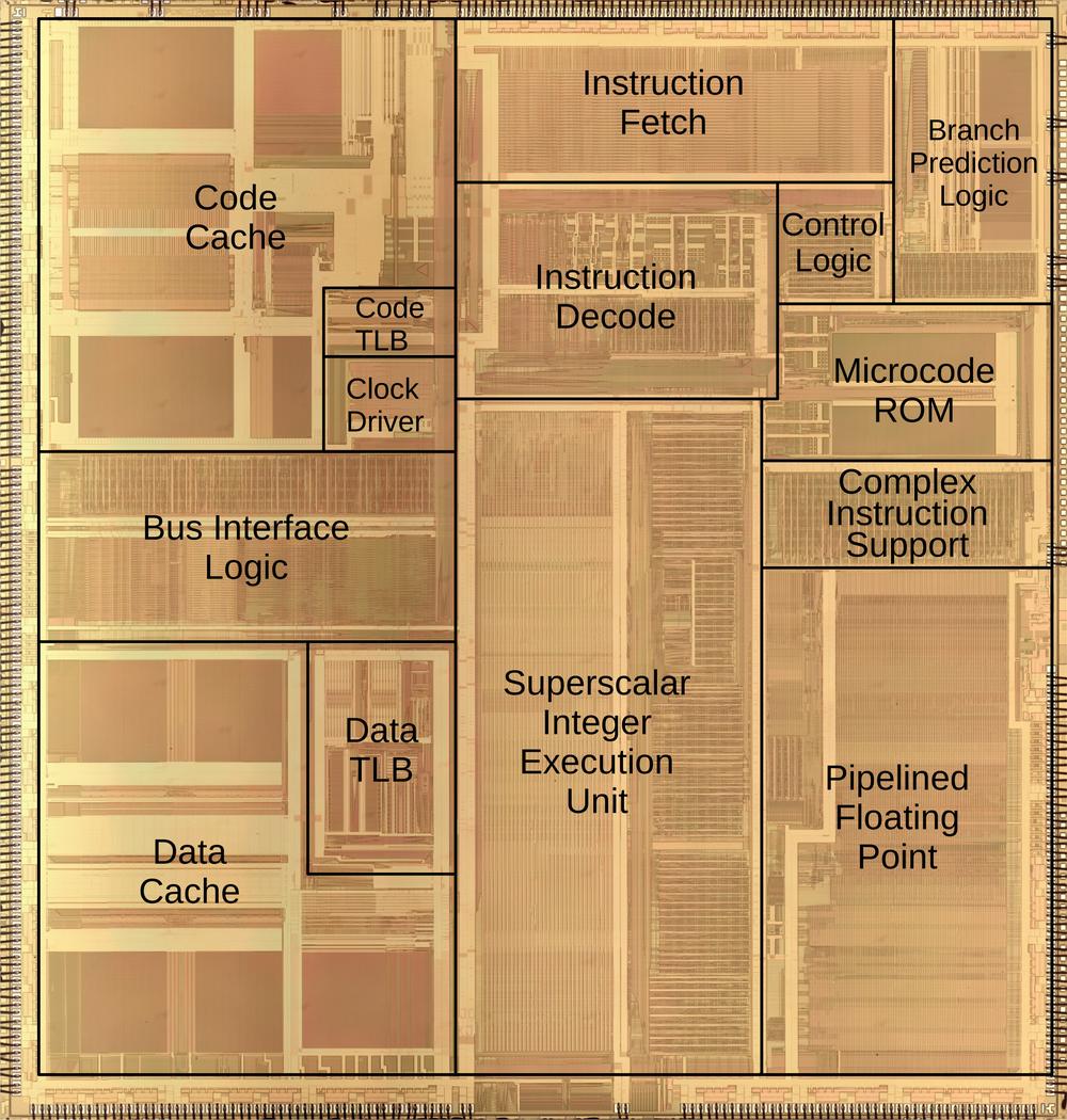
Intel released the Pentium processor in 1993, starting a long-running brand of high-performance processors: the Pentium Pro, Pentium II, and so on. In this post, I'm studying the original Pentium, which has 3.1 million transistors.1 The die photo below shows the Pentium's fingernail-sized silicon die under a microscope. The chip has three layers of metal wiring on top of the silicon so the underlying silicon is almost entirely obscured.

The Pentium die with the main functional blocks labeled. Click this photo (or any other) for a larger version.

The Pentium die with the main functional blocks labeled. Click this photo (or any other) for a larger version.

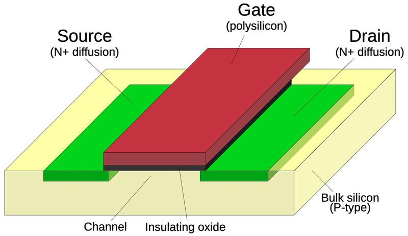
Modern processors are built from CMOS circuitry, which uses two types of transistors: NMOS and PMOS. The diagram below shows how an NMOS transistor is constructed. A transistor can be considered a switch between the source and drain, controlled by the gate. The source and drain regions (green) consist of silicon doped with impurities to change its semiconductor properties, forming N+ silicon. The gate consists of a layer of polysilicon (red), separated from the silicon by an absurdly thin insulating oxide layer. Since the oxide layer is just a few hundred atoms thick,2 it is very fragile and easily damaged by excess voltage. (This is why CMOS chips are sensitive to static electricity.) As we will see, the oxide layer can also be damaged by voltage during manufacturing.

Diagram showing the structure of an NMOS transistor.

Diagram showing the structure of an NMOS transistor.

The Pentium processor is constructed from multiple layers. Starting at the bottom, the Pentium has millions of transistors similar to the diagram above. Polysilicon wiring on top of the silicon not only forms the transistor gates but also provides short-range wiring. Above that, three layers of metal wiring connect the parts of the chip. Roughly speaking, the bottom layer of metal connects to the silicon and polysilicon to construct logic gates from the transistors, while the upper layers of wiring travel longer distances, with one layer for signals traveling horizontally and the other layer for signals traveling vertically. Tiny tungsten plugs called vias provide connections between the different layers of wiring. A key challenge of chip design is routing, directing signals through the multiple layers of wiring while packing the circuitry as densely as possible.

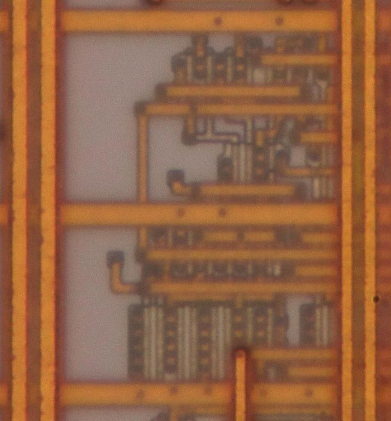
The photo below shows a small region of the Pentium die with the three metal layers visible. The golden vertical lines are the top metal layer, formed from aluminum and copper. Underneath, you can see the horizontal wiring of the middle metal layer. The more complex wiring of the bottom metal layer can be seen, along with the silicon and polysilicon that form transistors. The small black dots are the tungsten vias that connect metal layers, while the larger dark circles are contacts with the underlying silicon or polysilicon. Near the bottom of the photo, the vertical gray bands are polysilicon lines, forming transistor gates. Although the chip appears flat, it has a three-dimensional structure with multiple layers of metal separated by insulating layers of silicon dioxide. This three-dimensional structure will be important in the discussion below. (The metal wiring is much denser over most of the chip; this region is one of the rare spots where all the layers are visible.)

Closeup of the Pentium die showing the metal layers.
The L-shaped hook towards the lower left is a connection to an antenna diode.
This photo shows a tiny part of the floating point unit. To show all the layers in focus, I combined multiple images with focus stacking.

Closeup of the Pentium die showing the metal layers. The L-shaped hook towards the lower left is a connection to an antenna diode. This photo shows a tiny part of the floating point unit. To show all the layers in focus, I combined multiple images with focus stacking.

The manufacturing process for an integrated circuit is extraordinarily complicated but I'll skip over most of the details and focus on how each metal layer is constructed, layer by layer. First, a uniform metal layer is constructed over the silicon wafer. Next, the desired pattern is produced on the surface using a process called photolithography: a light-sensitive chemical called "resist" is applied to the wafer and exposed to light through a patterned mask. The light hardens the resist, creating a protective coating with the pattern of the desired wiring. Finally, the unprotected metal is etched away, leaving the wiring.

In the early days of integrated circuits, the metal was removed with liquid acids, a process called wet etching. Inconveniently, wet etching tended to eat away metal underneath the edges of the mask, which became a problem as integrated circuits became denser and the wires needed to be thinner. The solution was dry etch, using a plasma to remove the metal. By applying a large voltage to plates above and below the chip, a gas such as HCl is ionized into a highly reactive plasma. This plasma attacks the surface (unless it is protected by the resist), removing the unwanted metal. The advantage of dry etching is that it can act vertically (anisotropically), providing more control over the line width.

Although plasma etching improved the etching process, it caused another problem: plasma-induced oxide damage, also called (metaphorically) the "antenna effect."3 The problem is that long metal wires on the chip could pick up an electrical charge from the plasma, producing a large voltage. As described earlier, the thin oxide layer under a transistor's gate is sensitive to voltage damage. The voltage induced by the plasma can destroy the transistor by blowing a hole through the gate oxide or it can degrade the transistor's performance by embedding charges inside the oxide layer.4

Several factors affect the risk of damage from the antenna effect. First, only the transistor's gate is sensitive to the induced voltage, due to the oxide layer. If the wire is also connected to a transistor's source or drain, the wire is "safe" since the source and drain provide connections to the chip's substrate, allowing the charge to dissipate harmlessly. Note that when the chip is completed, every transistor gate is connected to another transistor's source or drain (which provides the signal to the gate), so there is no risk of damage. Thus, the problem can only occur during manufacturing, with a metal line that is connected to a gate on one end but isn't connected on the other end. Moreover, the highest layer of metal is "safe" since everything is connected at that point. Another factor is that the induced voltage is proportional to the length of the metal wire, so short wires don't pose a risk. Finally, only the metal layer currently being etched poses a risk; since the lower layers are insulated by the thick oxide between layers, they won't pick up charge.

These factors motivate several ways to prevent antenna problems.5 First, a long wire can be broken into shorter segments, connected by jumpers on a higher layer. Second, moving long wires to the top metal layer eliminates problems.6 Third, diodes can be added to drain the charge from the wire; these are called "antenna diodes". When the chip is in use, the antenna diodes are reverse-biased so they have no electrical effect. But during manufacturing, the antenna diodes let charge flow to the substrate before it causes problems.

The third solution, the antenna diodes, explains the mysterious connections that I saw in the Pentium. In the diagram below, these diodes are visible on the die as square regions of doped silicon. The larger regions of doped silicon form PMOS transistors (upper) and NMOS transistors (lower). The polysilicon lines are faintly visible; they form transistor gates where they cross the doped silicon. (For this photo, I removed all the metal wiring.)

Closeup of the Pentium die showing transistors. The metal and polysilicon layers have been removed to show the silicon.

Closeup of the Pentium die showing transistors. The metal and polysilicon layers have been removed to show the silicon.

Confusingly, the antenna diodes look almost identical to "well taps", connections from the substrate to the chip's positive voltage supply, but have a completely different purpose. In the Pentium, the PMOS transistors are constructed in "wells" of N-type silicon. These wells must be raised to the chip's positive voltage, so there are numerous well tap connections from the positive supply to the wells. The well taps consist of squares of N+ doped silicon in the the N-type silicon well, providing an electrical connection. On the other hand, the antenna diodes also consist of N+ doped silicon, but embedded in P-type silicon. This forms a P-N junction that creates the diode.

In the Pentium, antenna diodes are used for only a small fraction of the wiring. The diodes require extra area on the die, so they are used only when necessary. Most of the antenna problems on the Pentium were apparently resolved through routing. Although the antenna diodes are relatively rare, they are still frequent enough that they caught my attention.

Antenna effects are still an issue in modern integrated circuits. Integrated circuit fabricators provide rules on the maximum allowable size of antenna wires for a particular manufacturing process.7 Software checks the design to ensure that the antenna rules are not violated, modifying the routing and inserting diodes as necessary. Violating the antenna rules can result in damaged chips and a very low yield, so it's more than just a theoretical issue.

Thanks to /r/chipdesign and Discord for discussion. If you're interested in the Pentium, I've written about standard cells in the Pentium, and the Pentium as a Navajo rug. Follow me on Mastodon (@[email protected]) or Bluesky (@righto.com) or RSS for updates.

Notes and references

  1. In this post, I'm looking at the Pentium model 80501 (codenamed P5). This model was soon replaced with a faster, lower-power version called the 80502 (P54C). Both are considered original Pentiums. 

  2. IC manufacturing drives CPU performance states that gate oxide thickness was 100 to 300 angstroms in 1993. 

  3. The wires are acting metaphorically as antennas, not literally, as they collect charge, not picking up radio waves.

    Plasma-induced oxide damage gave rise to research and conferences in the 1990s to address this problem. The International Symposium on Plasma- and Process-Induced Damage started in 1996 and continued until 2003. Numerous researchers from semiconductor companies and academia studied the causes and effects of plasma damage. 

  4. The damage is caused by "Fowler-Nordheim tunneling", where electrons tunnel through the oxide and cause damage. Flash memory uses this tunneling to erase the memory; the cumulative damage is why flash memory can only be written a limited number of times. 

  5. Some relevant papers: Magnetron etching of polysilicon: Electrical damage (1991), Thin-oxide damage from gate charging during plasma processing (1992), Antenna protection strategy for ultra-thin gate MOSFETs (1998), Fixing antenna problem by dynamic diode dropping and jumper insertion (2000). The Pentium uses the "dynamic diode dropping" approach, adding antenna diodes only as needed, rather than putting them in every circuit. I noticed that the Pentium uses extension wires to put the diode in a more distant site if there is no room for the diode under the existing wiring. As an aside, the third paper uses the curious length unit of kµm; by calling 1000 µm a kµm, you can think in micrometers, even though this unit is normally called a mm. 

  6. Sources say that routing signals on the top metal prevents antenna violations. However, I see several antenna diodes in the Pentium that are connected directly from the bottom metal (M1) through M2 to long lines on M3. These diodes seem redundant since the source/drain connections are in place by that time. So there are still a few mysteries... 

  7. Foundries have antenna rules provided as part of the Process Design Kit (PDK). Here are the rules for MOSIS and SkyWater. I've focused on antenna effects from the metal wiring, but polysilicon and vias can also cause antenna damage. Thus, there are rules for these layers too. Polysilicon wiring is less likely to cause antenna problems, though, as it is usually restricted to short distances due to its higher resistance. 

Wealth distribution in the United States

Forbes recently published the Forbes 400 List for 2024, listing the 400 richest people in the United States. This inspired me to make a histogram to show the distribution of wealth in the United States. It turns out that if you put Elon Musk on the graph, almost the entire US population is crammed into a vertical bar, one pixel wide. Each pixel is $500 million wide, illustrating that $500 million essentially rounds to zero from the perspective of the wealthiest Americans.

Graph showing the wealth distribution in the United States.

The histogram above shows the wealth distribution in red. Note that the visible red line is one pixel wide at the left and disappears everywhere else—this is the important point: essentially the entire US population is in that first bar. The graph is drawn with the scale of 1 pixel = $500 million in the X axis, and 1 pixel = 1 million people in the Y axis. Away from the origin, the red line is invisible—a tiny fraction of a pixel tall since so few people have more than 500 million dollars.

Since the median US household wealth is about $190,000, half the population would be crammed into a microscopic red line 1/2500 of a pixel wide using the scale above. (The line would be much narrower than the wavelength of light so it would be literally invisible). The very rich are so rich that you could take someone with a thousand times the median amount of money, and they would still have almost nothing compared to the richest Americans. If you increased their money by a factor of a thousand yet again, you'd be at Bezos' level, but still well short of Elon Musk.

Another way to visualize the extreme distribution of wealth in the US is to imagine everyone in the US standing up while someone counts off millions of dollars, once per second. When your net worth is reached, you sit down. At the first count of $1 million, most people sit down, with 22 million people left standing. As the count continues—$2 million, $3 million, $4 million—more people sit down. After 6 seconds, everyone except the "1%" has taken their seat. As the counting approaches the 17-minute mark, only billionaires are left standing, but there are still days of counting ahead. Bill Gates sits down after a bit over one day, leaving 8 people, but the process is nowhere near the end. After about two days and 20 hours of counting, Elon Musk finally sits down.

Sources

The main source of data is the Forbes 400 List for 2024. Forbes claims there are 813 billionaires in the US here. Median wealth data is from the Federal Reserve; note that it is from 2022 and household rather than personal. The current US population estimate is from Worldometer. I estimated wealth above $500 million, extrapolating from 2019 data.

I made a similar graph in 2013; you can see my post here for comparison.

Disclaimers: Wealth data has a lot of sources of error including people vs households, what gets counted, and changing time periods, but I've tried to make this graph as accurate as possible. I'm not making any prescriptive judgements here, just presenting the data. Obviously, if you want to see the details of the curve, a logarithmic scale makes more sense, but I want to show the "true" shape of the curve. I should also mention that wealth and income are very different things; this post looks strictly at wealth.

Reverse-engineering a three-axis attitude indicator from the F-4 fighter plane

We recently received an attitude indicator for the F-4 fighter plane, an instrument that uses a rotating ball to show the aircraft's orientation and direction. In a normal aircraft, the artificial horizon shows the orientation in two axes (pitch and roll), but the F-4 indicator uses a rotating ball to show the orientation in three axes, adding azimuth (yaw).1 It wasn't obvious to me how the ball could rotate in three axes: how could it turn in every direction and still remain attached to the instrument?

The attitude indicator. The "W" forms a stylized aircraft. In this case, it indicates that the aircraft is climbing slightly. Photo from CuriousMarc.

The attitude indicator. The "W" forms a stylized aircraft. In this case, it indicates that the aircraft is climbing slightly. Photo from CuriousMarc.

We disassembled the indicator, reverse-engineered its 1960s-era circuitry, fixed some problems,2 and got it spinning. The video clip below shows the indicator rotating around three axes. In this blog post, I discuss the mechanical and electrical construction of this indicator. (The quick explanation is that the ball is really two hollow half-shells attached to the internal mechanism at the "poles"; the shells rotate while the "equator" remains stationary.)

The F-4 aircraft

The indicator was used in the F-4 Phantom II3 so the pilot could keep track of the aircraft's orientation during high-speed maneuvers. The F-4 was a supersonic fighter manufactured from 1958 to 1981. Over 5000 were produced, making it the most-produced American supersonic aircraft ever. It was the main US fighter jet in the Vietnam War, operating from aircraft carriers. The F-4 was still used in the 1990s during the Gulf War, suppressing air defenses in the "Wild Weasel" role. The F-4 was capable of carrying nuclear bombs.4

An F-4G Phantom II Wild Weasel aircraft. From National Archives.

An F-4G Phantom II Wild Weasel aircraft. From National Archives.

The F-4 was a two-seat aircraft, with the radar intercept officer controlling radar and weapons from a seat behind the pilot. Both cockpits had a panel crammed with instruments, with additional instruments and controls on the sides. As shown below, the pilot's panel had the three-axis attitude indicator in the central position, just below the reddish radar scope, reflecting its importance.5 (The rear cockpit had a simpler two-axis attitude indicator.)

The cockpit of the F-4C Phantom II, with the attitude indicator in the center of the panel. Click this photo (or any other) for a larger version. Photo from National Museum of the USAF.

The cockpit of the F-4C Phantom II, with the attitude indicator in the center of the panel. Click this photo (or any other) for a larger version. Photo from National Museum of the USAF.

The attitude indicator mechanism

The ball inside the indicator shows the aircraft's position in three axes. The roll axis indicates the aircraft's angle if it rolls side-to-side along its axis of flight. The pitch axis indicates the aircraft's angle if it pitches up or down. Finally, the azimuth axis indicates the compass direction that the aircraft is heading, changed by the aircraft's turning left or right (yaw). The indicator also has moving needles and status flags, but in this post I'm focusing on the rotating ball.6

The indicator uses three motors to move the ball. The roll motor (below) is attached to the frame of the indicator, while the pitch and azimuth motors are inside the ball. The ball is held in place by the roll gimbal, which is attached to the ball mechanism at the top and bottom pivot points. The roll motor turns the roll gimbal and thus the ball, providing a clockwise/counterclockwise movement. The roll control transformer provides position feedback. Note the numerous wires on the roll gimbal, connected to the mechanism inside the ball.

The attitude indicator with the cover removed.

The attitude indicator with the cover removed.

The diagram below shows the mechanism inside the ball, after removing the hemispherical shells of the ball. When the roll gimbal is rotated, this mechanism rotates with it. The pitch motor causes the entire mechanism to rotate around the pitch axis (horizontal here), which is attached along the "equator". The azimuth motor and control transformer are behind the pitch components, not visible in this photo. The azimuth motor turns the vertical shaft. The two hollow hemispheres of the ball attach to the top and bottom of the shaft. Thus, the azimuth motor rotates the ball shells around the azimuth axis, while the mechanism itself remains stationary.

The components of the ball mechanism.

The components of the ball mechanism.

Why doesn't the wiring get tangled up as the ball rotates? The solution is two sets of slip rings to implement the electrical connections. The photo below shows the first slip ring assembly, which handles rotation around the roll axis. These slip rings connect the stationary part of the instrument to the rotating roll gimbal. The black base and the vertical wires are attached to the instrument, while the striped shaft in the middle rotates with the ball assembly housing. Inside the shaft, wires go from the circular metal contacts to the roll gimbal.

The first set of slip rings. Yes, there is damage on one of the slip ring contacts.

The first set of slip rings. Yes, there is damage on one of the slip ring contacts.

Inside the ball, a second set of slip rings provides the electrical connection between the wiring on the roll gimbal and the ball mechanism. The photo below shows the connections to these slip rings, handling rotation around the pitch axis (horizontal in this photo). (The slip rings themselves are inside and are not visible.) The shaft sticking out of the assembly rotates around the azimuth (yaw) axis. The ball hemisphere is attached to the metal disk. The azimuth axis does not require slip rings since only the ball shells rotates; the electronics remain stationary.

Connections for the second set of slip rings.

Connections for the second set of slip rings.

The servo loop

In this section, I'll explain how the motors are controlled by servo loops. The attitude indicator is driven by an external gyroscope, receiving electrical signals indicating the roll, pitch, and azimuth positions. As was common in 1960s avionics, the signals are transmitted from synchros, which use three wires to indicate an angle. The motors inside the attitude indicator rotate until the indicator's angles for the three axes match the input angles.

Each motor is controlled by a servo loop, shown below. The goal is to rotate the output shaft to an angle that exactly matches the input angle, specified by the three synchro wires. The key is a device called a control transformer, which takes the three-wire input angle and a physical shaft rotation, and generates an error signal indicating the difference between the desired angle and the physical angle. The amplifier drives the motor in the appropriate direction until the error signal drops to zero. To improve the dynamic response of the servo loop, the tachometer signal is used as a negative feedback voltage. This ensures that the motor slows as the system gets closer to the right position, so the motor doesn't overshoot the position and oscillate. (This is sort of like a PID controller.)

This diagram shows the structure of the servo loop, with a feedback loop ensuring that the rotation angle of the output shaft matches the input angle.

This diagram shows the structure of the servo loop, with a feedback loop ensuring that the rotation angle of the output shaft matches the input angle.

In more detail, the external gyroscope unit contains synchro transmitters, small devices that convert the angular position of a shaft into AC signals on three wires. The photo below shows a typical synchro, with the input shaft on the top and five wires at the bottom: two for power and three for the output.

A synchro transmitter.

A synchro transmitter.

Internally, the synchro has a rotating winding called the rotor that is driven with 400 Hz AC. Three fixed stator windings provide the three AC output signals. As the shaft rotates, the phase and voltage of the output signals changes, indicating the angle. (Synchros may seem bizarre, but they were extensively used in the 1950s and 1960s to transmit angular information in ships and aircraft.)

The schematic symbol for a synchro transmitter or receiver.

The schematic symbol for a synchro transmitter or receiver.

The attitude indicator uses control transformers to process these input signals. A control transformer is similar to a synchro in appearance and construction, but it is wired differently. The three stator windings receive the inputs and the rotor winding provides the error output. If the rotor angle of the synchro transmitter and control transformer are the same, the signals cancel out and there is no error output. But as the difference between the two shaft angles increases, the rotor winding produces an error signal. The phase of the error signal indicates the direction of error.

The next component is the motor/tachometer, a special motor that was often used in avionics servo loops. This motor is more complicated than a regular electric motor. The motor is powered by 115 volts AC, 400-Hertz, but this isn't sufficient to get the motor spinning. The motor also has two low-voltage AC control windings. Energizing a control winding will cause the motor to spin in one direction or the other.

The motor/tachometer unit also contains a tachometer to measure its rotational speed, for use in a feedback loop. The tachometer is driven by another 115-volt AC winding and generates a low-voltage AC signal proportional to the rotational speed of the motor.

A motor/tachometer similar (but not identical) to the one in the attitude indicator).

A motor/tachometer similar (but not identical) to the one in the attitude indicator).

The photo above shows a motor/tachometer with the rotor removed. The unit has many wires because of its multiple windings. The rotor has two drums. The drum on the left, with the spiral stripes, is for the motor. This drum is a "squirrel-cage rotor", which spins due to induced currents. (There are no electrical connections to the rotor; the drums interact with the windings through magnetic fields.) The drum on the right is the tachometer rotor; it induces a signal in the output winding proportional to the speed due to eddy currents. The tachometer signal is at 400 Hz like the driving signal, either in phase or 180º out of phase, depending on the direction of rotation. For more information on how a motor/generator works, see my teardown.

The amplifier

The motors are powered by an amplifier assembly that contains three separate error amplifiers, one for each axis. I had to reverse engineer the amplifier assembly in order to get the indicator working. The assembly mounts on the back of the attitude indicator and connects to one of the indicator's round connectors. Note the cutout in the lower left of the amplifier assembly to provide access to the second connector on the back of the indicator. The aircraft connects to the indicator through the second connector and the indicator passes the input signals to the amplifier through the connector shown above.

The amplifier assembly.

The amplifier assembly.

The amplifier assembly contains three amplifier boards (for roll, pitch, and azimuth), a DC power supply board, an AC transformer, and a trim potentiometer.7 The photo below shows the amplifier assembly mounted on the back of the instrument. At the left, the AC transformer produces the motor control voltage and powers the power supply board, mounted vertically on the right. The assembly has three identical amplifier boards; the middle board has been unmounted to show the components. The amplifier connects to the instrument through a round connector below the transformer. The round connector at the upper left is on the instrument case (not the amplifier) and provides the connection between the aircraft and the instrument.8

The amplifier assembly mounted on the back of the instrument. We are feeding test signals to the connector in the upper left.

The amplifier assembly mounted on the back of the instrument. We are feeding test signals to the connector in the upper left.

The photo below shows one of the three amplifier boards. The construction is unusual, with some components stacked on top of other components to save space. Some of the component leads are long and protected with clear plastic sleeves. The board is connected to the rest of the amplifier assembly through a bundle of point-to-point wires, visible on the left. The round pulse transformer in the middle has five colorful wires coming out of it. At the right are the two transistors that drive the motor's control windings, with two capacitors between them. The transistors are mounted on a heat sink that is screwed down to the case of the amplifier assembly for cooling. The board is covered with a conformal coating to protect it from moisture or contaminants.

One of the three amplifier boards.

One of the three amplifier boards.

The function of each amplifier board is to generate the two control signals so the motor rotates in the appropriate direction based on the error signal fed into the amplifier. The amplifier also uses the tachometer output from the motor unit to slow the motor as the error signal decreases, preventing overshoot. The inputs to the amplifier are 400 hertz AC signals, with the phase indicating positive or negative error. The outputs drive the two control windings of the motor, determining which direction the motor rotates.

The schematic for the amplifier board is below. The two transistors on the left amplify the error and tachometer signals, driving the pulse transformer. The outputs of the pulse transformer will have opposite phase, driving the output transistors for opposite halves of the 400 Hz cycle. One of the transistors will be in the right phase to turn on and pull the motor control AC to ground, while the other transistor will be in the wrong phase. Thus, the appropriate control winding will be activated (for half the cycle), causing the motor to spin in the desired direction.

Schematic of one of the three amplifier boards. (Click for a larger version.)

Schematic of one of the three amplifier boards. (Click for a larger version.)

It turns out that there are two versions of the attitude indicator that use incompatible amplifiers. I think that the motors for the newer indicators have a single control winding rather than two. Fortunately, the connectors are keyed differently so you can't attach the wrong amplifier. The second amplifier (below) looks slightly more modern (1980s) with a double-sided circuit board and more components in place of the pulse transformer.

The second type of amplifier board.

The second type of amplifier board.

The pitch trim circuit

The attitude indicator has a pitch trim knob in the lower right, although the knob was missing from ours. The pitch trim adjustment turns out to be rather complicated. In level flight, an aircraft may have its nose angled up or down slightly to achieve the desired angle of attack. The pilot wants the attitude indicator to show level flight, even though the aircraft is slightly angled, so the indicator can be adjusted with the pitch trim knob. However, the problem is that a fighter plane may, for instance, do a vertical 90º climb. In this case, the attitude indicator should show the actual attitude and ignore the pitch trim adjustment.

I found a 1957 patent that explained how this is implemented. The solution is to "fade out" the trim adjustment when the aircraft moves away from horizontal flight. This is implemented with a special multi-zone potentiometer that is controlled by the pitch angle.

The schematic below shows how the pitch trim signal is generated from the special pitch angle potentiometer and the pilot's pitch trim adjustment. Like most signals in the attitude indicator, the pitch trim is a 400 Hz AC signal, with the phase indicating positive or negative. Ignoring the pitch angle for a moment, the drive signal into the transformer will be AC. The split windings of the transformer will generate a positive phase and a negative phase signal. Adjusting the pitch trim potentiometer lets the pilot vary the trim signal from positive to zero to negative, applying the desired correction to the indicator.

The pitch trim circuit. Based on the patent.

The pitch trim circuit. Based on the patent.

Now, look at the complex pitch angle potentiometer. It has alternating resistive and conducting segments, with AC fed into opposite sides. (Note that +AC and -AC refer to the phase, not the voltage.) Because the resistances are equal, the AC signals will cancel out at the top and the bottom, yielding 0 volts on those segments. If the aircraft is roughly horizontal, the potentiometer wiper will pick up the positive-phase AC and feed it into the transformer, providing the desired trim adjustment as described previously. However, if the aircraft is climbing nearly vertically, the wiper will pick up the 0-volt signal, so there will be no pitch trim adjustment. For an angle range in between, the resistance of the potentiometer will cause the pitch trim signal to smoothly fade out. Likewise, if the aircraft is steeply diving, the wiper will pick up the 0 signal at the bottom, removing the pitch trim. And if the aircraft is inverted, the wiper will pick up the negative AC phase, causing the pitch trim adjustment to be applied in the opposite direction.

Conclusions

The attitude indicator is a key instrument in any aircraft, especially important when flying in low visibility. The F-4's attitude indicator goes beyond the artificial horizon indicator in a typical aircraft, adding a third axis to show the aircraft's heading. Supporting a third axis makes the instrument much more complicated, though. Looking inside the indicator reveals how the ball rotates in three axes while still remaining firmly attached.

Modern fighter planes avoid complex electromechanical instruments. Instead, they provide a "glass cockpit" with most data provided digitally on screens. For instance, the F-35's console replaces all the instruments with a wide panoramic touchscreen displaying the desired information in color. Nonetheless, mechanical instruments have a special charm, despite their impracticality.

For more, follow me on Mastodon as @[email protected] or RSS. (I've given up on Twitter.) I worked on this project with CuriousMarc and Eric Schlapfer, so expect a video at some point. Thanks to John Pumpkinhead and another collector for supplying the indicators and amplifiers.

Notes and references

Specifications9

  1. This three-axis attitude indicator is similar in many ways to the FDAI (Flight Director Attitude Indicator) that was used in the Apollo space flights, although the FDAI has more indicators and needles. It is more complex than the Soyus Globus, used for navigation (teardown), which rotates in two axes. Maybe someone will loan us an FDAI to examine...
     

  2. Our indicator has been used as a parts source, as it has cut wires inside and is missing the pitch trim knob, several needles, and internal adjustment potentiometers. We had to replace two failed capacitors in the power supply. There is still a short somewhere that we are tracking down; at one point it caused the bond wire inside a transistor to melt(!). 

  3. The aircraft is the "Phantom II" because the original Phantom was a World War II fighter aircraft, the McDonnell FH Phantom. McDonnell Douglas reused the Phantom name for the F-4. (McDonnell became McDonnell Douglas in 1967 after merging with Douglas Aircraft. McDonnell Douglas merged into Boeing in 1997. Many people blame Boeing's current problems on this merger.) 

  4. The F-4 could carry a variety of nuclear bombs such as the B28EX, B61, B43 and B57, referred to as "special weapons". The photo below shows the nuclear store consent switch, which armed a nuclear bomb for release. (Somehow I expected a more elaborate mechanism for nuclear bombs.) The switch labels are in the shadows, but say "REL/ARM", "SAFE", and "REL". The F-4 Weapons Delivery Manual discusses this switch briefly.

    The nuclear store consent switch, to the right of the Weapons System Officer in the rear cockpit. Photo from National Museum of the USAF.

    The nuclear store consent switch, to the right of the Weapons System Officer in the rear cockpit. Photo from National Museum of the USAF.


  5. The photo below is a closeup of the attitude indicator in the F-4 cockpit. Note the Primary/Standby toggle switch in the upper-left. Curiously, this switch is just screwed onto the console, with exposed wires. Based on other sources, this appears to be the standard mounting. This switch is the "reference system selector switch" that selects the data source for the indicator. In the primary setting, the gyroscopically-stabilized inertial navigation system (INS) provides the information. The INS normally gets azimuth information from the magnetic compass, but can use a directional gyro if the Earth's magnetic field is distorted, such as in polar regions. See the F-4E Flight Manual for details.

    A closeup of the indicator in the cockpit of the F-4 Phantom II. Photo from National Museum of the USAF.

    A closeup of the indicator in the cockpit of the F-4 Phantom II. Photo from National Museum of the USAF.

    The standby switch setting uses the bombing computer (the AN/AJB-7 Attitude-Reference Bombing Computer Set) as the information source; it has two independent gyroscopes. If the main attitude indicator fails entirely, the backup is the "emergency attitude reference system", a self-contained gyroscope and indicator below and to the right of the main attitude indicator; see the earlier cockpit photo. 

  6. The diagram below shows the features of the indicator.

    The features of the Attitude Director Indicator (ADI). From F-4E Flight Manual TO 1F-4E-1.

    The features of the Attitude Director Indicator (ADI). From F-4E Flight Manual TO 1F-4E-1.

    The pitch steering bar is used for an instrument (ILS) landing. The bank steering bar provides steering information from the navigation system for the desired course. 

  7. The roll, pitch, and azimuth inputs require different resistances, for instance, to handle the pitch trim input. These resistors are on the power supply board rather than an amplifier board. This allows the three amplifier boards to be identical, rather than having slightly different amplifier boards for each axis. 

  8. The attitude indicator assembly has a round mil-spec connector and the case has a pass-through connector. That is, the aircraft wiring plugs into the outside of the case and the indicator internals plug into the inside of the case. The pin numbers on the outside of the case don't match the pin numbers on the internal connector, which is very annoying when reverse-engineering the system. 

  9. In this footnote, I'll link to some of the relevant military specifications.

    The attitude indicator is specified in military spec MIL-I-27619, which covers three similar indicators, called ARU-11/A, ARU-21/A, and ARU-31/A. The three indicators are almost identical except the the ARU-21/A has the horizontal pointer alarm flag and the ARU-31/A has a bank angle command pointer and a bank scale at the bottom of the indicator, along with a bank angle command pointer adjustment knob in the lower left. The ARU-11/A was used in the F-111A. (The ID-1144/AJB-7 indicator is probably the same as the ARU-11/A.) The ARU-21/A was used in the A-7D Corsair. The ARU-31/A was used in the RF-4C Phantom II, the reconnaissance version of the F-4. The photo below shows the cockpit of the RF-4C; note that the attitude indicator in the center of the panel has two knobs.

    Cockpit panel of the RF-4C. Photo from National Museum of the USAF.

    Cockpit panel of the RF-4C. Photo from National Museum of the USAF.

    The indicator was part of the AN/ASN-55 Attitude Heading Reference Set, specified in MIL-A-38329. I think that the indicator originally received its information from an MD-1 gyroscope (MIL-G-25597) and an ML-1 flux valve compass, but I haven't tracked down all the revisions and variants.

    Spec MIL-I-23524 describes an indicator that is almost identical to the ARU-21/A but with white flags. This indicator was also used with the AJB-3A Bomb Release Computing Set, part of the A-4 Skyhawk. This indicator was used with the integrated flight information system MIL-S-23535 which contained the flight director computer MIL-S-23367.

    My indicator has no identifying markings, so I can't be sure of its exact model. Moreover, it has missing components, so it is hard to match up the features. Since my indicator has white flags it might be the ID-1329/A.


Inside a ferroelectric RAM chip

Ferroelectric memory (FRAM) is an interesting storage technique that stores bits in a special "ferroelectric" material. Ferroelectric memory is nonvolatile like flash memory, able to hold its data for decades. But, unlike flash, ferroelectric memory can write data rapidly. Moreover, FRAM is much more durable than flash and can be be written trillions of times. With these advantages, you might wonder why FRAM isn't more popular. The problem is that FRAM is much more expensive than flash, so it is only used in niche applications.

Die of the Ramtron FM24C64 FRAM chip. (Click this image (or any other) for a larger version.)

Die of the Ramtron FM24C64 FRAM chip. (Click this image (or any other) for a larger version.)

This post takes a look inside an FRAM chip from 1999, designed by a company called Ramtron. The die photo above shows this 64-kilobit chip under a microscope; the four large dark stripes are the memory cells, containing tiny cubes of ferroelectric material. The horizontal greenish bands are the drivers to select a column of memory, while the vertical greenish band at the right holds the sense amplifiers that amplify the tiny signals from the memory cells. The eight whitish squares around the border of the die are the bond pads, which are connected to the chip's eight pins.1 The logic circuitry at the left and right of the die implements the serial (I2C) interface for communication with the chip.2

The history of ferroelectric memory dates back to the early 1950s.3 Many companies worked on FRAM from the 1950s to the 1970s, including Bell Labs, IBM, RCA, and Ford. The 1955 photo below shows a 256-bit ferroelectric memory built by Bell Labs. Unfortunately, ferroelectric memory had many problems,4 limiting it to specialized applications, and development was mostly abandoned by the 1970s.

A 256-bit ferroelectric memory made by Bell Labs. Photo from Scientific American, June, 1955.

A 256-bit ferroelectric memory made by Bell Labs. Photo from Scientific American, June, 1955.

Ferroelectric memory had a second chance, though. A major proponent of ferroelectric memory was George Rohrer, who started working on ferroelectric memory in 1968. He formed a memory company, Technovation, which was unsuccessful, and then cofounded Ramtron in 1984.5 Ramtron produced a tiny 256-bit memory chip in 1988, followed by much larger memories in the 1990s.

How FRAM works

Ferroelectric memory uses a special material with the property of ferroelectricity. In a normal capacitor, applying an electric field causes the positive and negative charges to separate in the dielectric material, making it polarized. However, ferroelectric materials are special because they will retain this polarization even when the electric field is removed. By polarizing a ferroelectric material positively or negatively, a bit of data can be stored. (The name "ferroelectric" is in analogy to "ferromagnetic", even though ferroelectric materials are not ferrous.)

This FRAM chip uses a ferroelectric material called lead zirconate titanate or PZT, containing lead, zirconium, titanium, and oxygen. The diagram below shows how an applied electric field causes the titanium or zirconium atom to physically move inside the crystal lattice, causing the ferroelectric effect. (Red atoms are lead, purple are oxygen, and yellow are zirconium or titanium.) Because the atoms physically change position, the polarization is stable for decades; in contrast, the capacitors in a DRAM chip lose their data in milliseconds unless refreshed. FRAM memory will eventually wear out, but it can be written trillions of times, much more than flash or EEPROM memory.

The ferroelectric effect in the PZT crystal. From Ramtron Catalog, cleaned up.

The ferroelectric effect in the PZT crystal. From Ramtron Catalog, cleaned up.

To store data, FRAM uses ferroelectric capacitors, capacitors with a ferroelectric material as the dielectric between the plates. Applying a voltage to the capacitor will create an electric field, polarizing the ferroelectric material. A positive voltage will store a 1, and a negative voltage will store a 0.

Reading a bit from memory is a bit tricky. A positive voltage is applied, forcing the material into the 1 state. If the material was already in the 1 state, minimal current will flow. But if the material was in the 0 state, more current will flow as the capacitor changes state. This allows the 0 and 1 states to be distinguished.

Note that reading the bit destroys the stored value. Thus, after a read, the 0 or 1 value must be written back to the capacitor to restore its previous state. (This is very similar to the magnetic core memory that was used in the 1960s.)6

The FRAM chip that I examined uses two capacitors per bit, storing opposite values. This approach makes it easier to distinguish a 1 from a 0: a sense amplifier compares the two tiny signals and generates a 1 or a 0 depending on which is larger. The downside of this approach is that using two capacitors per bit reduces the memory capacity. Later FRAMs increased the density by using one capacitor per bit, along with reference cells for comparison.7

A closer look at the die

The diagram below shows the main functional blocks of the chip.8 The memory itself is partitioned into four blocks. The word line decoders select the appropriate column for the address and the drivers generate the pulses on the word and plate lines. The signals from that column go to the sense amplifiers on the right, where the signals are converted to bits and written back to memory. On the left, the precharge circuitry charges the bit lines to a fixed voltage at the start of the memory cycle, while the decoders select the desired byte from the bit lines.

The die with the main functional blocks labeled.

The die with the main functional blocks labeled.

The diagram below shows a closeup of the memory. I removed the top metal layer and many of the memory cells to reveal the underlying structure. The structure is very three-dimensional compared to regular chips; the gray squares in the image are cubes of PZT, sitting on top of the plate lines. The brown rectangles labeled "top plate connection" are also three-dimensional; they are S-shaped brackets with the low end attached to the silicon and the high end contacting the top of the PZT cube. Thus, each PZT cube forms a capacitor with the plate line forming the bottom plate of the capacitor, the bracket forming the top plate connection, and the PZT cube sandwiched in between, providing the ferroelectric dielectric. (Some cubes have been knocked loose in this photo and are sitting at an angle; the cubes form a regular grid in the original chip.)

Structure of the memory. The image is focus-stacked for clarity.

Structure of the memory. The image is focus-stacked for clarity.

The physical design of the chip is complicated and quite different from a typical planar integrated circuit. Each capacitor requires a cube of PZT sandwiched between platinum electrodes, with the three-dimensional contact from the top of the capacitor to the silicon. Creating these structures requires numerous steps that aren't used in normal integrated circuit fabrication. (See the footnote9 for details.) Moreover, the metal ions in the PZT material can contaminate the silicon production facility unless great care is taken, such as using a separate facility to apply the ferroelectric layer and all subsequent steps.10 The additional fabrication steps and unusual materials significantly increase the cost of manufacturing FRAM.

Each top plate connection has an associated transistor, gated by a vertical word line.11 The transistors are connected to horizontal bit lines, metal lines that were removed for this photo. A memory cell, containing two capacitors, measures about 4.2 µm × 6.5 µm. The PZT cubes are spaced about 2.1 µm apart. The transistor gate length is roughly 700 nm. The 700 nm node was introduced in 1993, while the die contains a 1999 copyright date, so the chip appears to be a few years behind the cutting edge as far as node.

The memory is organized as 256 capacitors horizontally by 512 capacitors vertically, for a total of 64 kilobits (since each bit requires two capacitors). The memory is accessed as 8192 bytes. Curiously, the columns are numbered on the die, as shown below.

With the metal removed, the numbers are visible counting the columns.

With the metal removed, the numbers are visible counting the columns.

The photo below shows the sense amplifiers to the right of the memory, with some large transistors to boost the signal. Each sense amplifier receives two signals from the pair of capacitors holding a bit. The sense amplifier determines which signal is larger, deciding if the bit is a 0 or 1. Because the signals are very small, the sense amplifier must be very sensitive. The amplifier has two cross-connected transistors with each transistor trying to pull the other signal low. The signal that starts off larger will "win", creating a solid 0 or 1 signal. This value is rewritten to memory to restore the value, since reading the value erases the cells. In the photo, a few of the ferroelectric capacitors are visible at the far left. Part of the lower metal layer has come loose, causing the randomly strewn brown rectangles.

The sense amplifiers.

The sense amplifiers.

The photo below shows eight of the plate drivers, below the memory cells. This circuit generates the pulse on the selected plate line. The plate lines are the thick white lines at the top of the image; they are platinum so they appear brighter in the photo than the other metal lines. Most of the capacitors are still present on the plate lines, but some capacitors have come loose and are scattered on the rest of the circuitry. Each plate line is connected to a metal line (brown), which connects the plate line to the drive transistors in the middle and bottom of the image. These transistors pull the appropriate plate line high or low as necessary. The columns of small black circles are connections between the metal line and the silicon of the transistor underneath.

The plate driver circuitry.

The plate driver circuitry.

Finally, here's the part number and Ramtron logo on the die.

Closeup of the logo "FM24C64A Ramtron" on the die.

Closeup of the logo "FM24C64A Ramtron" on the die.

Conclusions

Ferroelectric RAM is an example of a technology with many advantages that never achieved the hoped-for success. Many companies worked on FRAM from the 1950s to the 1970s but gave up on it. Ramtron tried again and produced products but they were not profitable. Ramtron had hoped that the density and cost of FRAM would be competitive with DRAM, but unfortunately that didn't pan out. Ramtron was acquired by Cypress Semiconductor in 2012 and then Cypress was acquired by Infineon in 2019. Infineon still sells FRAM, but it is a niche product, for instance satellites that need radiation hardness. Currently, FRAM costs roughly $3/megabit, almost three orders of magnitude more expensive than flash memory, which is about $15/gigabit. Nonetheless, FRAM is a fascinating technology and the structures inside the chip are very interesting.

For more, follow me on Mastodon as @[email protected] or RSS. (I've given up on Twitter.) Thanks to CuriousMarc for providing the chip, which was used in a digital readout (DRO) for his CNC machine.

Notes and references

  1. The photo below shows the chip's 8-pin package.

    The chip is packaged in an 8-pin DIP. "RIC" stands for Ramtron International Corporation.

    The chip is packaged in an 8-pin DIP. "RIC" stands for Ramtron International Corporation.


  2. The block diagram shows the structure of the chip, which is significantly different from a standard DRAM chip. The chip has logic to handle the I2C protocol, a serial protocol that uses a clock and a data line. (Note that the address lines A0-A2 are the address of the chip, not the memory address.) The WP (Write Protect) pin, protects one quarter of the chip from being modified. The chip allows an arbitrary number of bytes to be read or written sequentially in one operation. This is implemented by the counter and address latch.

    Block diagram of the FRAM chip. From the datasheet.

    Block diagram of the FRAM chip. From the datasheet.


  3. An early description of ferroelectric memory is in the October 1953 Proceedings of the IRE. This issue focused on computers and had an article on computer memory systems by J. P. Eckert of ENIAC fame. In 1953, computer memory systems were primitive: mercury delay lines, electrostatic CRTs (Williams tubes), or rotating drums. The article describes experimental memory technologies including ferroelectric memory, magnetic core memory, neon-capacitor memory, phosphor drums, temperature-sensitive pigments, corona discharge, or electrolytic diodes. Within a couple of years, magnetic core memory became successful, dominating storage until semiconductor memory took over in the 1970s, and most of the other technologies were forgotten. 

  4. A 1969 article in Electronics discussed ferroelectric memories. At the time, ferroelectric memories were used for a few specialized applications. However, ferroelectric memories had many issues: slow write speed, high voltages (75 to 150 volts), and expensive logic to decode addresses. The article stated: "These considerations make the future of ferroelectric memories in computers rather bleak." 

  5. Interestingly, the "Ram" in Ramtron comes from the initials of the cofounders: Rohrer, Araujo, and McMillan. Rohrer originally focused on potassium nitrate as the ferroelectric material, as described in his patent. (I find it surprising that potassium nitrate is ferroelectric since it seems like such a simple, non-exotic chemical.) An extensive history of Ramtron is here. A Popular Science article also provides information. 

  6. Like core memory, ferroelectric memory is based on a hysteresis loop. Because of the hysteresis loop, the material has two stable states, storing a 0 or 1. While core memory has a hysteresis loop for magnetization with respect to the magnetic field, ferroelectric memory The difference is that core memory has hysteresis of the magnetization with respect to the applied magnetic field, while ferroelectric memory has hysteresis of the polarization with respect to the applied electric field. 

  7. The reference cell approach is described in Ramtron patent 6028783A. The idea is to have a row of reference capacitors, but the reference capacitors are sized to generate a current midway between the 0 current and the 1 current. The reference capacitors provide the second input to the sense amplifiers, allowing the 0 and 1 bits to be distinguished. 

  8. Ramtron's 1987 patent describes the approximate structure of the memory. 

  9. The diagram below shows the complex process that Ramtron used to create an FRAM chip. (These steps are from a 2003 patent, so they may differ from the steps for the chip I examined.)

    Ramtron's process flow to create an FRAM die. From Patent 6613586.

    Ramtron's process flow to create an FRAM die. From Patent 6613586.

    Abbreviations: BPSG is borophosphosilicate glass. UTEOS is undoped tetraethylorthosilicate, a liquid used to deposit silicon dioxide on the surface. RTA is rapid thermal anneal. PTEOS is phosphorus-doped tetraethylorthosilicate, used to create a phosphorus-doped silicon dioxide layer. CMP is chemical mechanical planarization, polishing the die surface to be flat. TEC is the top electrode contact. ILD is interlevel dielectric, the insulating layer between conducting layers. 

  10. See the detailed article Ferroelectric Memories, Science, 1989, by Scott and Araujo (who is the "A" in "Ramtron"). 

  11. Early FRAM memories used an X-Y grid of wires without transistors. Although much simpler, this approach had the problem that current could flow through unwanted capacitors via "sneak" paths, causing noise in the signals and potentially corrupting data. High-density integrated circuits, however, made it practical to associate a transistor with each cell in modern FRAM chips.