The Intel 8086 processor started the x86 architecture that is still extensively used today. The 8086 has some quirky characteristics: it is little-endian, has a parity flag, and uses explicit I/O instructions instead of just memory-mapped I/O. It has four 16-bit registers that can be split into 8-bit registers, but only one that can be used for memory indexing. Surprisingly, the reason for these characteristics and more is compatibility with a computer dating back before the creation of the microprocessor: the Datapoint 2200, a minicomputer with a processor built out of TTL chips. In this blog post, I'll look in detail at how the Datapoint 2200 led to the architecture of Intel's modern processors, step by step through the 8008, 8080, and 8086 processors.
The Datapoint 2200
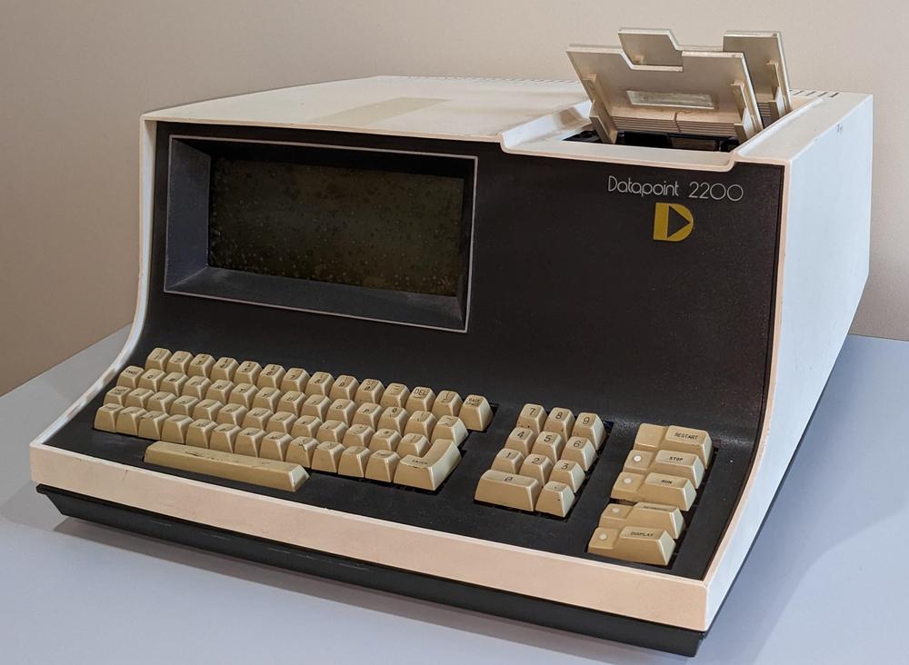
In the late 1960s, 80-column IBM punch cards were the primary way of entering data into computers, although CRT terminals were growing in popularity. The Datapoint 2200 was designed as a low-cost terminal that could replace a keypunch, with a squat CRT display the size of a punch card. By putting some processing power into the Datapoint 2200, it could perform data validation and other tasks, making data entry more efficient. Even though the Datapoint 2200 was typically used as an intelligent terminal, it was really a desktop minicomputer with a "unique combination of powerful computer, display, and dual cassette drives." Although now mostly forgotten, the Datapoint 2200 was the origin of the 8-bit microprocessor, as I'll explain below.
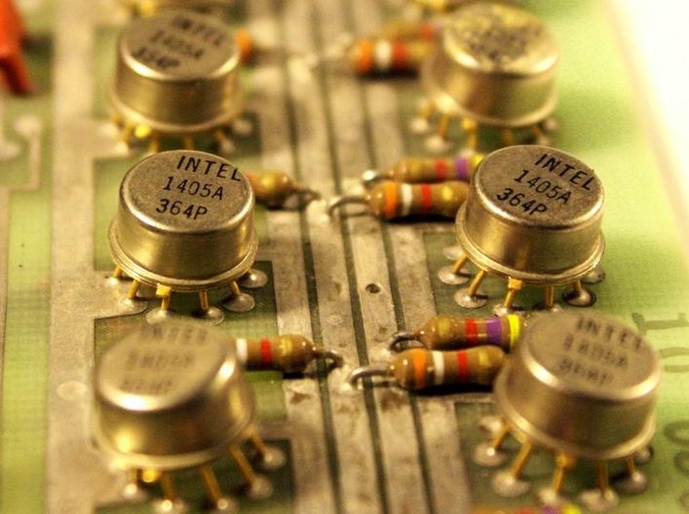
The memory storage of the Datapoint 2200 had a large impact on its architecture and thus the architecture of today's computers. In the 1960s and early 1970s, magnetic core memory was the dominant form of computer storage. It consisted of tiny ferrite rings, threaded into grids, with each ring storing one bit. Magnetic core storage was bulky and relatively expensive, though. Semiconductor RAM was new and very expensive; Intel's first product in 1969 was a RAM chip called the 3101, which held just 64 bits and cost $99.50. To minimize storage costs, the Datapoint 2200 used an alternative: MOS shift-register memory. The Intel 1405 shift-register memory chip provided much more storage than RAM chips at a much lower cost (512 bits for $13.30).1
The big problem with shift-register memory is that it is sequential: the bits come out one at a time, in the same order you put them in. This wasn't a problem when executing instructions sequentially, since the memory provided each instruction as it was needed. For a random access, though, you need to wait until the bits circulate around and you get the one you want, which is very slow. To minimize the number of memory accesses, the Datapoint 2200 had seven registers, a relatively large number of registers for the time.2 The registers were called A, B, C, D, E, H, and L, and these names had a lasting impact on Intel processors.
Another consequence of shift-register memory was that the Datapoint 2200 was a serial computer, operating on one bit at a time as the shift-register memory provided it, using a 1-bit ALU. To handle arithmetic operations, the ALU needed to start with the lowest bit so it could process carries. Likewise, a 16-bit value (such as a jump target) needed to start with the lowest bit. This resulted in a little-endian architecture, with the low byte first. The little-endian architecture has remained in Intel processors to the present.
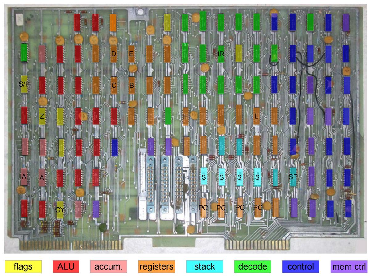
Since the Datapoint 2200 was designed before the creation of the microprocessor, its processor was built from a board of TTL chips (as was typical for minicomputers at the time).
The diagram below shows the processor board with the chips categorized by function.
The board has a separate chip for each 8-bit register (B, C, D, etc.) and separate chips for control flags (Z, carry, etc.).
The Arithmetic/Logic Unit (ALU) takes about 18 chips, while instruction decoding is another 18 chips.
Because every feature required more chips, the designers of the Datapoint 2200 were strongly motivated to make
the instruction set as simple as possible.
This was necessary since
the Datapoint 2200 was a low-cost device, renting for just $148 a month.
In contrast, the popular PDP-8 minicomputer rented for $500 a month.
One way that the Datapoint 2200 simplified the hardware was by creating a large set of instructions by combining simpler pieces in an orthogonal way. For instance, the Datapoint 2200 has 64 ALU instructions that apply one of eight ALU operations to one of the eight registers. This requires a small amount of hardware—eight ALU circuits and a circuit to select the register—but provides a large number of instructions. Another example is the register-to-register move instructions. Specifying one of eight source registers and one of eight destination registers provides a large, flexible set of instructions to move data.
The Datapoint 2200's instruction format was designed around this principle, with groups of three bits specifying a
register. A common TTL chip could decode the group of three bits and activate the desired circuit.3
For instance, a data move instruction had the bit pattern 11DDDSSS to move a byte from the specified source (SSS) to the specified destination (DDD).
(Note that this bit pattern maps onto three octal digits very nicely since the source and destination are separate digits.4)
One unusual feature of the Datapoint instruction set is that a memory access was just like a register access.
That is, an instruction could specify one of the seven physical registers or could specify a memory access (M),
using the identical instruction format.
One consequence of this is that you couldn't include a memory address in an instruction.
Instead, memory could only be accessed by first loading the address into the H and L registers, which held the high and
low byte of the address respectively.5
This is very unusual and inconvenient, since a memory access took three instructions: two to load the H and L registers and one to access memory as the M "register".
The advantage was that it simplified the instruction set and the decoding logic, saving chips and thus reducing
the system cost.
This decision also had lasting impact on Intel processors and how they access memory.
The table below shows the Datapoint 2200's instruction set in an octal table showing the 256 potential opcodes.6
I have roughly classified the instructions as arithmetic/logic (purple), control-flow (blue), data movement (green),
input/output (orange), and miscellaneous (yellow).
Note how the orthogonal instruction format produces large blocks of related instructions.
The instructions in the lower right (green) load (L) a value from a source to a destination.
(The no-operation NOP and HALT instructions are special cases.7)
In the upper-left are Load operations (LA, etc.) that use an "immediate" byte, a data byte that follows the instruction.
They use the same DDD code to specify the destination register, reusing that circuitry.
| 0 | 1 | 2 | 3 | 4 | 5 | 6 | 7 | 0 | 1 | 2 | 3 | 4 | 5 | 6 | 7 | |
|---|---|---|---|---|---|---|---|---|---|---|---|---|---|---|---|---|
| 0 | HALT | HALT | SLC | RFC | AD | LA | RETURN | JFC | INPUT | CFC | JMP | CALL | ||||
| 1 | SRC | RFZ | AC | LB | JFZ | CFZ | ||||||||||
| 2 | RFS | SU | LC | JFS | EX ADR | CFS | EX STATUS | EX DATA | EX WRITE | |||||||
| 3 | RFP | SB | LD | JFP | EX COM1 | CFP | EX COM2 | EX COM3 | EX COM4 | |||||||
| 4 | RTC | ND | LE | JTC | CTC | |||||||||||
| 5 | RTZ | XR | LH | JTZ | EX BEEP | CTZ | EX CLICK | EX DECK1 | EX DECK2 | |||||||
| 6 | RTS | OR | LL | JTS | EX RBK | CTS | EX WBK | EX BSP | ||||||||
| 7 | RTP | CP | JTP | EX SF | CTP | EX SB | EX REWND | EX TSTOP | ||||||||
| 0 | ADA | ADB | ADC | ADD | ADE | ADH | ADL | ADM | NOP | LAB | LAC | LAD | LAE | LAH | LAL | LAM |
| 1 | ACA | ACB | ACC | ACD | ACE | ACH | ACL | ACM | LBA | LBB | LBC | LBD | LBE | LBH | LBL | LBM |
| 2 | SUA | SUB | SUC | SUD | SUE | SUH | SUL | SUM | LCA | LCB | LCC | LCD | LCE | LCH | LCL | LCM |
| 3 | SBA | SBB | SBC | SBD | SBE | SBH | SBL | SBM | LDA | LDB | LDC | LDD | LDE | LDH | LDL | LDM |
| 4 | NDA | NDB | NDC | NDD | NDE | NDH | NDL | NDM | LEA | LEB | LEC | LED | LEE | LEH | LEL | LEM |
| 5 | XRA | XRB | XRC | XRD | XRE | XRH | XRL | XRM | LHA | LHB | LHC | LHD | LHE | LHH | LHL | LHM |
| 6 | ORA | ORB | ORC | ORD | ORE | ORH | ORL | ORM | LLA | LLB | LLC | LLD | LLE | LLH | LLL | LLM |
| 7 | CPA | CPB | CPC | CPD | CPE | CPH | CPL | CPM | LMA | LMB | LMC | LMD | LME | LMH | LML | HALT |
The lower-left quadrant (purple) has the bulk of the ALU instructions.
These instructions have a regular, orthogonal structure making the instructions easy to decode: each row specifies the operation while each column
specifies the source.
This is due to the instruction structure:
eight bits in the pattern 10AAASSS, where the AAA bits specified the
ALU operation and the SSS bits specified the register source.
The three-bit ALU code specifies the operations
Add, Add with Carry, Subtract, Subtract with Borrow, logical AND, logical XOR, logical OR,
and Compare.
This list is important because it defined the fundamental ALU operations for later Intel processors.8
In the upper-left are ALU operations that use an "immediate" byte.
These instructions use the same AAA bit pattern to select the ALU operation, reusing the decoding hardware.
Finally, the shift instructions SLC and SRC are implemented as special cases outside the pattern.
The upper columns contain conditional instructions in blue—Return, Jump, and Call.
The eight conditions test the four status flags (Carry, Zero, Sign, and Parity) for either True or False.
(For example, JFZ Jumps if the Zero flag is False.)
A 3-bit field selects the condition, allowing it to be easily decoded in hardware.
The parity flag is somewhat unusual because parity is surprisingly expensive to compute in hardware,
but because the Datapoint 2200 operated as a terminal, parity computation was important.
The Datapoint 2200 has an input instruction as well as many output instructions for a variety of specific hardware tasks
(orange, labeled EX for external).
Typical operations are STATUS to get I/O status, BEEP and CLICK to make sound, and REWIND to rewind the tape.
As a result of this decision to use separate I/O instructions, Intel processors still use I/O instructions operating in
an I/O space, different from processors such as the MOS 6502 and the Motorola 68000 that used memory-mapped I/O.
To summarize, the Datapoint 2200 has a fairly large number of instructions, but they are generated from about a dozen simple patterns that are easy to decode.9 By combining orthogonal bit fields (e.g. 8 ALU operations multiplied by 8 source registers), 64 instructions can be generated from one underlying pattern.
Intel 8008
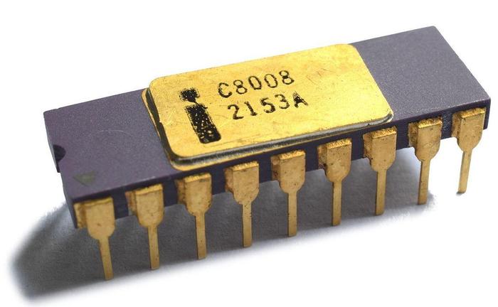
The Intel 8008 was created as a clone of the Datapoint 2200 processor.10 Around the end of 1969, the Datapoint company talked with Intel and Texas Instruments about the possibility of replacing the processor board with a single chip. Even though the microprocessor didn't exist at this point, both companies said they could create such a chip. Texas Instruments was first with a chip called the TMX 1795 that they advertised as a "CPU on a chip". Slightly later, Intel produced the 8008 microprocessor. Both chips copied the Datapoint 2200's instruction set architecture with minor changes.
By the time the chips were completed, however, the Datapoint corporation had lost interest in the chips. They were designing a much faster version of the Datapoint 2200 with improved TTL chips (including the well-known 74181 ALU chip). Even the original Datapoint 2200 model was faster than the Intel 8008 processor, and the Version II was over 5 times faster,11 so moving to a single-chip processor would be a step backward.
Texas Instruments unsuccessfully tried to find a customer for their TMX 1795 chip and ended up abandoning the chip. Intel, however, marketed the 8008 as an 8-bit microprocessor, essentially creating the microprocessor industry. In my view, Intel's biggest innovation with the microprocessor wasn't creating a single-chip CPU, but creating the microprocessor as a product category: a general-purpose processor along with everything customers needed to take advantage of it. Intel put an enormous amount of effort into making microprocessors a success: from documentation and customer training to Intellec development systems, from support chips to software tools such as assemblers, compilers, and operating systems.
The table below shows the opcodes of the 8008.
For the most part, the 8008 copies the Datapoint 2200, with identical instructions that have identical opcodes (in color).
There are a few additional instructions (shown in white), though.
Intel Designer Ted Hoff realized that increment and decrement instructions (IN and DC) would be very useful for loops.
There are two additional bit rotate instructions (RAL and RAR) as well as the "missing" LMI (Load Immediate to Memory)
instruction.
The RST (restart) instructions act as short call instructions to fixed addresses for
interrupt handling.
Finally, the 8008 turned the Datapoint 2200's device-specific I/O instructions into 32 generic I/O instructions.
| 0 | 1 | 2 | 3 | 4 | 5 | 6 | 7 | 0 | 1 | 2 | 3 | 4 | 5 | 6 | 7 | |
|---|---|---|---|---|---|---|---|---|---|---|---|---|---|---|---|---|
| 0 | HLT | HLT | RLC | RFC | ADI | RST 0 | LAI | RET | JFC | INP 0 | CFC | INP 1 | JMP | INP 2 | CAL | INP 3 |
| 1 | INB | DCB | RRC | RFZ | ACI | RST 1 | LBI | JFZ | INP 4 | CFZ | INP 5 | INP 6 | INP 7 | |||
| 2 | INC | DCC | RAL | RFS | SUI | RST 2 | LCI | JFS | OUT 8 | CFS | OUT 9 | OUT 10 | OUT 11 | |||
| 3 | IND | DCD | RAR | RFP | SBI | RST 3 | LDI | JFP | OUT 12 | CFP | OUT 13 | OUT 14 | OUT 15 | |||
| 4 | INE | DCE | RTC | NDI | RST 4 | LEI | JTC | OUT 16 | CTC | OUT 17 | OUT 18 | OUT 19 | ||||
| 5 | INH | DCH | RTZ | XRI | RST 5 | LHI | JTZ | OUT 20 | CTZ | OUT 21 | OUT 22 | OUT 23 | ||||
| 6 | INL | DCL | RTS | ORI | RST 6 | LLI | JTS | OUT 24 | CTS | OUT 25 | OUT 26 | OUT 27 | ||||
| 7 | RTP | CPI | RST 7 | LMI | JTP | OUT 28 | CTP | OUT 29 | OUT 30 | OUT 31 | ||||||
| 0 | ADA | ADB | ADC | ADD | ADE | ADH | ADL | ADM | NOP | LAB | LAC | LAD | LAE | LAH | LAL | LAM |
| 1 | ACA | ACB | ACC | ACD | ACE | ACH | ACL | ACM | LBA | LBB | LBC | LBD | LBE | LBH | LBL | LBM |
| 2 | SUA | SUB | SUC | SUD | SUE | SUH | SUL | SUM | LCA | LCB | LCC | LCD | LCE | LCH | LCL | LCM |
| 3 | SBA | SBB | SBC | SBD | SBE | SBH | SBL | SBM | LDA | LDB | LDC | LDD | LDE | LDH | LDL | LDM |
| 4 | NDA | NDB | NDC | NDD | NDE | NDH | NDL | NDM | LEA | LEB | LEC | LED | LEE | LEH | LEL | LEM |
| 5 | XRA | XRB | XRC | XRD | XRE | XRH | XRL | XRM | LHA | LHB | LHC | LHD | LHE | LHH | LHL | LHM |
| 6 | ORA | ORB | ORC | ORD | ORE | ORH | ORL | ORM | LLA | LLB | LLC | LLD | LLE | LLH | LLL | LLM |
| 7 | CPA | CPB | CPC | CPD | CPE | CPH | CPL | CPM | LMA | LMB | LMC | LMD | LME | LMH | LML | HLT |
Intel 8080
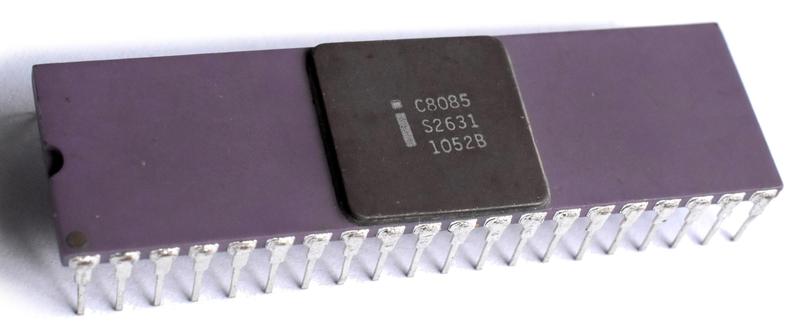
The 8080 improved the 8008 in many ways, focusing on speed and ease of use, and resolving customer issues with the 8008.12 Customers had criticized the 8008 for its small memory capacity, low speed, and difficult hardware interfacing. The 8080 increased memory capacity from 16K to 64K and was over an order of magnitude faster than the 8008. The 8080 also moved to a 40-pin package that made interfacing easier, but the 8080 still required a large number of support chips to build a working system.
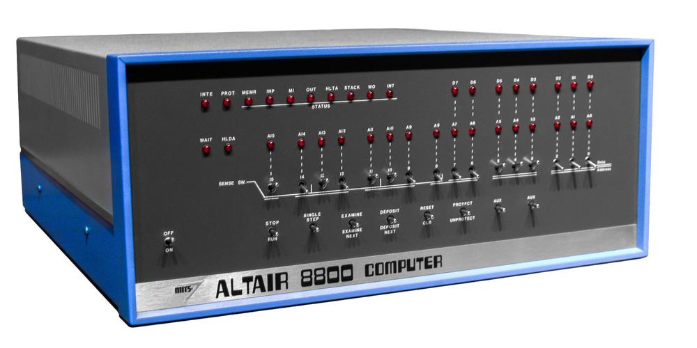
Although the 8080 was widely used in embedded systems, it is more famous for its use in the first generation of home computers, boxes such as the Altair and IMSAI. Famed chip designer Federico Faggin said that the 8080 really created the microprocessor; the 4004 and 8008 suggested it, but the 8080 made it real.13
The table below shows the instruction set for the 8080.
The 8080 was designed to be compatible with 8008 assembly programs after a simple translation process;
the instructions have been shifted around and the names have changed.15
The instructions from the Datapoint 2200 (colored) form the majority of the 8080's instruction set.
The instruction set was expanded by adding some 16-bit support, allowing register pairs (BC, DE, HL) to be used as 16-bit registers for
double add, 16-bit increment and decrement, and 16-bit memory transfers.
Many of the new instructions in the 8080 may seem like contrived special cases—
for example, SPHL (Load SP from HL) and XCHG (Exchange DE and HL)—
but they made accesses to memory easier.
The I/O instructions from the 8008 have been condensed to just IN and OUT, opening up room for new instructions.
| 0 | 1 | 2 | 3 | 4 | 5 | 6 | 7 | 0 | 1 | 2 | 3 | 4 | 5 | 6 | 7 | |
|---|---|---|---|---|---|---|---|---|---|---|---|---|---|---|---|---|
| 0 | NOP | LXI B | STAX B | INX B | INR B | DCR B | MVI B | RLC | MOV B,B | MOV B,C | MOV B,D | MOV B,E | MOV B,H | MOV B,L | MOV B,M | MOV B,A |
| 1 | DAD B | LDAX B | DCX B | INR C | DCR C | MVI C | RRC | MOV C,B | MOV C,C | MOV C,D | MOV C,E | MOV C,H | MOV C,L | MOV C,M | MOV C,A | |
| 2 | LXI D | STAX D | INX D | INR D | DCR D | MVI D | RAL | MOV D,B | MOV D,C | MOV D,D | MOV D,E | MOV D,H | MOV D,L | MOV D,M | MOV D,A | |
| 3 | DAD D | LDAX D | DCX D | INR E | DCR E | MVI E | RAR | MOV E,B | MOV E,C | MOV E,D | MOV E,E | MOV E,H | MOV E,L | MOV E,M | MOV E,A | |
| 4 | LXI H | SHLD | INX H | INR H | DCR H | MVI H | DAA | MOV H,B | MOV H,C | MOV H,D | MOV H,E | MOV H,H | MOV H,L | MOV H,M | MOV H,A | |
| 5 | DAD H | LHLD | DCX H | INR L | DCR L | MVI L | CMA | MOV L,B | MOV L,C | MOV L,D | MOV L,E | MOV L,H | MOV L,L | MOV L,M | MOV L,A | |
| 6 | LXI SP | STA | INX SP | INR M | DCR M | MVI M | STC | MOV M,B | MOV M,C | MOV M,D | MOV M,E | MOV M,H | MOV M,L | HLT | MOV M,A | |
| 7 | DAD SP | LDA | DCX SP | INR A | DCR A | MVI A | CMC | MOV A,B | MOV A,C | MOV A,D | MOV A,E | MOV A,H | MOV A,L | MOV A,M | MOV A,A | |
| 0 | ADD B | ADD C | ADD D | ADD E | ADD H | ADD L | ADD M | ADD A | RNZ | POP B | JNZ | JMP | CNZ | PUSH B | ADI | RST 0 |
| 1 | ADC B | ADC C | ADC D | ADC E | ADC H | ADC L | ADC M | ADC A | RZ | RET | JZ | CZ | CALL | ACI | RST 1 | |
| 2 | SUB B | SUB C | SUB D | SUB E | SUB H | SUB L | SUB M | SUB A | RNC | POP D | JNC | OUT | CNC | PUSH D | SUI | RST 2 |
| 3 | SBB B | SBB C | SBB D | SBB E | SBB H | SBB L | SBB M | SBB A | RC | JC | IN | CC | SBI | RST 3 | ||
| 4 | ANA B | ANA C | ANA D | ANA E | ANA H | ANA L | ANA M | ANA A | RPO | POP H | JPO | XTHL | CPO | PUSH H | ANI | RST 4 |
| 5 | XRA B | XRA C | XRA D | XRA E | XRA H | XRA L | XRA M | XRA A | RPE | PCHL | JPE | XCHG | CPE | XRI | RST 5 | |
| 6 | ORA B | ORA C | ORA D | ORA E | ORA H | ORA L | ORA M | ORA A | RP | POP PSW | JP | DI | CP | PUSH PSW | ORI | RST 6 |
| 7 | CMP B | CMP C | CMP D | CMP E | CMP H | CMP L | CMP M | CMP A | RM | SPHL | JM | EI | CM | CPI | RST 7 |
The 8080 also moved the stack to external memory, rather than using an internal fixed special-purpose stack as in the 8008 and
Datapoint 2200.
This allowed PUSH and POP instructions to put register data on the stack.
Interrupt handling was also improved by adding
the Enable Interrupt and Disable Interrupt instructions (EI and DI).14
Intel 8085
The Intel 8085 was designed as a "mid-life kicker" for the 8080, providing incremental improvements while maintaining compatibility. From the hardware perspective, the 8085 was much easier to use than the 8080. While the 8080 required three voltages, the 8085 required a single 5-volt power supply (represented by the "5" in the part number). Moreover, the 8085 eliminated most of the support chips required with the 8080; a working 8085 computer could be built with just three chips. Finally, the 8085 provided additional hardware functionality: better interrupt support and serial I/O.
On the software side, the 8085 is curious: 12 instructions were added to the instruction set (finally using every opcode), but all but two were hidden and left undocumented.16 Moreover, the 8085 added two new condition codes, but these were also hidden. This situation occurred because the 8086 project started up in 1976, near the release of the 8085 chip. Intel wanted the 8086 to be compatible (to some extent) with the 8080 and 8085, but providing new instructions in the 8085 would make compatibility harder. It was too late to remove the instructions from the 8085 chip, so Intel did the next best thing and removed them from the documentation. These instructions are shown in red in the table below. Only the new SIM and RIM instructions were supported, necessary in order to use the 8085's new interrupt and serial I/O features.
| 0 | 1 | 2 | 3 | 4 | 5 | 6 | 7 | 0 | 1 | 2 | 3 | 4 | 5 | 6 | 7 | |
|---|---|---|---|---|---|---|---|---|---|---|---|---|---|---|---|---|
| 0 | NOP | LXI B | STAX B | INX B | INR B | DCR B | MVI B | RLC | MOV B,B | MOV B,C | MOV B,D | MOV B,E | MOV B,H | MOV B,L | MOV B,M | MOV B,A |
| 1 | DSUB | DAD B | LDAX B | DCX B | INR C | DCR C | MVI C | RRC | MOV C,B | MOV C,C | MOV C,D | MOV C,E | MOV C,H | MOV C,L | MOV C,M | MOV C,A |
| 2 | ARHL | LXI D | STAX D | INX D | INR D | DCR D | MVI D | RAL | MOV D,B | MOV D,C | MOV D,D | MOV D,E | MOV D,H | MOV D,L | MOV D,M | MOV D,A |
| 3 | RDEL | DAD D | LDAX D | DCX D | INR E | DCR E | MVI E | RAR | MOV E,B | MOV E,C | MOV E,D | MOV E,E | MOV E,H | MOV E,L | MOV E,M | MOV E,A |
| 4 | RIM | LXI H | SHLD | INX H | INR H | DCR H | MVI H | DAA | MOV H,B | MOV H,C | MOV H,D | MOV H,E | MOV H,H | MOV H,L | MOV H,M | MOV H,A |
| 5 | LDHI | DAD H | LHLD | DCX H | INR L | DCR L | MVI L | CMA | MOV L,B | MOV L,C | MOV L,D | MOV L,E | MOV L,H | MOV L,L | MOV L,M | MOV L,A |
| 6 | SIM | LXI SP | STA | INX SP | INR M | DCR M | MVI M | STC | MOV M,B | MOV M,C | MOV M,D | MOV M,E | MOV M,H | MOV M,L | HLT | MOV M,A |
| 7 | LDSI | DAD SP | LDA | DCX SP | INR A | DCR A | MVI A | CMC | MOV A,B | MOV A,C | MOV A,D | MOV A,E | MOV A,H | MOV A,L | MOV A,M | MOV A,A |
| 0 | ADD B | ADD C | ADD D | ADD E | ADD H | ADD L | ADD M | ADD A | RNZ | POP B | JNZ | JMP | CNZ | PUSH B | ADI | RST 0 |
| 1 | ADC B | ADC C | ADC D | ADC E | ADC H | ADC L | ADC M | ADC A | RZ | RET | JZ | RSTV | CZ | CALL | ACI | RST 1 |
| 2 | SUB B | SUB C | SUB D | SUB E | SUB H | SUB L | SUB M | SUB A | RNC | POP D | JNC | OUT | CNC | PUSH D | SUI | RST 2 |
| 3 | SBB B | SBB C | SBB D | SBB E | SBB H | SBB L | SBB M | SBB A | RC | SHLX | JC | IN | CC | JNK | SBI | RST 3 |
| 4 | ANA B | ANA C | ANA D | ANA E | ANA H | ANA L | ANA M | ANA A | RPO | POP H | JPO | XTHL | CPO | PUSH H | ANI | RST 4 |
| 5 | XRA B | XRA C | XRA D | XRA E | XRA H | XRA L | XRA M | XRA A | RPE | PCHL | JPE | XCHG | CPE | LHLX | XRI | RST 5 |
| 6 | ORA B | ORA C | ORA D | ORA E | ORA H | ORA L | ORA M | ORA A | RP | POP PSW | JP | DI | CP | PUSH PSW | ORI | RST 6 |
| 7 | CMP B | CMP C | CMP D | CMP E | CMP H | CMP L | CMP M | CMP A | RM | SPHL | JM | EI | CM | JK | CPI | RST 7 |
Intel 8086
Following the 8080, Intel intended to revolutionize microprocessors with a 32-bit "micro-mainframe", the iAPX 432. This extremely complex processor implemented objects, memory management, interprocess communication, and fine-grained memory protection in hardware. The iAPX 432 was too ambitious and the project fell behind schedule, leaving Intel vulnerable against competitors such as Motorola and Zilog. Intel quickly threw together a 16-bit processor as a stopgap until the iAPX 432 was ready; to show its continuity with the 8-bit processor line, this processor was called the 8086. The iAPX 432 ended up being one of the great disaster stories of modern computing and quietly disappeared.
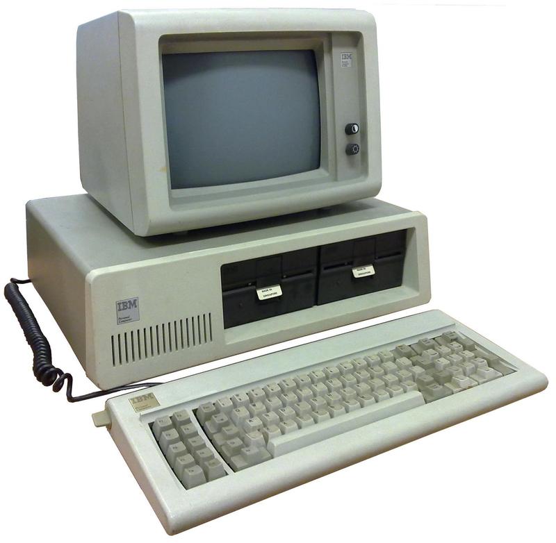
The "stopgap" 8086 processor, however, started the x86 architecture that changed the history of Intel. The 8086's victory was powered by the IBM PC, designed in 1981 around the Intel 8088, a variant of the 8086 with a cheaper 8-bit bus. The IBM PC was a rousing success, defining the modern computer and making Intel's fortune. Intel produced a succession of more powerful chips that extended the 8086: 286, 386, 486, Pentium, and so on, leading to the current x86 architecture.
The 8086 was a major change from the 8080/8085, jumping from an 8-bit architecture to a 16-bit architecture and expanding from 64K of memory to 1 megabyte. Nonetheless, the 8086's architecture is closely related to the 8080. The designers of the 8086 wanted it to be compatible with the 8080/8085, but the difference was too wide for binary compatibility or even assembly-language compatibility. Instead, the 8086 was designed so a program could translate 8080 assembly language to 8086 assembly language.17 To accomplish this, each 8080 register had a corresponding 8086 register and most 8080 instructions had corresponding 8086 instructions.
The 8086's instruction set was designed with a new concept, the "ModR/M" byte, which usually follows the opcode byte. The ModR/M byte specifies the memory addressing mode and the register (or registers) to use, allowing that information to be moved out of the opcode. For instance, where the 8080 had a quadrant of 64 instructions to move from register to register, the 8086 has a single move instruction, with the ModR/M byte specifying the particular instruction. (The move instruction, however, has variants to handle byte vs. word operations, moves to or from memory, and so forth, so the 8086 ends up with a few move opcodes.) The ModR/M byte preserves the Datapoint 2200's concept of using the same instruction for memory and register operations, but allows a memory address to be provided in the instruction.
The 8086 also cleans up some of the historical baggage in the instruction set, freeing up space in the precious
256 opcodes for new instructions.
The conditional call and return instructions were eliminated, while the conditional jumps were expanded.
The 8008's RST (Restart) instructions were eliminated, replaced by interrupt vectors.
The 8086 extended its registers to 16 bits and added several new registers.
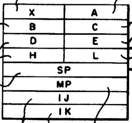
An Intel patent (below) shows that the 8086's registers were originally called A, B, C, D, E, H, and L,
matching the Datapoint 2200.
The A register was extended to the 16-bit XA register, while the
BC, DE, and HL registers were used unchanged.
When the 8086 was released, these registers were renamed to AX, CX, DX, and BX respectively.18
In particular, the HL register was renamed to BX; this is why BX can specify a memory address in the ModR/M byte, but
AX, CX, and DX can't.
The table below shows the 8086's instruction set, with "b", "w", and "i" indicating byte (8-bit), word (16-bit), and immediate instructions. The Datapoint 2200 instructions (colored) are all still supported. The number of Datapoint instructions looks small because the ModR/M byte collapses groups of old opcodes into a single new one. This opened up space in the opcode table, though, allowing the 8086 to have many new instructions as well as 16-bit instructions.19
| 0 | 1 | 2 | 3 | 4 | 5 | 6 | 7 | 0 | 1 | 2 | 3 | 4 | 5 | 6 | 7 | |
|---|---|---|---|---|---|---|---|---|---|---|---|---|---|---|---|---|
| 0 | ADD b | ADD w | ADD b | ADD w | ADD bi | ADD wi | PUSH ES | POP ES | INC AX | INC CX | INC DX | INC BX | INC SP | INC BP | INC SI | INC DI |
| 1 | OR b | OR w | OR b | OR w | OR bi | OR wi | PUSH CS | DEC AX | DEC CX | DEC DX | DEC BX | DEC SP | DEC BP | DEC SI | DEC DI | |
| 2 | ADC b | ADC w | ADC b | ADC w | ADC bi | ADC wi | PUSH SS | POP SS | PUSH AX | PUSH CX | PUSH DX | PUSH BX | PUSH SP | PUSH BP | PUSH SI | PUSH DI |
| 3 | SBB b | SBB w | SBB b | SBB w | SBB bi | SBB wi | PUSH DS | POP DS | POP AX | POP CX | POP DX | POP BX | POP SP | POP BP | POP SI | POP DI |
| 4 | AND b | AND w | AND b | AND w | AND bi | AND wi | ES: | DAA | ||||||||
| 5 | SUB b | SUB w | SUB b | SUB w | SUB bi | SUB wi | CS: | DAS | ||||||||
| 6 | XOR b | XOR w | XOR b | XOR w | XOR bi | XOR wi | SS: | AAA | JO | JNO | JB | JNB | JZ | JNZ | JBE | JA |
| 7 | CMP b | CMP w | CMP b | CMP w | CMP bi | CMP wi | DS: | AAS | JS | JNS | JPE | JPO | JL | JGE | JLE | JG |
| 0 | GRP1 b | GRP1 w | GRP1 b | GRP1 w | TEST b | TEST w | XCHG b | XCHG w | RET | RET | LES | LDS | MOV b | MOV w | ||
| 1 | MOV b | MOV w | MOV b | MOV w | MOV sr | LEA | MOV sr | POP | RETF | RETF | INT 3 | INT | INTO | IRET | ||
| 2 | NOP | XCHG CX | XCHG DX | XCHG BX | XCHG SP | XCHG BP | XCHG SI | XCHG DI | Shift b | Shift w | Shift b | Shift w | AAM | AAD | XLAT | |
| 3 | CBW | CWD | CALL | WAIT | PUSHF | POPF | SAHF | LAHF | ESC 0 | ESC 1 | ESC 2 | ESC 3 | ESC 4 | ESC 5 | ESC 6 | ESC 7 |
| 4 | MOV AL,M | MOV AX,M | MOV M,AL | MOV M,AX | MOVS b | MOVS w | CMPS b | CMPS w | LOOPNZ | LOOPZ | LOOP | JCXZ | IN b | IN w | OUT b | OUT w |
| 5 | TEST b | TEST w | STOS b | STOS w | LODS b | LODS w | SCAS b | SCAS w | CALL | JMP | JMP | JMP | IN b | IN w | OUT b DX | OUT w DX |
| 6 | MOV AL,i | MOV CL,i | MOV DL,i | MOV BL,i | MOV AH,i | MOV CH,i | MOV DH,i | MOV BH,i | LOCK | REPNZ | REPZ | HLT | CMC | GRP3a | GRP3b | |
| 7 | MOV AX,i | MOV CX,i | MOV DX,i | MOV BX,i | MOV SP,i | MOV BP,i | MOV SI,i | MOV DI,i | CLC | STC | CLI | STI | CLD | STD | GRP4 | GRP5 |
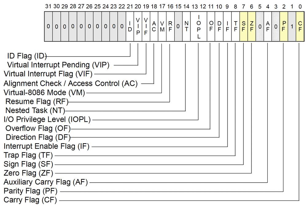
The 8086 has a 16-bit flags register, shown below, but the low byte remained compatible with the 8080. The four highlighted flags (sign, zero, parity, and carry) are the ones originating in the Datapoint 2200.
Modern x86 and x86-64
The modern x86 architecture has extended the 8086 to a 32-bit architecture (IA-32) and a 64-bit architecture (x86-6420), but the Datapoint features remain. At startup, an x86 processor runs in "real mode", which operates like the original 8086. More interesting is 64-bit mode, which has some major architectural changes. In 64-bit mode, the 8086's general-purpose registers are extended to sixteen 64-bit registers (and soon to be 32 registers). However, the original Datapoint registers are special and can still be accessed as byte registers within the corresponding 64-bit register; these are highlighted in the table below.21
The flag register of the 8086 was extended to 32 bits or 64 bits in x86. As the diagram below shows, the original Datapoint 2200 status flags are still there (highlighted in yellow).
The instruction set in x86 has been extended from the 8086, mostly through prefixes, but
the instructions from the Datapoint 2200 are still there.
The ModR/M byte was changed in 32-bit mode so the BX (originally HL) register is no longer special
when accessing memory (although it's still special with 16-bit addressing, until Intel removes that in the
upcoming x86-S simplification.)
I/O ports still exist in x86, although they are viewed as more of a legacy feature: modern I/O devices
typically use memory-mapped I/O instead of I/O ports.
To summarize, fifty years later, x86-64 is slowly moving away from some of the Datapoint 2200 features, but they are still there.
Conclusions
The modern x86 architecture is descended from the Datapoint 2200's architecture. Because there is backward-compatibility at each step, you should theoretically be able to take a Datapoint 2200 binary, disassemble it to 8008 assembly, automatically translate it to 8080 assembly, automatically convert it to 8086 assembly, and then run it on a modern x86 processor. (The I/O devices would be different and cause trouble, of course.)
The Datapoint 2200's complete instruction set, its flags, and its little-endian architecture have persisted into current processors. This shows the critical importance of backward compatibility to customers. While Intel keeps attempting to create new architectures (iAPX 432, i960, i860, Itanium), customers would rather stay on a compatible architecture. Remarkably, Intel has managed to move from 8-bit computers to 16, 32, and 64 bits, while keeping systems mostly compatible. As a result, design decisions made for the Datapoint 2200 over 50 years ago are still impacting modern computers. Will processors still have the features of the Datapoint 2200 another fifty years from now? I wouldn't be surprised.22
Thanks to Joe Oberhauser for suggesting this topic. I plan to write more on the 8086, so follow me on Twitter @kenshirriff or RSS for updates. I've also started experimenting with Mastodon recently as @[email protected] so you can follow me there too.
Notes and references
-
Shift-register memory was also used in the TV Typewriter (1973) and the display storage of the Apple I (1976). However, dynamic RAM (DRAM) rapidly dropped in price, making shift-register memory obsolete by the mid 1970s. (I wrote about the Intel 1405 shift register memory in detail in this article.) ↩
-
For comparison, the popular PDP-8 minicomputer had just two main registers: the accumulator and a multiplier-quotient register; instructions typically operated on the accumulator and a memory location. The Data General Nova, a minicomputer released in 1969, had four accumulator / index registers. Mainframes generally had many more registers; the IBM System/360 (1964), for instance, had 16 general registers and four floating-point registers. ↩
-
On the hardware side, instructions were decoded with BCD-to-decimal decoder chips (type 7442). These decoders normally decoded a 4-bit BCD value into one of 10 output lines. In the Datapoint 2200, they decoded a 3-bit value into one of 8 output lines, and the other two lines were ignored. This allowed the high-bit line to be used as a selection line; if it was set, none of the 8 outputs would be active. ↩
-
These bit patterns map cleanly onto octal, so the opcodes are clearest when specified in octal. This octal structure has persisted in Intel processors including modern x86 processors. Unfortunately, Intel invariably specifies the opcodes in hexadecimal rather than octal, which obscures the underlying structure. This structure is described in detail in The 80x86 is an Octal Machine. ↩
-
It is unusual for an instruction set to require memory addresses to be loaded into a register in order to access memory. This technique was common in microcode, where memory addresses were loaded into the Memory Address Register (
MAR). As pwg pointed out, the CDC mainframes (e.g. 6600) had special address registers; when you changed an address register, the specified memory location was read or written to the corresponding operand register automatically.At first, I thought that serial memory might motivate the use of an address register, but I don't think there's a connection. Most likely, the Datapoint 2200 used these techniques to create a simple, orthogonal instruction set that was easy to decode, and they weren't particularly concerned with performance. ↩
-
The instruction tables in this article are different from most articles, because I use octal instead of hexadecimal. (Displaying an octal-based instruction in a hexadecimal table obscures much of the underlying structure.) To display the table in octal, I break it into four quadrants based on the top octal digit of a three-digit opcode: 0, 1, 2, or 3. The digit 0-7 along the left is the middle octal digit and the digit along the top is the low octal digit. ↩
-
The regular pattern of Load instructions is broken by the
NOPandHALTinstructions. All the register-to-register load instructions along the diagonal accomplish nothing since they move a register to itself, but only the first one is explicitly calledNOP. Moving a memory location to itself doesn't make sense, so its opcode is assigned theHALTinstruction. Note that the all-0's opcode and the all-1's opcode are bothHALTinstructions. This is useful since it can stop execution if the program tries executing uninitialized memory. ↩ -
You might think that Datapoint and Intel used the same ALU operations simply because they are the obvious set of 8 operations. However, if you look at other processors around that time, they use a wide variety of ALU operations. Similarly, the status flags in the Datapoint 2200 aren't the obvious set; systems with four flags typically used Sign, Carry, Zero, and Overflow (not Parity). Parity is surprisingly expensive to implement on a standard processor, but (as Philip Freidin pointed out) parity is cheap on a serial processor like the Datapoint 2200. Intel processors didn't provide an Overflow flag until the 8086; even the 8080 didn't have it although the Motorola 6800 and MOS 6502 did. The 8085 implemented an overflow flag (
V) but it was left undocumented. ↩ -
You might wonder if the Datapoint 2200 (and 8008) could be considered RISC processors since they have simple, easy-to-decode instruction sets. I think it is a mistake to try to wedge every processor into the RISC or CISC categories (Reduced Instruction Set Computer or Complex Instruction Set Computer). In particular, the Datapoint 2200 wasn't designed with the RISC philosophy (make a processor more powerful by simplifying the instruction set), its instruction set architecture is very different from RISC chips, and its implementation is different from RISC chips. Similarly, it wasn't designed with a CISC philosophy (make a processor more powerful by narrowing the semantic gap with high-level languages) and it doesn't look like a CISC chip.
So where does that leave the Datapoint 2200? In "RISC: Back to the future?", famed computer architect Gordon Bell uses the term MISC (Minimal Instruction Set Computer) to describe the architecture of simple, early computers and microprocessors such as the Manchester Mark I (1948), the PDP-8 minicomputer (1966), and the Intel 4004 (1971). Computer architecture evolved from these early hardwired "simple computers" to microprogrammed processors, processors with cache, and hardwired, pipelined processors. "Minimal Instruction Set Computer" seems like a good description of the Datapoint 2200, since it is about the smallest, simplest processor that could get the job done. ↩
-
Many people think that the Intel 8008 is an extension of the 4-bit Intel 4004 processor, but they are completely unrelated aside from the part numbers. The Intel 4004 is a 4-bit processor designed to implement a calculator for a company called Busicom. Its architecture is completely different from the 8008. In particular, the 4004 is a "Harvard architecture" system, with data storage and instruction storage completely separate. The 4004 also has a fairly strange instruction set, designed for calculators. For instance, it has a special instruction to convert a keyboard scan code to binary. The 4004 team and the 8008 team at Intel had many people in common, however, so the two chips have physical layouts (floorplans) that are very similar. ↩
-
In this article, I'm focusing on the Datapoint 2200 Version I. Any time I refer to the Datapoint 2200, I mean the version I specifically. The Version II has an expanded instruction set, but it was expanded in an entirely different direction from the Intel 8080, so it's not relevant to this post. The Version II is interesting, however, since it provides a perspective of how the Intel 8080 could have developed in an "alternate universe". ↩
-
Federico Faggin wrote The Birth of the Microprocessor in Byte Magazine, March 1992. This article describes in some detail the creation of the 8008 and 8080.
The Oral History of the 8080 discusses many of the problems with the 8008 and how the 8080 addressed them. (See page 4.) Masatoshi Shima, one of the architects of the 4004, described five problems with the 8008: It was slow because it used two clock cycles per state. It had no general-purpose stack and was weak with interrupts. It had limited memory and I/O space. The instruction set was primitive, with only 8-bit data, limited addressing, and a single address pointer register. Finally, the system bus required a lot of interface circuitry. (See page 7.) ↩
-
The 8080 is often said to be the "first truly usable microprocessor". Supposedly the source of this quote is Forgotten PC history, but the statement doesn't appear there. I haven't been able to find the original source of this statement, so let me know. In any case, I don't think that statement is particularly accurate, as the Motorola 6800 was "truly usable" and came out before the Intel 8080.
The 8080 was first in one important way, though: it was Intel's first microprocessor that was designed with feedback from customers. Both the 4004 and the 8008 were custom chips for a single company. The 8080, however, was based on extensive customer feedback about the flaws in the 8008 and what features customers wanted. The 8080 oral history discusses this in more detail. ↩
-
The 8008 was built with PMOS circuitry, while the 8080 was built with NMOS. This may seem like a trivial difference, but NMOS provided much superior performance. NMOS became the standard microprocessor technology until the rise of CMOS in the 1980s, combining NMOS and PMOS to dramatically reduce power consumption.
Another key hardware improvement was that the 8080 used a 40-pin package, compared to the 18-pin package of the 8008. Intel had long followed the "religion" of small 16-pin packages, and only reluctantly moved to 18 pins (as in the 8008). However, by the time the 8080 was introduced, Intel recognized the utility of industry-standard 40-pin packages. The additional pins made the 8080 much easier to interface to a system. Moreover, the 8080's 16-bit address bus supported four times the memory of the 8008's 14-bit address bus. (The 40-pin package was still small for the time; some companies used 50-pin or 64-pin packages for microprocessors.) ↩
-
The 8080 is not binary-compatible with the 8008 because almost all the instructions were shifted to different opcodes. One important but subtle change was that the 8 register/memory codes were reordered to start with
Binstead ofA. The motivation is that this gave registers in a 16-bit register pair (BC,DE, orHL) codes that differ only in the low bit. This makes it easier to specify a register pair with a two-bit code. ↩ -
Stan Mazor (one of the creators of the 4004 and 8080) explained that the 8085 removed 10 of the 12 new instructions because "they would burden the 8086 instruction set." Because the decision came near the 8085's release, they would "leave all 12 instructions on the already designed 8085 CPU chip, but document and announce only two of them" since modifying a CPU is hard but modifying a CPU's paper reference manual is easy.
Several of the Intel 8086 engineers provided a similar explanation in Intel Microprocessors: 8008 to 8086: While the 8085 provided the new
RIMandSIMinstructions, "several other instructions that had been contemplated were not made available because of the software ramifications and the compatibility constraints they would place on the forthcoming 8086."For more information on the 8085's undocumented instructions, see Unspecified 8085 op codes enhance programming. The two new condition flags were
V(2's complement overflow) andX5(underflow on decrement or overflow on increment). The opcodes wereDSUB(double (i.e. 16-bit) subtraction),ARHL(arithmetic shift right ofHL),RDEL(rotateDEleft through carry),LDHI(loadDEwithHLplus an immediate byte),LDSI(load DE withSPplus an immediate byte),RSTV(restart on overflow),LHLX(loadHLindirect throughDE),SHLX(storeHLindirect throughDE),JX5(jump onX5), andJNX5(jump on notX5). ↩ -
Conversion from 8080 assembly code to 8086 assembly code was performed with a tool called CONV86. Each line of 8080 assembly code was converted to the corresponding line (or sometimes a few lines) of 8086 assembly code. The program wasn't perfect, so it was expected that the user would need to do some manual editing. In particular, CONV86 couldn't handle self-modifying code, where the program changed its own instructions. (Nowadays, self-modifying code is almost never used, but it was more common in the 1970s in order to make code smaller and get more performance.) CONV86 also didn't handle the 8085's
RIMandSIMinstructions, recommending a rewrite if code used these instructions heavily.Writing programs in 8086 assembly code manually was better, of course, since the program could take advantage of the 8086's new features. Moreover, a program converted by CONV86 might be 25% larger, due to the 8086's use of two-byte instructions and inefficiencies in the conversion. ↩
-
This renaming is why the instruction set has the registers in the order
AX,CX,DX,BX, rather than in alphabetical order as you might expect. The other factor is that Intel decided thatAX,BX,CX, andDXcorresponded to Accumulator, Base, Count, and Data, so they couldn't assign the names arbitrarily. ↩ -
A few notes on how the 8086's instructions relate to the earlier machines, since the ModR/M byte and 8- vs. 16-bit instructions make things a bit confusing. For an instruction like
ADD, I have three 8-bit opcodes highlighted: an add to memory/register, an add from memory/register, and an immediate add. The neighboring unhighlighted opcodes are the corresponding 16-bit versions. Likewise, forMOV, I have highlighted the 8-bit moves to/from a register/memory. ↩ -
Since the x86's 32-bit architecture is called IA-32, you might expect that IA-64 would be the 64-bit architecture. Instead, IA-64 is the completely different architecture used in the ill-fated Itanium. IA-64 was supposed to replace IA-32, despite being completely incompatible. Since AMD was cut out of IA-64, AMD developed their own 64-bit extension of the existing x86 architecture and called it AMD64. Customers flocked to this architecture while the Itanium languished. Intel reluctantly copied the AMD64 architecture, calling it Intel 64. ↩
-
The x86 architecture allows byte access to certain parts of the larger registers (accessing
AL,AH, etc.) as well as word and larger accesses. These partial-width reads and writes to registers make the implementation of the processor harder due to register renaming. The problem is that writing to part of a register means that the register's value is a combination of the old and new values. The Register Alias Table in the P6 architecture deals with this by adding a size field to each entry. If you write a short value and then read a longer value, the pipeline stalls to figure out the right value. Moreover, some 16-bit code uses the two 8-bit parts of a register as independent registers. To support this, the Register Alias Table keeps separate entries for the high and low byte. (For details, see the book Modern Processor Design, in particular the chapter on Intel's P6 Microarchitecture.) The point of this is that obscure features of the Datapoint 2200 (such asHandLacting as a combined register) can cause implementation difficulties 50 years later. ↩ -
Some miscellaneous references: For a detailed history of the Datapoint 2200, see Datapoint: The Lost Story of the Texans Who Invented the Personal Computer Revolution. The 8008 oral history provides a lot of interesting information on the development of the 8008. For another look at the Datapoint 2200 and instruction sets, see Comparing Datapoint 2200, 8008, 8080 and Z80 Instruction Sets. ↩
