A close look at the 8086 processor's bus hold circuitry

The Intel 8086 microprocessor (1978) revolutionized computing by founding the x86 architecture that continues to this day. One of the lesser-known features of the 8086 is the "hold" functionality, which allows an external device to temporarily take control of the system's bus. This feature was most important for supporting the 8087 math coprocessor chip, which was an option on the IBM PC; the 8087 used the bus hold so it could interact with the system without conflicting with the 8086 processor.

This blog post explains in detail how the bus hold feature is implemented in the processor's logic. (Be warned that this post is a detailed look at a somewhat obscure feature.) I've also found some apparently undocumented characteristics of the 8086's hold acknowledge circuitry, designed to make signal transition faster on the shared control lines.

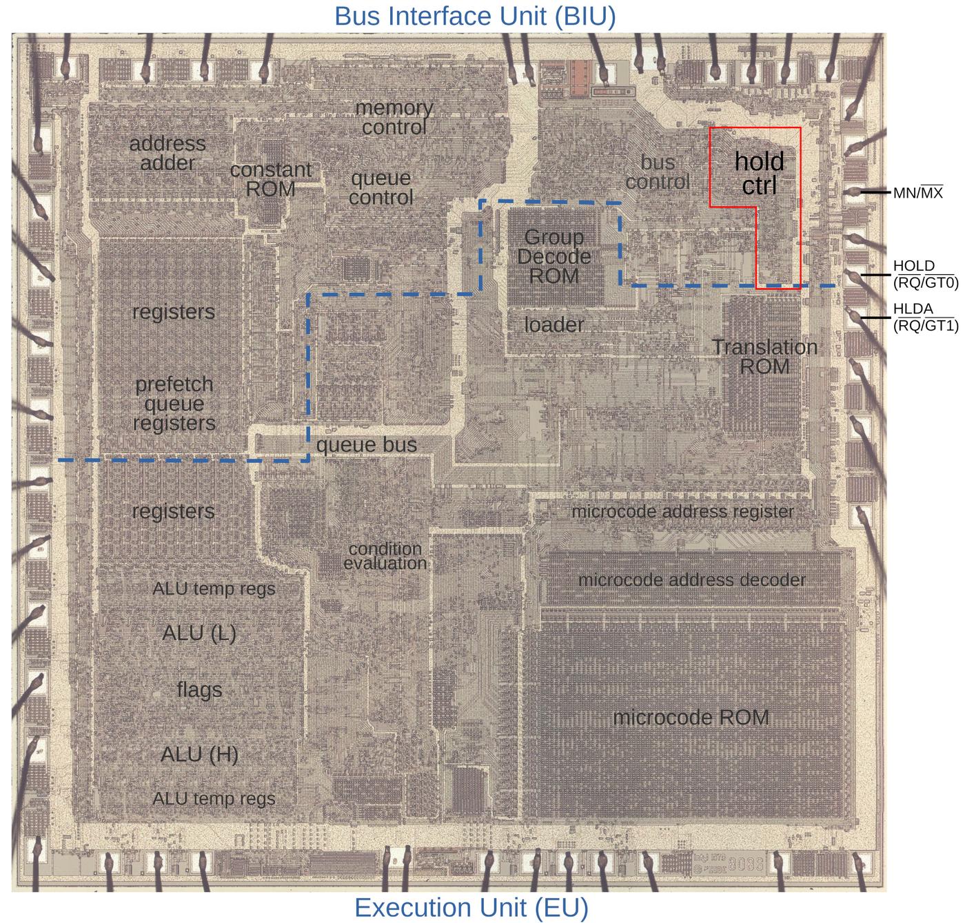
The die photo below shows the main functional blocks of the 8086 processor. In this image, the metal layer on top of the chip is visible, while the silicon and polysilicon underneath are obscured. The 8086 is partitioned into a Bus Interface Unit (upper) that handles bus traffic, and an Execution Unit (lower) that executes instructions. The two units operate mostly independently, which will turn out to be important. The Bus Interface Unit handles read and write operations as requested by the Execution Unit. The Bus Interface Unit also prefetches instructions that the Execution Unit uses when it needs them. The hold control circuitry is highlighted in the upper right; it takes a nontrivial amount of space on the chip. The square pads around the edge of the die are connected by tiny bond wires to the chip's 40 external pins. I've labeled the MN/MX, HOLD, and HLDA pads; these are the relevant signals for this post.

The 8086 die under the microscope, with the main functional blocks and relevant pins labeled. Click this image (or any other) for a larger version.

The 8086 die under the microscope, with the main functional blocks and relevant pins labeled. Click this image (or any other) for a larger version.

How bus hold works

In an 8086 system, the processor communicates with memory and I/O devices over a bus consisting of address and data lines along with various control signals. For high-speed data transfer, it is useful for an I/O device to send data directly to memory, bypassing the processor; this is called DMA (Direct Memory Access). Moreover, a co-processor such as the 8087 floating point unit may need to read data from memory. The bus hold feature supports these operations: it is a mechanism for the 8086 to give up control of the bus, letting another device use the bus to communicate with memory. Specifically, an external device requests a bus hold and the 8086 stops putting electrical signals on the bus and acknowledges the bus hold. The other device can now use the bus. When the other device is done, it signals the 8086, which then resumes its regular bus activity.

Most things in the 8086 are more complicated than you might expect, and the bus hold feature is no exception, largely due to the 8086's minimum and maximum modes. The 8086 can be designed into a system in one of two ways—minimum mode and maximum mode—that redefine the meanings of the 8086's external pins. Minimum mode is designed for simple systems and gives the control pins straightforward meanings such as indicating a read versus a write. Minimum mode provides bus signals that were similar to the earlier 8080 microprocessor, making migration to the 8086 easier. On the other hand, maximum mode is designed for sophisticated, multiprocessor systems and encodes the control signals to provide richer system information.

In more detail, minimum mode is selected if the MN/MX pin is wired high, while maximum mode is selected if the MN/MX pin is wired low. Nine of the chip's pins have different meanings depending on the mode, but only two pins are relevant to this discussion. In minimum mode, pin 31 has the function HOLD, while pin 30 has the function HLDA (Hold Acknowlege). In maximum mode, pin 31 has the function RQ/GT0', while pin 30 has the function RQ/GT1'.

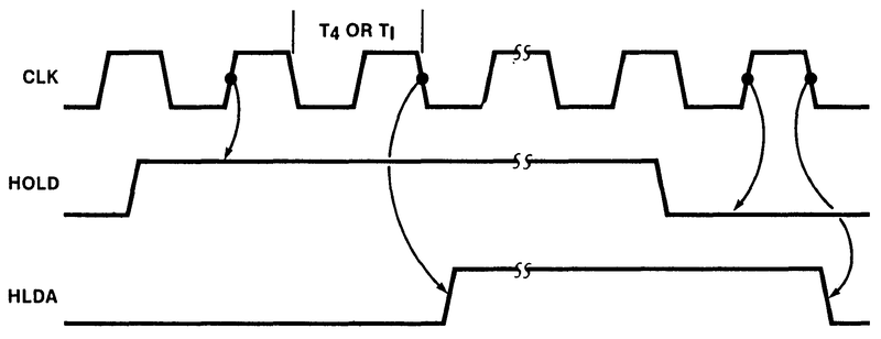
I'll start by explaining how a hold operation works in minimum mode. When an external device wants to use the bus, it pulls the HOLD pin high. At the end of the current bus cycle, the 8086 acknowledges the hold request by pulling HLDA high. The 8086 also puts its bus output pins into "tri-state" mode, in effect disconnecting them electrically from the bus. When the external device is done, it pulls HOLD low and the 8086 regains control of the bus. Don't worry about the details of the timing below; the key point is that a device pulls HOLD high and the 8086 responds by pulling HLDA high.

This diagram shows the HOLD/HLDA sequence. From iAPX 86,88 User's Manual, Figure 4-14.

This diagram shows the HOLD/HLDA sequence. From iAPX 86,88 User's Manual, Figure 4-14.

The 8086's maximum mode is more complex, allowing two other devices to share the bus by using a priority-based scheme. Maximum mode uses two bidirectional signals, RQ/GT0 and RQ/GT1.2 When a device wants to use the bus, it issues a pulse on one of the signal lines, pulling it low. The 8086 responds by pulsing the same line. When the device is done with the bus, it issues a third pulse to inform the 8086. The RQ/GT0 line has higher priority than RQ/GT1, so if two devices request the bus at the same time, the RQ/GT0 device wins and the RQ/GT1 device needs to wait.1 Keep in mind that the RQ/GT lines are bidirectional: the 8086 and the external device both use the same line for signaling.

This diagram shows the request/grant sequence. From iAPX 86,88 User's Manual, Figure 4-16.

This diagram shows the request/grant sequence. From iAPX 86,88 User's Manual, Figure 4-16.

The bus hold does not completely stop the 8086. The hold operation stops the Bus Interface Unit, but the Execution Unit will continue executing instructions until it needs to perform a read or write, or it empties the prefetch queue. Specifically, the hold signal blocks the Bus Interface Unit from starting a memory cycle and blocks an instruction prefetch from starting.

Bus sharing and the 8087 coprocessor

Probably the most common use of the bus hold feature was to support the Intel 8087 math coprocessor. The 8087 coprocessor greatly improved the performance of floating-point operations, making them up to 100 times faster. As well as floating-point arithmetic, the 8087 supported trigonometric operations, logarithms and powers. The 8087's architecture became part of later Intel processors, and the 8087's instructions are still a part of today's x86 computers.3

The 8087 had its own registers and didn't have access to the 8086's registers. Instead, the 8087 could transfer values to and from the system's main memory. Specifically, the 8087 used the RQ/GT mechanism (maximum mode) to take control of the bus if the 8087 needed to transfer operands to or from memory.4 The 8087 could be installed as an option on the original IBM PC, which is why the IBM PC used maximum mode.

The enable flip-flop

The circuit is built from six flip-flops. The flip-flops are a bit different from typical D flip-flops, so I'll discuss the flip-flop behavior before explaining the circuit.

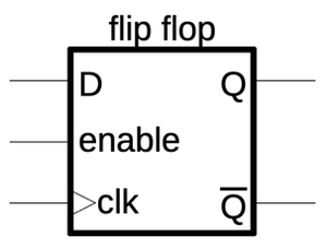
A flip-flop can store a single bit, 0 or 1. Flip flops are very important in the 8086 because they hold information (state) in a stable way, and they synchronize the circuitry with the processor's clock. A common type of flip-flop is the D flip-flop, which takes a data input (D) and stores that value. In an edge-triggered flip-flop, this storage happens on the edge when the clock changes state from low to high.5 (Except at this transition, the input can change without affecting the output.) The output is called Q, while the inverted output is called Q-bar.

The symbol for the D flip-flop with enable.

The symbol for the D flip-flop with enable.

Many of the 8086's flip-flops, including the ones in the hold circuit, have an "enable" input. When the enable input is high, the flip-flop records the D input, but when the enable input is low, the flip-flop keeps its previous value. Thus, the enable input allows the flip-flop to hold its value for more than one clock cycle. The enable input is very important to the functioning of the hold circuit, as it is used to control when the circuit moves to the next state.

How bus hold is implemented (minimum mode)

I'll start by explaining how the hold circuitry works in minimum mode. To review, in minimum mode the external device requests a hold through the HOLD input, keeping the input high for the duration of the request. The 8086 responds by pulling the hold acknowledge HLDA output high for the duration of the hold.

In minimum mode, only three of the six flip-flops are relevant. The diagram below is highly simplified to show the essential behavior. (The full schematic is in the footnotes.6) At the left is the HOLD signal, the request from the external device.

Simplified diagram of the circuitry for minimum mode.

Simplified diagram of the circuitry for minimum mode.

When a HOLD request comes in, the first flip-flop is activated, and remains activated for the duration of the request. The second flip-flop waits if any condition is blocking the hold request: a LOCK instruction, an unaligned memory access, or so forth. When the HOLD can proceed, the second flip-flop is enabled and it latches the request. The second flip-flop controls the internal hold signal, causing the 8086 to stop further bus activity. The third flip-flop is then activated when the current bus cycle (if any) completes; when it latches the request, the hold is "official". The third flip-flop drives the external HLDA (Hold Acknowledge) pin, indicating that the bus is free. This signal also clears the bus-enabled latch (elsewhere in the 8086), putting the appropriate pins into floating tri-state mode. The key point is that the flip-flops control the timing of the internal hold and the external HLDA, moving to the next step as appropriate.

When the external device signals an end to the hold by pulling the HOLD pin low, the process reverses. The three flip-flops return to their idle state in sequence. The second flip-flop clears the internal hold signal, restarting bus activity. The third flip-flop clears the HLDA pin.7

How bus hold is implemented (maximum mode)

The implementation of maximum mode is tricky because it uses the same circuitry as minimum mode, but the behavior is different in several ways. First, minimum mode and maximum mode operate on opposite polarity: a hold is requested by pulling HOLD high in minimum mode versus pulling a request line low in maximum mode. Moreover, in minimum mode, a request on the HOLD pin triggers a response on the opposite pin (HLDA), while in maximum mode, a request and response are on the same pin. Finally, using the same pin for the request and grant signals requires the pin to act as both an input and an output, with tricky electrical properties.

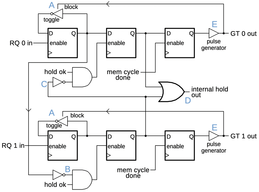
In maximum mode, the top three flip-flops handle the request and grant on line 0, while the bottom three flip-flops handle line 1. At a high level, these flip-flops behave roughly the same as in the minimum mode case, with the first flip-flop tracking the hold request, the second flip-flop activated when the hold is "approved", and the third flip-flop activated when the bus cycle completes. An RQ 0 input will generate a GT 0 output, while a RQ 1 input will generate a GT 1 output. The diagram below is highly simplified, but illustrates the overall behavior. Keep in mind that RQ 0, GT 0, and HOLD use the same physical pin, as do RQ 1, GT 1, and HLDA.

Simplified diagram of the circuitry for maximum mode.

Simplified diagram of the circuitry for maximum mode.

In more detail, the first flip-flop converts the pulse request input into a steady signal. This is accomplished by configuring the first flip-flop is configured with to toggle on when the request pulse is received and toggle off when the end-of-request pulse is received.10 The toggle action is implemented by feeding the output pulse back to the input, inverted (A); since the flip-flop is enabled by the RQ input, the flip-flop holds its value until an input pulse. One tricky part is that the acknowledge pulse must not toggle the flip-flop. This is accomplished by using the output signal to block the toggle. (To keep the diagram simple, I've just noted the "block" action rather than showing the logic.)

As before, the second flip-flop is blocked until the hold is "authorized" to proceed. However, the circuitry is more complicated since it must prioritize the two request lines and ensure that only one hold is granted at a time. If RQ0's first flip-flop is active, it blocks the enable of RQ1's second flip-flop (B). Conversely, if RQ1's second flip-flop is active, it blocks the enable of RQ0's second flip-flop (C). Note the asymmetry, blocking on RQ0's first flip-flop and RQ1's second flip-flop. This enforces the priority of RQ0 over RQ1, since an RQ0 request blocks RQ1 but only an RQ1 "approval" blocks RQ0.

When the second flip-flop is activated in either path, it triggers the internal hold signal (D).8 As before, the hold request is latched into the third flip-flop when any existing memory cycle completes. When the hold request is granted, a pulse is generated (E) on the corresponding GT pin.9

The same circuitry is used for minimum mode and maximum mode, although the above diagrams show differences between the two modes. How does this work? Essentially, logic gates are used to change the behavior between minimum mode and maximum mode as required. For the most part, the circuitry works the same, so only a moderate amount of logic is required to make the same circuitry work for both. On the schematic, the signal MN is active during minimum mode, while MX is active during maximum mode, and these signals control the behavior.

The "hold ok" circuit

As usually happens with the 8086, there are a bunch of special cases when different features interact. One special case is if a bus hold request comes in while the 8086 is acknowledging an interrupt. In this case, the interrupt takes priority and the bus hold is not processed until the interrupt acknowledgment is completed. A second special case is if the bus hold occurs while the 8086 is halted. In this case, the 8086 issues a second HALT indicator at the end of the bus hold. Yet another special case is the 8086's LOCK prefix, which locks the use of the bus for the following instruction, so a bus hold request is not honored until the locked instruction has completed. Finally, the 8086 performs an unaligned word access to memory by breaking it into two 8-bit bus cycles; these two cycles can't be interrupted by a bus hold.

In more detail, the "hold ok" circuit determines at each cycle if a hold could proceed. There are several conditions under which the hold can proceed:

  • The bus cycle is `T2`, except if an unaligned bus operation is taking place (i.e. a word split into two byte operations), or
  • A memory cycle is not active and a microcode memory operation is not taking place, or
  • A memory cycle is not active and a hold is currently active.

The first case occurs during bus (memory) activity, where a hold request before cycle T2 will be handled at the end of that cycle. The second case allows a hold if the bus is inactive. But if microcode is performing a memory operation, the hold will be delayed, even if the request is just starting. The third case is opposite from the other two: it enables the flip flop so a hold request can be dropped. (This ensures that the hold request can still be dropped in the corner case where a hold starts and then the microcode makes a memory request, which will be blocked by the hold.)

The "hold ok" circuit. This has been rearranged from the schematic to make the behavior more clear.

The "hold ok" circuit. This has been rearranged from the schematic to make the behavior more clear.

An instruction with the LOCK prefix causes the bus to be locked against other devices for the duration of the instruction. Thus, a hold cannot be granted while the instruction is running. This is implemented through a separate path. This logic is between the output of the first (request) flip-flop and the second (accepted) flip-flop, tied into the LOCK signal. Conceptually, it seems that the LOCK signal should block hold-ok and thus block the second (accepted) flip-flop from being enabled. But instead, the LOCK signal blocks the data path, unless the request has already been granted. I think the motivation is to allow dropping of a hold request to proceed uninterrupted. In other words, LOCK prevents a hold from being accepted, but it doesn't prevent a hold from being dropped, and it was easier to implement this in the data path.

The pin drive circuitry

The circuitry for the HOLD/RQ0/GT0 and HLDA/RQ1/GT1 pins is somewhat complicated, since they are used for both input and output. In minimum mode, the HOLD pin is an input, while the HLDA pin is an output. In maximum mode, both pins act as an input, with a low-going pulse from an external device to start or stop the hold. But the 8086 also issues pulses to grant the hold. Pull-up resistors inside the 8086 to ensure that the pins remain high (idle) when unused. Finally, an undocumented active pull-up system restores a pin to a high state after it is pulled low, providing faster response than the resistor.

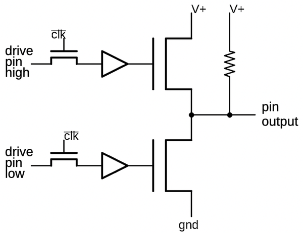
The schematic below shows the heart of the tri-state output circuit. Each pin is connected to two large output MOSFETs, one to drive the pin high and one to drive the pin low. The transistors have separate control lines; if both control lines are low, both transistors are off and the pin floats in the "tri-state" condition. This permits the pin to be used as an input, driven by an external device. The pull-up resistor keeps the pin in a high state.

The tri-state output circuit for each hold pin.

The tri-state output circuit for each hold pin.

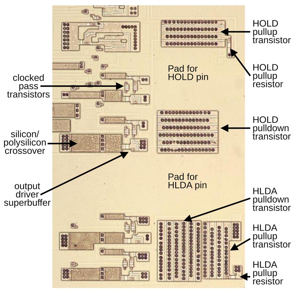
The diagram below shows how this circuitry looks on the die. In this image, the metal and polysilicon layers have been removed with acid to show the underlying doped silicon regions. The thin white stripes are transistor gates where polysilicon wiring crossed the silicon. The black circles are vias that connected the silicon to the metal on top. The empty regions at the right are where the metal pads for HOLD and HLDA were. Next to the pads are the large transistors to pull the outputs high or low. Because the outputs require much higher current than internal signals, these transistors are much larger than logic transistors. They are composed of several transistors placed in parallel, resulting in the parallel stripes. The small pullup resistors are also visible. For efficiency, these resistors are actually depletion-mode transistors, specially doped to act as constant-current sources.

The HOLD/HLDA pin circuitry on the die.

The HOLD/HLDA pin circuitry on the die.

At the left, some of the circuitry is visible. The large output transistors are driven by "superbuffers" that provide more current than regular NMOS buffers. (A superbuffer uses separate transistors to pull the signal high and low, rather than using a pull-up to pull the signal high as in a standard NMOS gate.) The small transistors are the pass transistors that gate output signals according to the clock. The thick rectangles are crossovers, allowing the vertical metal wiring (no longer visible) to cross over a horizontal signal in the signal layer. The 8086 has only a single metal layer, so the layout requires a crossover if signals will otherwise intersect. Because silicon's resistance is much higher than metal's resistance, the crossover is relatively wide to reduce the resistance.

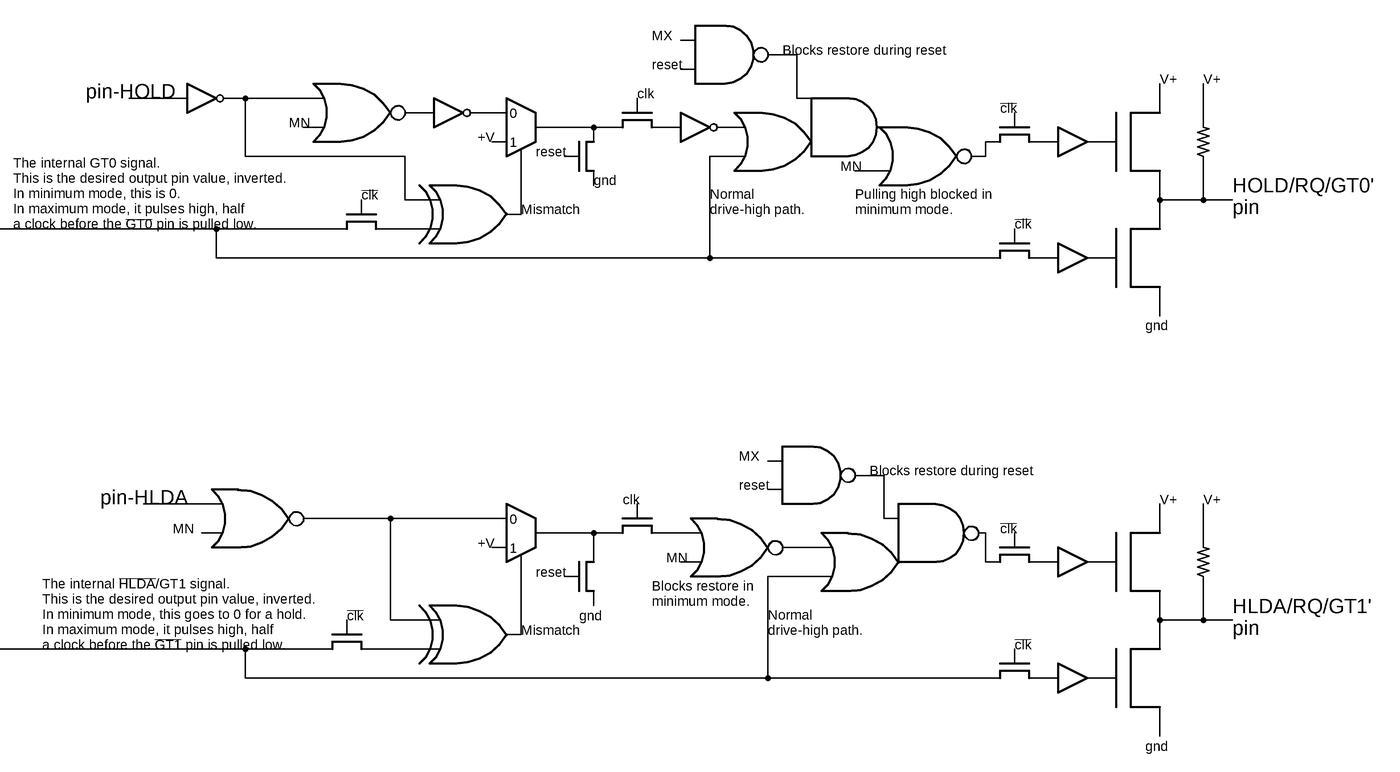
The problem with a pull-up resistor is that it is relatively slow when connected to a line with high capacitance. You essentially end up with a resistor-capacitor delay circuit, as the resistor slowly charges the line and brings it up to a high level. To get around this, the 8086 has an active drive circuit to pulse the RQ/GT lines high to pull them back from a low level. This circuit pulls the line high one cycle after the 8086 drops it low for a grant acknowledge. This circuit also pulls the line high after the external device pulls it low.11 (The schematic for this circuit is in the footnotes.) The curious thing is that I couldn't find this behavior documented in the datasheets. The datasheets describe the internal pull-up resistor, but don't mention that the 8086 actively pulls the lines high.12

Conclusions

The hold circuitry was a key feature of the 8086, largely because it was necessary for the 8087 math coprocessor chip. The hold circuitry seems like it should be straightforward, but there are many corner cases in this circuitry: it interacts with unaligned memory accesses, the LOCK prefix, and minimum vs. maximum modes. As a result, it is fairly complicated.

Personally, I find the hold circuitry somewhat unsatisfying to study, with few fundamental concepts but a lot of special-case logic. The circuitry seems overly complicated for what it does. Much of the complexity is probably due to the wildly different behavior of the pins between minimum and maximum mode. Intel should have simply used a larger package (like the Motorola 68000) rather than re-using pins to support different modes, as well as using the same pin for a request and a grant. It's impressive, however, the same circuitry was made to work for both minimum and maximum modes, despite using completely different signals to request and grant holds. This circuitry must have been a nightmare for Intel's test engineers, trying to ensure that the circuitry performed properly when there were so many corner cases and potential race conditions.

I plan to write more on the 8086, so follow me on Twitter @kenshirriff or RSS for updates. I've also started experimenting with Mastodon recently as @[email protected] and Bluesky as @righto.com so you can follow me there too.

Notes and references

  1. The timing of priority between RQ0 and RQ1 is left vague in the documentation. In practice, even if RQ1 is requested first, a later RQ0 can still preempt it until the point that RQ1 is internally granted (i.e. the second flip-flop is activated). This happens before the hold is externally acknowledged, so it's not obvious to the user at what point priority no longer applies. 

  2. The RQ/GT0 and RQ/GT1 signals are active-low. These signals should have an overbar to indicate this, but it makes the page formatting ugly :-) 

  3. Modern x86 processors still support the 8087 (x87) instruction set. Starting with the 80486DX, the floating point unit was included on the CPU die, rather than as an external coprocessor. The x87 instruction set used a stack-based model, which made it harder to parallelize. To mitigate this, Intel introduced SSE in 1999, a different set of floating point instructions that worked on an independent register set. The x87 instructions are now considered mostly obsolete and are deprecated in 64-bit Windows

  4. The 8087 provides another RQ/GT input line for an external device. Thus, two external devices can still be used in a system with an 8087. That is, although the 8087 uses up one of the 8086's two RQ/GT lines, the 8087 provides another one, so there are still two lines available. The 8087 has logic to combine its bus requests and external bus requests into a single RQ/GT line to the 8086. 

  5. Confusingly, some of the flip-flops in the hold circuit transistion when the clock goes high, while others use the inverted clock signal and transition when the clock goes low. Moreover, the flip-flops are inconsistent about how they treat the data. In each group of three flip-flops, the first flip-flop is active-high, while the remaining flip-flops are active-low. For the most part, I'll ignore this in the discussion. You can look at the schematic if you want to know the details. 

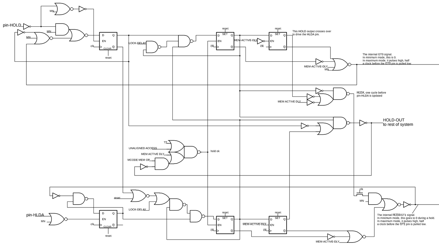
  6. The schematics below shows my reverse-engineered schematic for the hold circuitry. I have partitioned the schematic into the hold logic and the output driver circuitry. This split matches the physical partitioning of the circuitry on the die.

    In the first schematic, the upper part handles HOLD and request0, while the lower part handles request1. There is some circuitry in the middle to handle the common enabling and to generate the internal hold signal. I won't explain the circuitry in much detail, but there are a few things I want to point out. First, even though the hold circuit seems like it should be simple, there are a lot of gates connected in complicated ways. Second, although there are many inverters, NAND, and NOR gates, there are also complex gates such as AND-NOR, OR-NAND, AND-OR-NAND, and so forth. These are implemented as single gates. Due to how gates are constructed from NMOS transistors, it is just as easy to build a hierarchical gate as a single gate. (The last step must be inversion, though.) The XOR gates are more complex; they are constructed from a NOR gate and an AND-NOR gate.

    Schematic of the hold circuitry. Click this image (or any other) for a larger version.

    Schematic of the hold circuitry. Click this image (or any other) for a larger version.

    The schematic below shows the output circuits for the two pins. These circuits are similar, but have a few differences because only the bottom one is used as an output (HLDA) in minimum mode. Each circuit has two inputs: what the current value of the pin is, and what the desired value of the pin is.

    Schematic of the pin output circuits.

    Schematic of the pin output circuits.


  7. Interestingly, the external pins aren't taken out of tri-state mode immediately when the HLDA signal is dropped. Instead, the 8086's bus drivers are re-enabled when a bus cycle starts, which is slightly later. The bus circuitry has a separate flip-flop to manage the enable/disable state, and the start of a bus cycle is what re-enables the bus. This is another example of behavior that the documentation leaves ambiguous. 

  8. There's one more complication for the hold-out signal. If a hold is granted on one line, a request comes in on the other line, and then the hold is released on the first line, the desired behavior is for the bus to remain in the hold state as the hold switches to the second line. However, because of the way a hold on line 1 blocks a hold on line 0, the GT1 second flip-flop will drop a cycle before the GT0 second flip-flop is activated. This would cause hold-out to drop for a cycle and the 8086 could start unwanted bus activity. To prevent this case, the hold-out line is also activated if there is an RQ0 request and RQ1 is granted. This condition seems a bit random but it covers the "gap". I have to wonder if Intel planned the circuit this way, or they added the extra test as a bug fix. (The asymmetry of the priority circuit causes this problem to occur only going from a hold on line 1 to line 0, not the other direction.) 

  9. The pulse-generating circuit is a bit tricky. A pulse signal is generated if the request has been accepted, has not been granted, and will be granted on the next clock (i.e. no memory request is active so the flip-flop is enabled). (Note that the pulse will be one cycle wide, since granting the request on the next cycle will cause the conditions to be no longer satisfied.) This provides the pulse one clock cycle before the flip-flop makes it "official". Moreover, the signals come from the inverted Q outputs from the flip-flops, which are updated half a clock cycle earlier. The result is that the pulse is generated 1.5 clock cycles before the flip-flop output. Presumably the point of this is to respond to hold requests faster, but it seems overly complicated. 

  10. The request pulse is required to be one clock cycle wide. The feedback loop shows why: if the request is longer than one clock cycle, the first flip-flop will repeatedly toggle on and off, resulting in unexpected behavior. 

  11. The details of the active pull-up circuitry don't make sense to me. First it XORs the state of the pin with the desired state of the pin and uses this signal to control a multiplexer, which generates the pull-up action based on other gates. The result of all this ends up being simply NAND, implemented with excessive gates. Another issue is that minimum mode blocks the active pull-up, which makes sense. But there are additional logic gates so minimum mode can affect the value going into the multiplexer, which gets blocked in minimum mode, so that logic seems wasted. There are also two separate circuits to block pull-up during reset. My suspicion is that the original logic accumulated bug fixes and redundant logic wasn't removed. But it's possible that the implementation is doing something clever that I'm just missing. 

  12. My analysis of the RQ/GT lines being pulled high is based on simulation. It would be interesting to verify this behavior on a physical 8086 chip. By measuring the current out of the pin, the pull-up pulses should be visible. 

Undocumented 8086 instructions, explained by the microcode

What happens if you give the Intel 8086 processor an instruction that doesn't exist? A modern microprocessor (80186 and later) will generate an exception, indicating that an illegal instruction was executed. However, early microprocessors didn't include the circuitry to detect illegal instructions, since the chips didn't have transistors to spare. Instead these processors would do something, but the results weren't specified.1

The 8086 has a number of undocumented instructions. Most of them are simply duplicates of regular instructions, but a few have unexpected behavior, such as revealing the values of internal, hidden registers. In the 8086, most instructions are implemented in microcode, so examining the 8086's microcode can explain why these instructions behave the way they do.

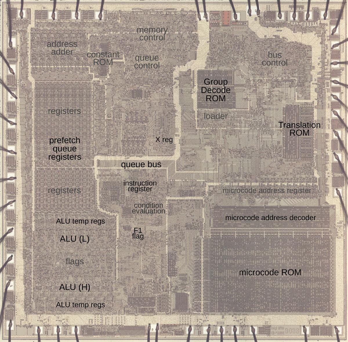
The photo below shows the 8086 die under a microscope, with the important functional blocks labeled. The metal layer is visible, while the underlying silicon and polysilicon wiring is mostly hidden. The microcode ROM and the microcode address decoder are in the lower right. The Group Decode ROM (upper center) is also important, as it performs the first step of instruction decoding.

The 8086 die under a microscope, with main functional blocks labeled. Click on this image (or any other) for a larger version.

The 8086 die under a microscope, with main functional blocks labeled. Click on this image (or any other) for a larger version.

Microcode and 8086 instruction decoding

You might think that machine instructions are the basic steps that a computer performs. However, instructions usually require multiple steps inside the processor. One way of expressing these multiple steps is through microcode, a technique dating back to 1951. To execute a machine instruction, the computer internally executes several simpler micro-instructions, specified by the microcode. In other words, microcode forms another layer between the machine instructions and the hardware. The main advantage of microcode is that it turns the processor's control logic into a programming task instead of a difficult logic design task.

The 8086's microcode ROM holds 512 micro-instructions, each 21 bits wide. Each micro-instruction performs two actions in parallel. First is a move between a source and a destination, typically registers. Second is an operation that can range from an arithmetic (ALU) operation to a memory access. The diagram below shows the structure of a 21-bit micro-instruction, divided into six types.

The encoding of a micro-instruction into 21 bits. Based on NEC v. Intel: Will Hardware Be Drawn into the Black Hole of Copyright?

The encoding of a micro-instruction into 21 bits. Based on NEC v. Intel: Will Hardware Be Drawn into the Black Hole of Copyright?

When executing a machine instruction, the 8086 performs a decoding step. Although the 8086 is a 16-bit processor, its instructions are based on bytes. In most cases, the first byte specifies the opcode, which may be followed by additional instruction bytes. In other cases, the byte is a "prefix" byte, which changes the behavior of the following instruction. The first byte is analyzed by something called the Group Decode ROM. This circuit categorizes the first byte of the instruction into about 35 categories that control how the instruction is decoded and executed. One category is "1-byte logic"; this indicates a one-byte instruction or prefix that is simple and implemented by logic circuitry in the 8086. For instructions in this category, microcode is not involved while the remaining instructions are implemented in microcode. Many of these instructions are in the "two-byte ROM" category indicating that the instruction has a second byte that also needs to be decoded by microcode. This second byte, called the ModR/M byte, specifies that memory addressing mode or registers that the instruction uses.

The next step is the microcode's address decoder circuit, which determines where to start executing microcode based on the opcode. Conceptually, you can think of the microcode as stored in a ROM, indexed by the instruction opcode and a few sequence bits. However, since many instructions can use the same microcode, it would be inefficient to store duplicate copies of these routines. Instead, the microcode address decoder permits multiple instructions to reference the same entries in the ROM. This decoding circuitry is similar to a PLA (Programmable Logic Array) so it matches bit patterns to determine a particular starting point. This turns out to be important for undocumented instructions since undocumented instructions often match the pattern for a "real" instruction, making the undocumented instruction an alias.

The 8086 has several internal registers that are invisible to the programmer but are used by the microcode. Memory accesses use the Indirect (IND) and Operand (OPR) registers; the IND register holds the address in the segment, while the OPR register holds the data value that is read or written. Although these registers are normally not accessible by the programmer, some undocumented instructions provide access to these registers, as will be described later.

The Arithmetic/Logic Unit (ALU) performs arithmetic, logical, and shift operations in the 8086. The ALU uses three internal registers: tmpA, tmpB, and tmpC. An ALU operation requires two micro-instructions. The first micro-instruction specifies the operation (such as ADD) and the temporary register that holds one argument (e.g. tmpA); the second argument is always in tmpB. A following micro-instruction can access the ALU result through the pseudo-register Σ (sigma).

The ModR/M byte

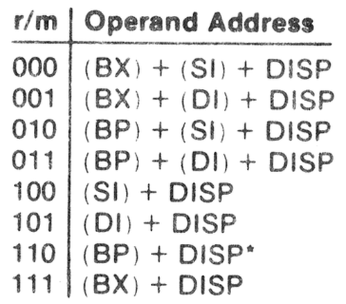
A fundamental part of the 8086 instruction format is the ModR/M byte, a byte that specifies addressing for many instructions. The 8086 has a variety of addressing modes, so the ModR/M byte is somewhat complicated. Normally it specifies one memory address and one register. The memory address is specified through one of eight addressing modes (below) along with an optional 8- or 16-bit displacement in the instruction. Instead of a memory address, the ModR/M byte can also specify a second register. For a few opcodes, the ModR/M byte selects what instruction to execute rather than a register.

The 8086's addressing modes. From The register assignments, from MCS-86 Assembly Language Reference Guide.

The implementation of the ModR/M byte plays an important role in the behavior of undocumented instructions. Support for this byte is implemented in both microcode and hardware. The various memory address modes above are implemented by microcode subroutines, which compute the appropriate memory address and perform a read if necessary. The subroutine leaves the memory address in the IND register, and if a read is performed, the value is in the OPR register.

The hardware hides the ModR/M byte's selection of memory versus register, by making the value available through the pseudo-register M, while the second register is available through N. Thus, the microcode for an instruction doesn't need to know if the value was in memory or a register, or which register was selected. The Group Decode ROM examines the first byte of the instruction to determine if a ModR/M byte is present, and if a read is required. If the ModR/M byte specifies memory, the Translation ROM determines which micro-subroutines to call before handling the instruction itself. For more on the ModR/M byte, see my post on Reverse-engineering the ModR/M addressing microcode.

Holes in the opcode table

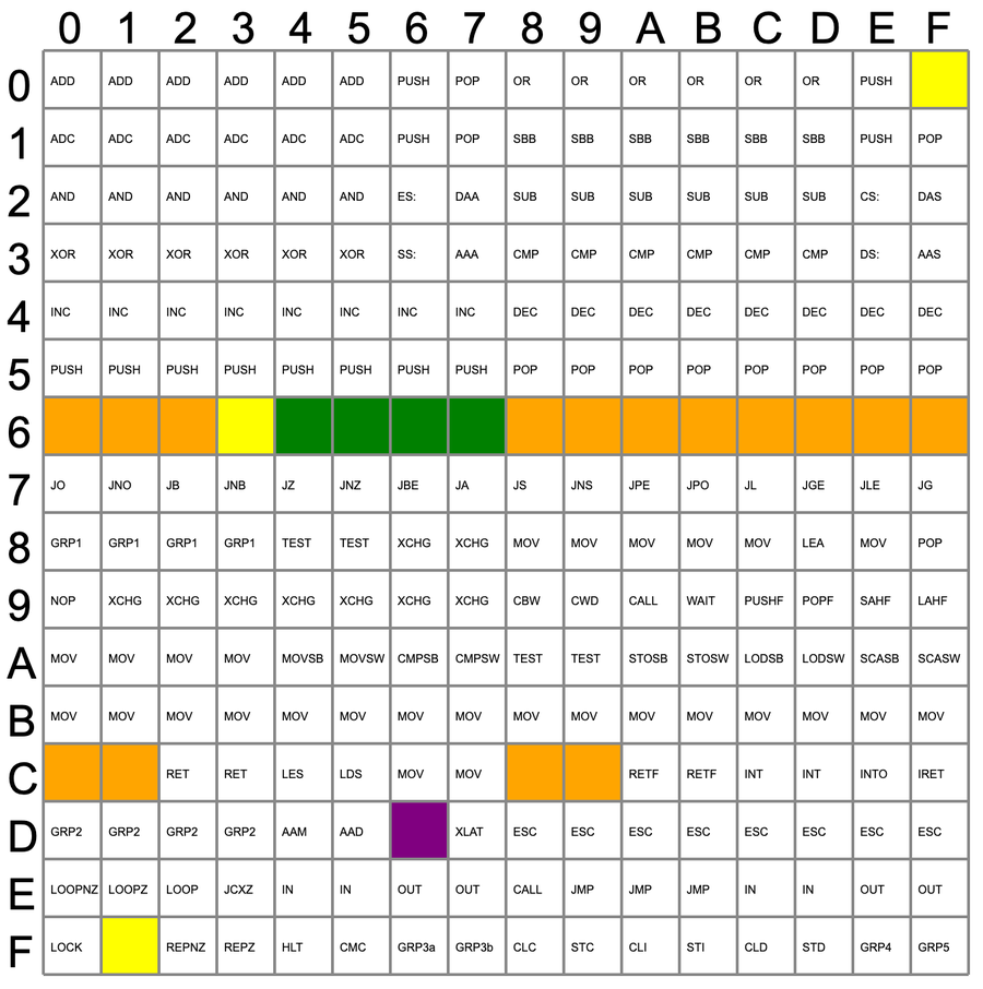
The first byte of the instruction is a value from 00 to FF in hex. Almost all of these opcode values correspond to documented 8086 instructions, but there are a few exceptions, "holes" in the opcode table. The table below shows the 256 first-byte opcodes for the 8086, from hex 00 to FF. Valid opcodes for the 8086 are in white; the colored opcodes are undefined and interesting to examine. Orange, yellow, and green opcodes were given meaning in the 80186, 80286, and 80386 respectively. The purple opcode is unusual: it was implemented in the 8086 and later processors but not documented.2 In this section, I'll examine the microcode for these opcode holes.

This table shows the 256 opcodes for the 8086, where the white ones are valid instructions. Click for a larger version.

This table shows the 256 opcodes for the 8086, where the white ones are valid instructions. Click for a larger version.

D6: SALC

The opcode D6 (purple above) performs a well-known but undocumented operation that is typically called SALC, for Set AL to Carry. This instruction sets the AL register to 0 if the carry flag is 0, and sets the AL register to FF if the carry flag is 1. The curious thing about this undocumented instruction is that it exists in all x86 CPUs, but Intel didn't mention it until 2017. Intel probably put this instruction into the processor deliberately as a copyright trap. The idea is that if a company created a copy of the 8086 processor and the processor included the SALC instruction, this would prove that the company had copied Intel's microcode and thus had potentially violated Intel's copyright on the microcode. This came to light when NEC created improved versions of the 8086, the NEC V20 and V30 microprocessors, and was sued by Intel. Intel analyzed NEC's microcode but was disappointed to find that NEC's chip did not include the hidden instruction, showing that NEC hadn't copied the microcode.3 Although a Federal judge ruled in 1989 that NEC hadn't infringed Intel's copyright, the 5-year trial ruined NEC's market momentum.

The SALC instruction is implemented with three micro-instructions, shown below.4 The first micro-instruction jumps if the carry (CY) is set. If not, the next instruction moves 0 to the AL register. RNI (Run Next Instruction) ends the microcode execution causing the next machine instruction to run. If the carry was set, all-ones (i.e. FF hex) is moved to the AL register and RNI ends the microcode sequence.

           JMPS CY 2 SALC: jump on carry
ZERO → AL  RNI       Move 0 to AL, run next instruction
ONES → AL  RNI       2:Move FF to AL, run next instruction

0F: POP CS

The 0F opcode is the first hole in the opcode table. The 8086 has instructions to push and pop the four segment registers, except opcode 0F is undefined where POP CS should be. This opcode performs POP CS successfully, so the question is why is it undefined? The reason is that POP CS is essentially useless and doesn't do what you'd expect, so Intel figured it was best not to document it.

To understand why POP CS is useless, I need to step back and explain the 8086's segment registers. The 8086 has a 20-bit address space, but 16-bit registers. To make this work, the 8086 has the concept of segments: memory is accessed in 64K chunks called segments, which are positioned in the 1-megabyte address space. Specifically, there are four segments: Code Segment, Stack Segment, Data Segment, and Extra Segment, with four segment registers that define the start of the segment: CS, SS, DS, and ES.

An inconvenient part of segment addressing is that if you want to access more than 64K, you need to change the segment register. So you might push the data segment register, change it temporarily so you can access a new part of memory, and then pop the old data segment register value off the stack. This would use the PUSH DS and POP DS instructions. But why not POP CS?

The 8086 executes code from the code segment, with the instruction pointer (IP) tracking the location in the code segment. The main problem with POP CS is that it changes the code segment, but not the instruction pointer, so now you are executing code at the old offset in a new segment. Unless you line up your code extremely carefully, the result is that you're jumping to an unexpected place in memory. (Normally, you want to change CS and the instruction pointer at the same time, using a CALL or JMP instruction.)

The second problem with POP CS is prefetching. For efficiency, the 8086 prefetches instructions before they are needed, storing them in an 6-byte prefetch queue. When you perform a jump, for instance, the microcode flushes the prefetch queue so execution will continue with the new instructions, rather than the old instructions. However, the instructions that pop a segment register don't flush the prefetch buffer. Thus, POP CS not only jumps to an unexpected location in memory, but it will execute an unpredictable number of instructions from the old code path.

The POP segment register microcode below packs a lot into three micro-instructions. The first micro-instruction pops a value from the stack. Specifically, it moves the stack pointer (SP) to the Indirect (IND) register. The Indirect register is an internal register, invisible to the programmer, that holds the address offset for memory accesses. The first micro-instruction also performs a memory read (R) from the stack segment (SS) and then increments IND by 2 (P2, plus 2). The second micro-instruction moves IND to the stack pointer, updating the stack pointer with the new value. It also tells the microcode engine that this micro-instruction is the next-to-last (NXT) and the next machine instruction can be started. The final micro-instruction moves the value read from memory to the appropriate segment register and runs the next instruction. Specifically, reads and writes put data in the internal OPR (Operand) register. The hardware uses the register N to indicate the register specified by the instruction. That is, the value will be stored in the CS, DS, ES, or SS register, depending on the bit pattern in the instruction. Thus, the same microcode works for all four segment registers. This is why POP CS works even though POP CS wasn't explicitly implemented in the microcode; it uses the common code.

SP → IND  R SS,P2 POP sr: read from stack, compute IND plus 2
IND → SP  NXT     Put updated value in SP, start next instruction.
OPR → N   RNI     Put stack value in specified segment register

But why does POP CS run this microcode in the first place? The microcode to execute is selected based on the instruction, but multiple instructions can execute the same microcode. You can think of the address decoder as pattern-matching on the instruction's bit patterns, where some of the bits can be ignored. In this case, the POP sr microcode above is run by any instruction with the bit pattern 000??111, where a question mark can be either a 0 or a 1. You can verify that this pattern matches POP ES (07), POP SS (17), and POP DS (1F). However, it also matches 0F, which is why the 0F opcode runs the above microcode and performs POP CS. In other words, to make 0F do something other than POP CS would require additional circuitry, so it was easier to leave the action implemented but undocumented.

60-6F: conditional jumps

One whole row of the opcode table is unused: values 60 to 6F. These opcodes simply act the same as 70 to 7F, the conditional jump instructions.

The conditional jumps use the following microcode. It fetches the jump offset from the instruction prefetch queue (Q) and puts the value into the ALU's tmpBL register, the low byte of the tmpB register. It tests the condition in the instruction (XC) and jumps to the RELJMP micro-subroutine if satisfied. The RELJMP code (not shown) updates the program counter to perform the jump.

Q → tmpBL                Jcond cb: Get offset from prefetch queue
           JMP XC RELJMP Test condition, if true jump to RELJMP routine
           RNI           No jump: run next instruction

This code is executed for any instruction matching the bit pattern 011?????, i.e. anything from 60 to 7F. The condition is specified by the four low bits of the instruction. The result is that any instruction 60-6F is an alias for the corresponding conditional jump 70-7F.

C0, C8: RET/RETF imm

These undocumented opcodes act like a return instruction, specifically RET imm16 (source). Specifically, the instruction C0 is the same as C2, near return, while C8 is the same as CA, far return.

The microcode below is executed for the instruction bits 1100?0?0, so it is executed for C0, C2, C8, and CA. It gets two bytes from the instruction prefetch queue (Q) and puts them in the tmpA register. Next, it calls FARRET, which performs either a near return (popping PC from the stack) or a far return (popping PC and CS from the stack). Finally, it adds the original argument to the SP, equivalent to popping that many bytes.

Q → tmpAL    ADD tmpA    RET/RETF iw: Get word from prefetch, set up ADD
Q → tmpAH    CALL FARRET Call Far Return micro-subroutine
IND → tmpB               Move SP (in IND) to tmpB for ADD
Σ → SP       RNI         Put sum in Stack Pointer, end

One tricky part is that the FARRET micro-subroutine examines bit 3 of the instruction to determine whether it does a near return or a far return. This is why documented instruction C2 is a near return and CA is a far return. Since C0 and C8 run the same microcode, they will perform the same actions, a near return and a far return respectively.

C1: RET

The undocumented C1 opcode is identical to the documented C3, near return instruction. The microcode below is executed for instruction bits 110000?1, i.e. C1 and C3. The first micro-instruction reads from the Stack Pointer, incrementing IND by 2. Prefetching is suspended and the prefetch queue is flushed, since execution will continue at a new location. The Program Counter is updated with the value from the stack, read into the OPR register. Finally, the updated address is put in the Stack Pointer and execution ends.

SP → IND  R SS,P2  RET:  Read from stack, increment by 2
          SUSP     Suspend prefetching
OPR → PC  FLUSH    Update PC from stack, flush prefetch queue
IND → SP  RNI      Update SP, run next instruction

C9: RET

The undocumented C9 opcode is identical to the documented CB, far return instruction. This microcode is executed for instruction bits 110010?1, i.e. C9 and CB, so C9 is identical to CB. The microcode below simply calls the FARRET micro-subroutine to pop the Program Counter and CS register. Then the new value is stored into the Stack Pointer. One subtlety is that FARRET looks at bit 3 of the instruction to switch between a near return and a far return, as described earlier. Since C9 and CB both have bit 3 set, they both perform a far return.

          CALL FARRET  RETF: call FARRET routine
IND → SP  RNI          Update stack pointer, run next instruction

F1: LOCK prefix

The final hole in the opcode table is F1. This opcode is different because it is implemented in logic rather than microcode. The Group Decode ROM indicates that F1 is a prefix, one-byte logic, and LOCK. The Group Decode outputs are the same as F0, so F1 also acts as a LOCK prefix.

Holes in two-byte opcodes

For most of the 8086 instructions, the first byte specifies the instruction. However, the 8086 has a few instructions where the second byte specifies the instruction: the reg field of the ModR/M byte provides an opcode extension that selects the instruction.5 These fall into four categories which Intel labeled "Immed", "Shift", "Group 1", and "Group 2", corresponding to opcodes 80-83, D0-D3, F6-F7, and FE-FF. The table below shows how the second byte selects the instruction. Note that "Shift", "Group 1", and "Group 2" all have gaps, resulting in undocumented values.

Meaning of the reg field in two-byte opcodes. From MCS-86 Assembly Language Reference Guide.

Meaning of the reg field in two-byte opcodes. From MCS-86 Assembly Language Reference Guide.

These sets of instructions are implemented in two completely different ways. The "Immed" and "Shift" instructions run microcode in the standard way, selected by the first byte. For a typical arithmetic/logic instruction such as ADD, bits 5-3 of the first instruction byte are latched into the X register to indicate which ALU operation to perform. The microcode specifies a generic ALU operation, while the X register controls whether the operation is an ADD, SUB, XOR, or so forth. However, the Group Decode ROM indicates that for the special "Immed" and "Shift" instructions, the X register latches the bits from the second byte. Thus, when the microcode executes a generic ALU operation, it ends up with the one specified in the second byte.6

The "Group 1" and "Group 2" instructions (F0-F1, FE-FF), however, run different microcode for each instruction. Bits 5-3 of the second byte replace bits 2-0 of the instruction before executing the microcode. Thus, F0 and F1 act as if they are opcodes in the range F0-F7, while FE and FF act as if they are opcodes in the range F8-FF. Thus, each instruction specified by the second byte can have its own microcode, unlike the "Immed" and "Shift" instructions. The trick that makes this work is that all the "real" opcodes in the range F0-FF are implemented in logic, not microcode, so there are no collisions.

The hole in "Shift": SETMO, D0..D3/6

There is a "hole" in the list of shift operations when the second byte has the bits 110 (6). (This is typically expressed as D0/6 and so forth; the value after the slash is the opcode-selection bits in the ModR/M byte.) Internally, this value selects the ALU's SETMO (Set Minus One) operation, which simply returns FF or FFFF, for a byte or word operation respectively.7

The microcode below is executed for 1101000? bit patterns patterns (D0 and D1). The first instruction gets the value from the M register and sets up the ALU to do whatever operation was specified in the instruction (indicated by XI). Thus, the same microcode is used for all the "Shift" instructions, including SETMO. The result is written back to M. If no writeback to memory is required (NWB), then RNI runs the next instruction, ending the microcode sequence. However, if the result is going to memory, then the last line writes the value to memory.

M → tmpB  XI tmpB, NXT  rot rm, 1: get argument, set up ALU
Σ → M     NWB,RNI F     Store result, maybe run next instruction
          W DS,P0 RNI   Write result to memory

The D2 and D3 instructions (1101001?) perform a variable number of shifts, specified by the CL register, so they use different microcode (below). This microcode loops the number of times specified by CL, but the control flow is a bit tricky to avoid shifting if the intial counter value is 0. The code sets up the ALU to pass the counter (in tmpA) unmodified the first time (PASS) and jumps to 4, which updates the counter and sets up the ALU for the shift operation (XI). If the counter is not zero, it jumps back to 3, which performs the previously-specified shift and sets up the ALU to decrement the counter (DEC). This time, the code at 4 decrements the counter. The loop continues until the counter reaches zero. The microcode stores the result as in the previous microcode.

ZERO → tmpA               rot rm,CL: 0 to tmpA
CX → tmpAL   PASS tmpA    Get count to tmpAL, set up ALU to pass through
M → tmpB     JMPS 4       Get value, jump to loop (4)
Σ → tmpB     DEC tmpA F   3: Update result, set up decrement of count
Σ → tmpA     XI tmpB      4: update count in tmpA, set up ALU
             JMPS NZ 3    Loop if count not zero
tmpB → M     NWB,RNI      Store result, maybe run next instruction
             W DS,P0 RNI  Write result to memory

The hole in "group 1": TEST, F6/1 and F7/1

The F6 and F7 opcodes are in "group 1", with the specific instruction specified by bits 5-3 of the second byte. The second-byte table showed a hole for the 001 bit sequence. As explained earlier, these bits replace the low-order bits of the instruction, so F6 with 001 is processed as if it were the opcode F1. The microcode below matches against instruction bits 1111000?, so F6/1 and F7/1 have the same effect as F6/0 and F7/1 respectively, that is, the byte and word TEST instructions.

The microcode below gets one or two bytes from the prefetch queue (Q); the L8 condition tests if the operation is an 8-bit (i.e. byte) operation and skips the second micro-instruction. The third micro-instruction ANDs the argument and the fetched value. The condition flags (F) are set based on the result, but the result itself is discarded. Thus, the TEST instruction tests a value against a mask, seeing if any bits are set.

Q → tmpBL    JMPS L8 2     TEST rm,i: Get byte, jump if operation length = 8
Q → tmpBH                  Get second byte from the prefetch queue
M → tmpA     AND tmpA, NXT 2: Get argument, AND with fetched value
Σ → no dest  RNI F         Discard result but set flags.

I explained the processing of these "Group 3" instructions in more detail in my microcode article.

The hole in "group 2": PUSH, FE/7 and FF/7

The FE and FF opcodes are in "group 2", which has a hole for the 111 bit sequence in the second byte. After replacement, this will be processed as the FF opcode, which matches the pattern 1111111?. In other words, the instruction will be processed the same as the 110 bit pattern, which is PUSH. The microcode gets the Stack Pointer, sets up the ALU to decrement it by 2. The new value is written to SP and IND. Finally, the register value is written to stack memory.

SP → tmpA  DEC2 tmpA   PUSH rm: set up decrement SP by 2
Σ → IND                Decremented SP to IND
Σ → SP                 Decremented SP to SP
M → OPR    W SS,P0 RNI Write the value to memory, done

82 and 83 "Immed" group

Opcodes 80-83 are the "Immed" group, performing one of eight arithmetic operations, specified in the ModR/M byte. The four opcodes differ in the size of the values: opcode 80 applies an 8-bit immediate value to an 8-bit register, 81 applies a 16-bit value to a 16-bit register, 82 applies an 8-bit value to an 8-bit register, and 83 applies an 8-bit value to a 16-bit register. The opcode 82 has the strange situation that some sources say it is undocumented, but it shows up in some Intel documentation as a valid bit combination (e.g. below). Note that 80 and 82 have the 8-bit to 8-bit action, so the 82 opcode is redundant.

ADC is one of the instructions with opcode 80-83. From the 8086 datasheet, page 27.

ADC is one of the instructions with opcode 80-83. From the 8086 datasheet, page 27.

The microcode below is used for all four opcodes. If the ModR/M byte specifies memory, the appropriate micro-subroutine is called to compute the effective address in IND, and fetch the byte or word into OPR. The first two instructions below get the two immediate data bytes from the prefetch queue; for an 8-bit operation, the second byte is skipped. Next, the second argument M is loaded into tmpA and the desired ALU operation (XI) is configured. The result Σ is stored into the specified register M and the operation may terminate with RNI. But if the ModR/M byte specified memory, the following write micro-operation saves the value to memory.

Q → tmpBL  JMPS L8 2    alu rm,i: get byte, test if 8-bit op
Q → tmpBH               Maybe get second byte
M → tmpA   XI tmpA, NXT 2: 
Σ → M      NWB,RNI F    Save result, update flags, done if no memory writeback
           W DS,P0 RNI  Write result to memory if needed

The tricky part of this is the L8 condition, which tests if the operation is 8-bit. You might think that bit 0 acts as the byte/word bit in a nice, orthogonal way, but the 8086 has a bunch of special cases. Bit 0 of the instruction typically selects between a byte and a word operation, but there are a bunch of special cases. The Group Decode ROM creates a signal indicating if bit 0 should be used as the byte/word bit. But it generates a second signal indicating that an instruction should be forced to operate on bytes, for instructions such as DAA and XLAT. Another Group Decode ROM signal indicates that bit 3 of the instruction should select byte or word; this is used for the MOV instructions with opcodes Bx. Yet another Group Decode ROM signal indicates that inverted bit 1 of the instruction should select byte or word; this is used for a few opcodes, including 80-87.

The important thing here is that for the opcodes under discussion (80-83), the L8 micro-condition uses both bits 0 and 1 to determine if the instruction is 8 bits or not. The result is that only opcode 81 is considered 16-bit by the L8 test, so it is the only one that uses two immediate bytes from the instruction. However, the register operations use only bit 0 to select a byte or word transfer. The result is that opcode 83 has the unusual behavior of using an 8-bit immediate operand with a 16-bit register. In this case, the 8-bit value is sign-extended to form a 16-bit value. That is, the top bit of the 8-bit value fills the entire upper half of the 16-bit value, converting an 8-bit signed value to a 16-bit signed value (e.g. -1 is FF, which becomes FFFF). This makes sense for arithmetic operations, but not much sense for logical operations.

Intel documentation is inconsistent about which opcodes are listed for which instructions. Intel opcode maps generally define opcodes 80-83. However, lists of specific instructions show opcodes 80, 81, and 83 for arithmetic operations but only 80 and 81 for logical operations.8 That is, Intel omits the redundant 82 opcode as well as omitting logic operations that perform sign-extension (83).

More FE holes

For the "group 2" instructions, the FE opcode performs a byte operation while FF performs a word operation. Many of these operations don't make sense for bytes: CALL, JMP, and PUSH. (The only instructions supported for FE are INC and DEC.) But what happens if you use the unsupported instructions? The remainder of this section examines those cases and shows that the results are not useful.

CALL: FE/2

This instruction performs an indirect subroutine call within a segment, reading the target address from the memory location specified by the ModR/M byte.

The microcode below is a bit convoluted because the code falls through into the shared NEARCALL routine, so there is some unnecessary register movement. Before this microcode executes, the appropriate ModR/M micro-subroutine will read the target address from memory. The code below copies the destination address from M to tmpB and stores it into the PC later in the code to transfer execution. The code suspends prefetching, corrects the PC to cancel the offset from prefetching, and flushes the prefetch queue. Finally, it decrements the SP by two and writes the old PC to the stack.

M → tmpB    SUSP        CALL rm: read value, suspend prefetch
SP → IND    CORR        Get SP, correct PC
PC → OPR    DEC2 tmpC   Get PC to write, set up decrement
tmpB → PC   FLUSH       NEARCALL: Update PC, flush prefetch
IND → tmpC              Get SP to decrement
Σ → IND                 Decremented SP to IND
Σ → SP      W SS,P0 RNI Update SP, write old PC to stack

This code will mess up in two ways when executed as a byte instruction. First, when the destination address is read from memory, only a byte will be read, so the destination address will be corrupted. (I think that the behavior here depends on the bus hardware. The 8086 will ask for a byte from memory but will read the word that is placed on the bus. Thus, if memory returns a word, this part may operate correctly. The 8088's behavior will be different because of its 8-bit bus.) The second issue is writing the old PC to the stack because only a byte of the PC will be written. Thus, when the code returns from the subroutine call, the return address will be corrupt.

CALL: FE/3

This instruction performs an indirect subroutine call between segments, reading the target address from the memory location specified by the ModR/M byte.

IND → tmpC  INC2 tmpC    CALL FAR rm: set up IND+2
Σ → IND     R DS,P0      Read new CS, update IND
OPR → tmpA  DEC2 tmpC    New CS to tmpA, set up SP-2
SP → tmpC   SUSP         FARCALL: Suspend prefetch
Σ → IND     CORR         FARCALL2: Update IND, correct PC
CS → OPR    W SS,M2      Push old CS, decrement IND by 2
tmpA → CS   PASS tmpC    Update CS, set up for NEARCALL
PC → OPR    JMP NEARCALL Continue with NEARCALL

As in the previous CALL, this microcode will fail in multiple ways when executed in byte mode. The new CS and PC addresses will be read from memory as bytes, which may or may not work. Only a byte of the old CS and PC will be pushed to the stack.

JMP: FE/4

This instruction performs an indirect jump within a segment, reading the target address from the memory location specified by the ModR/M byte. The microcode is short, since the ModR/M micro-subroutine does most of the work. I believe this will have the same problem as the previous CALL instructions, that it will attempt to read a byte from memory instead of a word.

        SUSP       JMP rm: Suspend prefetch
M → PC  FLUSH RNI  Update PC with new address, flush prefetch, done

JMP: FE/5

This instruction performs an indirect jump between segments, reading the new PC and CS values from the memory location specified by the ModR/M byte. The ModR/M micro-subroutine reads the new PC address. This microcode increments IND and suspends prefetching. It updates the PC, reads the new CS value from memory, and updates the CS. As before, the reads from memory will read bytes instead of words, so this code will not meaningfully work in byte mode.

IND → tmpC  INC2 tmpC   JMP FAR rm: set up IND+2
Σ → IND     SUSP        Update IND, suspend prefetch
tmpB → PC   R DS,P0     Update PC, read new CS from memory
OPR → CS    FLUSH RNI   Update CS, flush prefetch, done

PUSH: FE/6

This instruction pushes the register or memory value specified by the ModR/M byte. It decrements the SP by 2 and then writes the value to the stack. It will write one byte to the stack but decrements the SP by 2, so one byte of old stack data will be on the stack along with the data byte.

SP → tmpA  DEC2 tmpA    PUSH rm: Set up SP decrement 
Σ → IND                 Decremented value to IND
Σ → SP                  Decremented value to SP
M → OPR    W SS,P0 RNI  Write the data to the stack

Undocumented instruction values

The next category of undocumented instructions is where the first byte indicates a valid instruction, but there is something wrong with the second byte.

AAM: ASCII Adjust after Multiply

The AAM instruction is a fairly obscure one, designed to support binary-coded decimal arithmetic (BCD). After multiplying two BCD digits, you end up with a binary value between 0 and 81 (0×0 to 9×9). If you want a BCD result, the AAM instruction converts this binary value to BCD, for instance splitting 81 into the decimal digits 8 and 1, where the upper digit is 81 divided by 10, and the lower digit is 81 modulo 10.

The interesting thing about AAM is that the 2-byte instruction is D4 0A. You might notice that hex 0A is 10, and this is not a coincidence. There wasn't an easy way to get the value 10 in the microcode, so instead they made the instruction provide that value in the second byte. The undocumented (but well-known) part is that if you provide a value other than 10, the instruction will convert the binary input into digits in that base. For example, if you provide 8 as the second byte, the instruction returns the value divided by 8 and the value modulo 8.

The microcode for AAM, below, sets up the registers. calls the CORD (Core Division) micro-subroutine to perform the division, and then puts the results into AH and AL. In more detail, the CORD routine divides tmpA/tmpC by tmpB, putting the complement of the quotient in tmpC and leaving the remainder in tmpA. (If you want to know how CORD works internally, see my division post.) The important step is that the AAM microcode gets the divisor from the prefetch queue (Q). After calling CORD, it sets up the ALU to perform a 1's complement of tmpC and puts the result (Σ) into AH. It sets up the ALU to pass tmpA through unchanged, puts the result (Σ) into AL, and updates the flags accordingly (F).

Q → tmpB                    AAM: Move byte from prefetch to tmpB
ZERO → tmpA                 Move 0 to tmpA
AL → tmpC    CALL CORD      Move AL to tmpC, call CORD.
             COM1 tmpC      Set ALU to complement
Σ → AH       PASS tmpA, NXT Complement AL to AH
Σ → AL       RNI F          Pass tmpA through ALU to set flags

The interesting thing is why this code has undocumented behavior. The 8086's microcode only has support for the constants 0 and all-1's (FF or FFFF), but the microcode needs to divide by 10. One solution would be to implement an additional micro-instruction and more circuitry to provide the constant 10, but every transistor was precious back then. Instead, the designers took the approach of simply putting the number 10 as the second byte of the instruction and loading the constant from there. Since the AAM instruction is not used very much, making the instruction two bytes long wasn't much of a drawback. But if you put a different number in the second byte, that's the divisor the microcode will use. (Of course you could add circuitry to verify that the number is 10, but then the implementation is no longer simple.)

Intel could have documented the full behavior, but that creates several problems. First, Intel would be stuck supporting the full behavior into the future. Second, there are corner cases to deal with, such as divide-by-zero. Third, testing the chip would become harder because all these cases would need to be tested. Fourth, the documentation would become long and confusing. It's not surprising that Intel left the full behavior undocumented.

AAD: ASCII Adjust before Division

The AAD instruction is analogous to AAM but used for BCD division. In this case, you want to divide a two-digit BCD number by something, where the BCD digits are in AH and AL. The AAD instruction converts the two-digit BCD number to binary by computing AH×10+AL, before you perform the division.

The microcode for AAD is shown below. The microcode sets up the registers, calls the multiplication micro-subroutine CORX (Core Times), and then puts the results in AH and AL. In more detail, the multiplier comes from the instruction prefetch queue Q. The CORX routine multiples tmpC by tmpB, putting the result in tmpA/tmpC. Then the microcode adds the low BCD digit (AL) to the product (tmpB + tmpC), putting the sum (Σ) into AL, clearing AH and setting the status flags F appropriately.

One interesting thing is that the second-last micro-instruction jumps to AAEND, which is the last micro-instruction of the AAM microcode above. By reusing the micro-instruction from AAM, the microcode is one micro-instruction shorter, but the jump adds one cycle to the execution time. (The CORX routine is used for integer multiplication; I discuss the internals in this post.)

Q → tmpC              AAD: Get byte from prefetch queue.
AH → tmpB   CALL CORX Call CORX
AL → tmpB   ADD tmpC  Set ALU for ADD
ZERO → AH   JMP AAEND Zero AH, jump to AAEND
i
...
Σ → AL      RNI F     AAEND: Sum to AL, done.

As with AAM, the constant 10 is provided in the second byte of the instruction. The microcode accepts any value here, but values other than 10 are undocumented.

8C, 8E: MOV sr

The opcodes 8C and 8E perform a MOV register to or from the specified segment register, using the register specification field in the ModR/M byte. There are four segment registers and three selection bits, so an invalid segment register can be specified. However, the hardware that decodes the register number ignores instruction bit 5 for a segment register. Thus, specifying a segment register 4 to 7 is the same as specifying a segment register 0 to 3. For more details, see my article on 8086 register codes.

Unexpected REP prefix

REP IMUL / IDIV

The REP prefix is used with string operations to cause the operation to be repeated across a block of memory. However, if you use this prefix with an IMUL or IDIV instruction, it has the unexpected behavior of negating the product or the quotient (source).

The reason for this behavior is that the string operations use an internal flag called F1 to indicate that a REP prefix has been applied. The multiply and divide code reuses this flag to track the sign of the input values, toggling F1 for each negative value. If F1 is set, the value at the end is negated. (This handles "two negatives make a positive.") The consequence is that the REP prefix puts the flag in the 1 state when the multiply/divide starts, so the computed sign will be wrong at the end and the result is the negative of the expected result. The microcode is fairly complex, so I won't show it here; I explain it in detail in this blog post.

REP RET

Wikipedia lists REP RET (i.e. RET with a REP prefix) as a way to implement a two-byte return instruction. This is kind of trivial; the RET microcode (like almost every instruction) doesn't use the F1 internal flag, so the REP prefix has no effect.

REPNZ MOVS/STOS

Wikipedia mentions that the use of the REPNZ prefix (as opposed to REPZ) is undefined with string operations other than CMPS/SCAS. An internal flag called F1Z distinguishes between the REPZ and REPNZ prefixes. This flag is only used by CMPS/SCAS. Since the other string instructions ignore this flag, they will ignore the difference between REPZ and REPNZ. I wrote about string operations in more detail in this post.

Using a register instead of memory.

Some instructions are documented as requiring a memory operand. However, the ModR/M byte can specify a register. The behavior in these cases can be highly unusual, providing access to hidden registers. Examining the microcode shows how this happens.

LEA reg

Many instructions have a ModR/M byte that indicates the memory address that the instruction should use, perhaps through a complicated addressing mode. The LEA (Load Effective Address) instruction is different: it doesn't access the memory location but returns the address itself. The undocumented part is that the ModR/M byte can specify a register instead of a memory location. In that case, what does the LEA instruction do? Obviously it can't return the address of a register, but it needs to return something.

The behavior of LEA is explained by how the 8086 handles the ModR/M byte. Before running the microcode corresponding to the instruction, the microcode engine calls a short micro-subroutine for the particular addressing mode. This micro-subroutine puts the desired memory address (the effective address) into the tmpA register. The effective address is copied to the IND (Indirect) register and the value is loaded from memory if needed. On the other hand, if the ModR/M byte specified a register instead of memory, no micro-subroutine is called. (I explain ModR/M handling in more detail in this article.)

The microcode for LEA itself is just one line. It stores the effective address in the IND register into the specified destination register, indicated by N. This assumes that the appropriate ModR/M micro-subroutine was called before this code, putting the effective address into IND.

IND → N   RNI  LEA: store IND register in destination, done

But if a register was specified instead of a memory location, no ModR/M micro-subroutine gets called. Instead, the LEA instruction will return whatever value was left in IND from before, typically the previous memory location that was accessed. Thus, LEA can be used to read the value of the IND register, which is normally hidden from the programmer.

LDS reg, LES reg

The LDS and LES instructions load a far pointer from memory into the specified segment register and general-purpose register. The microcode below assumes that the appropriate ModR/M micro-subroutine has set up IND and read the first value into OPR. The microcode updates the destination register, increments IND by 2, reads the next value, and updates DS. (The microcode for LES is a copy of this, but updates ES.)

OPR → N               LDS: Copy OPR to dest register
IND → tmpC  INC2 tmpC Set up incrementing IND by 2
Σ → IND     R DS,P0   Update IND, read next location
OPR → DS    RNI       Update DS

If the LDS instruction specifies a register instead of memory, a micro-subroutine will not be called, so IND and OPR will have values from a previous instruction. OPR will be stored in the destination register, while the DS value will be read from the address IND+2. Thus, these instructions provide a mechanism to access the hidden OPR register.

JMP FAR rm

The JMP FAR rm instruction normally jumps to the far address stored in memory at the location indicated by the ModR/M byte. (That is, the ModR/M byte indicates where the new PC and CS values are stored.) But, as with LEA, the behavior is undocumented if the ModR/M byte specifies a register, since a register doesn't hold a four-byte value.

The microcode explains what happens. As with LEA, the code expects a micro-subroutine to put the address into the IND register. In this case, the micro-subroutine also loads the value at that address (i.e. the destination PC) into tmpB. The microcode increments IND by 2 to point to the CS word in memory and reads that into CS. Meanwhile, it updates the PC with tmpB. It suspends prefetching and flushes the queue, so instruction fetching will restart at the new address.

IND → tmpC  INC2 tmpC   JMP FAR rm: set up to add 2 to IND
Σ → IND     SUSP        Update IND, suspend prefetching
tmpB → PC   R DS,P0     Update PC with tmpB. Read new CS from specified address
OPR → CS    FLUSH RNI   Update CS, flush queue, done

If you specify a register instead of memory, the micro-subroutine won't get called. Instead, the program counter will be loaded with whatever value was in tmpB and the CS segment register will be loaded from the memory location two bytes after the location that IND was referencing. Thus, this undocumented use of the instruction gives access to the otherwise-hidden tmpB register.

The end of undocumented instructions

Microprocessor manufacturers soon realized that undocumented instructions were a problem, since programmers find them and often use them. This creates an issue for future processors, or even revisions of the current processor: if you eliminate an undocumented instruction, previously-working code that used the instruction will break, and it will seem like the new processor is faulty.

The solution was for processors to detect undocumented instructions and prevent them from executing. By the early 1980s, processors had enough transistors (thanks to Moore's law) that they could include the circuitry to block unsupported instructions. In particular, the 80186/80188 and the 80286 generated a trap of type 6 when an unused opcode was executed, blocking use of the instruction.9 This trap is also known as #UD (Undefined instruction trap).10

Conclusions

The 8086, like many early microprocessors, has undocumented instructions but no traps to stop them from executing.11 For the 8086, these fall into several categories. Many undocumented instructions simply mirror existing instructions. Some instructions are implemented but not documented for one reason or another, such as SALC and POP CS. Other instructions can be used outside their normal range, such as AAM and AAD. Some instructions are intended to work only with a memory address, so specifying a register can have strange effects such as revealing the values of the hidden IND and OPR registers.

Keep in mind that my analysis is based on transistor-level simulation and examining the microcode; I haven't verified the behavior on a physical 8086 processor. Please let me know if you see any errors in my analysis or undocumented instructions that I have overlooked. Also note that the behavior could change between different versions of the 8086; in particular, some versions by different manufacturers (such as the NEC V20 and V30) are known to be different.

I plan to write more about the 8086, so follow me on Twitter @kenshirriff or RSS for updates. I've also started experimenting with Mastodon recently as @[email protected] and Bluesky as @righto.com so you can follow me there too.

Notes and references

  1. The 6502 processor, for instance, has illegal instructions with various effects, including causing the processor to hang. The article How MOS 6502 illegal opcodes really work describes in detail how the instruction decoding results in various illegal opcodes. Some of these opcodes put the internal bus into a floating state, so the behavior is electrically unpredictable. 

  2. The 8086 used up almost all the single-byte opcodes, which made it difficult to extend the instruction set. Most of the new instructions for the 386 or later are multi-byte opcodes, either using 0F as a prefix or reusing the earlier REP prefix (F3). Thus, the x86 instruction set is less efficient than it could be, since many single-byte opcodes were "wasted" on hardly-used instructions such as BCD arithmetic, forcing newer instructions to be multi-byte. 

  3. For details on the "magic instruction" hidden in the 8086 microcode, see NEC v. Intel: Will Hardware Be Drawn into the Black Hole of Copyright Editors page 49. I haven't found anything stating that SALC was the hidden instruction, but this is the only undocumented instruction that makes sense as something deliberately put into the microcode. The court case is complicated since NEC had a licensing agreement with Intel, so I'm skipping lots of details. See NEC v. Intel: Breaking new ground in the law of copyright for more. 

  4. The microcode listings are based on Andrew Jenner's disassembly. I have made some modifications to (hopefully) make it easier to understand. 

  5. Specifying the instruction through the ModR/M reg field may seem a bit random, but there's a reason for this. A typical instruction such as ADD has two arguments specified by the ModR/M byte. But other instructions such as shift instructions or NOT only take one argument. For these instructions, the ModR/M reg field would be wasted if it specified a register. Thus, using the reg field to specify instructions that only use one argument makes the instruction set more efficient. 

  6. Note that "normal" ALU operations are specified by bits 5-3 of the instruction; in order these are ADD, OR, ADC, SBB, AND, SUB, XOR, and CMP. These are exactly the same ALU operations that the "Immed" group performs, specified by bits 5-3 of the second byte. This illustrates how the same operation selection mechanism (the X register) is used in both cases. Bit 6 of the instruction switches between the set of arithmetic/logic instructions and the set of shift/rotate instructions. 

  7. As far as I can tell, SETMO isn't used by the microcode. Thus, I think that SETMO wasn't deliberately implemented in the ALU, but is a consequence of how the ALU's control logic is implemented. That is, all the even entries are left shifts and the odd entries are right shifts, so operation 6 activates the left-shift circuitry. But it doesn't match a specific left shift operation, so the ALU doesn't get configured for a "real" left shift. In other words, the behavior of this instruction is due to how the ALU handles a case that it wasn't specifically designed to handle.

    This function is implemented in the ALU somewhat similar to a shift left. However, instead of passing each input bit to the left, the bit from the right is passed to the left. That is, the input to bit 0 is shifted left to all of the bits of the result. By setting this bit to 1, all bits of the result are set, yielding the minus 1 result. 

  8. This footnote provides some references for the "Immed" opcodes. The 8086 datasheet has an opcode map showing opcodes 80 through 83 as valid. However, in the listings of individual instructions it only shows 80 and 81 for logical instructions (i.e. bit 1 must be 0), while it shows 80-83 for arithmetic instructions. The modern Intel 64 and IA-32 Architectures Software Developer's Manual is also contradictory. Looking at the instruction reference for AND (Vol 2A 3-78), for instance, shows opcodes 80, 81, and 83, explicitly labeling 83 as sign-extended. But the opcode map (Table A-2 Vol 2D A-7) shows 80-83 as defined except for 82 in 64-bit mode. The instruction bit diagram (Table B-13 Vol 2D B-7) shows 80-83 valid for the arithmetic and logical instructions. 

  9. The 80286 was more thorough about detecting undefined opcodes than the 80186, even taking into account the differences in instruction set. The 80186 generates a trap when 0F, 63-67, F1, or FFFF is executed. The 80286 generates invalid opcode exception number 6 (#UD) on any undefined opcode, handling the following cases:

    • The first byte of an instruction is completely invalid (e.g., 64H).
    • The first byte indicates a 2-byte opcode and the second byte is invalid (e.g., 0F followed by 0FFH).
    • An invalid register is used with an otherwise valid opcode (e.g., MOV CS,AX).
    • An invalid opcode extension is given in the REG field of the ModR/M byte (e.g., 0F6H /1).
    • A register operand is given in an instruction that requires a memory operand (e.g., LGDT AX).
     

  10. In modern x86 processors, most undocumented instructions cause faults. However, there are still a few undocumented instructions that don't fault. These may be for internal use or corner cases of documented instructions. For details, see Breaking the x86 Instruction Set, a video from Black Hat 2017. 

  11. Several sources have discussed undocumented 8086 opcodes before. The article Undocumented 8086 Opcodes describes undocumented opcodes in detail. Wikipedia has a list of undocumented x86 instructions. The book Undocumented PC discusses undocumented instructions in the 8086 and later processors. This StackExchange Retrocomputing post describes undocumented instructions. These Hacker News comments discuss some undocumented instructions. There are other sources with more myth than fact, claiming that the 8086 treats undocumented instructions as NOPs, for instance.