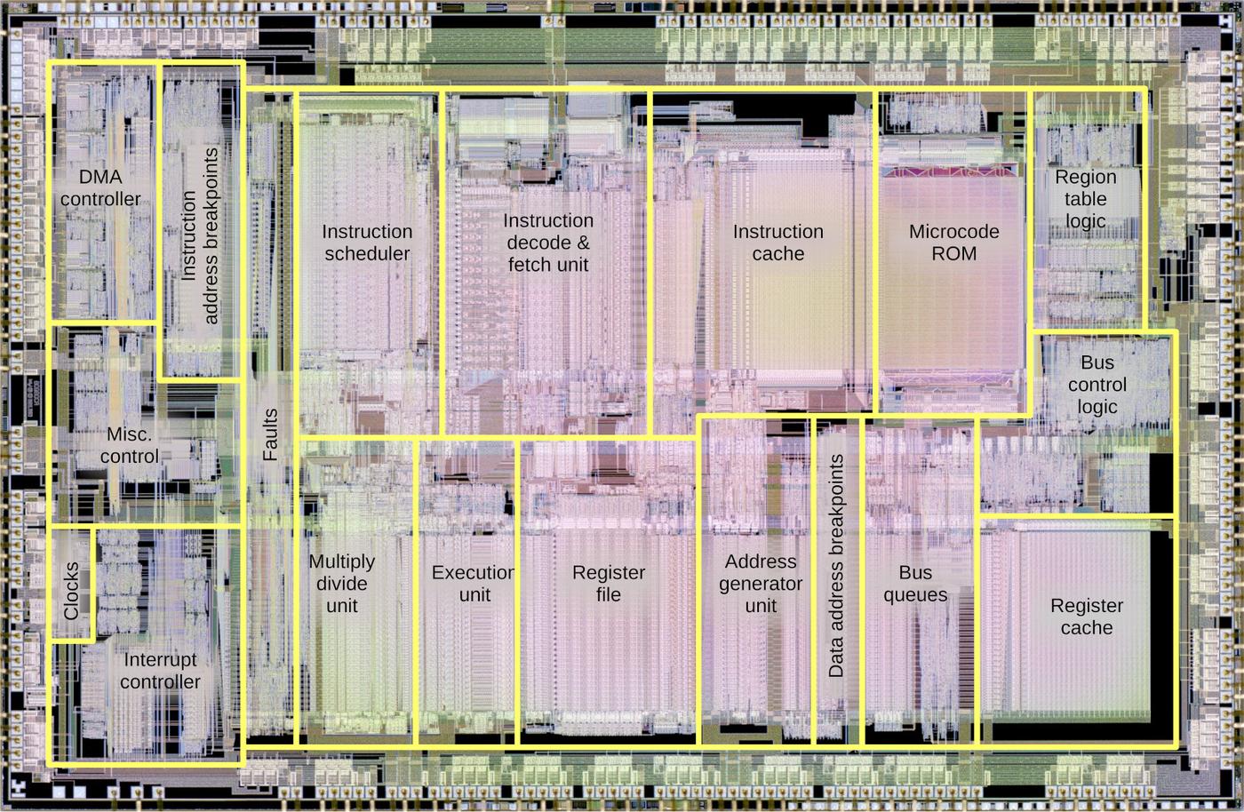
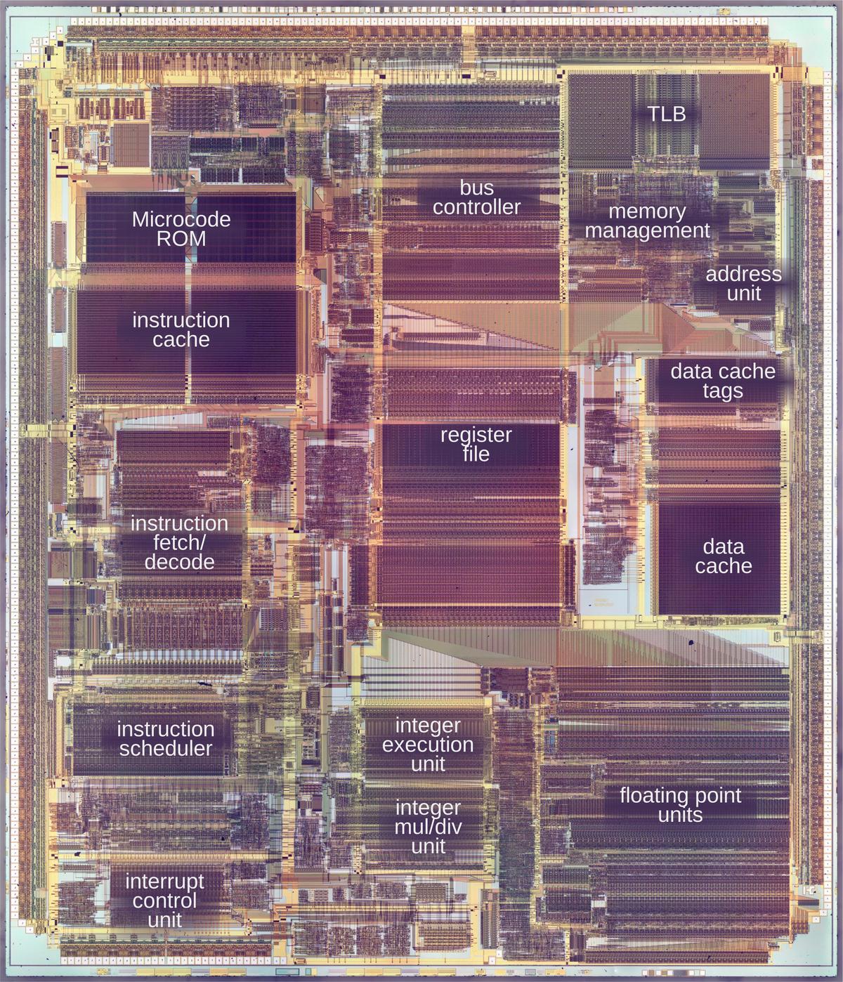
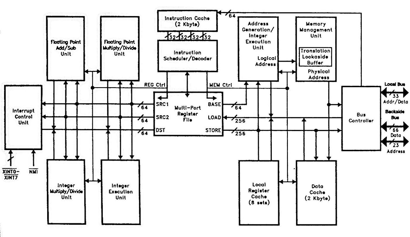
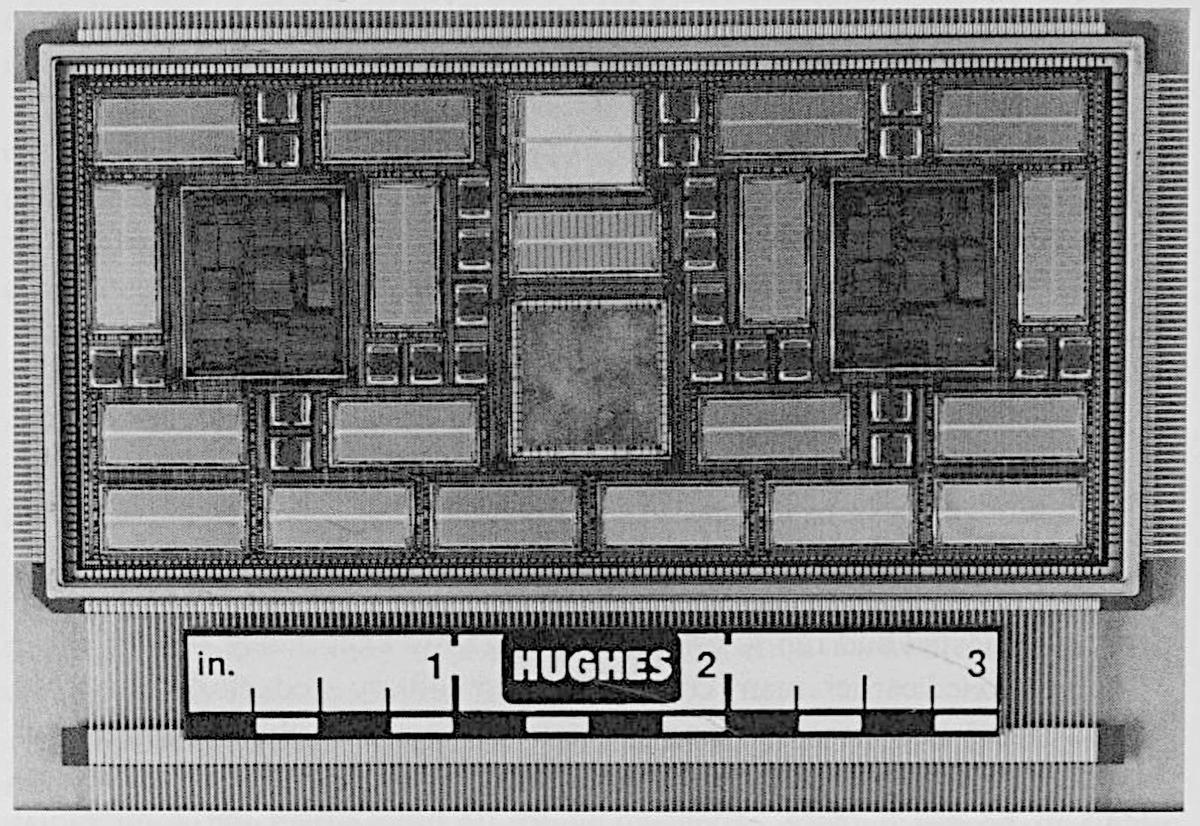
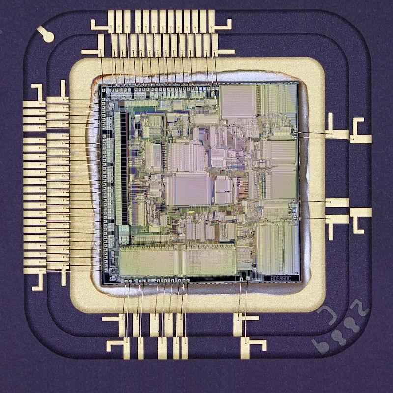
The Intel 8086 microprocessor (1978) started the x86 architecture that continues to this day. In this blog post, I'm focusing on a small part of the chip: the address and data pins that connect the chip to external memory and I/O devices. In many processors, this circuitry is straightforward, but it is complicated in the 8086 for two reasons. First, Intel decided to package the 8086 as a 40-pin DIP, which didn't provide enough pins for all the functionality. Instead, the 8086 multiplexes address, data, and status. In other words, a pin can have multiple roles, providing an address bit at one time and a data bit at another time.
The second complication is that the 8086 has a 20-bit address space (due to its infamous segment registers), while the data bus is 16 bits wide. As will be seen, the "extra" four address bits have more impact than you might expect. To summarize, 16 pins, called AD0-AD15, provide 16 bits of address and data. The four remaining address pins (A16-A19) are multiplexed for use as status pins, providing information about what the processor is doing for use by other parts of the system. You might expect that the 8086 would thus have two types of pin circuits, but it turns out that there are four distinct circuits, which I will discuss below.
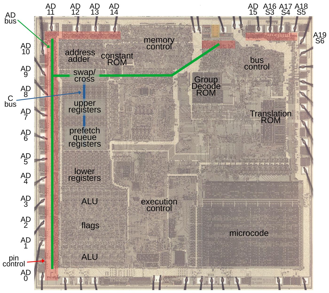
The microscope image above shows the silicon die of the 8086. In this image, the metal layer on top of the chip is visible, while the silicon and polysilicon underneath are obscured. The square pads around the edge of the die are connected by tiny bond wires to the chip's 40 external pins. The 20 address pins are labeled: Pins AD0 through AD15 function as address and data pins. Pins A16 through A19 function as address pins and status pins.1 The circuitry that controls the pins is highlighted in red. Two internal busses are important for this discussion: the 20-bit AD bus (green) connects the AD pins to the rest of the CPU, while the 16-bit C bus (blue) communicates with the registers. These buses are connected through a circuit that can swap the byte order or shift the value. (The lines on the diagram are simplified; the real wiring twists and turns to fit the layout. Moreover, the C bus (blue) has its bits spread across the width of the register file.)
Segment addressing in the 8086
One goal of the 8086 design was to maintain backward compatibility with the earlier 8080 processor.2 This had a major impact on the 8086's memory design, resulting in the much-hated segment registers. The 8080 (like most of the 8-bit processors of the early 1970s) had a 16-bit address space, able to access 64K (65,536 bytes) of memory, which was plenty at the time. But due to the exponential growth in memory capacity described by Moore's Law, it was clear that the 8086 needed to support much more. Intel decided on a 1-megabyte address space, requiring 20 address bits. But Intel wanted to keep the 16-bit memory addresses used by the 8080.
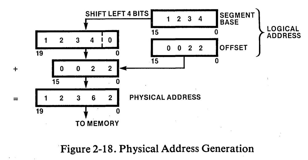
The solution was to break memory into segments. Each segment was 64K long, so a 16-bit offset was sufficient to access memory in a segment. The segments were allocated in a 1-megabyte address space, with the result that you could access a megabyte of memory, but only in 64K chunks.3 Segment addresses were also 16 bits, but were shifted left by 4 bits (multiplied by 16) to support the 20-bit address space.
Thus, every memory access in the 8086 required a computation of the physical address. The diagram below illustrates this process: the logical address consists of the segment base address and the offset within the segment. The 16-bit segment register was shifted 4 bits and added to the 16-bit offset to yield the 20-bit physical memory address.
This address computation was not performed by the regular ALU (Arithmetic/Logic Unit), but by a separate adder that was devoted to address computation. The address adder is visible in the upper-left corner of the die photo. I will discuss the address adder in more detail below.
The AD bus and the C Bus
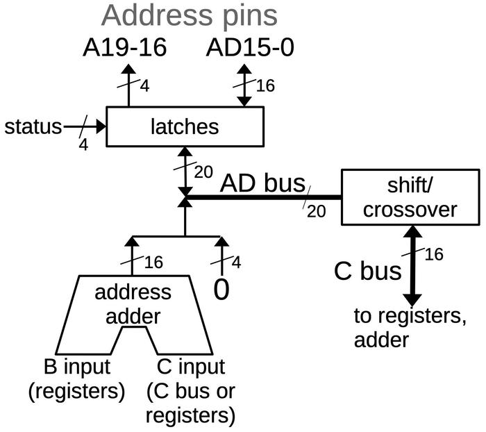
The 8086 has multiple internal buses to move bits internally, but the relevant ones are the AD bus and the C bus. The AD bus is a 20-bit bus that connects the 20 address/data pins to the internal circuitry.4 A 16-bit bus called the C bus provides the connection between the AD bus, the address adder and some of the registers.5 The diagram below shows the connections. The AD bus can be connected to the 20 address pins through latches. The low 16 pins can also be used for data input, while the upper 4 pins can also be used for status output. The address adder performs the 16-bit addition necessary for segment arithmetic. Its output is shifted left by four bits (i.e. it has four 0 bits appended), producing the 20-bit result. The inputs to the adder are provided by registers, a constant ROM that holds small constants such as +1 or -2, or the C bus.
The shift/crossover circuit provides the interface between these two buses, handling the 20-bit to 16-bit conversion. The busses can be connected in three ways: direct, crossover, or shifted.6 The direct mode connects the 16 bits of the C bus to the lower 16 bits of the address/data pins. This is the standard mode for transferring data between the 8086's internal circuitry and the data pins. The crossover mode performs the same connection but swaps the bytes. This is typically used for unaligned memory accesses, where the low memory byte corresponds to the high register byte, or vice versa. The shifted mode shifts the 20-bit AD bus value four positions to the right. In this mode, the 16-bit output from the address adder goes to the 16-bit C bus. (The shift is necessary to counteract the 4-bit shift applied to the address adder's output.) Control circuitry selects the right operation for the shift/crossover circuit at the right time.7
Two of the registers are invisible to the programmer but play an important role in memory accesses.
The IND (Indirect) register specifies the memory address; it holds the 16-bit memory offset in a segment.
The OPR (Operand) register holds the data value.9
The IND and OPR registers are not accessed directly by the programmer; the microcode for a machine instruction moves the appropriate
values to these registers prior to the write.
Overview of a write cycle
I hesitate to present a timing diagram, since I may scare off my readers, but the 8086's communication is designed around a four-step bus cycle. The diagram below shows simplified timing for a write cycle, when the 8086 writes to memory or an I/O device.8 The external bus activity is organized as four states, each one clock cycle long: T1, T2, T3, T4. These T states are very important since they control what happens on the bus. During T1, the 8086 outputs the address on the pins. During the T2, T3, and T4 states, the 8086 outputs the data word on the pins. The important part for this discussion is that the pins are multiplexed depending on the T-state: the pins provide the address during T1 and data during T2 through T4.
There two undocumented T states that are important to the bus cycle. The physical address is computed in the two clock cycles before T1 so the address will be available in T1. I give these "invisible" T states the names TS (start) and T0.
The address adder
The operation of the address adder is a bit tricky since the 16-bit adder must generate a 20-bit physical address. The adder has two 16-bit inputs: the B input is connected to the upper registers via the B bus, while the C input is connected to the C bus. The segment register value is transferred over the B bus to the adder during the second half of the TS state (that is, two clock cycles before the bus cycle becomes externally visible during T1). Meanwhile, the address offset is transferred over the C bus to the adder, but the adder's C input shifts the value four bits to the right, discarding the four low bits. (As will be explained later, the pin driver circuits latch these bits.) The adder's output is shifted left four bits and transferred to the AD bus during the second half of T0. This produces the upper 16 bits of the 20-bit physical memory address. This value is latched into the address output flip-flops at the start of T1, putting the computed address on the pins. To summarize, the 20-bit address is generated by storing the 4 low-order bits during T0 and then the 16 high-order sum bits during T1.
The address adder is not needed for segment arithmetic during T1 and T2.
To improve performance, the 8086 uses the adder during this idle time to increment or decrement memory addresses.
For instance, after popping a word from the stack, the stack pointer needs to be incremented by 2.
The address adder can do this increment "for free" during T1 and T2, leaving the ALU available for other operations.10
Specifically, the adder updates the memory address in IND, incrementing it or decrementing it as appropriate.
First, the IND value is transferred over the B bus to the adder during the second half of T1.
Meanwhile, a constant (-3 to +2) is loaded from the Constant ROM and transferred to the adder's C input.
The output from the adder is transferred to the AD bus during the second half of T2.
As before, the output is shifted four bits to the left. However, the shift/crossover circuit between the AD bus and the C bus
is configured to shift four bits to the right, canceling the adder's shift.
The result is that the C bus gets the 16-bit sum from the adder, and this value is stored in the IND register.11
For more information on the implemenation of the address adder, see my previous blog post.
The pin driver circuit
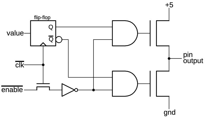
Now I'll dive down to the hardware implementation of an output pin. When the 8086 chip communicates with the outside world, it needs to provide relatively high currents. The tiny logic transistors can't provide enough current, so the chip needs to use large output transistors. To fit the large output transistors on the die, they are constructed of multiple wide transistors in parallel.12 Moreover, the drivers use a somewhat unusual "superbuffer" circuit with two transistors: one to pull the output high, and one to pull the output low.13
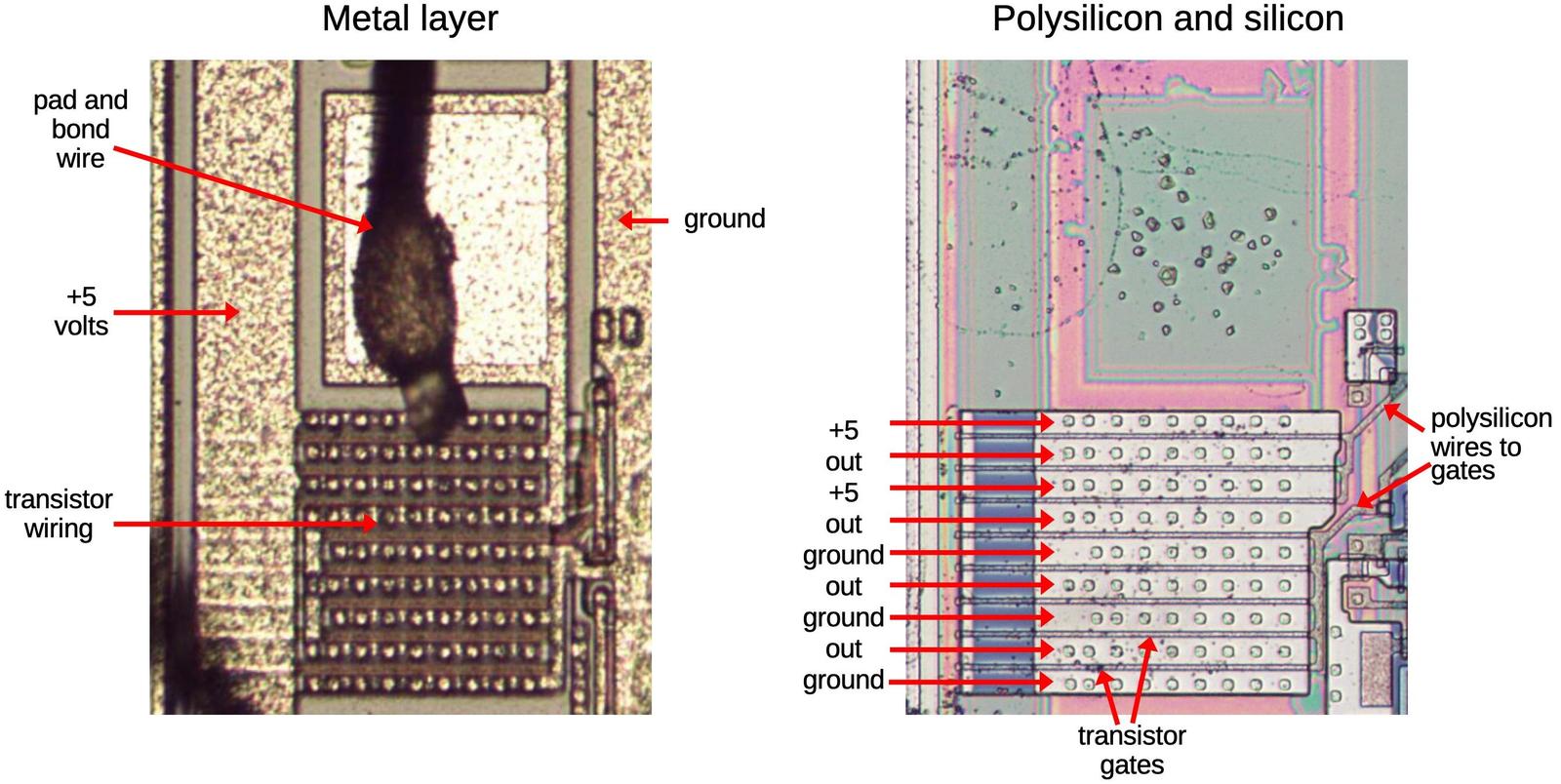
The diagram below shows the transistor structure for one of the output pins (AD10), consisting of three parallel transistors between the output and +5V, and five parallel transistors between the output and ground. The die photo on the left shows the metal layer on top of the die. This shows the power and ground wiring and the connections to the transistors. The photo on the right shows the die with the metal layer removed, showing the underlying silicon and the polysilicon wiring on top. A transistor gate is formed where a polysilicon wire crosses the doped silicon region. Combined, the +5V transistors are equivalent to about 60 typical transistors, while the ground transistors are equivalent to about 100 typical transistors. Thus, these transistors provide substantially more current to the output pin.
Tri-state output driver
The output circuit for an address pin uses a tri-state buffer, which allows the output to be disabled by putting it into a high-impedance "tri-state" configuration. In this state, the output is not pulled high or low but is left floating. This capability allows the pin to be used for data input. It also allows external devices to device can take control of the bus, for instance, to perform DMA (direct memory access).
The pin is driven by two large MOSFETs, one to pull the output high and one to pull it low. (As described earlier, each large MOSFET is physically multiple transistors in parallel, but I'll ignore that for now.) If both MOSFETs are off, the output floats, neither on nor off.
The tri-state output is implemented by driving the MOSFETs with two "superbuffer"15 AND gates.
If the enable input is low, both AND gates produce a low output and both output transistors are off.
On the other hand, if enable is high, one AND gate will be on and one will be off.
The desired output value is loaded into a flip-flop to hold it,14
and the flip-flop turns one of the output transistors on, driving the output pin high or low as appropriate.
(Conveniently, the flip-flop provides the data output Q and the inverted data output Q.)
Generally, the address pin outputs are enabled for T1-T4 of a write but only during T1 for a read.16
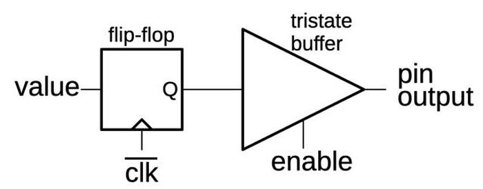
In the remainder of the discussion, I'll use the tri-state buffer symbol below, rather than showing the implementation of the buffer.
AD4-AD15
Pins AD4-AD15 are "typical" pins, avoiding the special behavior of the top and bottom pins, so I'll discuss them first.
The behavior of these pins is that the value on the AD bus is latched by the circuit and then put on the output pin
under the control of the enaable signal.
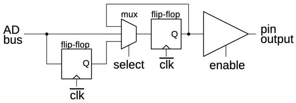
The circuit has three parts: a multiplexer to select the output value, a flip-flop to hold the output value, and a tri-state driver to
provide the high-current output to the pin.
In more detail, the multiplexer selects either the value on the AD bus or the current output from the flip-flop.
That is, the multiplexer can either load a new value into the flip-flop or hold the existing value.17
The flip-flop latches the input value on the falling edge of the clock, passing it to the output driver.
If the enable line is high, the output driver puts this value on the corresponding address pin.
For a write, the circuit latches the address value on the bus during the second half of T0 and puts it on the pins during T1.
During the second half of the T1 state, the data word is transferred from the OPR register over the C bus to the AD bus and loaded
into the AD pin latches.
The word is transferred from the latches to the pins during T2 and held for the remainder of the bus cycle.
AD0-AD3
The four low address bits have a more complex circuit because these address bits are latched from the bus before the address adder computes its sum, as described earlier. The memory offset (before the segment addition) will be on the C bus during the second half of TS and is loaded into the lower flip-flop. This flip-flop delays these bits for one clock cycle and then they are loaded into the upper flip-flop. Thus, these four pins pick up the offset prior to the addition, while the other pins get the result of the segment addition.
For data, the AD0-AD3 pins transfer data directly from the AD bus to the pin latch, bypassing the delay that was used to get the address bits. That is, the AD0-AD3 pins have two paths: the delayed path used for addresses during T0 and the direct path otherwise used for data. Thus, the multiplexer has three inputs: two for these two paths and a third loop-back input to hold the flip-flop value.
A16-A19: status outputs
The top four pins (A16-A19) are treated specially, since they are not used for data. Instead, they provide processor status during T2-T4.18 The pin latches for these pins are loaded with the address during T0 like the other pins, but loaded with status instead of data during T1. The multiplexer at the input to the latch selects the address bit during T0 and the status bit during T1, and holds the value otherwise. The schematic below shows how this is implemented for A16, A17, and A19.
Address pin A18 is different because it indicates the current status of the interrupt enable flag bit. This status is updated every clock cycle, unlike the other pins. To implement this, the pin has a different circuit that isn't latched, so the status can be updated continuously. The clocked transistors act as "pass transistors", passing the signal through when active. When a pass transistor is turned off, the following logic gate holds the previous value due to the capacitance of the wiring. Thus, the pass transistors provide a way of holding the value through the clock cycle. The flip-flops are implemented with pass transistors internally, so in a sense the circuit below is a flip-flop that has been "exploded" to provide a second path for the interrupt status.
Reads
A memory or I/O read also uses a 4-state bus cycle, slightly different from the write cycle.
During T1, the address is provided on the pins, the same as for a write.
After that, however, the output circuits are tri-stated so they float, allowing the external memory to put data on the bus.
The read data on the pin is put on the AD bus at the start of the T4 state.
From there, the data passes through the crossover circuit to the C bus. Normally the 16 data bits pass straight through to
the C bus, but the bytes will be swapped if the memory access is unaligned.
From the C bus, the data is written to the OPR register, a byte or a word as appropriate.
(For an instruction prefetch, the word is written to a prefetch queue register instead.)
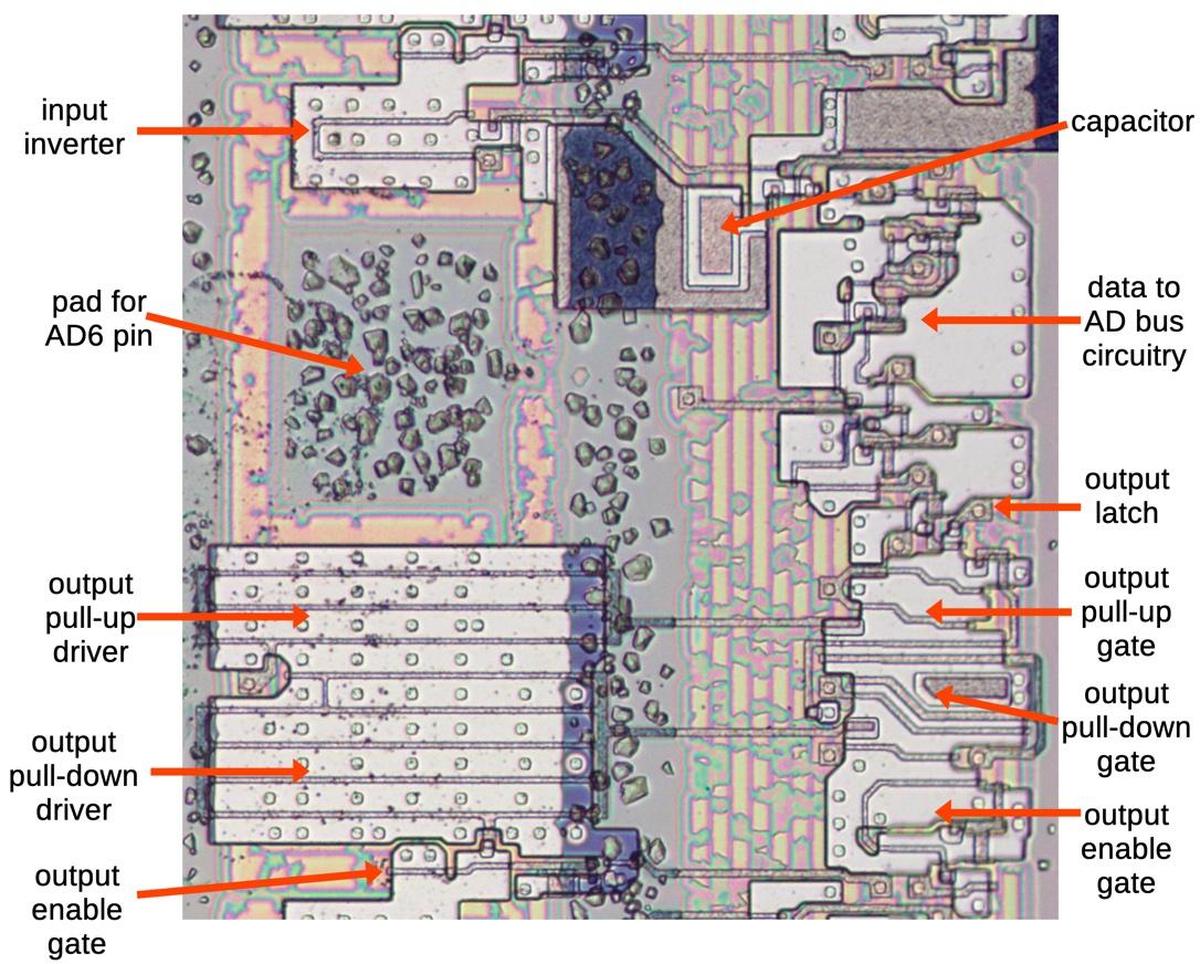
To support data input on the AD0-AD15 pins, they have a circuit to buffer the input data and transfer it to the AD bus. The incoming data bit is buffered by the two inverters and sampled when the clock is high. If the enable' signal is low, the data bit is transferred to the AD bus when the clock is low.19 The two MOSFETs act as a "superbuffer", providing enough current for the fairly long AD bus. I'm not sure what the capacitor accomplishes, maybe avoiding a race condition if the data pin changes just as the clock goes low.20
This circuit has a second role, precharging the AD bus high when the clock is low, if there's no data. Precharging a bus is fairly common in the 8086 (and other NMOS processors) because NMOS transistors are better at pulling a line low than pulling it high. Thus, it's often faster to precharge a line high before it's needed and then pull it low for a 0.21
Since pins A16-A19 are not used for data, they operate the same for reads as for writes: providing address bits and then status.
The pin circuit on the die
The diagram below shows how the pin circuitry appears on the die. The metal wiring has been removed to show the silicon and polysilicon. The top half of the image is the input circuitry, reading a data bit from the pin and feeding it to the AD bus. The lower half of the image is the output circuitry, reading an address or data bit from the AD bus and amplifying it for output via the pad. The light gray regions are doped, conductive silicon. The thin tan lines are polysilicon, which forms transistor gates where it crosses doped silicon.
A historical look at pins and timing
The number of pins on Intel chips has grown exponentially, more than a factor of 100 in 50 years. In the early days, Intel management was convinced that a 16-pin package was large enough for any integrated circuit. As a result, the Intel 4004 processor (1971) was crammed into a 16-pin package. Intel chip designer Federico Faggin22 describes 16-pin packages as a completely silly requirement that was throwing away performance, but the "God-given 16 pins" was like a religion at Intel. When Intel was forced to use 18 pins by the 1103 memory chip, it "was like the sky had dropped from heaven" and he had "never seen so many long faces at Intel." Although the 8008 processor (1972) was able to use 18 pins, this low pin count still harmed performance by forcing pins to be used for multiple purposes.
The Intel 8080 (1974) had a larger, 40-pin package that allowed it to have 16 address pins and 8 data pins. Intel stuck with this size for the 8086, even though competitors used larger packages with more pins.23 As processors became more complex, the 40-pin package became infeasible and the pin count rapidly expanded; The 80286 processor (1982) had a 68-pin package, while the i386 (1985) had 132 pins; the i386 needed many more pins because it had a 32-bit data bus and a 24- or 32-bit address bus. The i486 (1989) went to 196 pins while the original Pentium had 273 pins. Nowadays, a modern Core I9 processor uses the FCLGA1700 socket with a whopping 1700 contacts.
Looking at the history of Intel's bus timing, the 8086's complicated memory timing goes back to the Intel 8008 processor (1972). Instruction execution in the 8008 went through a specific sequence of timing states; each clock cycle was assigned a particular state number. Memory accesses took three cycles: the address was sent to memory during states T1 and T2, half of the address at a time since there were only 8 address pins. During state T3, a data byte was either transmitted to memory or read from memory. Instruction execution took place during T4 and T5. State signals from the 8008 chip indicated which state it was in.
The 8080 used an even more complicated timing system. An instruction consisted of one to five "machine cycles", numbered M1 through M5, where each machine cycle corresponded to a memory or I/O access. Each machine cycle consisted of three to five states, T1 through T5, similar to the 8008 states. The 8080 had 10 different types of machine cycle such as instruction fetch, memory read, memory write, stack read or write, or I/O read or write. The status bits indicated the type of machine cycle. The 8086 kept the T1 through T4 memory cycle. Because the 8086 decoupled instruction prefetching from execution, it no longer had explicit M machine cycles. Instead, it used status bits to indicate 8 types of bus activity such as instruction fetch, read data, or write I/O.
Conclusions
Well, address pins is another subject that I thought would be straightforward to explain but turned out to be surprisingly complicated. Many of the 8086's design decisions combine in the address pins: segmented addressing, backward compatibility, and the small 40-pin package. Moreover, because memory accesses are critical to performance, Intel put a lot of effort into this circuitry. Thus, the pin circuitry is tuned for particular purposes, especially pin A18 which is different from all the rest.
There is a lot more to say about memory accesses and how the 8086's Bus Interface Unit performs them. The process is very complicated, with interacting state machines for memory operation and instruction prefetches, as well as handling unaligned memory accesses. I plan to write more, so follow me on Twitter @kenshirriff or RSS for updates. I've also started experimenting with Mastodon recently as @[email protected] and Bluesky as @righto.com so you can follow me there too.
Notes and references
-
In the discussion, I'll often call all the address pins "AD" pins for simplicity, even though pins 16-19 are not used for data. ↩
-
The 8086's compatibility with the 8080 was somewhat limited since the 8086 had a different instruction set. However, Intel provided a conversion program called CONV86 that could convert 8080/8085 assembly code into 8086 assembly code that would usually work after minor editing. The 8086 was designed to make this process straightforward, with a mapping from the 8080's registers onto the 8086's registers, along with a mostly-compatible instruction set. (There were a few 8080 instructions that would be expanded into multiple 8086 instructions.) The conversion worked for straightforward code, but didn't work well with tricky, self-modifying code, for instance. ↩
-
To support the 8086's segment architecture, programmers needed to deal with "near" and "far" pointers. A near pointer consisted of a 16-bit offset and could access 64K in a segment. A far pointer consisted of a 16-bit offset along with a 16-bit segment address. By modifying the segment register on each access, the full megabyte of memory could be accessed. The drawbacks were that far pointers were twice as big and were slower. ↩
-
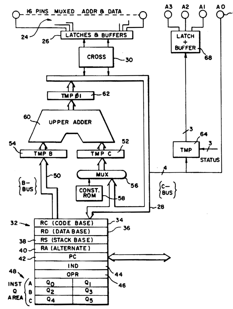
The 8086 patent provides a detailed architectural diagram of the 8086. I've extracted part of the diagram below. In most cases the diagram is accurate, but its description of the C bus doesn't match the real chip. There are some curious differences between the patent diagram and the actual implementation of the 8086, suggesting that the data pins were reorganized between the patent and the completion of the 8086. The diagram shows the address adder (called the Upper Adder) connected to the C bus, which is connected to the address/data pins. In particular, the patent shows the data pins multiplexed with the high address pins, while the low address pins A3-A0 are multiplexed with three status signals. The actual implementation of the 8086 is the other way around, with the data pins multiplexed with the low address pins while the high address pins A19-A16 are multiplexed with the status signals. Moreover, the patent doesn't show anything corresponding to what I call the AD bus; I made up that name. The moral is that while patents can be very informative, they can also be misleading.
A diagram from patent US4449184 showing the connections to the address pins. This diagram does not match the actual chip. The diagram also shows the old segment register names: RC, RD, RS, and RA became CS, DS, SS, and ES. -
The C bus is connected to the PC, OPR, and IND registers, as well as the prefetch queue, but is not connected to the segment registers. Two other buses (the ALU bus and the B bus) provide access to the segment registers. ↩
-
Swapping the bytes on the data pins is required in a few cases. The 8086 has a 16-bit data bus, so transfers are usually a 16-bit word, copied directly between memory and a register. However, the 8086 also allows 8-bit operations, in which case either the top half or bottom half of the word is accessed. Loading an 8-bit value from the top half of a memory word into the bottom half of a register uses the crossover circuit. Another case is performing a 16-bit access to an "unaligned" address, that is, an odd address so the word crosses the normal word boundaries. From the programmer's perspective, an unaligned access is permitted (unlike many RISC processors), but the hardware converts this access into two 8-bit accesses, so the bus itself never handles an unaligned access.
The 8086 has the ability to access a single memory byte out of a word, either for a byte operation or for an unaligned word operation. This behavior has some important consequences on the address pins. In particular, the low address pin AD0 doesn't behave like the rest of the address pins due to the special handling of odd addresses. Instead, this pin indicates which half of the word to transfer. The AD0 line is low (0) when the lower portion of the bus transfers a byte. Another pin, BHE (Bus High Enable) has a similar role for the upper half of the bus: it is low (0) if a byte is transferred over D15-D8. (Keep in mind that the 8086 is little-endian, so the low byte of the word is first in memory, at the even address.)
The following table summarizes how BHE and A0 work together to select a byte or word. When accessing a byte at an odd address, A0 is odd as you might expect.
↩Access type BHE A0 Word 0 0 Low byte 1 0 High byte 0 1 -
The
cbus-adbus-shiftsignal is activated duringT2, when a memory index is being updated, either the instruction pointer or theINDregister. The address adder is used to update the register and the shift undoes the 4-bit left shift applied to the adder's output. The shift is also used for theCORRmicro-instruction, which corrects the instruction pointer to account for prefetching. TheCORRmicro-instruction generates a "fake" short bus cycle in which the constant ROM and the address adder are used during T0. I discuss theCORRmicro-instruction in more detail in this post. ↩ -
I've made the timing diagram somewhat idealized so actions line up with the clock. In the real datasheet, all the signals are skewed by various amounts so the timing is more complicated. Moreover, if the memory device is slow, it can insert "wait" states between T3 and T4. (Cheap memory was slower and would need wait states.) Moreover, actions don't exactly line up with the clock. I'm also omitting various control signals. The datasheet has pages of timing constraints on exactly when signals can change. ↩
-
Instruction prefetches don't use the
INDandOPRregisters. Instead, the address is specified by the Instruction Pointer (or Program Counter), and the data is stored directly into one of the instruction prefetch registers. ↩ -
A single memory operation takes six clock cycles: two preparatory cycles to compute the address before the four visible cycles. However, if multiple memory operations are performed, the operations are overlapped to achieve a degree of pipelining. Specifically, the address calculation for the next memory operation takes place during the last two clock cycles of the current memory operation, saving two clock cycles. That is, for consecutive bus cycles, T3 and T4 overlap with TS and T0 of the next cycle. In other words, during T3 and T4 of one bus cycle, the memory address gets computed for the next bus cycle. This pipelining improves performance, compared to taking 6 clock cycles for each bus cycle. ↩
-
The
POPoperation is an example of how the address adder updates a memory pointer. In this case, the stack address is moved from the Stack Pointer to theINDregister in order to perform the memory read. As part of the read operation, theINDregister is incremented by 2. The address is then moved from theINDregister to the Stack Pointer. Thus, the address adder not only performs the segment arithmetic, but also computes the new value for theSPregister.Note that the increment/decrement of the
INDregister happens after the memory operation. For stack operations, the SP must be decremented before aPUSHand incremented after aPOP. The adder cannot perform a predecrement, so thePUSHinstruction uses the ALU (Arithmetic/Logic Unit) to perform the decrement. ↩ -
The current from an MOS transistor is proportional to the width of the gate divided by the length (the W/L ratio). Since the minimum gate length is set by the manufacturing process, increasing the width of the gate (and thus the overall size of the transistor) is how the transistor's current is increased. ↩
-
Using one transistor to pull the output high and one to pull the output low is normal for CMOS gates, but it is unusual for NMOS chips like the 8086. A normal NMOS gate only has active transistor to pull the output low and uses a depletion-mode transistor to provide a weak pull-up current, similar to a pull-up resistor. I discuss superbuffers in more detail here. ↩
-
The flip-flop is controlled by the inverted clock signal, so the output will change when the clock goes low. Meanwhile, the
enablesignal is dynamically latched by a MOSFET, also controlled by the inverted clock. (When the clock goes high, the previous value will be retained by the gate capacitance of the inverter.) ↩ -
The superbuffer AND gates are constructed on the same principle as the regular superbuffer, except with two inputs. Two transistors in series pull the output high if both inputs are high. Two transistors in parallel pull the output low if either input is low. The low-side transistors are driven by inverted signals. I haven't drawn these signals on the schematic to simplify it.
The superbuffer AND gates use large transistors, but not as large as the output transistors, providing an intermediate amplification stage between the small internal signals and the large external signals. Because of the high capacitance of the large output transistors, they need to be driven with larger signals. There's a lot of theory behind how transistor sizes should be scaled for maximum performance, described in the book Logical Effort. Roughly speaking, for best performance when scaling up a signal, each stage should be about 3 to 4 times as large as the previous one, so a fairly large number of stages are used (page 21). The 8086 simplifies this with two stages, presumably giving up a bit of performance in exchange for keeping the drivers smaller and simpler. ↩
-
The enable circuitry has some complications. For instance, I think the address pins will be enabled if a cycle was going to be T1 for a prefetch but then got preempted by a memory operation. The bus control logic is fairly complicated. ↩
-
The multiplexer is implemented with pass transistors, rather than gates. One of the pass transistors is turned on to pass that value through to the multiplexer's output. The flip-flop is implemented with two pass transistors and two inverters in alternating order. The first pass transistor is activated by the clock and the second by the complemented clock. When a pass transistor is off, its output is held by the gate capacitance of the inverter, somewhat like dynamic RAM. This is one reason that the 8086 has a minimum clock speed: if the clock is too slow, these capacitively-held values will drain away. ↩
-
The status outputs on the address pins are defined as follows: A16/S3, A17/S4: these two status lines indicate which relocation register is being used for the memory access, i.e. the stack segment, code segment, data segment, or alternate segment. Theoretically, a system could use a different memory bank for each segment and increase the total memory capacity to 4 megabytes.
A18/S5: indicates the status of the interrupt enable bit. In order to provide the most up-to-date value, this pin has a different circuit. It is updated at the beginning of each clock cycle, so it can change during a bus cycle. The motivation for this is presumably so peripherals can determine immediately if the interrupt enable status changes.
A19/S6: the documentation calls this a status output, even though it always outputs a status of 0. ↩ -
For a read, the enable signal is activated at the end of T3 and the beginning of T4 to transfer the data value to the AD bus. The signal is gated by the READY pin, so the read doesn't happen until the external device is ready. The 8086 will insert Tw wait states in that case. ↩
-
The datasheet says that a data value must be held steady for 10 nanoseconds (TCLDX) after the clock goes low at the start of T4. ↩
-
The design of the AD bus is a bit unusual since the adder will put a value on the AD bus when the clock is high, while the data pin will put a value on the AD bus when the clock is low (while otherwise precharging it when the clock is low). Usually the bus is precharged during one clock phase and all users of the bus pull it low (for a 0) during the other phase. ↩
-
Federico Faggin's oral history is here. The relevant part is on pages 55 and 56. ↩
-
The Texas Instruments TMS9900 (1976) used a 64-pin package for instance, as did the Motorola 68000 (1979). ↩
