Silicon reverse-engineering: the Intel 8086 processor's flag circuitry

Status flags are a key part of most processors, indicating if an arithmetic result is negative, zero, or has a carry, for instance. In this post, I take a close look at the flag circuitry in the Intel 8086 processor (1978), the chip that launched the PC revolution.1 Looking at the silicon die of the 8086 reveals how its flags are implemented. The 8086's flag circuitry is surprisingly complicated, full of corner cases and special handling. Moreover, I found an undocumented zero register that is used by the microcode.

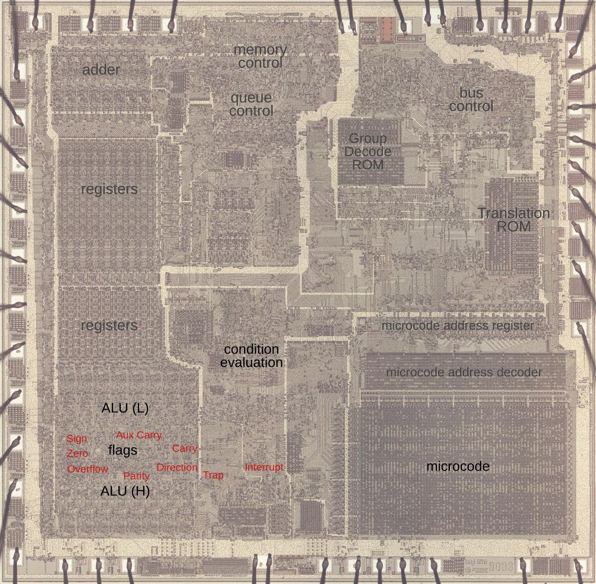
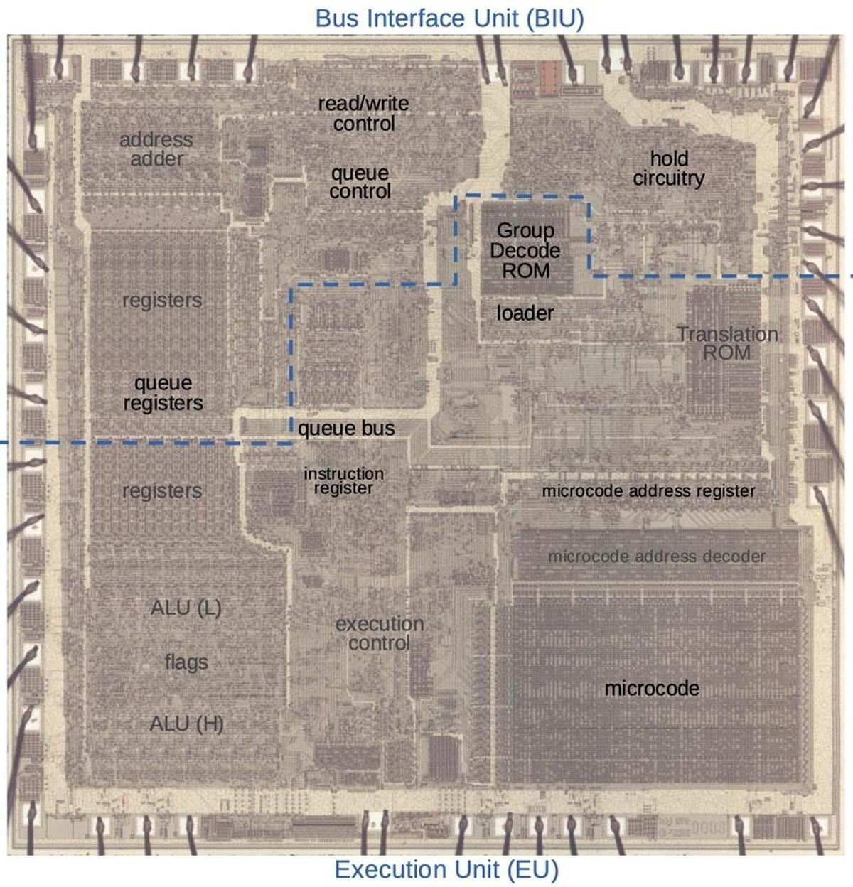
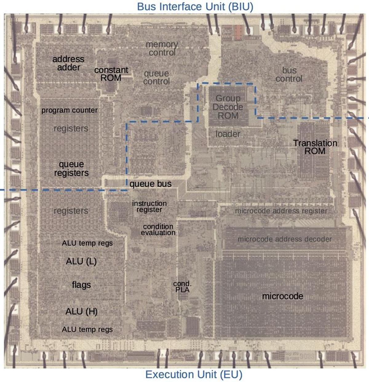
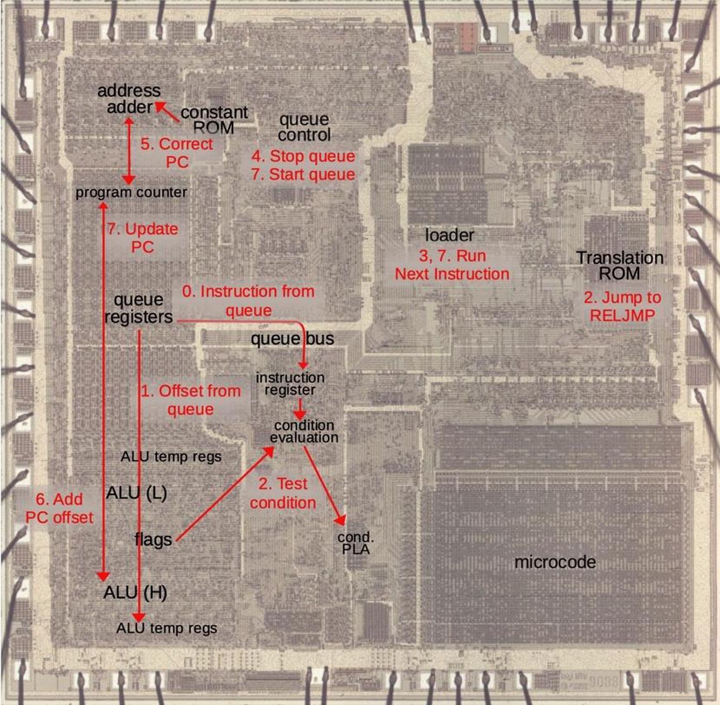
The die photo below shows the 8086 microprocessor under a microscope. The metal layer on top of the chip is visible, with the silicon and polysilicon mostly hidden underneath. Around the edges of the die, bond wires connect pads to the chip's 40 external pins. I've labeled the key functional blocks; the ones that are important to this discussion are darker and will be discussed in detail below. The Arithmetic/Logic Unit (ALU, lower left) is split in two. The circuitry for the flags is in the middle, giving it access to the ALU's results for the low byte and the high byte. I've marked each flag latch in red in the diagram below. They appear to be randomly scattered, but there are reasons for this layout.

The 8086 die under a microscope, with main functional blocks labeled. This photo shows the chip's single metal layer; the polysilicon and silicon are underneath. Click on this image (or any other) for a larger version.

The 8086 die under a microscope, with main functional blocks labeled. This photo shows the chip's single metal layer; the polysilicon and silicon are underneath. Click on this image (or any other) for a larger version.

Flags and arithmetic operations

The 8086 supports three types of arithmetic: unsigned arithmetic, signed arithmetic, and BCD (Binary-Coded Decimal) and this is a key to understanding the flags. Unsigned arithmetic uses standard binary values: a byte holds an integer value from 0 to 255, while a 16-bit word holds a value from 0 to 65535. When adding, a carry indicates that the result is too big to fit in a byte or word. (I'll use byte operations to keep the examples small; operations on words are similar.) For instance, suppose you add hex 0x60 + 0x30. The result, 0x90, fits in a byte so there is no carry. But adding 0x90 + 0x90 yields 0x120. This result doesn't fit in a byte, so the result is 0x20 with the carry flag set to 1. The carry allows additions to be chained together, like doing long decimal addition on paper. For subtraction, the carry bit indicates a borrow.

The second type of arithmetic is 2's complement, which supports negative numbers. In a signed byte, 0x00 to 0x7f represent 0 to 127, while 0x80 to 0xff represent -128 to -1. If the top bit of a signed value is set, the value is negative; this is what the sign flag indicates. The clever thing about 2's complement arithmetic is that the same instructions are used for unsigned arithmetic and 2's complement arithmetic. The only thing that changes is the interpretation. As an example of signed arithmetic, 0xff + 0x05 = 0x04 corresponds to -1 + 5 = 4. Signed arithmetic can result in overflow, though. For example, suppose you add 112 + 112: 0x70 + 0x70 = 0xe0. Although that is fine in unsigned arithmetic, in signed arithmetic that result is unexpectedly -32. The problem is that the result doesn't fit in a single signed byte. In this case, the overflow flag is set to indicate that the result overflowed. In other words, the carry flag indicates that an unsigned result doesn't fit in a byte or word, while the overflow flag indicates that a signed result doesn't fit.

The third type of arithmetic is BCD (Binary-Coded Decimal), which stores a decimal digit as a 4-bit binary value. Thus, two digits can be packed into a byte. For instance, adding 12 + 34 = 46 corresponds to 0x12 + 0x34 = 0x46 with BCD. After adding or subtracting BCD values, a special instruction is needed to perform any necessary adjustment.2 This instruction needs to know if there was a carry from the lower digit to the upper digit, i.e. a carry from bit 4 to bit 3. Many systems call this a half-carry, since it is the carry out of a half-byte, but Intel calls it the auxiliary carry flag.

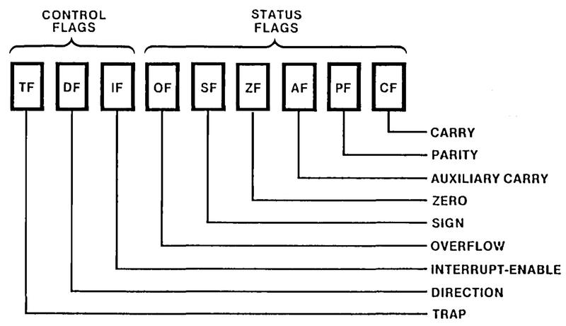
The diagram below summarizes the 8086's flags. The overflow, sign, auxiliary carry, and carry flags were discussed above. The zero flag simply indicates that the result of an operation was zero. The parity flag counts the number of 1 bits in a result byte and the flag is set if the number of 1 bits is even. At the left are the three control flags. The trap flag turns on single-stepping mode. The direction flag controls the direction of string operations. Finally, the interrupt flag enables interrupts.

The control and status flags in the 8086. Diagram from iAPX 86/88 Users Manual fig 2.9.

The control and status flags in the 8086. Diagram from iAPX 86/88 Users Manual fig 2.9.

The status flags are often used with the CMP (Compare) instruction, which performs a subtraction without storing the result. Although this may seem pointless, the status flags show the relationship between the values. For instance, the zero flag will be set if the two values are equal. Other flag combinations indicate "less than", "greater than", and other useful conditions. Loops and if statements use conditional jump instructions that test these flags. (I wrote more about 8086 conditional jumps here.)

Microcode and flags

Most people think of machine instructions as the basic steps that a computer performs. However, many processors (including the 8086) have another layer of software underneath: microcode. Instead of building the processor's control logic out of flip-flops and gates, microcode replaces much of the control logic with code. To execute a machine instruction, the computer internally executes several simpler micro-instructions, specified by the microcode. The main advantage of microcode is that it turns the design of control circuitry into a programming task instead of a difficult logic design task.

An 8086 micro-instruction is encoded into 21 bits as shown below. Every micro-instruction contains a move from a source register to a destination register, each specified with 5 bits. The meaning of the remaining bits depends on the type field, which is two or three bits long. For the current discussion, the most relevant part of the microcode is the Flag bit F at the end, which indicates that the micro-instruction will update the flags.3

The encoding of a micro-instruction into 21 bits. Based on NEC v. Intel: Will Hardware Be Drawn into the Black Hole of Copyright?

The encoding of a micro-instruction into 21 bits. Based on NEC v. Intel: Will Hardware Be Drawn into the Black Hole of Copyright?

As an example, the microcode below implements the INC (increment) and DEC (decrement) instructions. The first micro-instruction moves a word from the register specified by the instruction (indicated by M) to the ALU's temporary B register. It sets up the ALU to perform the operation specified by the instruction (indicated by XI), and indicates that the next micro-instruction (NX) is the last for this machine instruction. The second micro-instruction moves the ALU result (Σ) to the specified register (M), tells the system to run the next instruction RNI, and causes the flags (F) to be updated from the ALU result. Thus, the flags are updated with the results of the increment or decrement.

   move       action
1 M→tmpb   XI    tmpb, NX
2 Σ→M      RNI   F

This microcode is rather generic: it doesn't explicitly specify the register or the ALU operation. Instead, the gate logic determines them from the machine instruction. This illustrates the 8086's hybrid approach: although the 8086 uses microcode, the microcode is parameterized and much of the instruction functionality is implemented with gate logic. When the microcode specifies a generic Arithmetic/Logic Unit (ALU) operation, the gate logic determines from the instruction which ALU (Arithmetic/Logic Unit) operation to perform (in this case, increment or decrement). The gate logic also determines from the instruction bits which register to modify. Finally, the microcode says to update the flags, but the ALU determines how to update the flags. This hybrid approach kept the microcode small enough for 1978 technology; the microcode above supports 16 different increment and decrement instructions.

Microcode can also read or write the flags as a whole, treating the flags as a register. The first micro-instruction below stores the flags to memory (via the OPerand Register), while the second micro-instruction below loads the flags from memory. The first micro-instruction is part of the microcode for PUSHF (push flags to the stack) and interrupt handling. The second micro-instruction is used for POPF (pop flags from the stack), the interrupt return code, and the reset code. Similar micro-instructions are used for LAHF (Load AH from Flags) and SAHF (Store AH to Flags).

  F→OPR
  OPR→F

Microcode can also modify some flags directly with the micro-operations CCOF (Clear Carry and Overflow Flags), SCOF (Set Carry and Overflow Flags), and CITF (Clear Interrupt and Trap Flags). The first two are used in the microcode for multiplication and division, while the third is used in the interrupt handler.

Finally, some machine instructions are implemented directly in logic and do not use microcode at all. The CMC (Complement Carry), CLC (Clear Carry), STC (Set Carry), CLI (Clear Interrupt), STI (Set Interrupt), CLD (Clear Direction), and STD (Set Direction) instructions modify the flags directly without running any microcode. (During instruction decoding, the Group Decode ROM indicates that these instructions are implemented with logic, not microcode.)

The latch circuit that stores flags

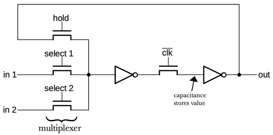
Each flag is stored in a latch circuit that holds the flag's value until it is updated. A typical flag latch has two inputs for updates: the flag value generated by the ALU, and a value from the bus when storing to all the flags. The latch also has a "hold" input to keep the existing value. (Some flags, such as carry, have more inputs, as will be described below.) A multiplexer (built from pass transistors) selects one of the inputs for the latch.

A typical latch to hold a flag. The latch is constructed from NMOS transistors and inverters. A "1" input turns on a transistor, letting its input pass through it.

A typical latch to hold a flag. The latch is constructed from NMOS transistors and inverters. A "1" input turns on a transistor, letting its input pass through it.

The latch is based on pass transistors and two inverters forming a loop. To see how it works, suppose select 1 is high. This turns on the transistor letting the in 1 value flow through the transistor and the first inverter. When clk' is high, the signal will flow through the second inverter and the output. While hold is high, the output is fed back from the output to the input, causing the latch to "remember" its value. The latch is controlled by the CPU's clock and it will only update the output when clk' is high. While clk' is low, the output will remain unchanged; the capacitance of the wire is enough to provide an input to the second inverter, a bit like dynamic RAM.4

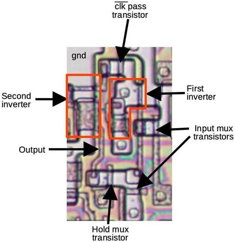
The diagram below shows how one of these latches looks on the die. The pinkish regions are doped silicon, while the brownish lines are polysilicon. A transistor gate is formed where polysilicon crosses over doped silicon. Each inverter consists of two transistors. The signal flows through the latch in roughly a counterclockwise circle, starting with one of the inputs on the right.

The latch for the Sign Flag. The metal layer was removed for this image.

The latch for the Sign Flag. The metal layer was removed for this image.

Implementation of the flags

In this section, I'll discuss each flag in detail. But first, I'll explain the circuitry common to all the flags. As explained above, microcode can treat the flags as a register, reading or writing all the flags in parallel. When the microcode specifies flags as the destination for a move, a signal is generated that I call flags-load. This signal enables the multiplexer inputs (described above) that connect the ALU bus to the flag latches, loading the bits into the latches. Conversely, when microcode specifies the flags as the source for a move, a signal is generated that I call flags-read.5 This signal connects the outputs of the flag latches to the ALU bus through pass transistors, loading the value of the flags onto the bus.

Sign flag

The sign flag is pretty simple: it stores the top bit of the ALU result, indicating a negative result. For a byte operation, this is bit 7 and for a word operation, bit 15, so some logic selects the right bit based on the instruction. (This is another example of how logic circuitry looks after the details that microcode ignores.) The output from the sign flag goes to the condition evaluation circuitry to support conditional jumps, as do the other arithmetic flags. I wrote about that recently, so I won't go into details here.

The six arithmetic status flags are updated by arithmetic operations when the microcode F bit is set. This bit generates a signal that I call arith-flag-load, indicating that the flags should be updated based on the ALU result. This signal enables the multiplexer inputs between the ALU circuitry and the flag latches. There is an inconvenient special case: rotate instructions only update the overflow and carry flags for compatibility with the 8080 processor.6 To support this, a rotate instruction blocks the arith-flag-load signal for the sign, parity, zero, and auxiliary carry flags. Again, this is handled by gates, rather than microcode.

Zero flag

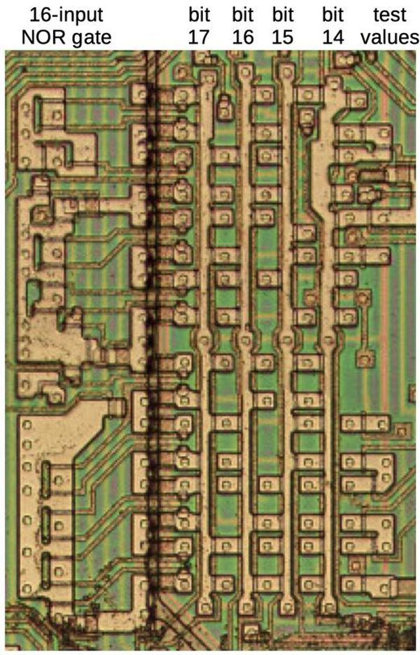
The zero flag is also straightforward. It indicates that the result byte or word is all zeros, for a byte or word operation respectively. An 8-input NOR gate at the top of the flags circuitry determines if the lower byte is all zeros, while an 8-input NOR gate at the bottom of the flags circuitry tests the upper byte. These NOR gates are spread out and span the width of the ALU, essentially a wire that is pulled low by any result bits that are high. The zero flag is set based on the low byte or the whole word, for a byte instruction or word instruction respectively.

There is a second zero flag, hidden from the programmer. This zero flag always tests the full 16-bit result, so I'll call it Z16. The other key difference is that the Z16 flag is updated on every ALU micro-operation, rather than under the control of the F bit. Thus, the Z16 flag can be updated without interfering with the programmer-visible zero flag. This makes it useful for internal microcode operations, such as loops.

Parity flag

The parity flag is conceptually simple, but it is fairly expensive to implement in hardware as it requires exclusive-oring the eight bits of the result byte together. This is implemented with seven XOR circuits.7 Since each XOR circuit is implemented with two logic gates, the raw parity calculation requires 14 gates. Only 8-bit parity is supported, even if a word operation is performed.8

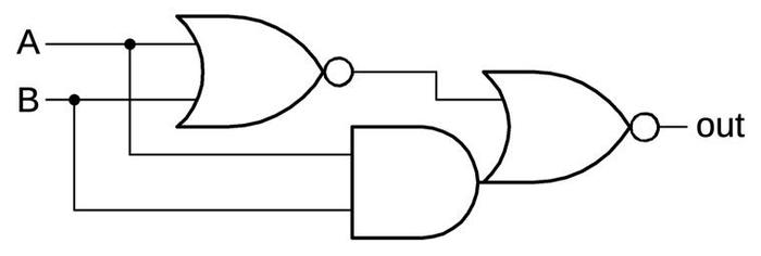
The schematic below shows how an XOR circuit is implemented. It uses two gates; due to the properties of NMOS transistors, the AND-NOR gate is implemented as a single gate. To see how it works, suppose A and B are 0. The first NOR gate will output 1, forcing the output to 0. If A and B are both 1, the AND gate will force the output to 0. Otherwise the output is 1, providing the XOR function. The key point is that XOR is fairly costly compared to other logic functions.

Schematic of an XOR circuit.

Schematic of an XOR circuit.

Auxiliary carry flag

The auxiliary carry starts off simple, but is complicated by the decimal adjust instructions. In most cases, the auxiliary carry is carry-out from bit 3 of the ALU (i.e. the half-carry). For subtraction, the flag must be inverted to indicate a borrow, so the half-carry is exclusive-or'd with a subtraction signal.

However, the decimal adjust instructions (DAA, DAS, AAA, AAS) use the auxiliary carry and also modify the auxiliary carry when performing a decimal adjust. After an addition or subtraction, the decimal adjust instructions produce a correction value if necessary. If the lower digit is more than 9 or the auxiliary carry is set, the value 6 is added (or subtracted) from the accumulator.9 The DAA and AAA instructions also test if a correction of 0x60 is needed for the upper digit. The correction signals are wired to the ALU bus to generate the correction factor of 0x06, 0x60, or 0x66 for an adjustment ALU operation. The correction signal for the low digit is stored as the auxiliary carry flag.

Carry flag

The carry flag is surprisingly complex, with five inputs to the carry flag input multiplexer. The first input is the carry value for an ALU operation:10 the top bit of the ALU result (bit 7 or 15 for a byte or word operation). However, for a subtraction the carry is inverted to form the borrow. But for a DAA or DAS decimal adjust operation, the carry comes from the high-digit correction signal. And for an AAA or AAS ASCII adjust operation, the carry comes from the low-digit correction signal. These cases are determined with logic gates and fed into a single multiplexer input.

Another multiplexer input supports the CMC (Complement Carry) instruction by feeding in the current flag value but inverted. The STC and CLC (Set Carry and Clear Carry) instructions are implemented by feeding the low bit of the instruction into a different multiplexer input. This input also supports the micro-instructions SCOF (Set Carry, Overflow Flags), CCOF (Clear Carry, Overflow Flags), and RCY (Reset Carry).

The rotate and shift instructions have complex interactions with the carry flag, since bits are shifted in and out of the carry flag. For a shift or rotate, a separate multiplexer input provides the bit for the carry flag latch. For a right shift or rotate, the lowest bit of the ALU argument is fed into the carry flag. For a left shift or rotate, the carry out of bit 15 or bit 7 is fed into the carry flag; this was the highest bit for a word or byte operation respectively.

The output from the carry flag is fed into the ALU's carry-in for the ADC (Add with Carry), SBB (Subtract with Borrow), and RCL (Rotate through Carry, Left) instructions; the carry is inverted for SBB to form the borrow. For an RCR (Rotate through Carry, Right), the carry is fed into the ALU's output bit 7 or 15 (for a byte or word operation respectively).

Overflow flag

The circuitry for the overflow flag is fairly complicated, as there are multiple cases. For an arithmetic operation, the overflow flag indicates a signed overflow. The overflow is computed as the exclusive-or of the carry-in to the top bit and the carry-out from the top bit, selected for a byte or word operation. (I explained the mathematics behind this earlier.)

For a shift or rotate, however, the overflow flag indicates that the shifted value changed sign. The ALU implements left shifts and rotates by passing bits as carries so the old sign bit is the carry-out from the top bit, while the new sign bit is the carry-in to the top bit. Thus, the standard arithmetic overflow circuit also handles left shifts and rotates. On the other hand, for a shift or rotate right, the top two bits of the result are exclusive-or'd together to see if they are different: bits 6 and 7 for a byte shift and bits 14 and 15 for a word shift. (The second-from-the-top bit was the sign bit before the shift.)

Finally, two micro-instructions affect the flag: CCOF (Clear Carry and Overflow Flags) and SCOF (Set Carry and Overflow Flags). All these different sources for the overflow flag are combined in logic gates, rather than a complex multiplexer like the carry flag used.

Direction flag

The three remaining flags are "control" flags: rather than storing the status of an ALU operation, these flags control the CPU's behavior. The direction flag controls the direction of string operations that scan through memory: auto-incrementing or auto-decrementing. This is implemented by feeding the direction flag into the Constant ROM to determine the increment value applied to the SI and DI registers. The direction flag is set or cleared through the STD and CLD instructions (Set Direction and Clear Direction). For these instructions, the low bit of the instruction is passed into the flag to set or clear it as appropriate.

Interrupt flag

The output from the interrupt flag goes to the interrupt handling circuitry to enable or disable interrupts. This flag is set or cleared by a programmer through the STI and CLI instructions. For the STI and CLI instructions, the low bit of the instruction is passed into the flag to set or clear it as appropriate. Microcode can clear the interrupt flag and the trap flag (discussed below) with the CITF (Clear Interrupt and Trap Flag) micro-instruction. This is used in the interrupt handler to disable subsequent interrupts and traps. The CITF micro-instruction is implemented with a separate input to the flag latch.

Trap flag

The trap flag turns on single-stepping for debugging. With the trap flag on, every instruction generates an interrupt. This flag doesn't have machine instructions to modify it directly. Instead, the programmer must mess around with the PUSHF and POPF instructions to put all the flags on the stack and modify the flag bit there (details). Like the interrupt flag, the trap flag has an input to clear it if the CITF micro-instruction is active.

Layout of the flag circuitry

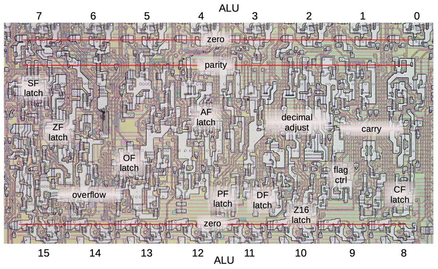
The diagram below shows the circuitry for the flags on the die, with the approximate location of each flag indicated. ALU bits 7 through 0 are above this circuitry and ALU bits 15 through 8 are below. The zero gates stretch the length of the ALU at the top and bottom, while the parity gates are near the low byte of the ALU. The flag circuitry appears highly irregular on the die because each flag has different circuitry. However, the circuitry for a flag is generally near the appropriate bit that receives the flag, so the layout is not as arbitrary as it may seem. For instance, the sign flag is affected by bit 7 or 15 of the ALU result and is loaded or stored to bit 7, so it is at the left. The trap and interrupt flags are outside the ALU, to the right of this image.

Closeup of the circuitry on the die that implements the flags. The metal layer has been removed to show the polysilicon and silicon underneath.

Closeup of the circuitry on the die that implements the flags. The metal layer has been removed to show the polysilicon and silicon underneath.

The history behind the 8086 flags11

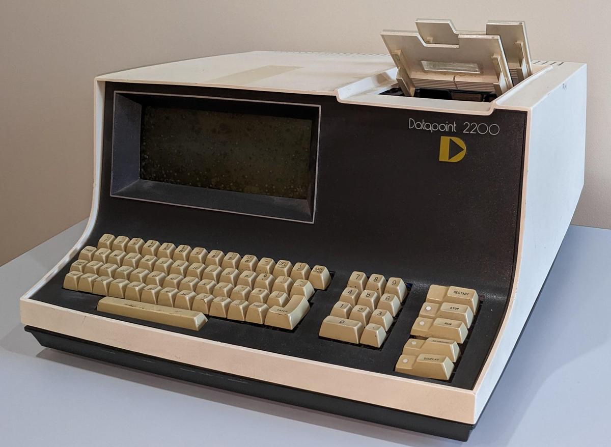
The Datapoint 2200 (1970) is a desktop computer that was sold as a "programmable terminal". Although mostly forgotten now, the Datapoint 2200 is one of the most influential computers ever, as it led to the 8086 processor and thus the modern x86 architecture. For flags, the Datapoint 2200 had four "control flip-flops": carry/borrow,12 zero, sign, and parity. These were not bits in a register and could not be accessed directly. Instead, conditional jumps, subroutine calls, or subroutine returns could be performed based on the status of one of these flip-flops. Because the Datapoint 2200 was used as a terminal, and terminal protocols often used parity, implementing parity in hardware was a useful feature.

But how did the Datapoint 2200 lead to the 8086? The Datapoint 2200 was created before the microprocessor, so its processor was a large board of TTL chips. Datapoint asked Intel and Texas Instruments if they could replace this TTL processor with a single chip. Texas Instruments created the TMX 1795, the first 8-bit microprocessor. Intel created the 8008 shortly after. Both chips copied the instruction set and architecture of the 2200. Datapoint didn't like either chip and stuck with TTL. Texas Instruments couldn't find a customer for the TMX 1795 and abandoned it. Intel, on the other hand, marketed the 8008 as a general-purpose microprocessor, essentially creating the microprocessor industry. Since the 8008 copied the Datapoint 2200, it kept the four status flip-flops.

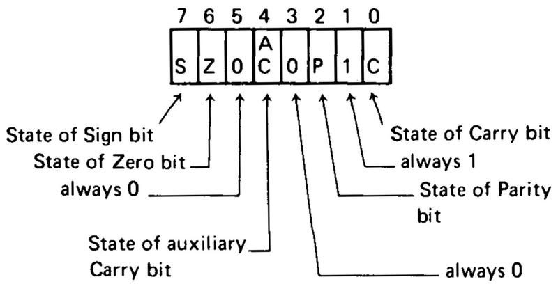
In 1974, Intel created the 8080 microprocessor, an improvement of the 8008. The 8080 kept the flags from the 8008 and added the auxiliary carry. Moreover, the flags could be accessed as a byte, making the flags appear like a register. The 8080 defined specific values for the unused flag bits. These decisions have persisted into the modern x86 architecture.13

Structure of the 8080 flags when saved on the stack. From 8080 Assembly Language Programming Manual.

Structure of the 8080 flags when saved on the stack. From 8080 Assembly Language Programming Manual.

The 8086 was designed to be backward compatible with the 8080, at least at the assembly language level.14 To support this, the 8086 kept the 8080's flag byte unchanged, putting additional flags in the high byte, as shown below. Thus, the selection, layout, and behavior of the 8086 flags (and thus x86) are largely historical accidents going back to the 8080, 8008, and Datapoint 2200 processors.

Arrangement of the 8086 flags in the word. The shaded flags match the 8080/8085 flags. Diagram from iAPX 86/88 Users Manual fig 2.10.

Arrangement of the 8086 flags in the word. The shaded flags match the 8080/8085 flags. Diagram from iAPX 86/88 Users Manual fig 2.10.

Conclusions

You might expect flags to be a simple part of a CPU, but the 8086's flags are surprisingly complex. About 1/3 of the ALU is devoted to flag computation and storage. Each flag is implemented with completely different circuitry. The 8086 is a CISC processor (Complex Instruction Set Computer), where the instruction set is designed to be powerful and to minimize the gap between machine language and high-level languages.15 This can be seen in the implementation of the flags, which are full of special cases to increase their utility with different instructions.16 In contrast, a RISC (Reduced Instruction Set Computer) simplifies the instruction set to make each instruction faster. This philosophy also affects the flags: for example, the ARM-1 processor (1985) has four arithmetic flags compared to the 8086's six flags. The behavior of the ARM flags is simpler, and the ARM doesn't deal with byte versus word operations. It also doesn't have instructions like decimal adjust that have complex flag behavior. This simplicity is reflected in the simpler and more regular circuitry of the ARM-1 flags, which I reverse-engineered here.

I've written multiple posts on the 8086 so far and plan to continue reverse-engineering the 8086 die so follow me on Twitter @kenshirriff or RSS for updates. I've also started experimenting with Mastodon recently as @oldbytes.space@kenshirriff.

Notes and references

  1. Strictly speaking, the Intel 8088 launched the PC revolution as it was the processor in the first IBM PC. But internally the 8086 and 8088 are almost identical, so everything in this post applies to the 8088 as well. (The 8088 has an 8-bit bus compared to the 8086's 16-bit bus. As a result, the bus interface circuitry is different. The 8088 has a 4-byte prefetch queue compared to the 8086's 6-byte prefetch queue. And there are a few microcode changes. Apart from these changes, the dies are essentially identical.) 

  2. Since BCD arithmetic is performed using the binary addition and subtraction instructions, an adjustment may be required. For instance, consider adding 19 + 18 = 37 using BCD: 0x19 + 0x18 = 0x31 rather than the desired 0x37. Adding an adjustment factor of 6 yields the desired answer, taking into account the carry from the low digit. The BCD adjustment instructions are DAA (Decimal Adjust after Addition), DAS (Decimal Adjust after Subtraction), AAA (ASCII Adjust after Addition), and AAS (ASCII Adjust after Subtraction). (I wrote about the DAA instruction in detail here.) 

  3. Unlike other arithmetic and logic instructions, the NOT instruction does not change any of the flags. The designer of the 8086 states that this was an oversight. (See page 98 in "The 8086/8088 Primer".) Looking at the microcode shows that the microcode F bit was omitted in the implementation of NOT. I think that this "goof" also prevented the NOT and NEG microcode from being merged, wasting four micro-instructions. 

  4. Most of the latches in the 8086 have two pass transistors: one driven by clk and one driven by clk'. This makes the circuit function like an edge-triggered flip-flop, only transitioning on the edge of the clock. The flag latches, on the other hand, gate the multiplexer input controls so they are only active when clk is high. Thus, the two inverters are connected alternately during clk and clk'

  5. The connection from flag outputs to the ALU bus is more complex than simple pass transistors. For performance reasons, the ALU bus is charged high during the clock' phase of the clock. Then, any bits that should be 0 are pulled low during the high clock phase. (The motivation is that NMOS transistors can pull a line low faster than they can pull it high.) To support this, each inverted flag output drives a transistor connected to ground, and the output from this transistor is connected to the ALU bus through a pass transistor. 

  6. The 8080 processor has four rotate instructions, while the 8086 adds three shift instructions. The new shift instructions update the arithmetic flags according to the result. However, the 8080's rotate instructions only updated the carry flag, leaving the other flags unchanged. For backward compatibility, the 8086 preserves this behavior for the rotate instructions, not modifying the other flags inherited from the 8080. Since the 8086's overflow flag didn't exist in the 8080, the 8086 can update the overflow flag for rotate instructions without breaking compatibility, even though it's not obvious what "overflow" means in the case of a rotate. (The 8080's behavior of only updating the carry flag for shifts dates back to the Datapoint 2200.)

    Curiously, The 8086 Family User's Manual shows SHR and SAL/SHL as updating just the overflow and carry flags (pages 2-265 and 2-66), contradicting the text (page 2-39). 

  7. The 8086 implements the parity computation by XORing pairs of bits. The pairs are then combined in sequence: (((bit0⊕bit1)⊕(bit2⊕bit3))⊕(bit4⊕bit5))⊕(bit6⊕bit7). Combining the terms in a tree-like arrangement would have saved gate delays, but apparently wasn't necessary. 

  8. The parity flag only examines the low byte of the result, even for a 16-bit operation, making it unusual compared to the other flags. The motivation is probably that the parity flag was only supported for backward compatibility and not considered particularly useful. Even in modern 64-bit Intel processors, the parity flag only examines the least-significant byte. 

  9. The decimal adjust circuitry uses a gate circuit to test if the lower digit is greater than nine. Specifically, it uses the expression: bit3•(bit2+bit1). In other words, if the ALU input has 8 and either 4 or 2 or both.

    The logic to determine if the upper digit needs a correction is more complex: carry+bit7•(bit6+bit5+bit4•af9), where af9 indicates that AF is not set and the lower digit is more than 9. This tests if the upper digit is greater than nine, but also handles the case where the upper digit is 9 and adjusting the lower digit will increase it.

    The DAA instruction on the 8086 has slightly different behavior from the DAA instruction on x86 in a few cases. For example, 0x9a + 0x02 = 0x9c; DAA converts this to 0xa2 on the 8086, but 0x02 on x86. Since 0x9a is not a valid BCD value, this is technically an undefined case, but it is interesting that there is a difference. Perhaps this behavior was inherited from the 8080; if anyone has an 8080 available, perhaps they can test this case. (I wrote about the x86 DAA behavior in detail here.) 

  10. One special case is that the increment and decrement instructions affect all the arithmetic flags except for carry. This is implemented by blocking the carry-flag update for an increment or decrement instruction. The motivation is to allow a loop counter to be updated without disturbing the carry flag. This behavior was first implemented in the 8008 processor. 

  11. The book "Computer Architecture", Blaauw and Brooks, contains a detailed discussion of different approaches for condition flags, pages 353-358. Some processors, such as the IBM 704 (1954), don't explicitly store flags, but test and branch in a single instruction. Storing conditions as 1-bit values (as in the 8086) is called an "indicator". An alternative is the "condition code", which encodes mutually-exclusive condition values into a smaller number of bits, as in System/360 (1964). For example, addition stores four conditions (zero, negative, positive, or overflow) encoded into two bits, rather than separate zero, sign, and overflow flags. Other alternatives are where to store the conditions: in "working store" (i.e. a regular register), in memory, in a unique indicator (i.e. a flags register), or in a shared condition register (e.g. System/360). The point is that while the typical microprocessor approach of storing flags in a flag register may seem natural, many alternatives have been tried in different systems. 

  12. For subtraction, a borrow flag can be defined in different ways. The Datapoint 2200 and descendants store the borrow bit in the carry flag. This approach was also used by the 6800 and 68000 processors. The alternative is to store the complement of the borrow bit in the carry flag, since this maps more naturally onto twos-complement arithmetic. This approach was used by the IBM System/360 mainframe and the 6502 and ARM processors. 

  13. The positions of the 8080's flags in the byte are not arbitrary but have some logic. When performing multi-byte additions, the carry flag gets added into the low bit of the next byte, so it makes sense to put the carry flag in bit 0. Likewise, the auxiliary carry flag is in bit 4, since that is the bit it is added into. The sign bit is bit 7 of the result, so it makes sense to put the sign bit in bit 7 of the flags. As for the zero and parity flags, and the values of the unused flag bits, I don't have an explanation for those. 

  14. The 8086 was designed to provide an upgrade path from the 8080, so it inherited many instructions and architectural features along with the change from 8 bits to 16 bits. The two processors were not binary compatible or even directly compatible at the assembly code level. Instead, assembly code for the 8080 could be converted to 8086 assembly via a program called CONV-86, which would usually require manual cleanup afterward. Many of the early programs for the 8086 were conversions of 8080 programs. 

  15. The terms RISC and CISC are vague, and there are many different definitions. I'm not looking to debate definitions. 

  16. The motivation behind how 8086 instructions affect the flags is given in The 8086/8088 Primer, by Stephen Morse, the creator of the 8086 instruction set. It turns out that there are good reasons for the flags to have special-case behavior for various instructions. 

Understanding the x86's Decimal Adjust after Addition (DAA) instruction

I've been looking at the DAA machine instruction on x86 processors, a special instruction for binary-coded decimal arithmetic. Intel's manuals document each instruction in detail, but the DAA description doesn't make much sense. I ran an extensive assembly-language test of DAA on a real machine to determine exactly how the instruction behaves. In this blog post, I explain how the instruction works, in case anyone wants a better understanding.

The DAA instruction

The DAA (Decimal Adjust AL1 after Addition) instruction is designed for use with packed BCD (Binary-Coded Decimal) numbers. The idea behind BCD is to store decimal numbers in groups of four bits, with each group encoding a digit 0-9 in binary. You can fit two decimal digits in a byte; this format is called packed BCD. For instance, the decimal number 23 would be stored as hex 0x23 (which turns out to be decimal 35).

The 8086 doesn't implement BCD addition directly. Instead, you use regular binary addition and then DAA fixes the result. For instance, suppose you're adding decimal 23 and 45. In BCD these are 0x23 and 0x45 with the binary sum 0x68, so everything seems straightforward. But, there's a problem with carries. For instance, suppose you add decimal 26 and 45 in BCD. Now, 0x26 + 0x45 = 0x6b, which doesn't match the desired answer of 0x71. The problem is that a 4-bit value has a carry at 16, while a decimal digit has a carry at 10. The solution is to add a correction factor of the difference, 6, to get the correct BCD result: 0x6b + 6 = 0x71.

Thus, if a sum has a digit greater than 9, it needs to be corrected by adding 6. However, there's another problem. Consider adding decimal 28 and decimal 49 in BCD: 0x28 + 0x49 = 0x71. Although this looks like a valid BCD result, it is 6 short of the correct answer, 77, and needs a correction factor. The problem is the carry out of the low digit caused the value to wrap around. The solution is for the processor to track the carry out of the low digit, and add a correction if a carry happens. This flag is usually called a half-carry, although Intel calls it the Auxiliary Carry Flag.2

For a packed BCD value, a similar correction must be done for the upper digit. This is accomplished by the DAA (Decimal Adjust AL after Addition) instruction. Thus, to add a packed BCD value, you perform an ADD instruction followed by a DAA instruction.

Intel's explanation

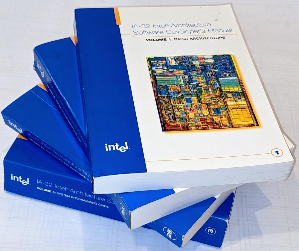
The Intel Software Developer's Manuals. These are from 2004, back when Intel would send out manuals on request.

The Intel Software Developer's Manuals. These are from 2004, back when Intel would send out manuals on request.

The Intel 64 and IA-32 Architectures Software Developer Manuals provide detailed pseudocode specifying exactly what each machine instruction does. However, in the case of DAA, the pseudocode is confusing and the description is ambiguous. To verify the operation of the DAA instruction on actual hardware, I wrote a short assembly program to perform DAA on all input values (0-255) and all four combinations of the carry and auxiliary flags.3 I tested the pseudocode against this test output. I determined that Intel's description is technically correct, but can be significantly simplified.

The manual gives the following pseudocode; my comments are in green.

IF 64-Bit Mode
  THEN
    #UD;  Undefined opcode in 64-bit mode
  ELSE
    old_AL := AL; AL holds input value
    old_CF := CF; CF is the carry flag
    CF := 0;
    IF (((AL AND 0FH) > 9) or AF = 1) AF is the auxiliary flag
      THEN
        AL := AL + 6;
        CF := old_CF or (Carry from AL := AL + 6); dead code
        AF := 1;
      ELSE
        AF := 0;
      FI;
    IF ((old_AL > 99H) or (old_CF = 1))
      THEN
        AL := AL + 60H;
        CF := 1;
      ELSE
        CF := 0;
    FI;
FI;

Removing the unnecessary code yields the version below, which makes it much clearer what is going on. The low digit is corrected if it exceeds 9 or if the auxiliary flag is set on entry. The high digit is corrected if it exceeds 9 or if the carry flag is set on entry.4 At completion, the auxiliary and carry flags are set if an adjustment happened to the corresponding digit.5 (Because these flags force a correction, the operation never clears them if they were set at entry.)

IF 64-Bit Mode
  THEN
    #UD;
  ELSE
    old_AL := AL;
    IF (((AL AND 0FH) > 9) or AF = 1)
      THEN
        AL := AL + 6;
        AF := 1;
      FI;
    IF ((old_AL > 99H) or CF = 1)
      THEN
        AL := AL + 60H;
        CF := 1;
    FI;
FI;

History of BCD

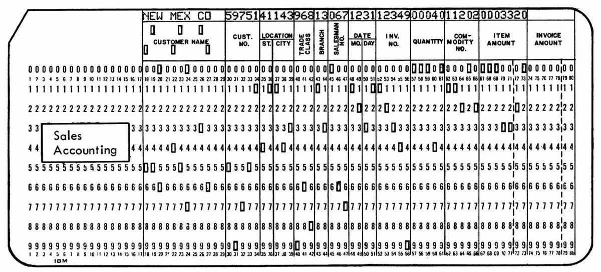
The use of binary-coded decimal may seem strange from the modern perspective, but it makes more sense looking at some history. In 1928, IBM introduced the 80-column punch card, which became very popular for business data processing. These cards store one decimal digit per column, with each digit indicated by a single hole in row 0 through 9.6 Even before digital computers, businesses could perform fairly complex operations on punch-card data using electromechanical equipment such as sorters and collators. Tabulators, programmed by wiring panels, performed arithmetic on punch cards using electromechanical counting wheels and printed business reports.

Example card, from IBM 29 Card Punch Reference Manual.

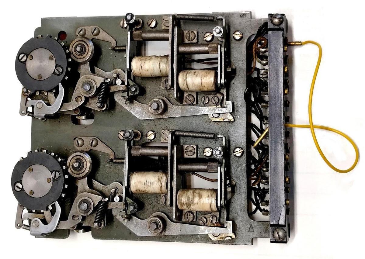
These calculations were performed in decimal. Decimal fields were read off punch cards, added with decimal counting wheels, and printed as decimal digits. Numbers were not represented in binary, or even binary-coded decimal. Instead, digits were represented by the position of the hole in the card, which controlled the timing of pulses inside the machinery. These pulses rotated counting wheels, which stored their totals as angular rotations, a bit like an odometer.

A counter unit from an IBM accounting machine (tabulator). The two wheels held two digits. The electromagnets (white) engaged and disengaged the clutch so the wheel would advance the desired number of positions.

A counter unit from an IBM accounting machine (tabulator). The two wheels held two digits. The electromagnets (white) engaged and disengaged the clutch so the wheel would advance the desired number of positions.

With the rise of electronic digital computers in the 1950s, you might expect binary to take over. Scientific computers used binary for their calculations, such as the IBM 701 (1952). However, business computers such as the IBM 702 (1955) and the IBM 1401 (1959) operated on decimal digits, typically stored as binary-coded decimal in 6-bit characters. Unlike the scientific computers, these business computers performed arithmetic operation in decimal.

The main advantage of decimal arithmetic was compatibility with decimal fields stored in punch cards. Second, decimal arithmetic avoided time-consuming conversions between binary and decimal, a benefit for applications that were primarily input and output rather than computation. Finally, decimal arithmetic avoided the rounding and truncation problems that can happen if you use floating-point numbers for accounting calculations.

The importance of decimal arithmetic to business can be seen in its influence on the COBOL programming language, very popular for business applications. A data field was specified with the PICTURE clause, which specified exactly how many decimal digits each field contained. For instance PICTURE S999V99 specified a five-digit number (five 9's) with a sign (S) and implied decimal point (V). (Binary fields were an optional feature.)

In 1964, IBM introduced the System/360 line of computers, designed for both scientific and business use, the whole 360° of applications. The System/360 architecture was based on 32-bit binary words. But to support business applications, it also provided decimal data structures. Packed decimal provided variable-length decimal fields by putting two binary-coded decimal digits per byte. A special set of arithmetic instructions supported addition, subtraction, multiplication, and division of decimal values.

The System/360 Model 50 in a datacenter. The console and processor are at the left. An IBM 1442 card reader/punch is behind the IBM 1052 printer-keyboard that the operator is using. At the back, another operator is loading a tape onto an IBM 2401 tape drive. Photo from IBM.

The System/360 Model 50 in a datacenter. The console and processor are at the left. An IBM 1442 card reader/punch is behind the IBM 1052 printer-keyboard that the operator is using. At the back, another operator is loading a tape onto an IBM 2401 tape drive. Photo from IBM.

With the introduction of microprocessors, binary-coded decimal remained important. The Intel 4004 microprocessor (1971) was designed for a calculator, so it needed decimal arithmetic, provided by Decimal Adjust Accumulator (DAA) instruction. Intel implemented BCD in the Intel 8080 (1974).7 This processor implemented an Auxiliary Carry (or half carry) flag and a DAA instruction. This was the source of the 8086's DAA instruction, since the 8086 was designed to be somewhat compatible with the 8080.8 The Motorola 6800 (1974) has a similar DAA instruction, while the 68000 had several BCD instructions. The MOS 6502 (1975), however, took a more convenient approach: its decimal mode flag automatically performed BCD corrections. This on-the-fly correction approach was patented, which may explain why it didn't appear in other processors.9

The use of BCD in microprocessors was probably motivated by applications that interacted with the user in decimal, from scales to video games. These motivations also applied to microcontrollers. The popular Texas Instruments TMS-1000 (1974) didn't support BCD directly, but it had special case instructions like A6AAC (Add 6 to accumulator) to make BCD arithmetic easier. The Intel 8051 microcontroller (1980) has a DAA instruction. The Atmel AVR (1997, used in Arduinos) has a half-carry flag to assist with BCD.

Binary-coded decimal has lost popularity in newer microprocessors, probably because the conversion time between binary and decimal is now insignificant. The ill-fated Itanium, for instance, didn't support decimal arithmetic. RISC processors, with their reduced instruction sets, cast aside less-important instructions such as decimal arithmetic; examples are ARM 1985), MIPS (1985), SPARC (1987), PowerPC (1992), and RISC-V (2010). Even Intel's x86 processors are moving away from the DAA instruction; it generates an invalid opcode exception in x86-64 mode. Rather than BCD, IBM's POWER6 processor (2007) supports decimal floating point for business applications that use decimal arithmetic.

Conclusions

The DAA instruction is complicated and confusing as described in Intel documentation. Hopefully the simplified code and explanation in this post make the instruction a bit easier to understand.

Follow me on Twitter @kenshirriff or RSS for updates. I've also started experimenting with Mastodon recently as @oldbytes.space@kenshirriff. I wrote about the 8085's decimal adjust circuitry in this blog post.

Notes and references

  1. The AL register is the low byte of the processor's AX register. The DAA instruction only operates on a byte; there are no 16-bit or 32-bit versions. 

  2. The AAA (ASCII Adjust after Addition) and AAS (ASCII Adjust after Subtraction) instructions perform corrections for unpacked BCD: a single digit per byte. Dealing with a single digit, these instructions are considerably simpler. These operations don't have much to do with ASCII except that they ignore and clear the upper 4 bits. Since ASCII represents the characters 0 through 9 with the values 0x30 through 0x39, ASCII characters can be used as input and the result will be a BCD digit.

    The DAS (Decimal Adjust AL after Subtraction) instruction is similar to DAA except that it applies the correction after subtraction, subtracting the correction. I'm going to focus on DAA in this article since the other instructions are similar. 

  3. My test code and results are on GitHub. The results should be the same on any x86 processor, but I did the test on a Pentium Dual-Core E5300 CPU.

    My DAA test cases include values that couldn't result from a "real" BCD addition. For example, the input 0x04 with AF set can't be generated by adding two BCD numbers because even 9+9 doesn't get the result up to carry + 4. Not surprisingly, DAA doesn't return a valid BCD result in this case, yielding 0x0a. 

  4. You might wonder why the code tests if old_AL>99H, rather than simply checking the upper digit. The reason is that the low digit can cause a half-carry during correction, messing up the upper digit. This half-carry can only happen if the lower digit is greater than nine. The upper digit would only become too big if it were 9. Thus, this case only happens if the old AL is more than 0x99. 

  5. The carry flag value produced by DAA may seem arbitrary, but it is the value necessary for performing multi-byte additions, where the carry from one addition is added to the next addition. (This is just like handling carries when performing long addition by hand.) Specifically, you want the carry set if the result has a carry-out (result > 99). This happens if the original addition produces a carry, or if the DAA operation generates a result > 99. The latter case corresponds to an adjustment of the upper digit. 

  6. Punch cards were introduced in the late 1800s for the US Census and went through various formats until most companies standardized on the 80-column card. Support for alphanumeric values was added around 1932, but I'm not going to go into that. 

  7. The earlier Intel 8008 microprocessor didn't have decimal arithmetic support because its instruction set and architecture copied the Datapoint 2200 desktop computer (1971), which did not provide decimal arithmetic. Since the Datapoint 2200 was designed as a "programmable terminal", it primarily dealt with characters and BCD was irrelevant to it. 

  8. The 8086 was designed to provide an upgrade path from the 8080, so it inherited many instructions and architectural features along with the change from 8 bits to 16 bits. The two processors were not binary compatible or even directly compatible at the assembly code level. Instead, assembly code for the 8080 could be converted to 8086 assembly via a program called CONV-86, which would usually require manual cleanup afterward. Many of the early programs for the 8086 were conversions of 8080 programs. ↩ 

  9. The Ricoh 2A03 (1983) was a microprocessor created for the NES video game system. It was a clone of the 6502 except that it omitted the decimal adjust feature, presumably to avoid patent infringement. 

Reverse-engineering the Intel 8086 processor's HALT circuits

The 8086 processor was introduced in 1978 and has greatly influenced modern computing through the x86 architecture. One unusual instruction in this processor is HLT, which stops the processor and puts it in a halt state. In this blog post, I explain in detail how the halt circuitry is implemented and how it interacts with the 8086's architecture.

The die photo below shows the 8086 microprocessor under a microscope. The metal layer on top of the chip is visible, with the silicon and polysilicon mostly hidden underneath. Around the edges of the die, bond wires connect pads to the chip's 40 external pins. I've labeled the key functional blocks; the ones that are important to this discussion are darker and will be discussed in detail below. Architecturally, the chip is partitioned into a Bus Interface Unit (BIU) at the top and an Execution Unit (EU) below. The BIU handles memory accesses, while the Execution Unit (EU) executes instructions. Both are stopped by a halt instruction.

The 8086 die under a microscope, with main functional blocks labeled. This photo shows the chip's single metal layer; the polysilicon and silicon are underneath. Click on this image (or any other) for a larger version.

The 8086 die under a microscope, with main functional blocks labeled. This photo shows the chip's single metal layer; the polysilicon and silicon are underneath. Click on this image (or any other) for a larger version.

Halt processing in the Execution Unit

In this section, I'll explain how the HLT instruction is decoded and handled in the Execution Unit. The 8086 uses a combination of lookup ROMs, logic, and microcode to implement instructions. The process starts with the loader, a state machine that provides synchronization between the prefetch queue and the decoding circuitry. When an instruction byte is available, the loader provides a signal called First Clock that loads the instruction into the Instruction Register and starts the instruction decoding process.

Before microcode gets involved, the Group Decode ROM classifies instructions by producing about 15 signals, indicating properties such as instructions with a Mod R/M byte, instructions with a byte/word bit, instructions that always act on a byte, and so forth. For the HLT instruction, the Group Decode ROM provides two important signals. The first is one-byte logic (1BL), indicating that the instruction is one byte long and is implemented with logic circuitry rather than microcode.1 The second signal is produced for the HLT instruction specifically and generates the internal HALT signal. This signal travels to various parts of the 8086 to halt the processor.

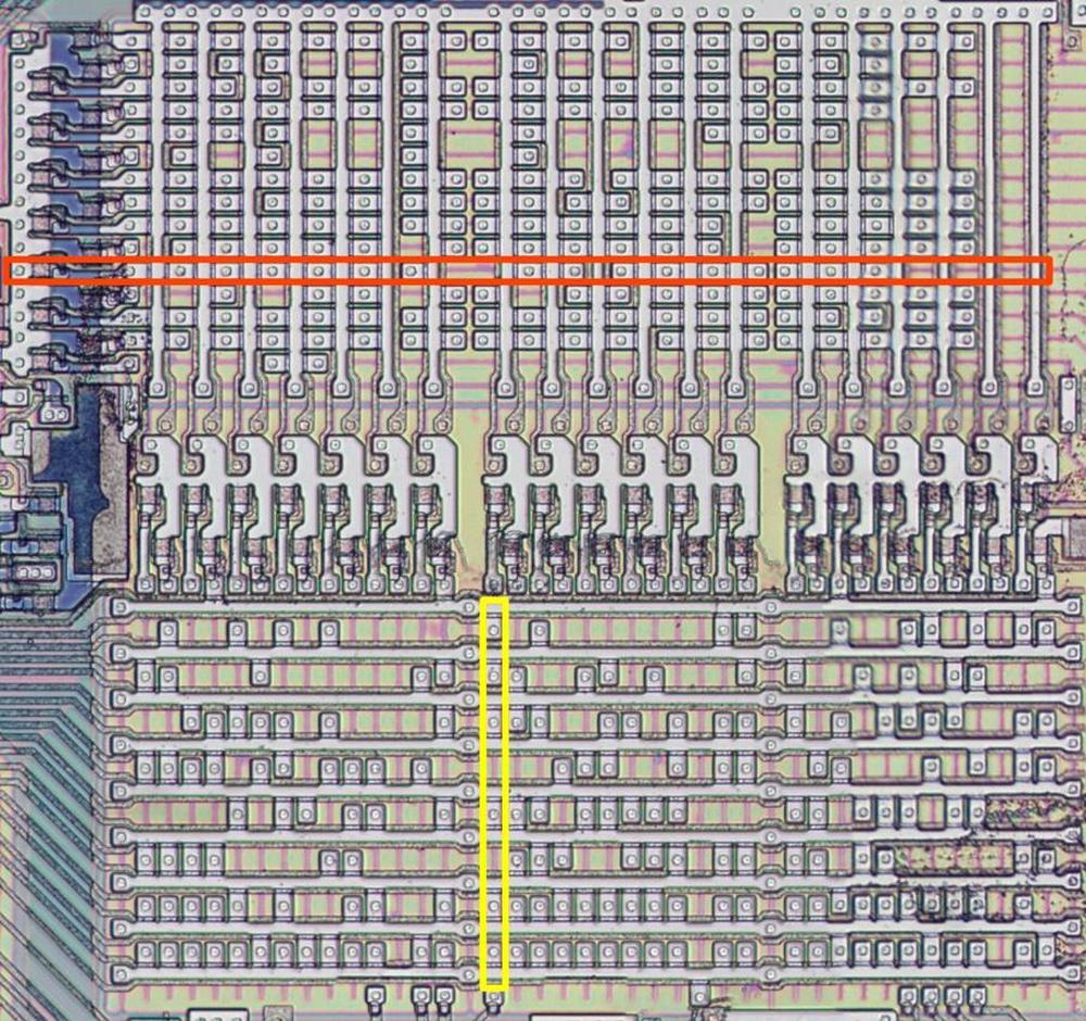
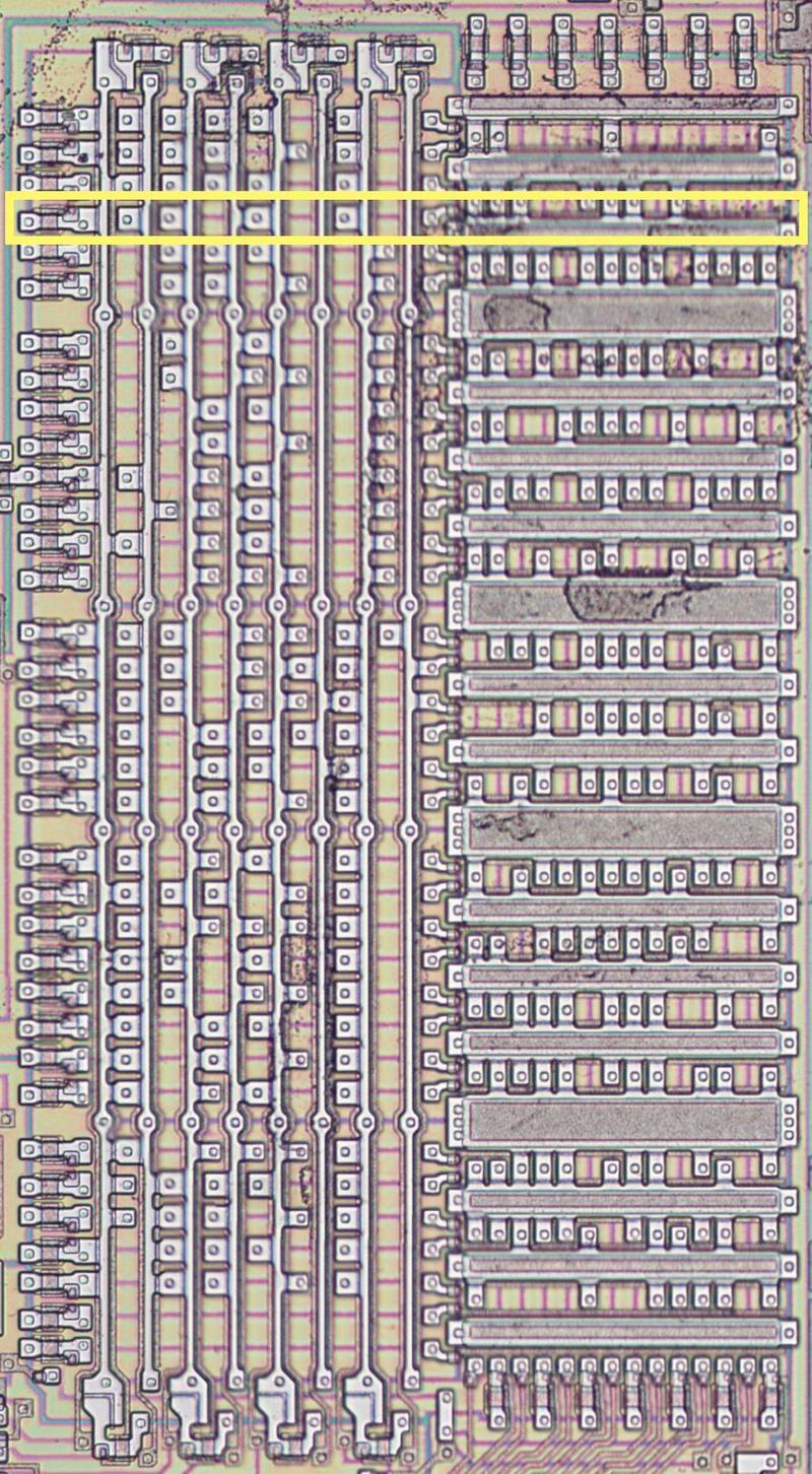
The Group Decode ROM. The yellow rectangle detects the HLT instruction, with an output at the bottom. The red rectangle generates the 1BL (one-byte logic) signal.

The Group Decode ROM. The yellow rectangle detects the HLT instruction, with an output at the bottom. The red rectangle generates the 1BL (one-byte logic) signal.

In the Execution Unit, the HALT signal blocks the reading of new instructions from the prefetch queue. This causes the loader to wait indefinitely and stops execution of new instructions. Since no new instruction replaces HLT, the Group Decode ROM continues to generate the HALT signal. The HALT signal also blocks most of the other outputs from the Group Decode ROM, preventing other decoding actions.

Thus, the Execution Unit sits idle as a result of the HLT instruction, unable to start a new instruction. Modern processors often have low-power halt modes, where part of the processor is shut down or a clock domain is stopped to reduce power consumption. The 8086, however, doesn't do anything clever to minimize power consumption in the halt mode, since this wasn't a concern for processors in the 1970s.

Halt processing in the Bus Interface Unit

Memory and I/O devices are connected to the 8086 chip through a bus that transmits address, data, and control information. The 8086's Bus Interface Unit handles reads and writes over this bus, running independently from the Execution Unit. A complete bus cycle for a read or write takes four clock periods, called T1, T2, T3, and T4,2 with specific signals on the bus for each time state.

A HLT instruction stops the Bus Interface Unit, but this takes several steps. First, the Bus Interface Unit must complete any currently-running bus cycle. Any new bus cycle must be blocked. Finally, the processor indicates the HALT state to any devices on the bus by issuing a special T1 cycle over the bus.

The main HALT control signal inside the Bus Interface Unit is something I call halt-not-hold, indicating a HALT is active, but not a HOLD. (Ignore the HOLD part for now.) This signal is activated by the HLT instruction signal from the Group Decode ROM, except it is blocked by any bus operations in progress. Once any current bus operation reaches T2, halt-not-hold gets activated and starts the halt process while the current bus cycle finishes up.

To prevent new bus activity, the halt-not-hold signal blocks new prefetch requests. The only other source of bus activity is an instruction that performs reads or writes. But the current instruction is HLT, so it won't generate any bus traffic. Thus, the Bus Interface Unit will remain idle.

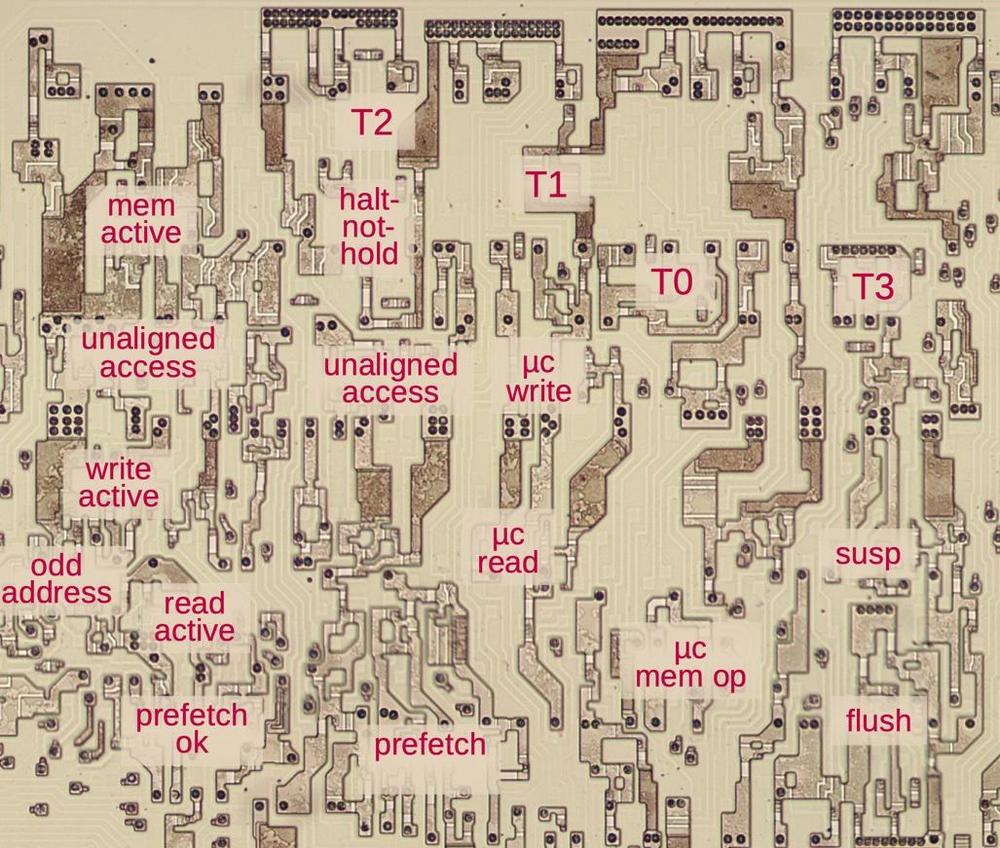
The read/write control circuitry on the die with the flip-flops labeled. Metal and polysilicon were removed to show the underlying silicon.

The read/write control circuitry on the die with the flip-flops labeled. Metal and polysilicon were removed to show the underlying silicon.

The circuitry to control the bus cycle is complicated with many flip-flops and logic gates; the diagram above shows the flip-flops. I plan to write about the bus cycle circuitry in detail later, but for now, I'll give an extremely simplified description. Internally, there is a T0 state before T1 to provide a cycle to set up the bus operation. The bus timing states are controlled by a chain of flip-flops configured like a shift register with additional logic: the output from the T0 flip-flop is connected to the input of the T1 flip-flop and likewise with T2 and T3, forming a chain. A bus cycle is started by putting a 1 into the input of the T0 flip-flop.3 When the CPU's clock transitions, the flip-flop latches this signal, indicating the (internal) T0 bus state. On the next clock cycle, this 1 signal goes from the T0 flip-flop to the T1 flip-flop, creating the externally-visible T1 state. Likewise, the signal passes to the T2 and T3 flip-flops in sequence, creating the bus cycle.

A slightly different path is used to generate the special T1 signal that indicates a HALT. Once any bus activity is completed, the halt-not-hold signal puts a 1 into the T1 flip-flop through some gates. This generates the T1 signal, bypassing T0. Moreover, this signal does not propagate to the T2 flip-flop because it is blocked by halt-not-hold and some gates. Another flip-flop blocks this T1 cycle after the first cycle so halt-not-hold doesn't repeately trigger it. Overall, this special HALT T1 state looks like a special case that was hacked into the circuitry.

One complication is the bus hold feature. The 8086 supports complex bus configurations, where external devices may take control of the bus. For instance, peripherals may use the bus for direct memory access, bypassing the CPU. A device can request control of the bus, a "bus hold", through the 8086's HOLD pin.4 This causes the 8086 to electrically stop putting signals on the bus (i.e. a high-impedance, tri-state off state). This allows another device to use the bus until it releases HOLD.

Even when the CPU is halted, the CPU still has "ownership" of the bus and drives the bus with idle signals.5 If a device requests a bus hold when the CPU is halted, the halt-not-hold signal is blocked. When the device releases the hold, halt-not-hold is unblocked. This causes the 8086 to go through the special T1 cycle again, using the same flip-flop process described above. This lets listeners on the bus know that the CPU is still halted.

Exiting the halt state

The processor exits the halt state when it receives a reset, interrupt, or non-maskable interrupt. To implement this, an interrupt unblocks the instruction decoder by overriding the queue-unavailable signal. This causes the loader, which controls instruction decoding, to move into the First Clock state. Meanwhile, the interrupt causes the microcode address register to be loaded with the hardcoded microcode address of the appropriate interrupt routine. Thus, the microcode engine starts running the interrupt handler microcode.

The Instruction Register holds the 8-bit opcode that is currently being processed. It has a ninth bit that indicates if an interrupt is being processed. The Instruction Register (including the interrupt bit) is loaded on First Clock (described above). It outputs the instruction and interrupt bit to the Group Decode ROM one clock cycle later. The interrupt bit blocks regular instruction decoding by the Group Decode ROM. In particular, the HLT instruction will no longer be decoded, dropping the HALT signal throughout the CPU. In the Execution Unit, this reactivates the prefetch queue. This will allow instruction execution once the microcode finishes executing the interrupt handling code. In the Bus Interface Unit, dropping the HALT signal causes halt-not-hold to drop. This enables bus activity from the Bus Interface Unit.6

History of HALT and x86

Historically, computers usually had some sort of "stop" or "wait" instruction to stop execution at the end of a program. This goes back to the electromechanical Harvard Mark I (1944), EDSCAC (1949), and Univac I (1951), among other machines. Most (but not all) mainframes and minicomputers continued this approach.7

The HLT instruction in the 8086, like many other features, derives from the Datapoint 2200, and there's an interesting story behind that. The Datapoint 2200 was a desktop computer announced in 1970, and sold as a "programmable terminal". The processor of the Datapoint 2200 was implemented with a board of TTL integrated circuits, since this was before microprocessors. The Datapoint manufacturer talked to Intel and Texas Instruments about replacing the board of chips with a single processor chip. Texas Instruments produced the TMX 1795 microprocessor chip and Intel produced the 8008 shortly after,8 both copying the Datapoint 2200's architecture and instruction set. Datapoint didn't like the performance of these chips and decided to stick with a TTL-based processor. Texas Instruments couldn't find a customer for the TMX 1795 and abandoned it. Intel, on the other hand, sold the 8008 as an 8-bit microprocessor, creating the microprocessor market in the process. Intel improved the 8008 to create the popular 8080 microprocessor (1974). Zilog produced the more powerful Z80 (1976), backward-compatible with the 8080.

The Datapoint 2200. This is the later Model II with an improved TTL processor using the 74181 ALU chip.

The Datapoint 2200. This is the later Model II with an improved TTL processor using the 74181 ALU chip.

Intel started designing the iAPX 432 in 1975 to be their high-end 32-bit processor, a "micromainframe" that supported garbage collection and objects in the processor. The iAPX 432 was too complex for the time and as the schedule slipped, Intel decided to produce a stopgap 16-bit processor to compete with Zilog and Motorola: this processor became the 8086. To make it easier for Intel customers to move to the 8086, the processor was designed for compatibility with 8080 assembly language so it inherited much of the architecture and instruction set, although extended from 8 bits to 16 bits.9

The consequence of this history is that the 8086 inherited many features from the Datapoint 2200. The Datapoint 2200 used cheaper shift-register memory so it had a serial processor that operated on one bit at a time. This required the Datapoint 2200 to be little-endian, a feature that lives on in the x86 architecture. Since the Datapoint 2200 was marketed as a programmable terminal, it had parity calculation built into the hardware. Thus, the 8008 and descendants have a parity flag, in contrast to contemporary processors such as the 6800 and 6502 that omitted this moderately complex feature. The use of I/O ports instead of memory-mapped I/O is another feature of the Datapoint 2200 that persists in the x86, but was not used in the 6800 and 6502 and their descendants. The opcodes of the Datapoint 2200 were based on octal 3-bit fields for hardware reasons. The x86 instructions are still designed around octal, but the usual hexadecimal display obscures their structure. Finally, the Datapoint 2200's HALT instruction was exactly copied by the 800810 and persists in x86.

Conclusions

The HLT instruction seems like a simple function, but its implementation touches many parts of the 8086. It is implemented in logic circuitry, completely bypassing the microcode. The implementation became more complicated because of the 8086's four-step bus protocol, as well as interaction between halting and the bus hold feature. This illustrates how complexity creates more complexity, something the RISC processors of the 1980s tried to counter.

I've written multiple posts on the 8086 so far and plan to continue reverse-engineering the 8086 die so follow me on Twitter @kenshirriff or RSS for updates. I've also started experimenting with Mastodon recently as @oldbytes.space@kenshirriff. Thanks to monocasa for suggesting this topic.

Notes and references

  1. The instructions implemented outside microcode are the segment register prefixes (ES:, CS:, SS:, DS:), the other prefixes (LOCK, REPNZ, REPZ), the simple flag instructions (CMC, CLC, STC, CLI, STI, CLD, STD), and HLT. These instructions are indicated by the 1BL (one-byte logic) output from the Group Decode ROM. 

  2. The bus cycle may also include optional Tw wait states after T3 for slow memory. The memory (or I/O device) lowers the READY pin until it is ready to proceed and the Bus Interface Unit waits. I'm ignoring Tw states in this discussion to keep things simpler. 

  3. For some reason, the T-state flip-flops all hold inverted signals, so strictly speaking a 0 bit goes through the flip-flops. 

  4. The 8086 has a separate prioritized "request/grant" way for a device to obtain a bus hold, but it doesn't change the underlying hold behavior. 

  5. During a HALT, the 8086 is not actively using the bus, but it does not release the bus either; it is still electrically driving the bus. Otherwise, the bus would float to random voltages, confusing attached memory chips or other circuitry. 

  6. When the Bus Interface Unit is unhalted due to an interrupt, you might expect it to immediately start prefetching, accessing unwanted instructions. It turns out that the prefetch circuitry does try to start prefetching and reaches the internal T0 bus state. But it then gets preempted by the interrupt handler microcode, which uses the bus to send two interrupt acknowledge cycles. Immediately after, the microcode routine suspends prefetching. Thus, prefetching doesn't run until the interrupt microcode finishes and reenables prefetching. There's a lot of tricky timing in the 8086 to make everything work. 

  7. For more history of the stop instruction, see "Computer Architecture", Blaauw and Brooks, page 349. (This the same Brooks who wrote "The Mythical Man-Month" and "No Silver Bullet".) 

  8. You might wonder how the Intel 4004 fits into this history. Although many of the same people worked on both chips, they have completely different architectures. The 8008 is not at all an 8-bit version of the 4-bit 4004. 

  9. Assembly code for the 8-bit 8080 processor couldn't run directly on the 16-bit 8086. Instead, a translation program converted the 8080 assembly language to be compatible with the 8086, making some changes in the process. The 8086 dropped some of the less-useful instructions of the 8080, replacing them with multiple instructions in the translation. For instance, the 8080 had conditional subroutine call and return instructions (inherited from the Datapoint 2200), but the 8086 dropped them. 

  10. To see that the 8008 copied the Datapoint 2200's HALT instruction, note that the Datapoint had three opcodes for HALT (00, 01, and FF), which is a bit unusual. The 8008 also has three opcodes for HLT: 00, 01, and FF. Most instructions in the 8008 used the same opcode values as the Datapoint, with a few minor changes. 

Reverse-engineering the conditional jump circuitry in the 8086 processor

Intel introduced the 8086 microprocessor in 1978 and it had a huge influence on computing. I'm reverse-engineering the 8086 by examining the circuitry on its silicon die and in this blog post I take a look at how conditional jumps are implemented. Conditional jumps are an important part of any instruction set, changing the flow of execution based on a condition. Although this instruction may seem simple, it involves many parts of the CPU: the 8086 uses microcode along with special-purpose condition logic.

The die photo below shows the 8086 microprocessor under a microscope. The metal layer on top of the chip is visible, with the silicon and polysilicon mostly hidden underneath. Around the edges of the die, bond wires connect pads to the chip's 40 external pins. I've labeled the key functional blocks; the ones that are important to this discussion are darker and will be discussed in detail below. Architecturally, the chip is partitioned into a Bus Interface Unit (BIU) at the top and an Execution Unit (EU) below. The BIU handles memory accesses, while the Execution Unit (EU) executes instructions. Most of the relevant circuitry is in the Execution Unit, such as the condition evaluation circuitry near the center, and the microcode in the lower right. But the Bus Interface Unit plays a part too, holding and modifying the program counter.

The 8086 die under a microscope, with main functional blocks labeled. This photo shows the chip's single metal layer; the polysilicon and silicon are underneath. Click on this image (or any other) for a larger version.

The 8086 die under a microscope, with main functional blocks labeled. This photo shows the chip's single metal layer; the polysilicon and silicon are underneath. Click on this image (or any other) for a larger version.

Microcode

Most people think of machine instructions as the basic steps that a computer performs. However, many processors (including the 8086) have another layer of software underneath: microcode. One of the hardest parts of computer design is creating the control logic that directs the processor for each step of an instruction. The straightforward approach is to build a circuit from flip-flops and gates that moves through the various steps and generates the control signals. However, this circuitry is complicated, error-prone, and hard to design.

The alternative is microcode: instead of building the control circuitry from complex logic gates, the control logic is largely replaced with code. To execute a machine instruction, the computer internally executes several simpler micro-instructions, specified by the microcode. In other words, microcode forms another layer between the machine instructions and the hardware. The main advantage of microcode is that it turns design of control circuitry into a programming task instead of a difficult logic design task.

The 8086 uses a hybrid approach: although the 8086 uses microcode, much of the instruction functionality is implemented with gate logic. This approach removed duplication from the microcode and kept the microcode small enough for 1978 technology. In a sense, the microcode is parameterized. For instance, the microcode can specify a generic Arithmetic/Logic Unit (ALU) operation, and the gate logic determines from the instruction which ALU (Arithmetic/Logic Unit) operation to perform. More relevant to this blog post, the microcode can specify a generic conditional test and the gate logic determines which condition to use. Although this made the 8086's gate logic more complicated, the tradeoff was worthwhile.

Microcode for conditional jumps

The 8086 processor has six status flags: carry, parity, auxiliary carry, zero, sign, and overflow.1 These flags are updated by arithmetic and logic operations based on the result. The 8086 has sixteen different conditional jump instructions2 that test status flags and jump if conditions are satisfied, such as zero, less than, or odd parity. These instructions are very important since they permit if statements, loops, comparisons, and so forth.

In machine language, a conditional jump opcode is followed by a signed offset byte which specifies a location relative to the current program counter, from 127 bytes ahead to 128 bytes back. This is a fairly small range, but the benefit is that the offset fits in a single byte, reducing the code size.3 For typical applications such as loops or conditional code, jumps usually stay in the same neighborhood of code, so the tradeoff is worthwhile.

The 8086's microcode was disassembled by Andrew Jenner (link) from my die photos, so we can see exactly what micro-instructions the 8086 is running for each machine instruction. The microcode below implements conditional jumps. In brief, the conditional jump code (Jcond) gets the branch offset byte. It tests the appropriate condition and, if satisfied, jumps to the relative jump microcode (RELJUMP). The RELJMP code adds the offset to the program counter. In either case, the microcode routine ends when it runs the next instruction (RNI).

   move       action
Jcond:
1 Q→tmpBL
2          XC    RELJMP                    
3          RNI                       

RELJMP:
4          SUSP
5          CORR                      
6 PC→tmpA  ADD   tmpA
7 Σ→PC     FLUSH RNI                       

In more detail, micro-instruction 1 (arbitrary numbering) moves a byte from the prefetch queue (Q) across the queue bus to the ALU's temporary B register.4 (Arguments for ALU operations are first stored in temporary registers, invisible to the programmer.) Instruction 2 tests the appropriate condition with XC, and jumps to the RELJMP routine if the condition is satisfied.5 Otherwise, RNI (Run Next Instruction) ends this sequence and loads the next machine instruction without jumping.

If the condition is satisfied, the relative jump routine starts with instruction 4, which suspends prefetching.6 Instruction 5 corrects the program counter value, since it normally points to the next byte to prefetch, not the next byte to execute. Instruction 6 moves the corrected program counter address to the ALU's temporary A register. It also starts an ALU operation to add temporary A and temporary B. Instruction 7 moves the sum (Σ) to the program counter. It flushes the prefetch queue, which starts up prefetching from the new PC value. Finally, RNI runs the next instruction, from the updated address.

This code supports all 16 conditional jumps because the microcode tests the generic "XC" condition. This indicates that the specific test depends on the four low bits of the opcode, and the hardware determines exactly what to test. It's important to keep the two levels straight: the machine instruction is doing a conditional jump to a different memory address, while the microcode that implements this instruction is performing a conditional jump to a different micro-address.

The timing for conditional jumps

The RNI (Run Next Instruction) micro-operation initiates processing of the next machine instruction. However, it takes a clock cycle to get the next instruction from the prefetch queue, decode it, and start the appropriate micro-instruction. This causes a wasted clock cycle before the next micro-instruction executes. To avoid this delay, most microcode routines issue a NXT micro-operation one cycle before they end. This gives the 8086 time to decode the next machine instruction so micro-instructions can run uninterrupted.

Unfortunately, the conditional jump instructions can't take advantage of NXT. The problem is that the control flow in the microcode depends on whether the conditional jump is taken or not. By the time the microcode knows it is not taking the branch, it's too late to issue NXT.

The datasheet gives the timing of a conditional jump as 4 clock cycles if the jump is not taken, and 8 clock cycles if the jump is taken. Looking at the microcode explains these timings. There are 3 micro-instructions executed if the jump is not taken, and 7 if it is taken. Because of the RNI, there is one wasted clock cycle, resulting in the documented 4 or 8 cycles in total.

The conditions

At this point I will review the 8086's conditional jumps. The 8086 implements 16 conditional jumps. (This is a large number compared to earlier CPUs: the 8080, 6502, and Z80 all had 8 conditional jumps, specified by 3 bits.) The table below shows which flags are tested for each condition, specified by the low four bits of the opcode. Some jump instructions have multiple names depending on the programmer's interpretation, but they map to the same machine instruction.7

ConditionBitsCondition trueCondition false
Overflow Flag (OF)=1000xoverflow (JO)not overflow (JNO)
Carry Flag (CF)=1001xcarry (JC)
below (JB)
not above or equal (JNAE)
not carry (JNC)
not below (JNB)
above or equal (JAE)
Zero Flag (ZF)=1010xzero (JZ)
equal (JE)
not zero (JNZ)
not equal (JNE)
CF=1 or ZF=1011xbelow or equal (JBE)
not above (JNA)
not below or equal (JNBE)
above (JA)
Sign Flag (SF)=1100xsign (JS)not sign (JNS)
Parity Flag (PF)=1101xparity (JP)
parity even (JPE)
not parity (JNP)
parity odd (JPO)
SF ≠ OF110xless (JL)
not greater or equal (JNGE)
not less (JNL)
greater or equal (JGE)
ZF=1 or SF ≠ OF111xless or equal (JLE)
not greater (JNG)
not less or equal (JNLE)
greater (JG)

From the hardware perspective, the important thing is that there are eight different condition flag tests. Each test has two jump instructions associated with it: one that jumps if the condition is true, and one that jumps if the condition is false. The low bit of the opcode selects "if true" or "if false".

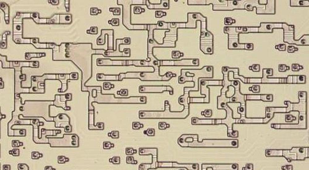
The image below shows the condition evaluation circuitry as it appears on the die. There isn't much structure to it; it's just a bunch of gates. This image shows the doped silicon regions that form transistors. The numerous small polygons with a circle inside are connections between the metal layer and the polysilicon layer. Many of these connections use the silicon layer to optimize the layout.

The circuitry to compute conditions as it appears on the die. The metal and polysilicon layers have been removed for this image, showing the silicon underneath.

The circuitry to compute conditions as it appears on the die. The metal and polysilicon layers have been removed for this image, showing the silicon underneath.

This circuitry evaluates each condition by getting the instruction bits from the Instruction Register, checking the bits to match each condition, and testing if the condition is satisfied. For instance, the overflow condition (with instruction bits 000x) is computed by a NOR gate: NOR(IR3, IR2, IR1, OF'), which will be true if instruction register bits 3, 2, and 1 are zero and the Overflow Flag is 1.

The results from the individual condition tests are combined with a 7-input NOR gate, producing a result that is 0 if the specified 3-bit condition is satisfied. Finally, the "if true" and "if false" cases are handled by flipping this signal depending on the low bit of the instruction. This final result indicates if the 4-bit condition in the instruction is satisfied, and this signal is passed on to the microcode control circuitry.

One unexpected feature of the implementation is that a 7-input NOR gate combines the various conditions to test if the selected condition is satisfied. You'd expect that with eight conditions, there would be eight inputs to the NOR gate. However, there is a clever optimization that takes advantage of conditions that are combinations of clauses, for example, "less or equal". Specifically, the zero flag is tested for bit pattern 01xx (where x indicates a 0 or 1), which covers two conditions with one gate. Likewise, SF≠OF is tested for bit pattern 11xx and CF=1 is tested for bit pattern 0x1x. With these optimizations, the eight conditions are covered with seven checks. (This shows that the opcodes weren't assigned arbitrarily: the bit patterns needed to be carefully assigned for this to work.)

Back to the microcode

Before explaining how the microcode jump circuitry works, I'll briefly discuss the microcode format. A micro-instruction is encoded into 21 bits as shown below. Every micro-instruction contains a move from a source register to a destination register, each specified with 5 bits. The meaning of the remaining bits is a bit tricky since it depends on the type field, which is two or three bits long. The "short jump" (type 0) is a conditional jump within the current block of 16 micro-instructions. The ALU operation (type 1) sets up the arithmetic-logic unit to perform an operation. Bookkeeping operations (type 4) are anything from flushing the prefetch queue to ending the current instruction. A memory read or write is type 6. A "long jump" (type 5) is a conditional jump to any of 16 fixed microcode locations (specified in an external table). Finally, a "long call" (type 7) is a conditional subroutine call to one of 16 locations (different from the jump targets).

The encoding of a micro-instruction into 21 bits. Based on NEC v. Intel: Will Hardware Be Drawn into the Black Hole of Copyright?

The encoding of a micro-instruction into 21 bits. Based on NEC v. Intel: Will Hardware Be Drawn into the Black Hole of Copyright?

I'm going to focus on the XC RELJMP micro-instruction that we saw in the microcode earlier. This is a "long jump" with XC as the condition and RELJMP as the target tag. Another layer of hardware is required to implement the microcode conditions. The microcode supports 16 conditions, which are completely different from the 16 programmer-level conditions.8 Some microcode conditions test special-purpose internal flags, while others test conditions such as an interrupt, the chip's TEST pin, bit 3 of the opcode, or if the instruction has a one-byte address offset. The XC condition is one of these 16 conditions, number 15 specifically.

The conditions are evaluated by the condition PLA (Programmable Logic Array, a grid of gates), shown below. The four condition bits from the micro-instruction, along with their complements, are fed into the columns. The PLA has 16 rows, one for each condition. Each row is a NOR gate matching one bit combination (i.e. selecting a condition) and the corresponding signal value to test.9 Thus, if a particular condition is specified and is satisfied, that row will be 1. The 16 row outputs are combined by the 16-input NOR gate at the left. Thus, if the specified condition is satisfied, this output will be 0, and if the condition is unsatisfied, the output will be 1. This signal controls the jump or call micro-instruction: if the condition is satisfied, the new micro-address is loaded into the microcode address register. If the condition is not satisfied, the microcode proceeds sequentially.

The condition PLA evaluates microcode conditionals.

The condition PLA evaluates microcode conditionals.

Conclusions

To summarize, the 8086 processor implements 16 conditional jump instructions. One piece of microcode efficiently implements all 16 instructions, with gate logic determining which flags to test, depending on bits in the machine instruction. The result of this test is used by the microcode XC conditional jump, one of 16 completely different microcode-level conditions. If the XC condition is satisfied, the program counter is updated by adding the offset, jumping to the new location.

Conditional jumps are relatively straightforward instructions from the programmer's perspective, but they interact with most parts of the 8086 processor including the prefetch queue, the address adder, the ALU, microcode, and the Translation ROM. The diagram below shows the interactions for each step of the jump.

The conditional jump involves many parts of the die, shown in this diagram.

The conditional jump involves many parts of the die, shown in this diagram.

I've written multiple posts on the 8086 so far and plan to continue reverse-engineering the 8086 die so follow me on Twitter @kenshirriff or RSS for updates. I've also started experimenting with Mastodon recently as @oldbytes.space@kenshirriff.

Notes and references

  1. In addition to the six status flags, the 8086 has three control flags: trap, direction, and interrupt enable. These flags aren't tested by conditional branches so I won't discuss them further. 

  2. Strictly speaking, the 8086 has a few more conditional jumps. The JCXZ instruction tests if the CX register is zero. The LOOP, LOOPNZ, and LOOPZ instructions decrement the CX register and loop if it is nonzero. The last two only loop if the zero flag indicates nonzero or zero, respectively. I'm ignoring these instructions in the blog post. 

  3. Although a conditional jump only supports a small range, it's still possible to conditionally jump to a distant location by using two instructions. A conditional jump with the opposite condition can skip over a longer unconditional jump instruction. The 80386 removed this restriction by providing long-displacement conditional jumps, which could perform a 16-bit or 32-bit relative jump. 

  4. The relative offset byte is sign-extended when it is moved to the temporary B register. That is, if the top bit is high, the high byte is set to all 1's to produce a 16-bit negative value. 

  5. The details of how the microcode jumps to the RELJMP routine are interesting, but a bit of a tangent, so I've put this discussion in a footnote. For long jumps (and long calls) in microcode, the target micro-addresses are stored in the Translation ROM, and the 4-bit target tag indexes into this ROM. The motivation for this structure is that micro-addresses are 13 bits, which is a lot of bits to try to fit into a 21-bit micro-instruction. Using a 4-bit tag keeps the microcode compact, but at the cost of requiring a small ROM in the 8086.

    The translation ROM on the die.

    The translation ROM on the die.

    Above is a view of the Translation ROM, with the RELJMP entry highlighted. The left half decodes tags, while the right half provides the corresponding microcode address. The row for RELJMP is highlighted. 

  6. Much of this microcode snippet deals with the prefetch queue. To increase efficiency, the 8086 processor fetches instructions from memory before they are needed and stores them in a 6-byte prefetch queue. In most processors, the program counter points to the memory address of the next instruction to execute. However, in the 8086, the program counter advances during prefetching, so it points to the memory address of the next instruction to fetch. This discrepancy is invisible to the programmer, but the microcode needs to handle it.

    First, the microcode issues a SUSP micro-operation to suspend prefetching. This ensures that the program counter will not be changed due to more prefetching. Next, the CORR micro-operation corrects the program counter to point to the next address to execute. This correction is performed by subtracting the number of unused bytes in the prefetch queue. You might expect this correction to be performed by the Arithmetic/Logic Unit (ALU). However, the 8086 has a separate adder that is used for memory address computations: each memory access in the 8086 requires a segment register base address to be added to an offset address. This address adder is also used for program counter correction. The constant ROM holds the values -1 through -6, the appropriate constant is selected based on the number of bytes in the prefetch queue, and this constant is added to the program counter. (Interestingly, the address adder is used for program counter correction, while the ALU is used to modify the program counter for the relative jump computation.)

    The address adder has multiple uses. It is also used for updating the program counter during prefetching. It updates addresses when performing block copy operations. Finally, it updates addresses when performing an unaligned word operation. The constant ROM holds constants for these operations.

    At the end of the microcode sequence, the FLUSH micro-operation flushes the stale bytes from the prefetch queue, resets the prefetch queue pointers, and restarts prefetching. I wrote about prefetching in detail here

  7. Often, the compare (CMP) instruction will be executed to compare two numbers by subtracting and discarding the result but keeping the condition codes. One complication is that some tests make sense for signed numbers, while other tests make sense for unsigned numbers. Specifically, "greater", "greater or equal", "less", and "less or equal" make sense for signed comparisons. On the other hand, "above", "above or equal", "below", and "below or equal" make sense for unsigned comparisons.

    The 8086 supports both signed and unsigned numbers. The arithmetic operations are the same for both; it's just the programmer's interpretation that differs. For instance, consider adding hex numbers 0xfe and 0x01. Treating them as unsigned numbers, the sum is 254 + 1 = 255. But as signed numbers, -2 + 1 = -1. In either case, the processor computes the same result, 0xff, but the interpretation is different.

    The signed vs unsigned distinction matters for comparisons. For instance, as unsigned numbers, 0xfe (254) is above 0x01 (1). But as signed numbers, 0xfe (-2) is less than 0x01 (1). This is why different instructions are used to compare unsigned versus signed numbers.

    Another important factor is that the carry flag indicates an unsigned result is too large for its byte (or word), while the overflow flag indicates that a signed result is too large for its byte (or word). For instance, adding unsigned bytes 0xff (255) and 0x02 (2) yields 0x01 (1) and a carry, indicating the result is too big for a byte. However, as signed bytes this corresponds to -1 + 2 = 1, which fits in a byte, so the overflow flag is not set. Conversely, 0x7f + 0x01 = 0x80. As unsigned bytes, this corresponds to 127 + 1 = 128 which is fine. But as signed bytes, this corresponds to 127 + 1, which unexpectedly yields -128 due to overflow. Thus, the carry flag is not set, but the overflow flag is set in this case. 

  8. Short jumps have four bits to specify the condition, so they can access 16 conditions. For long jumps and long calls, one bit is "stolen" from the condition to indicate the type, so they can only access eight of the conditions. Thus, the conditions need to be assigned carefully so the necessary ones are available. 

  9. PLAs are typically uniform grids, but the grid pattern breaks down a bit in the condition PLA. The reason is that each test uses a separate signal, so there is a different signal into each row (unlike a typical PLA where each row receives the same signals). Moreover, some of the test signals are processed at the left, distorting the 16-input NOR gate. This illustrates the degree of layout optimization in the 8086, squeezing transistors in to save a bit of space.