Inside the Globus INK: a mechanical navigation computer for Soviet spaceflight

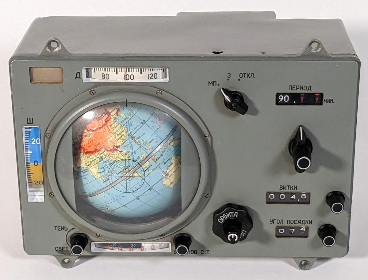
The Soviet space program used completely different controls and instruments from American spacecraft. One of the most interesting navigation instruments onboard Soyuz spacecraft was the Globus, which used a rotating globe to indicate the spacecraft's position above the Earth. This navigation instrument was an electromechanical analog computer that used an elaborate system of gears, cams, and differentials to compute the spacecraft's position. Officially, the unit was called a "space navigation indicator" with the Russian acronym ИНК (INK),1 but I'll use the more descriptive nickname "Globus".

The INK-2S "Globus" space navigation indicator. Coincidentally, the latitude indicator matches the Ukrainian flag.

The INK-2S "Globus" space navigation indicator. Coincidentally, the latitude indicator matches the Ukrainian flag.

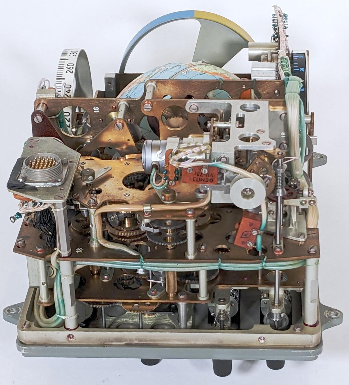
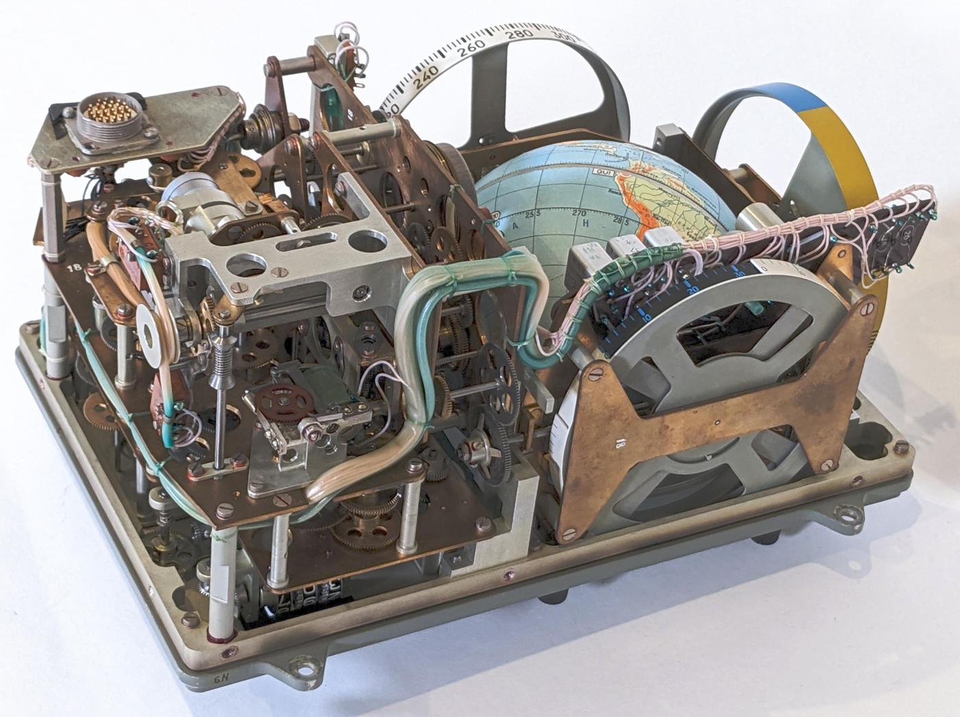
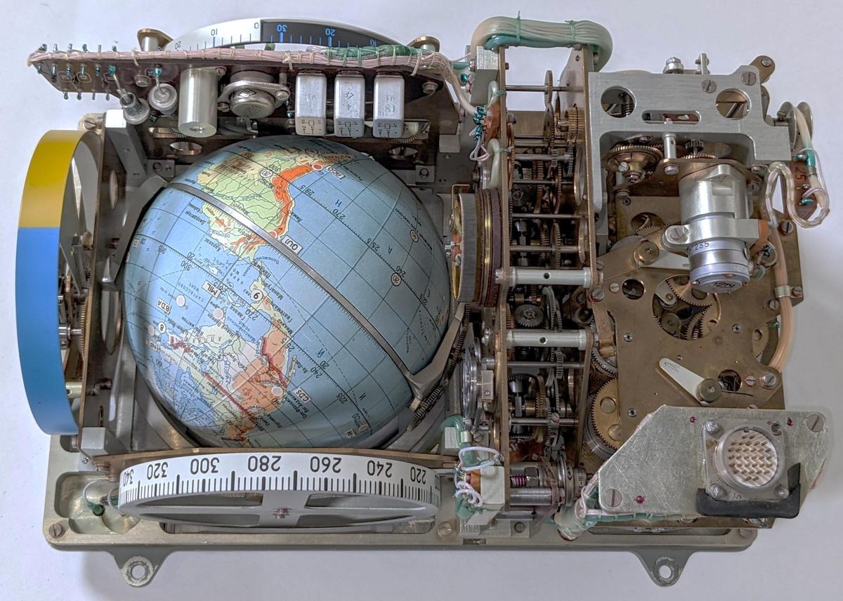
We recently received a Globus from a collector and opened it up for repair and reverse engineering. In this blog post, I explain how it operated, show its internal mechanisms, and describe what I've learned so far from reverse engineering. The photo below gives an idea of the mechanical complexity of this device, which also has a few relays, solenoids, and other electrical components.

Side view of the Globus INK. Click this (or any other image) for a larger version.

Side view of the Globus INK. Click this (or any other image) for a larger version.

Functionality

The primary purpose of the Globus was to indicate the spacecraft's position. The globe rotated while fixed crosshairs on the plastic dome indicated the spacecraft's position. Thus, the globe matched the cosmonauts' view of the Earth, allowing them to confirm their location. Latitude and longitude dials next to the globe provided a numerical indication of location. Meanwhile, a light/shadow dial at the bottom showed when the spacecraft would be illuminated by the sun or in shadow, important information for docking. The Globus also had an orbit counter, indicating the number of orbits.

The Globus had a second mode, indicating where the spacecraft would land if they fired the retrorockets to initiate a landing. Flipping a switch caused the globe to rotate until the landing position was under the crosshairs and the cosmonauts could evaluate the suitability of this landing site.

The cosmonauts configured the Globus by turning knobs to set the spacecraft's initial position and orbital period. From there, the Globus electromechanically tracked the orbit. Unlike the Apollo Guidance Computer, the Globus did not receive navigational information from an inertial measurement unit (IMU) or other sources, so it did not know the spacecraft's real position. It was purely a display of the predicted position.

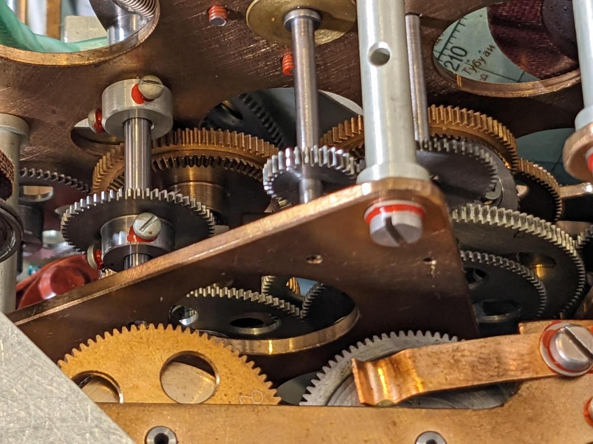
A close-up of the complex gear trains in the Globus.

A close-up of the complex gear trains in the Globus.

The globe

The globe itself is detailed for its small size, showing terrain features such as mountains, lakes, and rivers. These features on the map helped cosmonauts compare their position with the geographic features they could see on Earth. These features were also important for selecting a landing site, so they could see what kind of terrain they would be landing on. For the most part, the map doesn't show political boundaries, except for thick red and purple lines. This line shows the borders of the USSR, as well as the boundaries between communist and non-communist countries, also important for selecting a landing site. The globe also has numbered circles 1 through 8 that indicate radio sites for communication with the spacecraft, allowing the cosmonauts to determine what ground stations could be contacted.

A view of the globe showing Asia.

A view of the globe showing Asia.

Controlling the globe

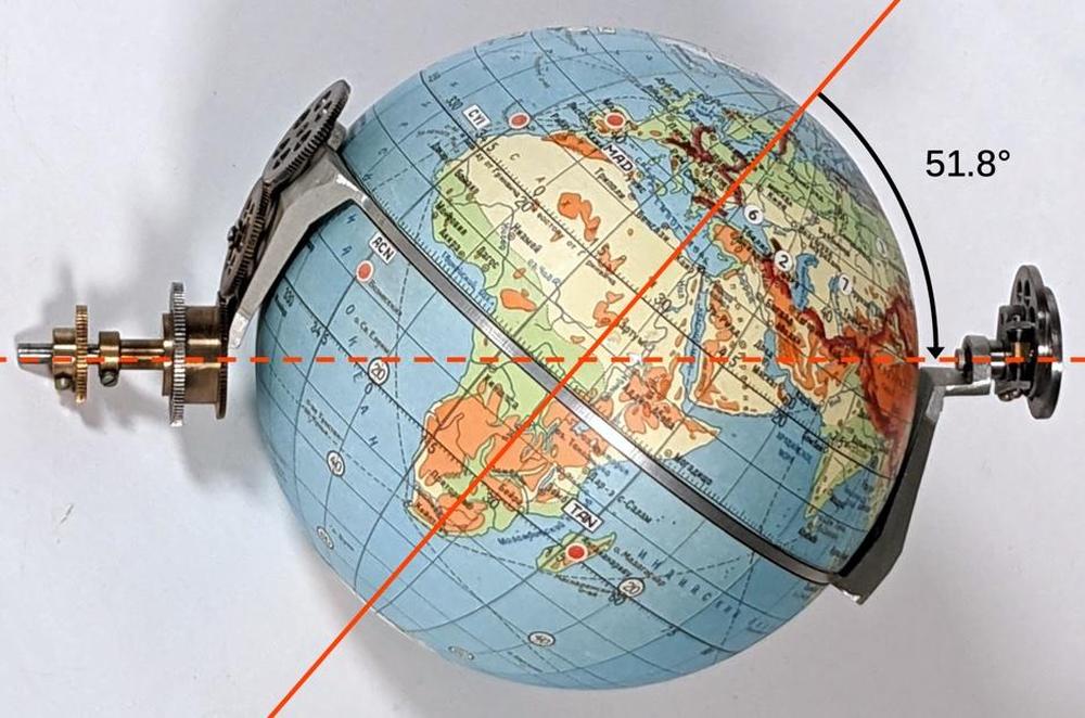
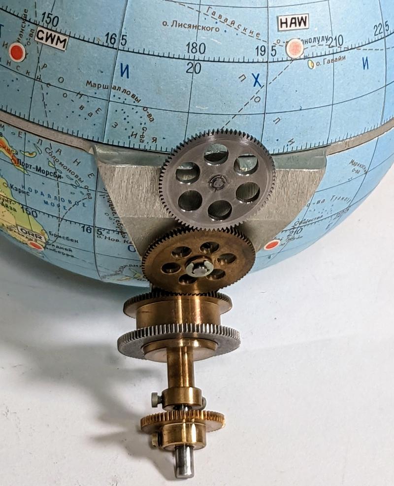
On seeing the Globus, one might wonder how the globe is rotated. It may seem that the globe must be free-floating so it can rotate in two axes. Instead, a clever mechanism attaches the globe to the unit. The key is that the globe's equator is a solid piece of metal that rotates around the horizontal axis of the unit. A second gear mechanism inside the globe rotates the globe around the North-South axis. The two rotations are controlled by concentric shafts that are fixed to the unit, allowing two rotational degrees of freedom through fixed shafts.

The photo below shows the frame that holds and controls the globe. The dotted axis is fixed horizontally in the unit and rotations are fed through the two gears at the left. One gear rotates the globe and frame around the dotted axis, while the gear train causes the globe to rotate around the vertical polar axis (while the equator remains fixed).

The axis of the globe is at 51.8° to support that orbital inclination.

The axis of the globe is at 51.8° to support that orbital inclination.

The angle above is 51.8° which is very important: this is the inclination of the standard Soyuz orbit. As a result, simply rotating the globe around the dotted line causes the crosshair to trace the standard orbit.2 Rotating the two halves of the globe around the poles yields the different 51.8° orbits over the Earth's surface as the Earth rotates. (Why 51.8 degrees? The Baikonur Cosmodrome, launching point for Soyuz, is at 45.97° N latitude, so 45.97° would be the most efficient inclination. However, to prevent the launch from passing over western China, the rocket must be angled towards the north, resulting in 51.8° (details).)

One important consequence of this design is that the orbital inclination is fixed by the angle of the globe mechanism. Different Globus units needed to be built for different orbits. Moreover, this design only handles circular orbits, making it useless during orbit changes such as rendezvous and docking. These were such significant limitations that some cosmonauts wanted the Globus removed from the control panel, but it remained until it was replaced by a computer display in Soyuz-TMA (2002).3

A closeup of the gears that drive the motion of the two halves of the globe around the polar axis, leaving the equator fixed.

A closeup of the gears that drive the motion of the two halves of the globe around the polar axis, leaving the equator fixed.

This Globus had clearly suffered some damage. The back of the case had some large dents.7 More importantly, the globe's shaft had been knocked loose from its proper position and no longer meshed with the gears. This also put a gouge into Africa, where the globe hit internal components. Fortunately, CuriousMarc was able to get the globe back into position while ensuring that the gears had the right timing. (Putting the globe back arbitrarily would mess up the latitude and longitude.)

Orbital speed and the "cone"

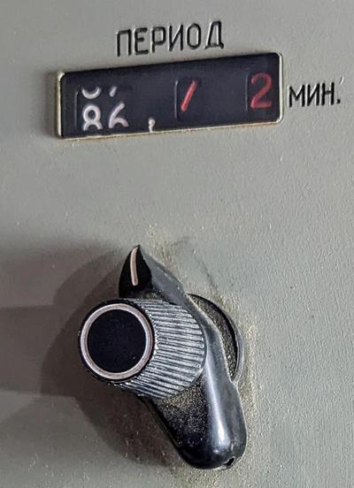
An orbit of Soyuz takes approximately 90 minutes, but the time varies according to altitude.4 The Globus has an adjustment knob (below) to adjust the orbital period in minutes, tenths of minutes, and hundredths of minutes. The outer knob has three positions and points to the digit that changes when the inner knob is turned. The mechanism provides an adjustment of ±5 minutes from the nominal period of 91.85 minutes.3

The control to adjust the orbital period.

The control to adjust the orbital period.

The orbital speed feature is implemented by increasing or decreasing the speed at which the globe rotates around the orbital (horizontal) axis. Generating a variable speed is tricky, since the Globus runs on fixed 1-hertz pulses. The solution is to start with a base speed, and then add three increments: one for the minutes setting, one for the tenths-of-minutes setting, and one for the hundredths-of-minutes setting.5 These four speeds are added (as shaft rotation speeds) using obtain the overall rotation speed.

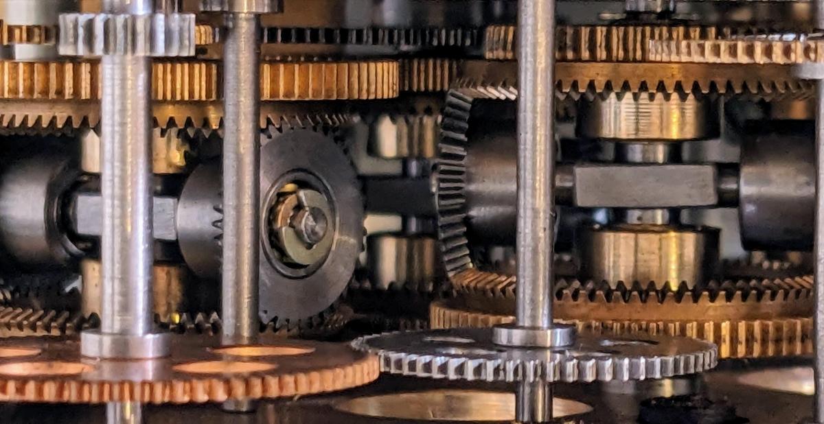
The Globus uses numerous differential gears to add or subtract rotations. The photo below shows two sets of differential gears, side-by-side.

Two differential gears in the Globus.

Two differential gears in the Globus.

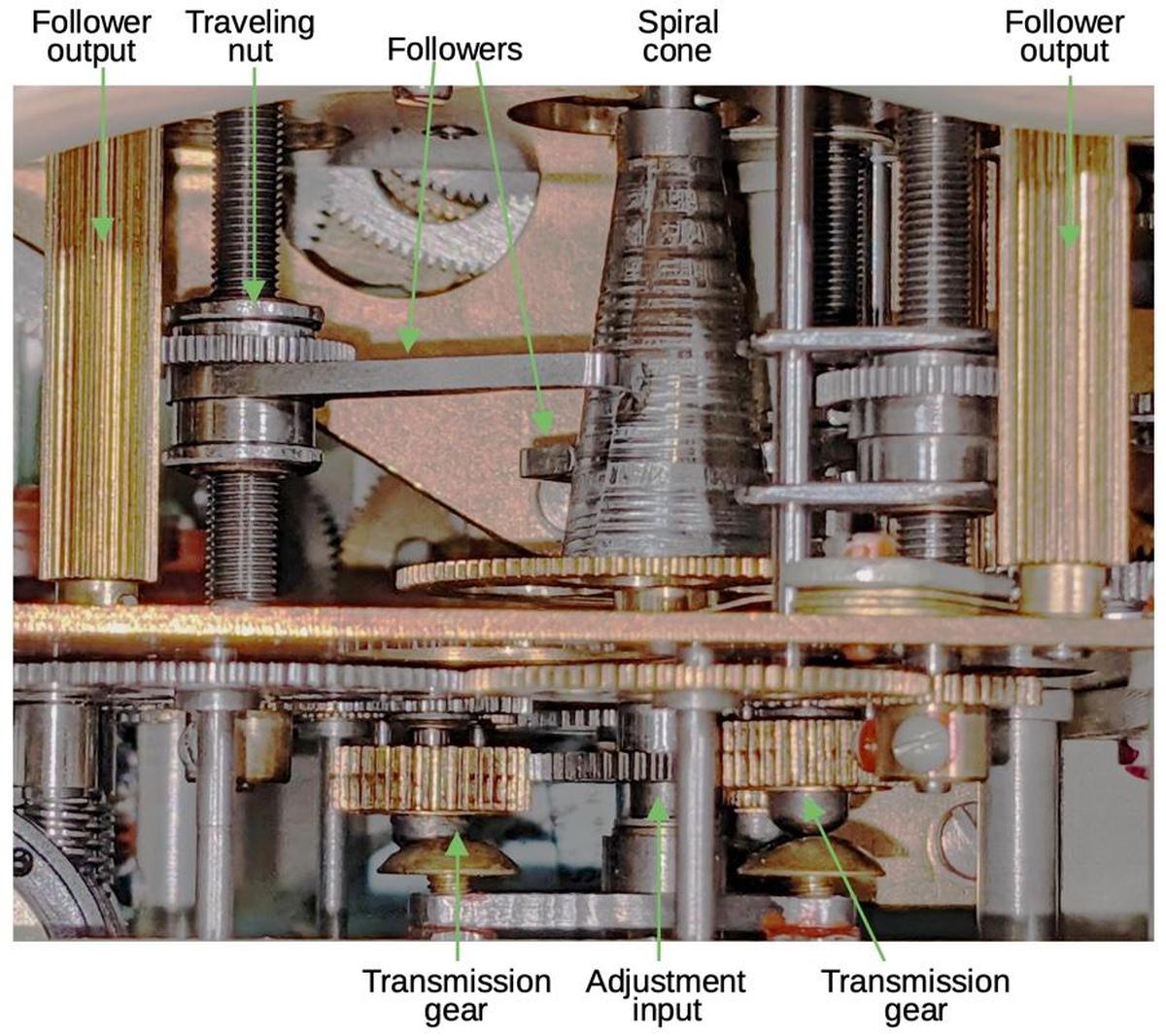
The problem is how to generate these three variable rotation speeds from the fixed input. The solution is a special cam, shaped like a cone with a spiral cross-section. Three followers ride on the cam, so as the cam rotates, the follower is pushed outward and rotates on its shaft. If the follower is near the narrow part of the cam, it moves over a small distance and has a small rotation. But if the follower is near the wide part of the cam, it moves a larger distance and has a larger rotation. Thus, by moving the follower to a particular point on the cam, the rotational speed of the follower is selected.

A diagram showing the orbital speed control mechanism. The cone has three followers, but only two are visible from this angle. The "transmission" gears are moved in and out by the outer knob to select which follower is adjusted by the inner knob.

A diagram showing the orbital speed control mechanism. The cone has three followers, but only two are visible from this angle. The "transmission" gears are moved in and out by the outer knob to select which follower is adjusted by the inner knob.

Obviously, the cam can't spiral out forever. Instead, at the end of one revolution, its cross-section drops back sharply to the starting diameter. This causes the follower to snap back to its original position. To prevent this from jerking the globe backward, the follower is connected to the differential gearing via a slip clutch and ratchet. Thus, when the follower snaps back, the ratchet holds the drive shaft stationary. The drive shaft then continues its rotation as the follower starts cycling out again. Thus, the output is a (mostly) smooth rotation at a speed that depends on the position of the follower.

Latitude and longitude

The indicators at the left and the top of the globe indicate the spacecraft's latitude and longitude respectively. These are defined by surprisingly complex functions, generated by the orbit's projection onto the globe.6

The latitude and longitude functions are implemented through the shape of metal cams; the photo below shows the longitude mechanism. Each function has two cams: one cam implements the desired function, while the other cam has the "opposite" shape to maintain tension on the jaw-like tracking mechanism.

The cam mechanism to compute longitude.

The cam mechanism to compute longitude.

The latitude cam drives the latitude dial, causing it to oscillate between 51.8° N and 51.8° S. Longitude is more complicated because the Earth's rotation causes it to constantly vary. The longitude output on the dial is produced by adding the cam's value to the Earth's rotation through a differential gear.

Light and shadow

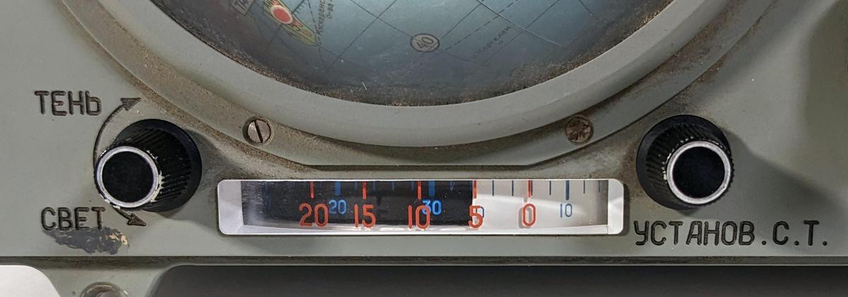
The Globus has an indicator to show when the spacecraft will enter light or shadow. The dial consists of two concentric dials, configured by the two knobs. These dials move with the spacecraft's orbit, while the red legend remains fixed. I think these dials are geared to the longitude dial, but I'm still investigating.

The light and shadow indicator is controlled by two knobs.

The light and shadow indicator is controlled by two knobs.

The landing location mechanism

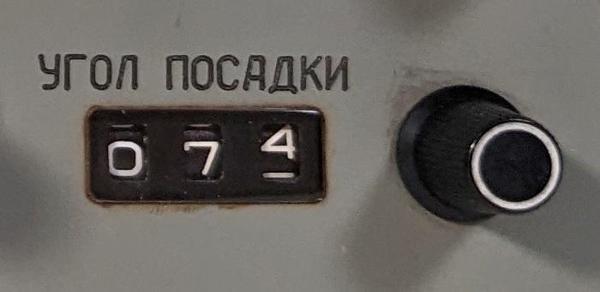
The Globus can display where the spacecraft would land if you started a re-entry burn now, with an accuracy of 150 km. This is computed by projecting the current orbit forward by a partial orbit, depending on how long it would take to land. The cosmonaut specifies this value by the "landing angle", which indicates this fraction of an orbit as an angle. An electroluminescent indicator in the upper-left corner of the unit shows "Место посадки" (Landing place) to indicate this mode.

The landing angle control.

The landing angle control.

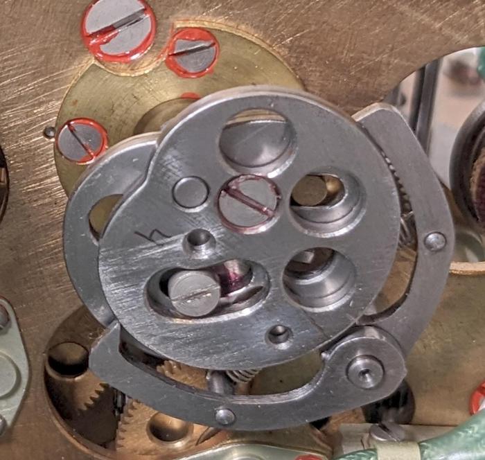
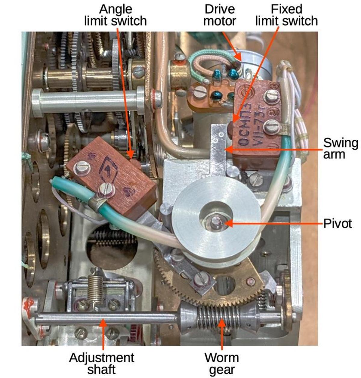
To obtain the landing position, a motor spins the globe until it is stopped after rotating through the specified angle. The mechanism to implement this is shown below. The adjustment knob on the panel turns the adjustment shaft which moves the limit switch to the desired angle via the worm gear. The wiring is wrapped around a wheel so the wiring stays controlled during this movement. When the drive motor is activated, it rotates the globe and the swing arm at the same time. Since the motor stops when the swing arm hits the angle limit switch, the globe rotates through the desired angle. The fixed limit switch is used when returning the globe's position to its regular, orbital position.

The landing angle function uses a complex mechanism.

The landing angle function uses a complex mechanism.

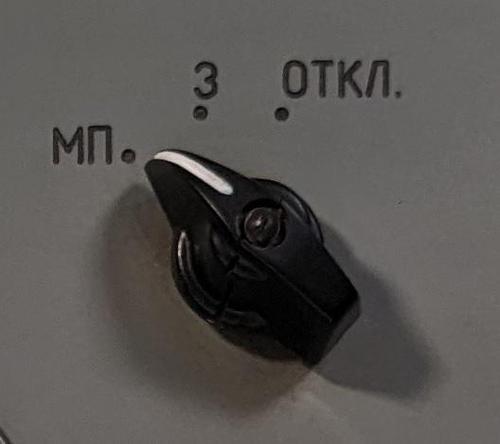
The landing location mode is activated by a three-position rotary switch. The first position "МП" (место посадки, landing site) selects the landing site, the second position "З" (Земля, Earth) shows the position over the Earth, and the third position "Откл" (off) undoes the landing angle rotation and turns off the mechanism.

The rotary switch to select the landing angle mode.

The rotary switch to select the landing angle mode.

Electronics

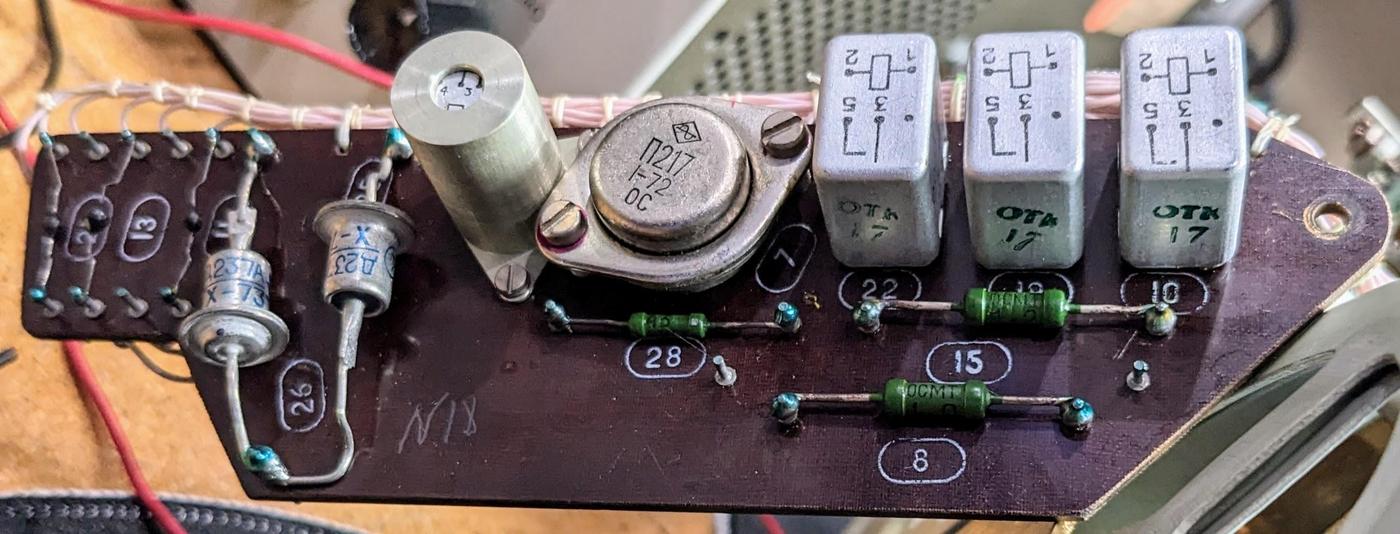
Although the Globus is mostly mechanical, it has an electronics board with four relays and a transistor, as well as resistors and diodes. I think that most of these relays control the landing location mechanism, driving the motor forward or backward and stopping at the limit switch. The diodes are flyback diodes, two diodes in series across each relay coil to eliminate the inductive kick when the coil is disconnected.

The electronics circuit board.

The electronics circuit board.

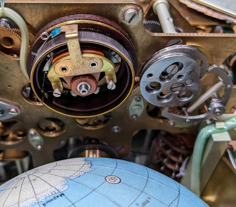
A 360° potentiometer (below) converts the spacecraft's orbital position into a voltage. Sources indicate that the Globus provides this voltage signal to other units on the spacecraft. My theory is that the transistor on the electronics board amplifies this voltage, but I am still investigating.

The potentiometer converts the orbital position into a voltage.
To the right is the cam that produces the longitude display. Antarctica is visible on the globe.

The potentiometer converts the orbital position into a voltage. To the right is the cam that produces the longitude display. Antarctica is visible on the globe.

The photo below shows the multiple wiring bundles in the Globus, at the front and the left. The electronics board is at the front right. The Globus contains a surprising amount of wiring for a device that is mostly mechanical. Inconveniently, all the wires to the box's external connector (upper left) were cut.7 Perhaps this was part of decommissioning the unit. However, one of the screws on the case is covered with a tamper-resistant wax seal with insignia, and this wax seal was intact. This indicates that the unit was officially re-sealed after cutting the wires, which doesn't make sense for a decommissioned unit.

This view shows the back and underside of the Globus. The round connector at the back left provided the interface with the rest of the spacecraft. The black wires under this connector were all cut.

This view shows the back and underside of the Globus. The round connector at the back left provided the interface with the rest of the spacecraft. The black wires under this connector were all cut.

The drive solenoids

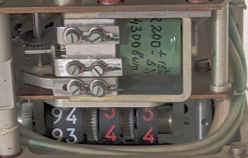
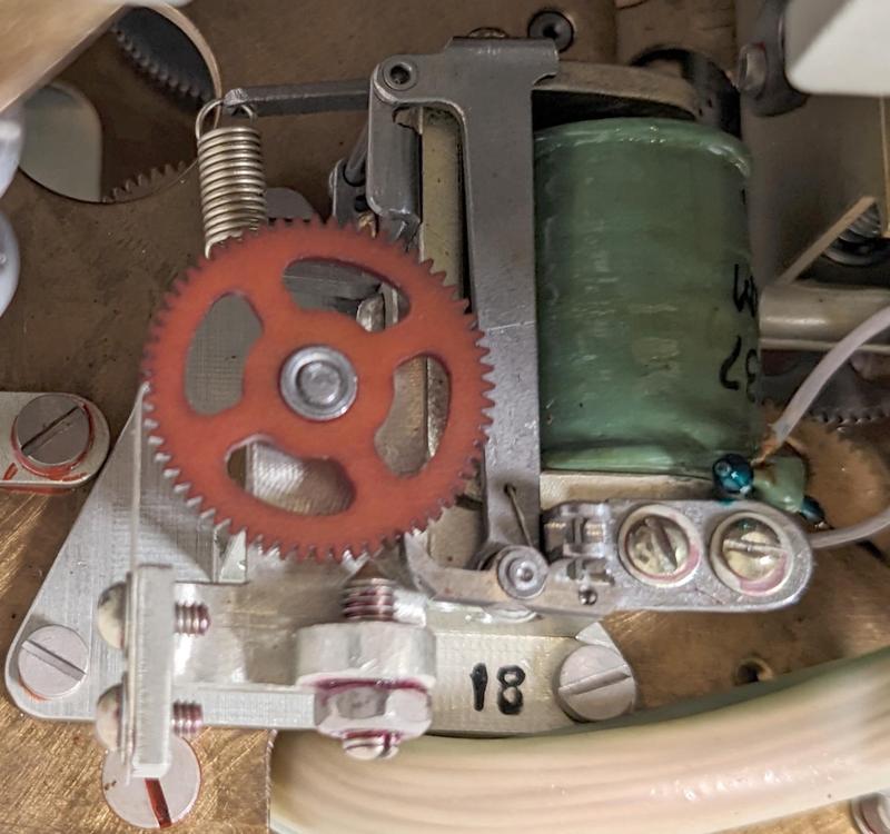
The unit is driven by two ratchet solenoids: one for the orbital rotation and one for the Earth's rotation. These solenoids take 27-volt pulses at 1 hertz.3 Each pulse causes the solenoid to advance the gear by one tooth; a pawl keeps the gear from slipping back. These small rotations drive the gears throughout the Globus and result in a tiny movement of the globe.

One of the driving solenoids in the Globus. The wheels to indicate orbital time are underneath.

One of the driving solenoids in the Globus. The wheels to indicate orbital time are underneath.

The other driving solenoid in the Globus.

The other driving solenoid in the Globus.

Apollo-Soyuz

If you look closely at the globe, it has a bunch of pink dots added, along with three-letter labels in Latin (not Cyrillic) characters.8 In the photo below, you can see GDS (Goldstone), MIL (Merritt Island), BDA (Bermuda), and NFL (Newfoundland). These are NASA tracking sites, which implies that this Globus was built for the Apollo-Soyuz Test Project, a 1975 mission where an Apollo spacecraft docked with a Soyuz capsule.

North America as it appears on the globe. The US border is marked in red. The selection of cities seems a bit random, such as El Paso as the only western city until the coast.

North America as it appears on the globe. The US border is marked in red. The selection of cities seems a bit random, such as El Paso as the only western city until the coast.

Further confirmation of the Apollo-Soyuz connection is the VAN sticker in the middle of the Pacific Ocean (not visible above). The USNS Vanguard was a NASA tracking ship that was used in the Apollo program to fill in gaps in radio coverage. It was an oil tanker from World War II, converted postwar to a missile tracking ship and then used for Apollo. In the photo below, you can see the large tracking antennas on its deck. During the Apollo-Soyuz mission, Vanguard was stationed at 25 S 155 W for the Apollo-Soyuz mission, exactly matching the location of the VAN dot on the globe.

The USNS Vanguard with a NASA C-54 plane overhead. (source).

The USNS Vanguard with a NASA C-54 plane overhead. (source).

History

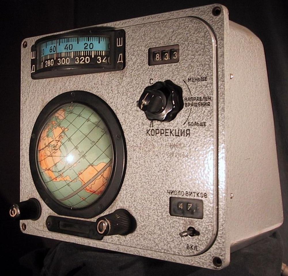
The Globus has a long history, back to the beginnings of Soviet crewed spaceflight. The first version was simpler and had the Russian acronym ИМП (IMP).9 Development of the IMP started in 1960 for the Vostok (1961) and Voshod (1964) spaceflights.

The Globus IMP. Photo from Francoisguay (CC BY-SA 3.0).

The Globus IMP. Photo from Francoisguay (CC BY-SA 3.0).

The basic functions of the earlier Globus IMP are similar to the INK, showing the spacecraft's position and the landing position. It has an orbit counter in the lower right. The latitude and longitude displays at the top were added for the Voshod flights. The large correction knob allows the orbital period to be adjusted. The main differences are that the IMP doesn't have a display at the bottom for sun and shade and doesn't have a control to set the landing angle.9 Unlike the INK, the mode (orbit vs landing position) was selected by external switches, rather than a switch on the unit.

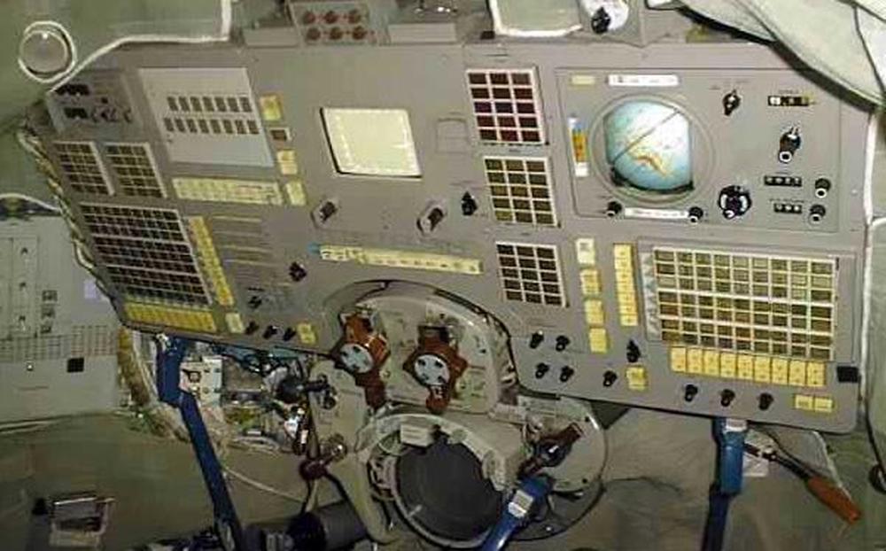
The more complex INK model (described in this blog post) was created for the Soyuz flights, starting in 1967. It was part of the "Sirius" information display system (IDS). The Neptun IDS used on Soyuz-T (1976) and the Neptun-M for Soyuz-TM (1986) modernized much of the console but kept the Globus INK. The photo below shows the Globus mounted in the upper-right of a Soyuz-TM console.

The Neptun-M IDS for the Soyuz-TM (source).

The Neptun-M IDS for the Soyuz-TM (source).

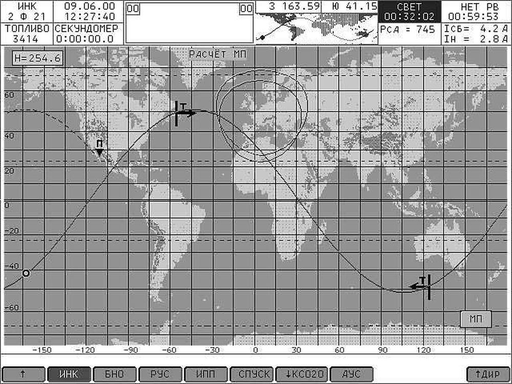
The Soyuz-TMA (2002) upgraded to the Neptun-ME system3 which used digital display screens. In particular, the Globus was replaced with the graphical display below.

A computer display from the Neptune-ME display system used in the Soyuz-TMA spaceship. The Soyuz consoles are much simpler than the Apollo or Space Shuttle consoles, and built with completely different design principles. From Information Display Systems for Soyuz Spaceships.

A computer display from the Neptune-ME display system used in the Soyuz-TMA spaceship. The Soyuz consoles are much simpler than the Apollo or Space Shuttle consoles, and built with completely different design principles. From Information Display Systems for Soyuz Spaceships.

Conclusions

The Globus INK is a remarkable piece of machinery, an analog computer that calculates orbits through an intricate system of gears, cams, and differentials. It provided cosmonauts with a high-resolution, full-color display of the spacecraft's position, way beyond what an electronic space computer could provide in the 1960s.

Although the Globus is an amazing piece of mechanical computation, its functionality is limited. Its parameters must be manually configured: the spacecraft's starting position, the orbital speed, the light/shadow regions, and the landing angle. It doesn't take any external guidance inputs, such as an IMU (inertial measurement unit), so it's not particularly accurate. Finally, it only supports a circular orbit at a fixed angle. While the more modern digital display lacks the physical charm of a rotating globe, the digital solution provides much more capability.

I plan to continue reverse-engineering the Globus and hope to get it operational, so follow me on Twitter @kenshirriff or RSS for updates. I've also started experimenting with Mastodon recently as @oldbytes.space@kenshirriff. Many thanks to Marcel for providing the Globus. Thanks to Stack Overflow for orbit information and my Twitter followers for translation assistance.

I should give a disclaimer that I am still reverse-engineering the Globus, so what I described is subject to change. Also, I don't read Russian, so any errors are the fault of Google Translate. :-)

With the case removed, the complex internals of the Globus are visible.

With the case removed, the complex internals of the Globus are visible.

Notes and references

  1. In Russian, the name for the device is "Индикатор Навигационный Космический" abbreviated as ИНК (INK). This translates to "space navigation indicator." The name Globus (Глобус) seems to be a nickname, and I suspect it's more commonly used in English than Russian. 

  2. To see how the angle between the poles and the globe's rotation results in the desired orbital inclination, consider two limit cases. First, suppose the angle between is 90°. In this case, the globe is "straight" with the equator horizontal. Rotating the globe along the horizontal axis, flipping the poles end-over-end, will cause the crosshair to trace a polar orbit, giving the expected inclination of 90°. On the other hand, suppose the angle is 0°. In this case, the globe is "sideways" with the equator vertical. Rotating the globe will cause the crosshair to remain over the equator, corresponding to an equatorial orbit with 0° inclination. 

  3. A detailed description of Globus in Russian is in this document, in Section 5. 

  4. Or conversely, the altitude varies according to the speed. 

  5. Note that panel control adjusts the period of the orbit, while the implementation adjusts the speed of the orbit. These are reciprocals, so linear changes in the period result in hyperbolic changes in the speed. The mechanism, however, changes the speed linearly, which seems like it wouldn't work. However, since the period is large relative to the change in the period, this linear approximation works and the error is small, about 1%. It's possible that the cone has a nonlinear shape to correct this, but I couldn't detect any nonlinearity in photographs. 

  6. The latitude is given by arcsin(sin i * sin (2πt/T)), while the longitude is given by λ = arctan (cos i * tan(2πt/T)) + Ωt + λ0, where t is the spaceship's flight time starting at the equator, i is the angle of inclination (51.8°), T is the orbital period, Ω is the angular velocity of the Earth's rotation, and λ0 is the longitude of the ascending node.3

    The formula for latitude is simpler than longitude because the latitude repeats every orbit. The longitude, however, continually changes as the Earth rotates under the spacecraft. 

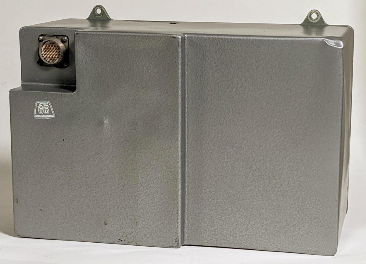
  7. The back of the Globus has a 32-pin connector, a standard RS32TV Soviet military design. The case also has some dents visible; the dents were much larger before CuriousMarc smoothed them out.

    The back of the Globus.

    The back of the Globus.


  8. The NASA tracking sites marked with dots are CYI (Grand Canary Island), ACN (Ascension), MAD (Madrid, Spain), TAN (Tananarive, Madagascar), GWM (Guam), ORR (Orroral, Australia), HAW (Hawaii), GDS (Goldstone, California), MIL (Merritt Island, Florida), QUI (Quito, Ecuador), AGO (Santiago, Chile), BDA (Bermuda), NFL (Newfoundland, Canada), and VAN (Vanguard tracking ship). Most of these sites were part of the Spacecraft Tracking and Data Network. The numbers 1-7 are apparently USSR communication sites, although I'm puzzled by 8 in Nova Scotia and 9 in Honduras. 

  9. Details on the earlier Globus IMP are at this site, including a discussion of the four different versions IMP-1 through IMP-4. Wikipedia also has information. 

Counting the transistors in the 8086 processor: it's harder than you might think

How many transistors are in Intel's 8086 processor? This seems like a straightforward question, but it doesn't have a straightforward answer. Most sources say that this processor has 29,000 transistors.1 However, I have traced out every transistor from die photos and my count is 19,618. What accounts for the 9382 missing transistors?

The explanation is that when manufacturers report the transistor count of chips, typically often report "potential" transistors. Chips that include a ROM will have different numbers of transistors depending on the values stored in the ROM. Since marketing doesn't want to publish varying numbers depending on the number of 1 bits and 0 bits, they often count ROM sites: places that could have transistors, but might not. A PLA (Programmable Logic Array) has similar issues; the transistor count depends on the desired logic functions.

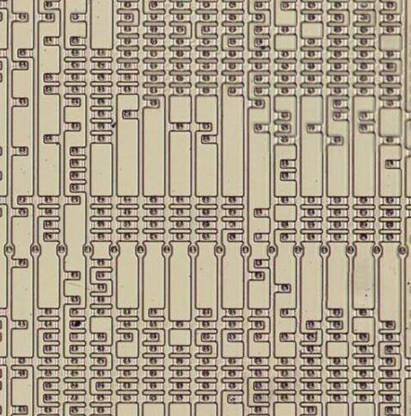
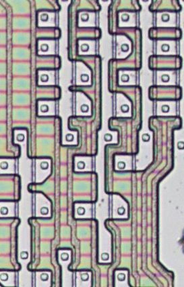
What are these potential transistor sites? ROMs are typically constructed as a grid of cells, with a transistor at a cell for a 1 bit, and no transistor for a 0 bit.2 In the 8086, transistors are created or not through the pattern of silicon doping. The photo below shows a closeup of the silicon layer for part of the 8086's microcode ROM. The empty regions are undoped silicon, while the other regions are doped silicon. Transistor gates are formed where vertical polysilicon lines (removed for the photo) passed over the doped silicon. Thus, depending on the data encoded into the ROM during manufacturing, the number of transistors varies.

A closeup of part of the microcode ROM. The dark circles indicate vias between the silicon and the metal on top.

A closeup of part of the microcode ROM. The dark circles indicate vias between the silicon and the metal on top.

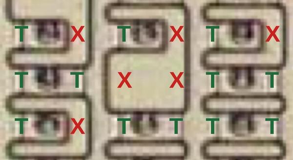
The diagram below provides more detail, showing the microcode ROM up close. Green T's indicate transistors, while red X's indicate positions with no transistor. As you can see, the potential transistor positions form a grid, but only some of the positions are occupied by transistors. The common method for counting transistors counts all the potential positions (18 below) rather than the actual transistors that are implemented (12 below).

An extreme closeup of the microcode ROM. Green T's indicate transistors, while red X's indicate positions with no transistor.

An extreme closeup of the microcode ROM. Green T's indicate transistors, while red X's indicate positions with no transistor.

I found an Intel history that confirmed that the 8086 transistor count includes potential sites, saying "This is 29,000 transistors if all ROM and PLA available placement sites are counted." That paper gives the approximate number of (physical) transistors in the 8086 as 20,000. This number is close to my count of 19,618.

To get a transistor count that includes empty sites, I counted the number of transistor sites in the various ROMs and PLAs in the 8086 chip. This is harder than you might expect because the smaller ROMs, such as the constant ROM, have some layout optimization. The photo below shows a closeup of the constant ROM. It is essentially a grid, but has been "squeezed" slightly to optimize its layout, making it slightly irregular. I'm counting its "potential" transistors, but one could argue that it shouldn't be counted because filling in these transistors might run into problems.

Closeup of the constant ROM showing the silicon and polysilicon.

Closeup of the constant ROM showing the silicon and polysilicon.

The following table breaks down the ROM and PLA counts by subcomponent. I found a total of approximately 9659 unfilled transistor vacancies. If you add those to my transistor count, it works out to 29,277 transistors.

ComponentTransistor sitesTransistorsVacancies
Microcode1390462107694
Group Decode ROM1254603651
Translation ROM1050431619
Register PLAs465182283
ALU PLA354170184
Constant ROM20310994
Condition PLA1607486
Segment PLA904248

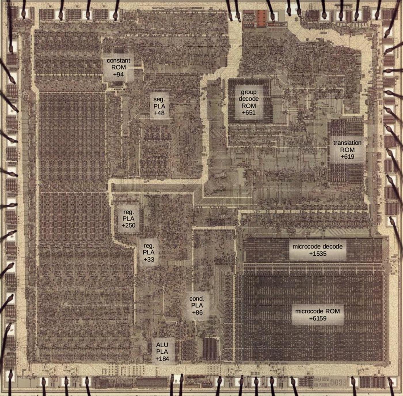
The image below shows these ROMs and PLAs on the die and how much the vacancies increase the transistor count. Not surprisingly, the large microcode ROM and its decoding PLA are responsible for most of the vacancies.

The 8086 die with transistor vacancy counts and how much they contribute to the final transistor count. (Click this image or any other for a larger version.)

The 8086 die with transistor vacancy counts and how much they contribute to the final transistor count. (Click this image or any other for a larger version.)

Potential exclusions

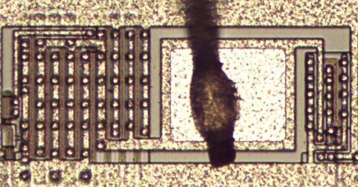
So are my counts of 19,618 transistors and 29,277 transistor sites correct? There are some subtleties that could lower this count slightly. First, the output pins use large, high-current transistors. Each output transistor is constructed from more than a dozen transistors wired in parallel. Should this be counted as a dozen transistors or a single transistor? I'm counting the component transistors.

An output pad with a bond wire attached. Driver transistors next to the pad are constructed from multiple transistors in parallel.

An output pad with a bond wire attached. Driver transistors next to the pad are constructed from multiple transistors in parallel.

The 8086 has about 43 transistors wired as diodes for various purposes. Some are input protection diodes, while others are used in the charge pump for the substrate bias generator. Should these be excluded from the transistor count? Physically they are transistors but functionally they aren't.

The 8086 is built with NMOS logic which builds gates out of active "enhancement" transistors as well as "depletion" transistors which basically act as pull-up resistors. I count 2689 depletion-mode transistors, but you could exclude them from the count as not "real" transistors.

Conclusions

The number of transistors in a chip is harder to define than you might expect. The 8086 is commonly described as having 29,000 transistors when including empty sites in ROMs and PLAs that potentially could have a transistor. The published number of physical transistors in the 8086 is "approximately 20,000". From my counts, the 8086 has 19,618 physical transistors and 29,277 transistors when including empty sites. Given the potential uncertainties in counting, it's not surprising that Intel rounded the numbers to the nearest thousand.

The practice of counting empty transistor sites may seem like an exaggeration of the real transistor count, but there are some good reasons to count this way. Including empty sites gives a better measure of the size and complexity of the chip, since these sites take up area whether or not they are used. This number also lets one count the number of transistors before the microcode is written, and it is also stable as the microcode changes. But when looking at transistor counts, it's good to know exactly what is getting counted.

I plan to continue reverse-engineering the 8086 die so follow me on Twitter @kenshirriff or RSS for updates. I've also started experimenting with Mastodon recently as @oldbytes.space@kenshirriff. I discussed the transistor count in the 6502 processor here.

Notes and references

  1. For example, The 8086 Family Users Manual says on page A-210: "The central processor for the iSBC 86/12 board is Intel's 8086, a powerful 16-bit H-MOS device. The 225 sq. mil chip contains 29,000 transistors and has a clock rate of 5MHz." 

  2. ROMs can also be constructed the other way around, with a transistor indicating a 0. It's essentially an arbitrary decision, depending on whether the output buffer inverts the bit or not. Other ROM technologies may have transistors at all the sites but only connect the desired ones. 

Reverse-engineering an airspeed/Mach indicator from 1977

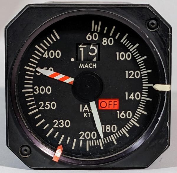
How does a vintage airspeed indicator work? CuriousMarc picked one up for a project, but it didn't have any documentation, so I reverse-engineered it. This indicator was used in the cockpit panel for business jets such as the Gulfstream G-III, Cessna Citation, and Bombardier Challenger CL600. It was probably manufactured in 1977 based on the dates on its transistors.

You might expect that the indicators on an aircraft control panel are simple dials. But behind this dial is a large, 2.8-pound box with a complex system of motors, gears, and feedback potentiometers, controlled by two boards of electronics. But for all this complexity, the indicator doesn't have any smarts: the pointers just indicate voltages fed into it from an air data computer. This is a quick blog post to summarize what I found.

Front view of the indicator.

Front view of the indicator.

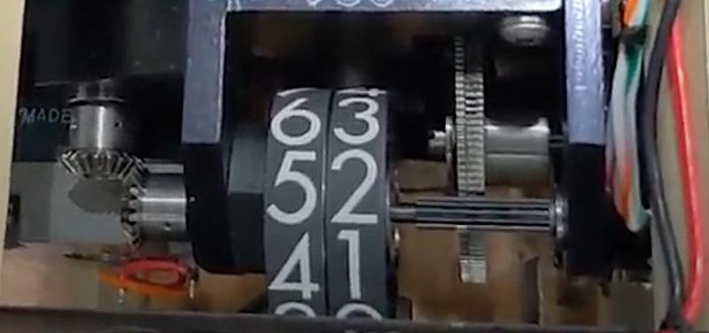
The dial has two rotating pointers: the white pointer indicates airspeed in knots while the striped pointer indicates the maximum airspeed (which varies depending on altitude). The "digital" indicator at the top shows Mach number from 0.10 to 0.99, implemented with rotating digit wheels. When the unit is operating, the OFF indicator flag switches to black. The flag switches to a bright VMO warning if the pilot exceeds the maximum airspeed.1 On the rim of the dial, two small markers called "bugs" can be manually moved to indicate critical speeds such as takeoff speed.

In use, the indicator is connected to a Sperry air data computer and receives voltage signals to control the dial positions.3 The air data computer measures the static and dynamic air pressure from pitot tubes and determines the airspeed, Mach number, altitude, and other parameters. (These calculations become nontrival near Mach 1 as air compresses and the fluid dynamics change.) Since we didn't have the air data computer or its specifications, I needed to figure out the connections from the computer to the display.

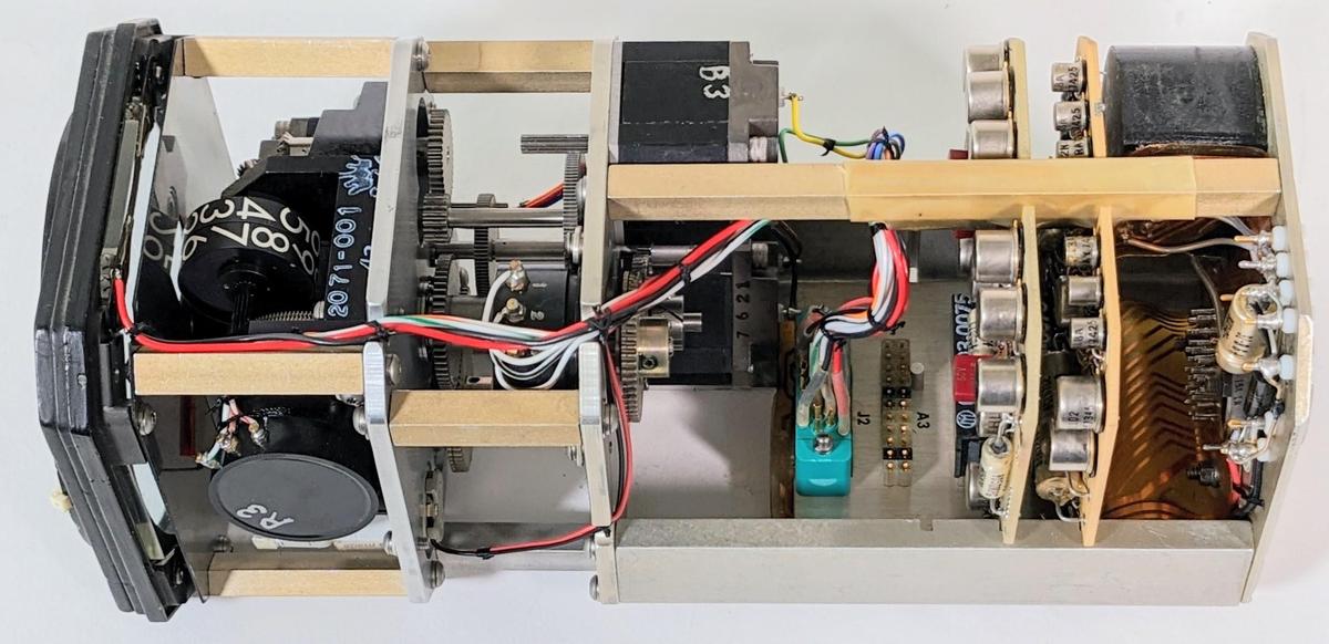
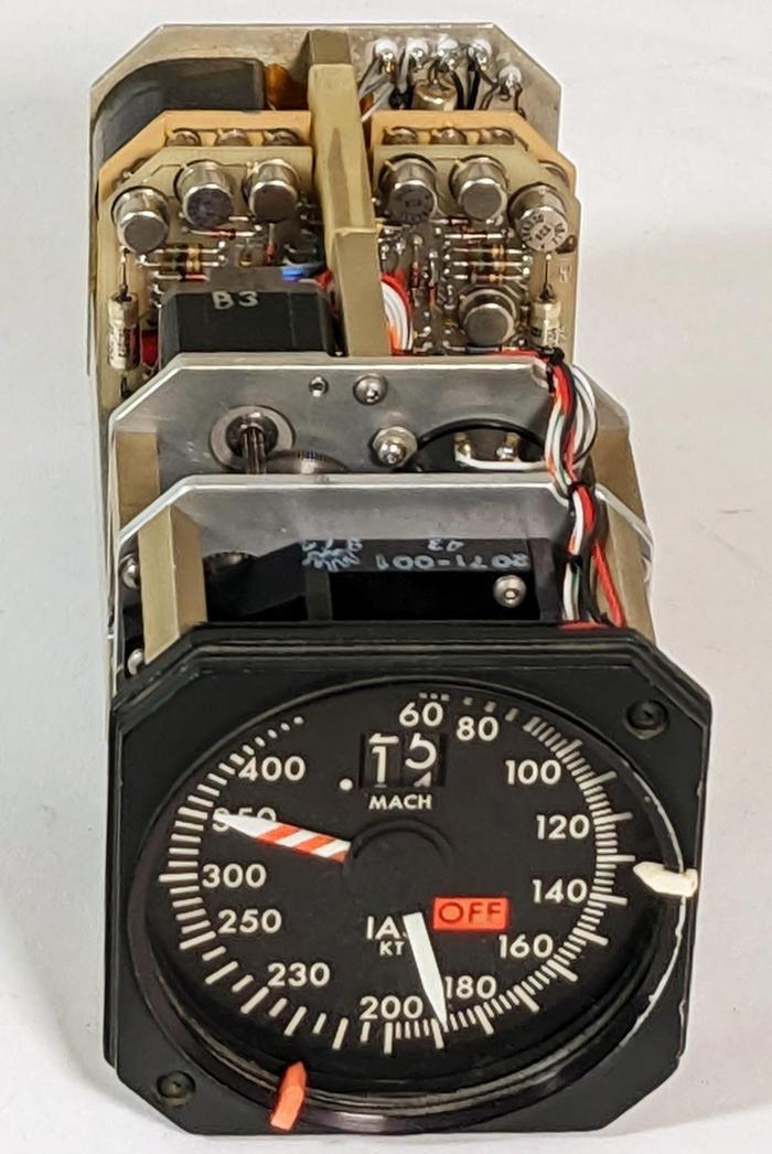
With the unit's cover removed, you can see the internal mechanisms and circuitry. Each of the three indicators is controlled by a small DC motor with a potentiometer providing feedback. To the right, two circuit boards provide the electronics to drive the indicators.4 At the upper right, the black blob is a 26-volt 400-Hertz transformer to power the unit. Some power supply components are in front of it. Below the transformer is an orangish flexible printed-circuit board, which seems advanced for the timeframe. This flexible ribbon connects the transformer, the external connector, and the printed-circuit board sockets, providing the backplane for the system.

A side view of the unit shows the gears to control the indicators.

A side view of the unit shows the gears to control the indicators.

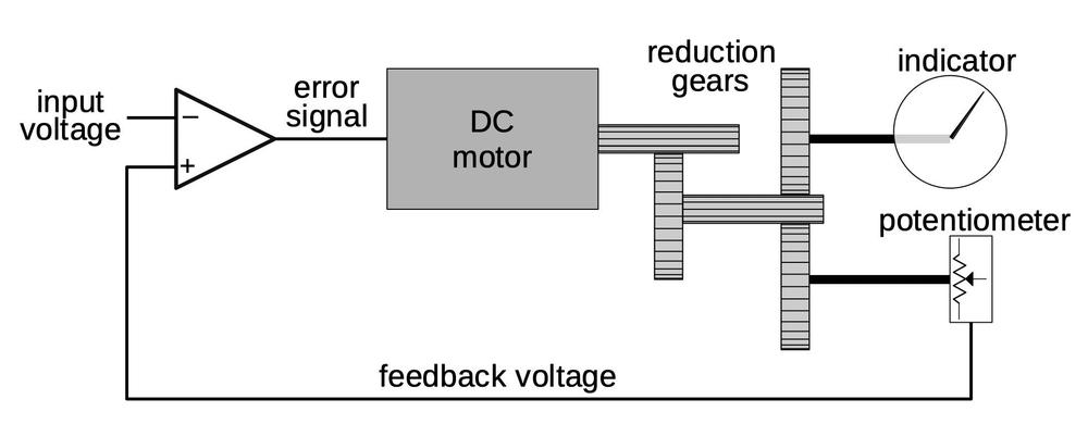
The diagram below shows the principle behind the servo mechanism that controls each indicator. The goal is to rotate the indicator to a position corresponding to the input voltage. A feedback loop is used to achieve this. The potentiometer provides a voltage proportional to its rotation. The input voltage and the feedback voltage are inputs to an op amp, which generates an error signal based on the difference between the inputs. The error signal rotates the DC motor in the appropriate direction until the potentiometer voltage matches the input voltage. Because the indicator and the potentiometer are geared together, the indicator will be in the correct position. As the input voltage changes, the system will continuously track the changes and keep the indicator updated.

A diagram illustrating the servo feedback loop.

A diagram illustrating the servo feedback loop.

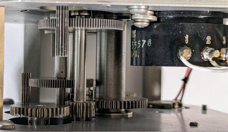
Because the DC motor spins much faster than the dial moves, reduction gears slow the rotation. The photo below shows the gear train in the unit. A potentiometer is at the upper-right with three wires attached.

A closeup of the gear train. A potentiometer is on the right.

A closeup of the gear train. A potentiometer is on the right.

The Mach number has additional gearing to rotate the numbered wheels. When the low-digit wheel cycles around, it advances the high-digit wheel, similar to an odometer.

The mechanism to rotate the digit wheels for the Mach number.

The mechanism to rotate the digit wheels for the Mach number.

Fault checking

One interesting feature of the indicator unit is that it implements fault checking to alert the pilot if something goes wrong. The front panel has a three-position flag. By default it's in the OFF position. Powering the coil in one direction rotates the flag to the blank side. Powering the coil in the other direction rotates the flag to the "VMO" position which indicates that the pilot has exceeded the maximum operating speed.

I figured that powering up the unit would move the flag out of the OFF position, but it's more complicated than that. First, the unit checks that the air data computer is providing a suitable reference voltage. Second, the unit verifies that the motor voltages for the two needles are within limits; this ensures that the servo loop is operating successfully. Third, the unit checks that signals are received on status pins K and L. The unit only moves out of the OFF state if all these conditions are satisfied.5 Thus, if the unit receives bad signals or is malfunctioning, the pilot will be alerted by the OFF indicator, rather than trusting the faulty display.

The circuitry

The unit is powered by 26 volts, 400 Hz, a standard voltage for aviation. A small transformer provides multiple outputs for the various internal voltages. The unit has four power supplies: three on the first board and one on the back wall of the unit. One power supply is for the status indicator, one is for the op amps, one powers the 41.7V motors, and the fourth provides other power.

One subtlety is how the feedback potentiometers are powered. The servo loop compares the potentiometer voltage with the input voltage. But this only works if the potentiometer and the input voltage are using the same reference. One solution would be for the indicator unit and the air data computer to contain matching precision voltage regulators. Instead, the system uses a simpler, more reliable approach: the air data computer provides a reference voltage that the indicator unit uses to power the potentiometers.6 With this approach, the air data computer's voltage reference can fluctuate and the indicator will still reach the right position. (In other words, a 5V input with a 10V reference and a 6V input with a 12V reference are both 50%.)

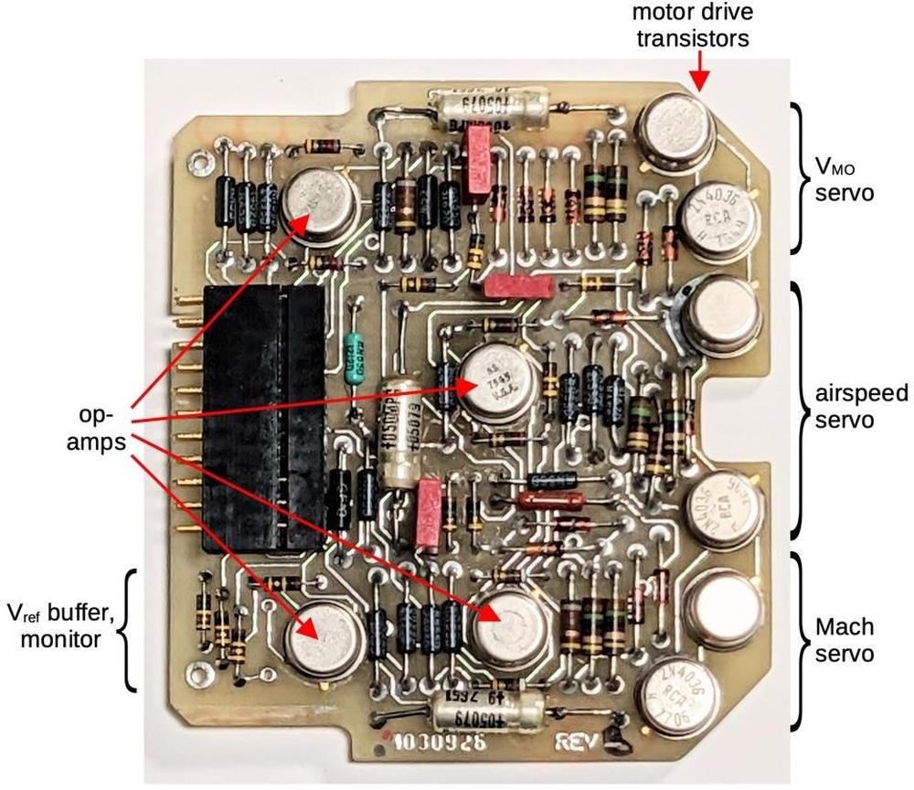
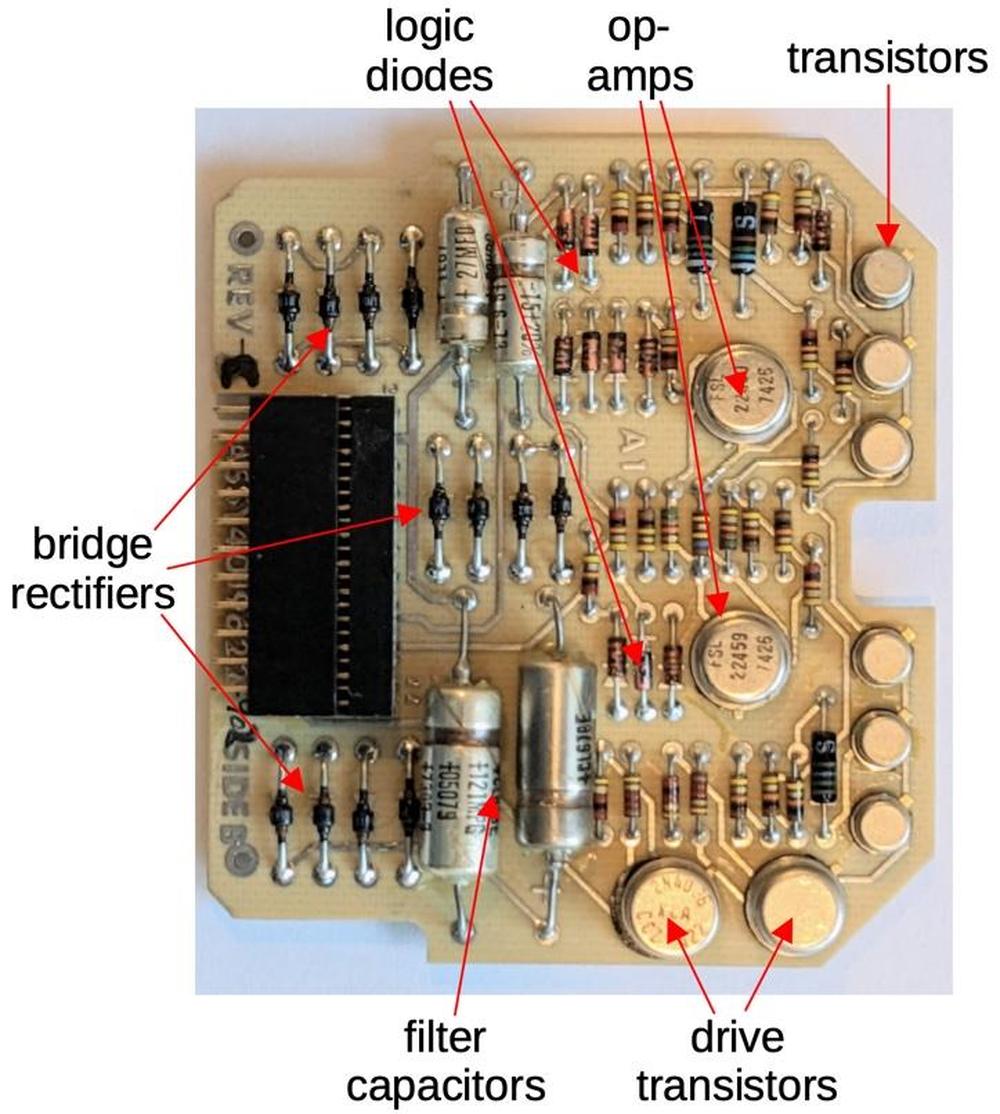
The diagram below shows the board with the servo circuitry. The board uses dual op-amp integrated circuits, packaged in 10-pin metal cans that protected against interference.7 The ICs and some of the other components have obscure military part numbers; I don't know if this unit was built for military use or if military-grade parts were used for reliability.

The servo board is full of transistors, resistors, capacitors, diodes, and op-amp integrated circuits.

The servo board is full of transistors, resistors, capacitors, diodes, and op-amp integrated circuits.

The circuitry in the lower-left corner handles the reference voltage from the air data computer. The board buffers this voltage with an op amp to power the three feedback potentiometers. The op amp also ensures that the reference voltage is at least 10 volts. If not, the indicator unit shows the "OFF" flag to alert the pilot.

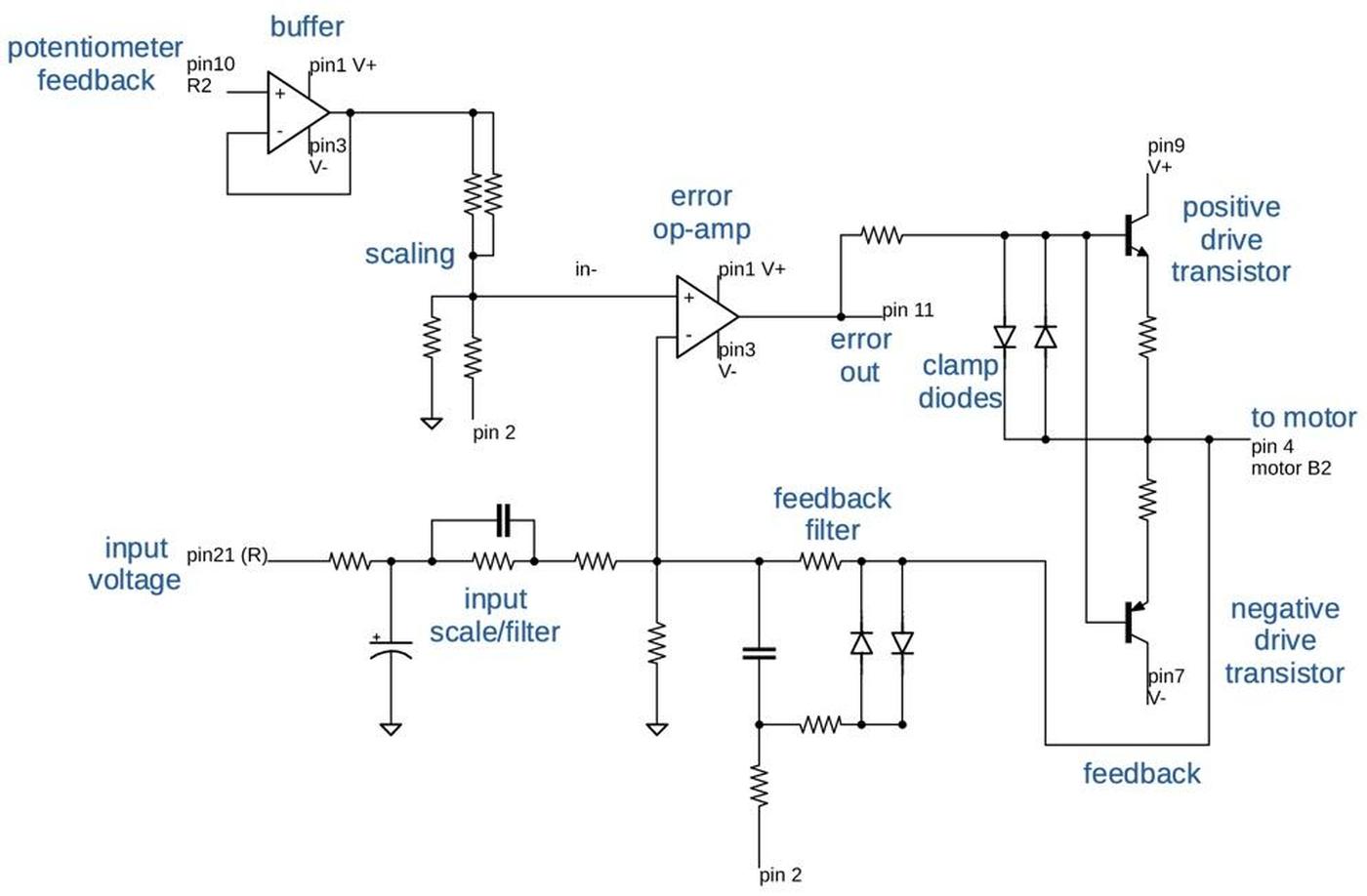
The schematic below shows one of the servo circuits; the three circuits are roughly the same. The heart of the circuit is the error op amp in the center. It compares the voltage from the potentiometer with the input voltage and generates an error output that moves the motor appropriately. A positive error output will turn on the upper transistor, driving the motor with a positive voltage. Conversely, a negative error output will turn on the lower transistor, driving the motor with a negative voltage. The motor drive circuit has clamp diodes to limit the transistor base voltages.

Schematic of one of the servo circuits.

Schematic of one of the servo circuits.

The op amp also receives a feedback signal from the motor output. I don't entirely understand this signal, which goes through a filter circuit with resistors, diodes, and a capacitor. I think it dampens the motor signal so the motor doesn't overshoot the desired position. I think it also keeps the transistor drive signal biased relative to the emitter voltage (i.e. the motor output).

On the input side, the potentiometer voltage goes through an op amp follower buffer, which simply outputs its input voltage. This may seem pointless, but the op amp provides a high-impedance input so the potentiometer's voltage doesn't get distorted.

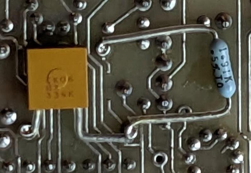
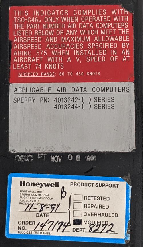
The external input voltage goes through a resistor/capacitor circuit to scale it and filter out noise. Curiously, the circuit board was modified by cutting a trace and adding a resistor and capacitor to change the input circuit for one of the inputs. In the photo below, you can see the added resistor and capacitor; the cut trace is just to the right of the capacitor. I don't know if this modification changed the scale factor or if it filtered out noise. A label on the box says that Honeywell performed a modification on November 8, 1991, which presumably was this circuit.

A closeup of the circuit board showing the modification.

A closeup of the circuit board showing the modification.

The second board implements three power supplies as well as the circuitry for the OFF/VMO flag. The power supplies are simple and unregulated, just diode bridges to convert AC to DC, along with filter capacitors. Most of the circuitry on the board controls the status flag. Two dual op amps check the motor voltages against upper and lower limits to ensure that the motors are tracking the inputs. These outputs, along with other logic status signals, are combined with diode-transistor logic to determine the flag status. Driver transistors provide +18 or -18 volts to the flag's coil to drive it to the desired position.

This board has power supply circuitry and the control circuitry for the indicator flag.

This board has power supply circuitry and the control circuitry for the indicator flag.

Conclusions

After reverse-engineering the pinout, I connected the airspeed indicator to a stack of power supplies and succeeded in getting the indicators to operate (video). This unit is much more complex than I expected for a simple display, with servoed motors controlled by two boards of electronics. Air safety regulations probably account for much of the complexity, ensuring that the display provides the pilot with accurate information. For all that complexity, the unit is essentially a voltmeter, indicating three voltages on its display. This airspeed indicator is a bit different from most of the hardware I examine, but hopefully you found this look at its internal circuitry interesting.

With the case removed, the internal circuitry is visible.

With the case removed, the internal circuitry is visible.

You can follow me on Twitter @kenshirriff or rss. I've also started experimenting with mastodon recently as @oldbytes.space@kenshirriff.

Notes and references

  1. Since the unit has airspeed and maximum airspeed indicators, you might expect it to display the maximum airspeed warning flag based on the two speed inputs. Instead, the flag is controlled by input pin "L". In other words, the air data computer, not the indicator unit, determines when the maximum airspeed is exceeded. 

  2. This unit is a "Mach Airspeed Indicator", 4018366, apparently also called the SI-225,2

    Product label with part number 4018366-901.

    Product label with part number 4018366-901.

    Note that the label says Sperry. In 1986, Sperry attempted to buy Honeywell but instead Burroughs made a hostile takeover bid. The merger of Sperry and Burroughs formed Unisys. A couple of months after the merger, the Sperry Aerospace Group was sold to Honeywell for $1.025 billion. Thus, the indicator became a Honeywell product. This corporate history explains why the unit has a Honeywell product support sticker.

    Labels on top of the unit indicate that it worked with the Sperry 4013242 and 4013244 air data computers. These became the Honeywell AZ-242 and AZ-244.

    Labels on top of the unit indicate that it worked with the Sperry 4013242 and 4013244 air data computers. These became the Honeywell AZ-242 and AZ-244.


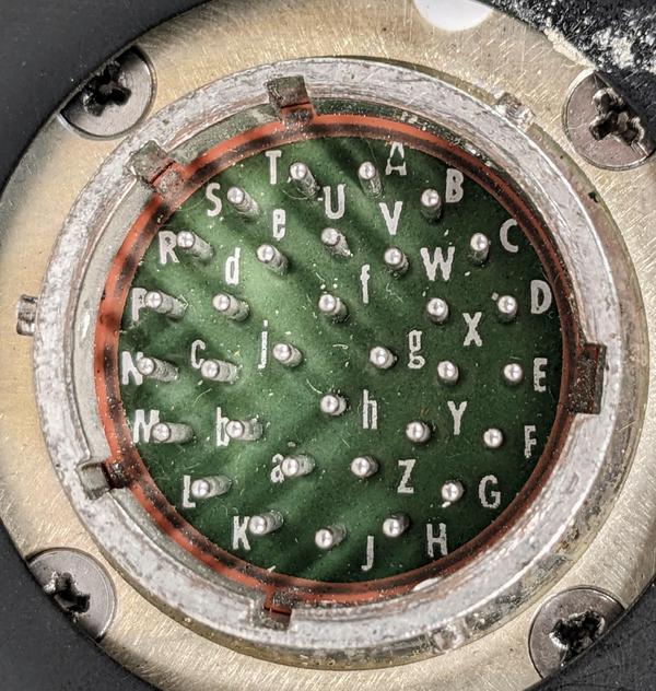
  3. The connector is a 32-pin MIL Spec round connector. Most of the 32 pins are unused. The connector has complex keying with 5 slots. I assume the keying is specific to this indicator, so the wrong indicator doesn't get connected.

    A closeup of the 32-pin connector, probably a MIL Spec 18-32.

    A closeup of the 32-pin connector, probably a MIL Spec 18-32.

    For reference, here is the pinout of the unit. Since this is based on reverse engineering, I don't guarantee it 100%. Don't use this for flight!

    PinUse
    A5V illumination
    BChassis ground
    CAC ground
    E26V 400 Hz
    F26V 400 Hz
    KEnable
    LSpeed ok
    MSignal ground
    NRef. voltage
    PVmax control voltage
    RAirspeed control voltage
    SMach control voltage
    VChassis ground

    Pins D, G, H, J, T, U, W, X, Y, Z, a, b, c, d, e, f, g, h, and j are unused. 

  4. The chassis has an empty slot for a third circuit board. My guess is that this chassis was used for multiple types of indicators and others required a third board. 

  5. If the L pin goes low, the indicator will move to the VMO position. 

  6. My hypothesis is that the correct reference voltage is 11.7 volts. This yields a scale factor of 1 volt equals 50 knots. It also matches up the display's change in scale at 250 knots with the measured scale change. 

  7. The meter uses three different integrated circuits in 10-pin metal cans with mysterious military markings: "FHL 24988", "JM38510/10102BIC 27014", and "SL14040". These appear to all be equivalent to uA747 dual op amps. (Note that JM38510 is not a part number; it is a general military specification for integrated circuits. The number after it is the relevant part number.) 

The 8086 processor's microcode pipeline from die analysis

Intel introduced the 8086 microprocessor in 1978, and its influence still remains through the popular x86 architecture. The 8086 was a fairly complex microprocessor for its time, implementing instructions in microcode with pipelining to improve performance. This blog post explains the microcode operations for a particular instruction, "ADD immediate". As the 8086 documentation will tell you, this instruction takes four clock cycles to execute. But looking internally shows seven clock cycles of activity. How does the 8086 fit seven cycles of computation into four cycles? As I will show, the trick is pipelining.

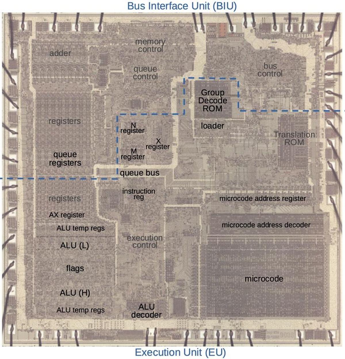
The die photo below shows the 8086 microprocessor under a microscope. The metal layer on top of the chip is visible, with the silicon and polysilicon mostly hidden underneath. Around the edges of the die, bond wires connect pads to the chip's 40 external pins. Architecturally, the chip is partitioned into a Bus Interface Unit (BIU) at the top and an Execution Unit (EU) below, which will be important in the discussion. The Bus Interface Unit handles memory accesses (including instruction prefetching), while the Execution Unit executes instructions. The functional blocks labeled in black are the ones that are part of the discussion below. In particular, the registers and ALU (Arithmetic/Logic Unit) are at the left and the large microcode ROM is in the lower-right.

The 8086 die under a microscope, with main functional blocks labeled. This photo shows the chip's single metal layer; the polysilicon and silicon are underneath. Click on this image (or any other) for a larger version.

The 8086 die under a microscope, with main functional blocks labeled. This photo shows the chip's single metal layer; the polysilicon and silicon are underneath. Click on this image (or any other) for a larger version.

Microcode for "ADD"

Most people think of machine instructions as the basic steps that a computer performs. However, many processors (including the 8086) have another layer of software underneath: microcode. The motivation is that instructions usually require multiple steps inside the processor. One of the hardest parts of computer design is creating the control logic that directs the processor for each step of an instruction. The straightforward approach is to build a circuit from flip-flops and gates that moves through the various steps and generates the control signals. However, this circuitry is complicated, error-prone, and hard to design.

The alternative is microcode: instead of building the control circuitry from complex logic gates, the control logic is largely replaced with code. To execute a machine instruction, the computer internally executes several simpler micro-instructions, specified by the microcode. In other words, microcode forms another layer between the machine instructions and the hardware. The main advantage of microcode is that it turns the processor's control logic into a programming task instead of a difficult logic design task.

The 8086 uses a hybrid approach: although the 8086 uses microcode, much of the instruction functionality is implemented with gate logic. This approach removed duplication from the microcode and kept the microcode small enough for 1978 technology. In a sense the microcode is parameterized. For instance, the microcode can specify a generic ALU operation, and the gate logic determines from the instruction which ALU operation to perform. Likewise, the microcode can specify a generic register and the gate logic determines which register to use. The simplest instructions (such as prefixes or condition-code operations) don't use microcode at all. Although this made the 8086's gate logic more complicated, the tradeoff was worthwhile.

The 8086's microcode was disassembled by Andrew Jenner (link) from my die photos, so we can see exactly what micro-instructions the 8086 is running for each machine instruction. In this post, I will focus on the ADD instruction, since it is fairly straightforward. In particular, the "ADD AX, immediate" instruction contains a 16-bit value that is added to the value in the 16-bit AX register. This instruction consists of three bytes: the opcode 05, followed by the two-byte immediate value. (An "immediate" value is included in the instruction, rather than coming from a register or memory location.)

This ADD instruction is implemented in the 8086's microcode as four micro-instructions, shown below. Each micro-instruction specifies a move operation across the internal ALU bus. It also specifies an action. In brief, the first two instructions get the immediate argument from the prefetch queue. The third instruction gets the argument from the AX register and starts the ALU (Arithmetic/Logic Unit) operation. The final instruction stores the result into the AX register and updates the condition flags.

µ-address    move        action
   018    Q → tmpBL     L8    2
   019    Q → tmpBH
   01a    M → tmpA      XI    tmpA, NXT
   01b    Σ → M         RNI   FLAGS

In detail, the first instruction moves a byte from the prefetch queue (Q) to one of the ALU's temporary registers, specifically the low byte of the tmpB register. (The ALU has three temporary registers to hold arguments: tmpA, tmpB, and tmpC. These temporary registers are invisible to the programmer and are unrelated to the AX, BX, CX registers.) Likewise, the second instruction fetches the high byte of the immediate value from the queue and stores it in the high byte of the ALU's tmpB register. The action in the first micro-instruction, L8, will branch to step 2 (01a) if the instruction specifies an 8-bit operation, skipping the load of the high byte. Thus, the same microcode supports the 8-bit and 16-bit ADD instructions.1

The third micro-instruction is more complicated. The move section moves the AX register's contents (indicated by M) to the accumulator's tmpA register, getting both arguments ready for the operation. XI tmpA starts an ALU operation, in this case adding tmpA to tmpB.2 Finally, NXT indicates that this is the next-to-last micro-instruction, as will be discussed below.

The last micro-instruction stores the ALU's result (Σ) into the AX register. The end of the microcode for this machine instruction is indicated by RNI (Run Next Instruction). Finally, FLAGS causes the 8086's condition flags register to be updated, indicating if the result is zero, negative, and so forth.

You may have noticed that the microcode doesn't explicitly specify the ADD operation or the AX register, using XI and M instead. This illustrates the "parameterized" microcode mentioned earlier. The microcode specifies a generic ALU operation with XI,3 and the hardware fills in the particular ALU operation from bits 5-3 of the machine instruction. Thus, the microcode above can be used for addition, subtraction, exclusive-or, comparisons, and four other arithmetic/logic operations.

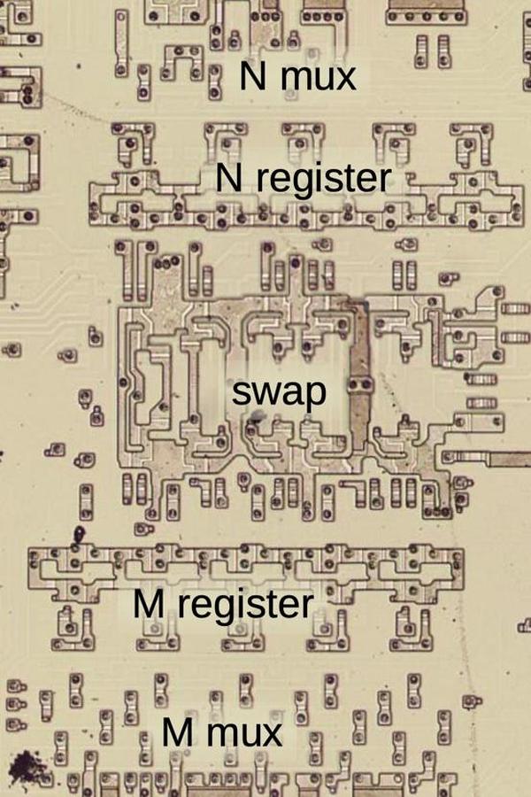
The other parameterized aspect is the generic M register specification. The 8086's instruction set has a flexible way of specifying registers for the source and destination of an operation: registers are often specified by a "Mod R/M" byte, but can also be specified by bits in the first opcode. Moreover, many instructions have a bit to switch the source and destination, and another bit to specify an 8-bit or 16-bit register. The microcode can ignore all this; a micro-instruction uses M and N for the source and destination registers, and the hardware handles the details.4 The M and N values are implemented by 5-bit registers that are invisible to the programmer and specify the "real" register to use. The diagram below shows how they appear on the die.

Die photo of the circuitry that implements the M and N registers. A multiplexer selects a source for the N register value and feeds it into the 5-bit N register. The M register is similar. Between the two registers is a "swap" circuit to swap the outputs of the two registers based on the instruction's "direction" bit. In this image, the metal layer has been dissolved with acid to show the transistors in the silicon layer underneath.

Die photo of the circuitry that implements the M and N registers. A multiplexer selects a source for the N register value and feeds it into the 5-bit N register. The M register is similar. Between the two registers is a "swap" circuit to swap the outputs of the two registers based on the instruction's "direction" bit. In this image, the metal layer has been dissolved with acid to show the transistors in the silicon layer underneath.

Pipelining

The 8086 documentation says this ADD instruction takes four clock cycles, and as we have seen, it is implemented with four micro-instructions. One micro-instruction is executed per clock cycle, so the timing seems straightforward. The problem, however, is that a micro-instruction can't be completed in one clock cycle. It takes a clock cycle to read a micro-instruction from the microcode ROM. Sending signals across an internal bus typically takes a clock cycle and other actions take more time. So a typical micro-instruction ends up taking 2½ clock cycles from start to end. One solution would be to slow down the clock, so the micro-instruction can complete in one cycle, but that would drastically reduce performance. A better solution is pipelining the execution so a micro-instruction can complete every cycle.5

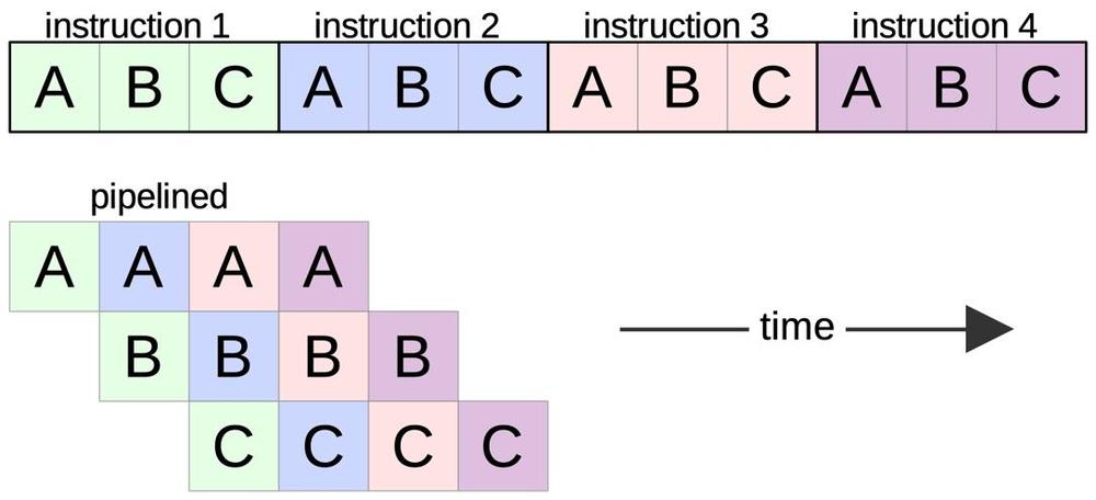
The idea of pipelining is to break instruction processing into "stages", so different stages can work on different instructions at the same time. It's sort of like an assembly line, where a particular car might take an hour to manufacture, but a new car comes off the assembly line every minute. The diagram below shows a simple example. Suppose executing an instruction requires three steps: A, B, and C. Executing four instructions, as shown at the top would take 12 steps in total.

Diagram of a simple pipeline showing four instructions executing through three stages.

Diagram of a simple pipeline showing four instructions executing through three stages.

However, suppose the steps can execute independently, so step B for one instruction can execute at the same time as step A for another instruction. Now, as soon as instruction 1 finishes step A and moves on to step B, instruction 2 can start step A. Next, instruction 3 starts step A as instructions 2 and 1 move to steps B and C respectively. The first instruction still takes 3 time units to complete, but after that, an instruction completes every time unit, providing a theoretical 3× speedup.6 In a bit, I will show how the 8086 uses the idea of pipelining.

The prefetch queue

The 8086 uses instruction prefetching to improve performance. Prefetching is not the focus of this article, but a brief explanation is necessary. (I wrote about the prefetch circuitry in detail earlier.) Memory accesses on the 8086 are relatively slow (at least four clock cycles), so we don't want to wait every time the processor needs a new instruction. The idea behind prefetching is that the processor fetches future instructions from memory while the CPU is busy with the current instruction. When the CPU is ready to execute the next instruction, hopefully the instruction is already in the prefetch queue and the CPU doesn't need to wait for memory. The 8086 appears to be the first microprocessor to implement prefetching.

In more detail, the 8086 fetches instructions into its prefetch queue asynchronously from instruction execution: The "Bus Interface Unit" performs prefetches, while the "Execution Unit" executes instructions. Prefetched instructions are stored in the 6-byte prefetch queue. The Q bus (short for "Queue bus") provides bytes, one at a time, from the prefetch queue to the Execution Unit.7 If the prefetch queue doesn't have a byte available when the Execution Unit needs one, the Execution Unit waits until the prefetch circuitry can complete a memory access.

The loader

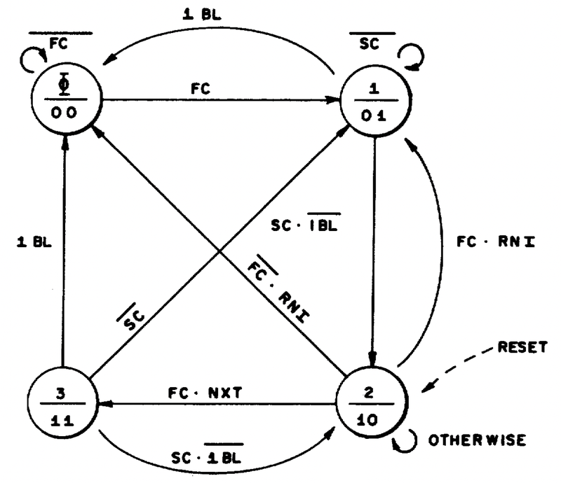
To decode and execute an instruction, the Execution Unit must get instruction bytes from the prefetch queue, but this is not entirely straightforward. The main problem is that the prefetch queue can be empty, blocking execution. Second, instruction decoding is relatively slow, so for maximum performance, the decoder needs a new byte before the current instruction is finished. A circuit called the "loader" solves these problems by using a small state machine (below) to efficiently fetch bytes from the queue at the right time.

The state machine for the 8086 "loader" circuit. I'm not going to explain how it works in this post, but the diagram looks pretty cool.
From patent US4449184.

The state machine for the 8086 "loader" circuit. I'm not going to explain how it works in this post, but the diagram looks pretty cool. From patent US4449184.

The loader generates two timing signals that synchronize instruction decoding and microcode execution with the prefetch queue. The FC (First Clock) indicates that the first instruction byte is available, while the SC (Second Clock) indicates the second instruction byte. Note that the First Clock and Second Clock are not necessarily consecutive clock cycles because the first byte could be the last one in the queue, delaying the Second Clock.

At the end of a microcode sequence, the Run Next Instruction (RNI) micro-operation causes the loader to fetch the next machine instruction. However, microcode execution would be blocked for a cycle due to the delay of fetching and decoding the next instruction. In many cases, this can be avoided: if the microcode knows that it is one micro-instruction away from finishing, it issues a Next-to-last (NXT) micro-operation so the loader can start loading the next instruction before the previous instruction finishes. As will be shown in the next section, this usually allows micro-instructions to run without interruption.

Instruction execution

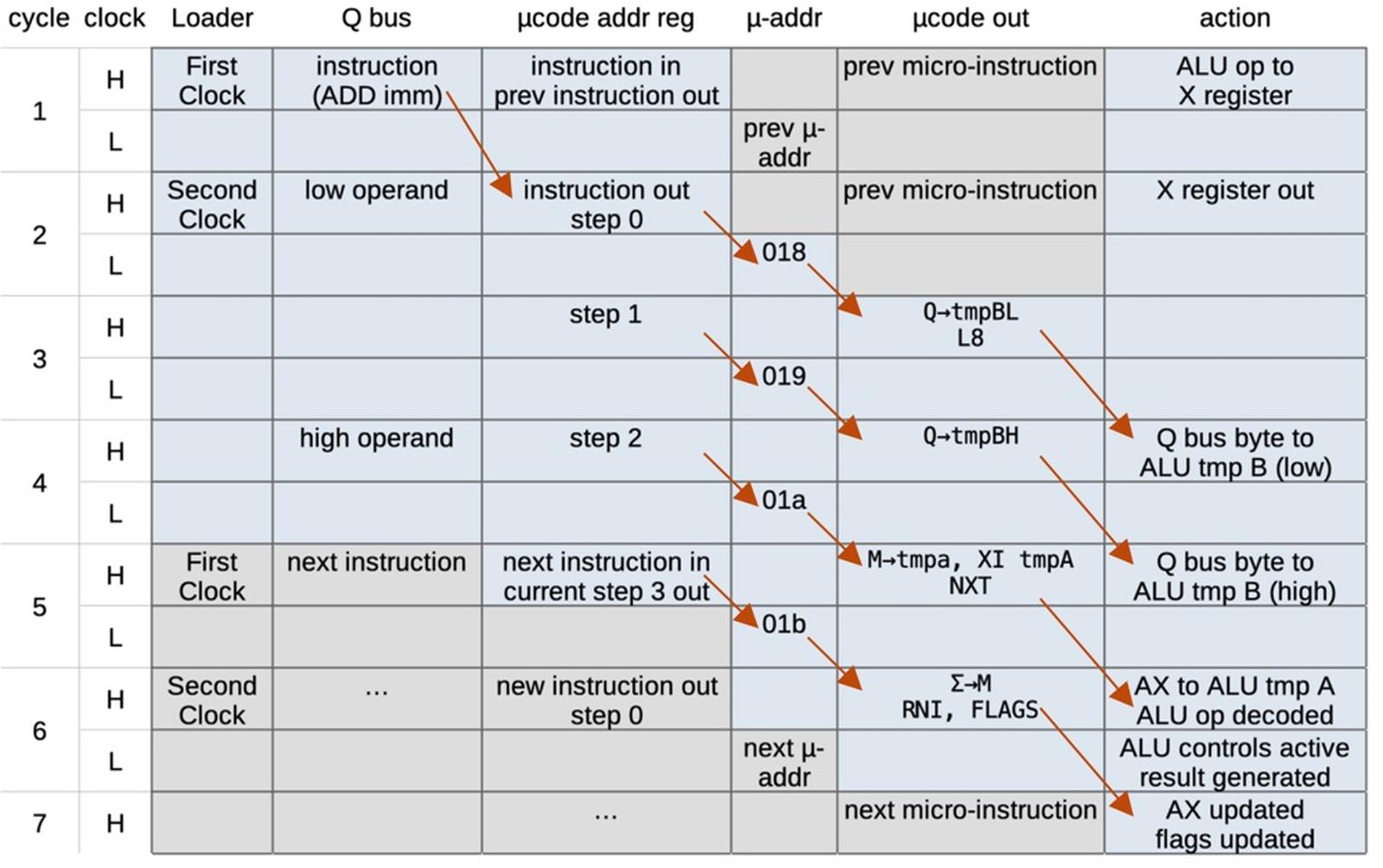
Putting this all together, we can see how the ADD instruction is executed, cycle by cycle. Each clock cycle starts with the clock high (H) and ends with the clock low (L).8 The sequence starts with the prefetch queue supplying the ADD instruction across the Q bus in cycle 1. The loader indicates that this is First Clock and the instruction is loaded into the microcode address register. It takes a clock cycle for the address to exit the address register (as indicated by an arrow) along with the microcode counter value indicating step 0. To remember the ALU operation, bits 5-3 of the instruction are saved in the internal X register (unrelated to the AX register).

In cycle 2, the prefetch queue has supplied the second byte of the instruction so the loader indicates Second Clock. In the second half of cycle 2, the microcode address decoder has converted the instruction-based address to the micro-address 018 and supplies it to the microcode ROM.

In cycle 3, the microcode ROM outputs the micro-instruction at micro-address 018: Q→tmpBL, which will move a byte from the prefetch queue bus (Q bus) to the low byte of the ALU temporary B register, as described earlier. It takes a full clock cycle for this action to take place, as the byte traverses buses to reach the register. This micro-instruction also generates the L8 micro-op, which will branch if an 8-bit operation is taking place. As this is a 16-bit operation, no branch takes place.9 Meanwhile, the microcode address register moves to step 1, causing the decoder to produce the micro-address 019.

This diagram shows the execution of an ADD instruction and what is happening in various parts of the 8086. The arrows show the flow from step to step. The character µ is short for "micro".

This diagram shows the execution of an ADD instruction and what is happening in various parts of the 8086. The arrows show the flow from step to step. The character µ is short for "micro".

In cycle 4, the prefetch queue provides a new byte, the high byte of the immediate value. The microcode ROM outputs the micro-instruction at micro-address 019: Q→tmpBH, which will move this byte from the prefetch queue bus to the high byte of the ALU temporary B register. As before, it takes a full cycle for this move to complete. Meanwhile, the microcode address register moves to step 2, causing the decoder to produce the micro-address 01a.

In cycle 5, the microcode ROM outputs the micro-instruction at micro-address 01a: M→tmpA,XI tmpA,NXT. Since the M (source) register specifies AX, the contents of the AX register will be moved into the ALU tmpA register, but this will take a cycle to complete. The XI tmpA part starts decoding the ALU operation saved in the X register, in this case ADD. Finally, NXT indicates that the next micro-instruction is the last one in this instruction. In combination with the next instruction on the Q bus, this causes the loader to issue First Clock. This starts execution of the next machine instruction, even though the current instruction is still executing.

In cycle 6, the microcode ROM outputs the micro-instruction at micro-address 01b: Σ→M,RNI. This will store the ALU output into the register indicated by M (i.e. AX), but not yet. In the first half of cycle 6, the ALU decoder determines the ALU control signals that will cause an ADD to take place. In the second half of cycle 6, the ALU receives these control signals and computes the sum. The RNI (Run Next Instruction) and the second instruction byte from the prefetch queue cause the loader to issue Second Clock, and the micro-address for the next machine instruction is sent to the microcode ROM.

Finally, in cycle 7, the sum is written to the AX register and the flags are updated, completing the ADD instruction. Meanwhile, the next instruction is well underway with its first micro-instruction being executed.

As you can see, execution of a micro-instruction is pipelined, with three full clock cycles from the arrival of an instruction until the first micro-instruction completes in cycle 4. Although this system is complex, in the best case it achieves the goal of running a micro-instruction each cycle, without gaps. (There are gaps in some cases, most commonly when the prefetch queue is empty. A gap will also occur if the microcode control flow doesn't allow a NXT micro-instruction to be issued. In that case, the loader can't issue First Clock until the RNI micro-instruction is issued, resulting in a delay.)

Conclusions

The 8086 uses multiple types of pipelining to increase performance. I've focused on the pipelining at the microcode level, but the 8086 uses at least four interlocking types of pipelining. First, microcode pipelining allows micro-instructions to complete at the rate of one per clock cycle, even though it takes multiple cycles for a micro-instruction to complete. Admittedly, this pipeline is not very deep compared to the pipelines in RISC processors; the 8086 designers called the overlap in the microcode ROM a "sort of mini-pipeline."10

The second type of pipelining overlaps instruction decoding and execution. Instruction decoding is fairly complicated on the 8086 since there are many different formats of instructions, usually depending on the second byte (Mod R/M). The loader coordinates this pipelining, issuing the First Clock and Second Clock signals so decoding on the next instruction can start before the previous instruction has completed. Third is the prefetch queue, which overlaps fetching instructions from memory with execution. This is accomplished by partitioning the processor into the Bus Interface Unit and the Execution Unit, with the prefetch queue in between. (I recently wrote about instruction prefetching in detail.)

There's a final type of pipelining that I haven't discussed. Inside the memory access sequence, computing the memory address from a segment register and offset is overlapped with the previous memory access. The result is that memory accesses appear to take four cycles, even though they really take six cycles. I plan to write more about memory access in a later post.

The 8086 was a large advance in size, performance, and architecture compared to earlier microprocessors such as the Z80 (1976), 8085 (1977), and 6809 (1978). As well as moving to 16 bits, the 8086 had a considerably more complex architecture with instruction prefetching and microcode, among other features. At the same time, the 8086 avoided the architectural overreach of Intel's ill-fated iAPX 432, a complex processor that supported garbage collection and objects in hardware. Although the 8086's architecture had flaws, it was a success and led to the x86 architecture, still dominant today.

I plan to continue reverse-engineering the 8086 die so follow me on Twitter @kenshirriff or RSS for updates. I've also started experimenting with Mastodon recently as @oldbytes.space@kenshirriff. If you're interested in the 8086, I wrote about the 8086 die, its die shrink process and the 8086 registers earlier.

Notes and references

  1. The lowest bit of many 8086 instructions selects if the instruction operates on a byte or a word. Thus, many instructions in the instruction set appear in pairs. The support for byte operations gave the 16-bit 8086 processor compatibility with the older 8-bit 8080, if assembly code was suitably translated. 

  2. The microcode for an ALU operation can select the first operand from tmpA, tmpB, or tmpC. The second operand is always tmpB. 

  3. I don't know why Intel used XI to indicate the ALU opcode. I don't think it's the Greek letter Ξ, although they did use Σ (sigma) for the ALU output. The opcode is stored in the X register, so maybe XI is X Instruction? (It's also unclear why the register is called X.) 

  4. Normally, the internal M register specifies the source register and the N register specifies the destination register, and these two registers are loaded from the instruction. However, some instructions only use the A or AX register, depending on whether the instruction acts on bytes or words. These instructions are the ALU immediate instructions, accumulator move instructions, string instructions, and the TEST, IN, and OUT instructions. For these instructions, the Group Decode ROM activates a signal that forces the M register to specify the AX register for a 16-bit operation, or the A register for an 8-bit operation. Thus, by specifying the M register in the microcode above, the same microcode is used for instructions with an 8-bit immediate argument or a 16-bit immediate argument. This also illustrates how the designers of the 8086 kept the microcode small by moving a lot of logic into hardware. 

  5. I should mention that the pipelining in the 8086 is completely different from the parallelism in modern superscalar CPUs. The 8086 is executing instructions linearly, step-by-step, even though instructions overlap. There is only one execution path and no speculative execution, for instance. 

  6. I showed a theoretical speedup from pipelining. Several issues make the real speedup smaller. First, the steps of an instruction typically don't take the same amount of time, so you're limited by the slowest step. Second, the overhead to handle the steps adds some delay. Finally, conflicts between instructions and other "hazards" may prevent overlap in various cases. 

  7. The interaction between the prefetch queue and the Execution Unit is a "push" model rather than a "pull" model. If the prefetch queue contains a byte, the prefetch circuitry puts the byte on the Q bus and lets the Execution Unit know that a byte is available. The Execution Unit signals the prefetch circuitry when it uses a byte, and the prefetch queue moves to the next byte in the queue. If the Execution Unit needs a byte and it isn't ready, it blocks until a byte is available. The prefetch queue loads new words as it empties, when the memory bus isn't in use for other purposes. 

  8. The 8086 is active during both phases (low and high) of the clock, with things happening both while the clock is high and while it is low. One unusual feature of the 8086 is that the clock signal is asymmetrical with a 33% duty cycle, so the clock is low for twice as long as the clock is high. In other words, the 8086 does twice as much (by time) during the low part of the clock cycle as during the high part of the clock cycle. There are multiple reasons why actions take a full clock cycle to complete. Much of the circuitry uses edge-triggered flip-flops to hold state. These latch data on one clock edge and move data internally during the other part of the clock. (The 8086 uses both positive-edge and negative-edge triggered flip flops; some latch when the clock goes high and others latch when the clock goes low.) Many control signals have their voltage level boosted by a bootstrap driver circuit, driven by the clock.

    Many buses are precharged during one clock phase and then transmit a signal during the other phase. The motivation behind precharging the bus is that NMOS transistors are much better at pulling a line low than pulling it high (i.e. they can provide more current). This especially affects buses because they have relatively high capacitance due to their length, so pulling the bus high is slow. Thus, the bus is "leisurely" precharged to a high state during one clock phase, and then it can be rapidly pulled low (if the bit is a 0) and transmit the data during the other clock phase. 

  9. You might expect that the 8-bit ADD would be faster than the 16-bit ADD since it is a 2-byte instruction instead of a 3-byte instruction and one micro-instruction is skipped. However, both the 8-bit and the 16-bit ADD instructions take 4 cycles. The reason is that branching to a new micro-instruction requires updating the microcode address register, which takes a clock cycle, resulting in a wasted clock cycle where no micro-instruction is executed. (Specifically, the next micro-instruction is on the way, so it is blocked by the ROM Enable (ROME) signal going low.) The result of this is that the branch for an 8-bit ADD costs an extra cycle, which cancels out the saved cycle. (In practice, the 16-bit instruction might be slower because it needs one more byte from the prefetch queue, which could cause a delay.) Just as a branch in the machine instructions can cause a delay (a "bubble") in the instruction pipeline, a branch in the microcode causes a delay in the micro-instruction pipeline. 

  10. The design decisions for the 8086 are described in: J. McKevitt and J. Bayliss, "New options from big chips," in IEEE Spectrum, vol. 16, no. 3, pp. 28-34, March 1979, doi: 10.1109/MSPEC.1979.6367944.