X-ray reverse-engineering a hybrid module from 1960s Apollo test equipment

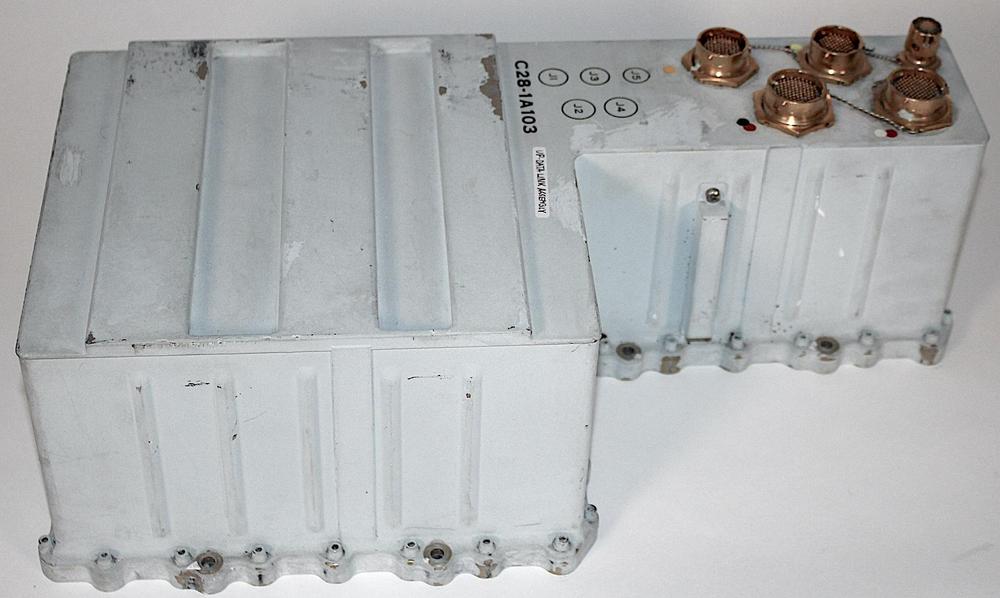
In this blog post, I reverse-engineer a hybrid module that was used for ground-testing of equipment from the Apollo space program. But first, some background. During the Apollo missions to the Moon, NASA could send digital messages to the spacecraft from the ground. These data messages could perform specific tasks: control spacecraft equipment by activating relays, send commands directly to the Apollo Guidance Computer, or even set the spacecraft's clock. Onboard the Command Module, these messages were decoded by the Up-Data Link, a drab bluish box (below) mounted in the equipment bay.

The Up-Data Link (UDL) was installed on the Apollo Command Module.

The Up-Data Link (UDL) was installed on the Apollo Command Module.

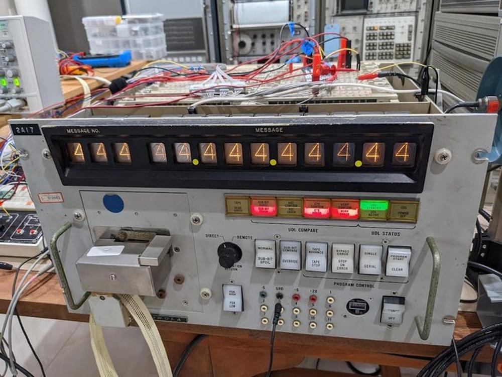
To ensure a successful mission, all the systems of Apollo were thoroughly tested on the ground before flight. The Up-Data Link was tested with the box below, labeled "Up-Data Link Confidence Test Set". Our friend Marcel obtained this box at a scrapyard, so we set out to make it work, but unfortunately it had no documentation and a few missing components. After reverse-engineering its complex circuitry and performing some repairs, we figured out how it works: The test box read a command from paper tape, encoded it for radio transmission using phase-shift keying, fed the signal into the up-data link box, and then verified that the up-data link box took the proper action. The transmitted message was shown on the display, while the red and green status lights indicated if the operation was decoded successfully. Thus, the test box provided an automated system for exercising the functions of the up-data link.

The up-data test box is a heavy rack-mounted box full of circuitry. The wiring on top is for our reverse-engineering, plugged into the box's numerous test points.

The up-data test box is a heavy rack-mounted box full of circuitry. The wiring on top is for our reverse-engineering, plugged into the box's numerous test points.

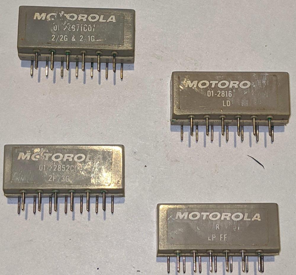
The construction of the test box was very unusual from a modern perspective. The box was constructed from 25 printed-circuit boards, with the boards connected by a tangled backplane of point-to-point wiring. Each board held up to 18 gray rectangular modules, blocks that look a bit like relays but contain electronic circuitry. These modules were built by Motorola and had labels that indicated the type of module; the photo below shows some of these compact modules, each 1.5" long. On the underside of the module, 13 pins in two unequal rows were plugged into a socket on the circuit board.

Some of the Motorola modules: 2/2G&2/1G, LD, 2P/3G, and LP FF. The printing for the part numbers smudges very easily.

Some of the Motorola modules: 2/2G&2/1G, LD, 2P/3G, and LP FF. The printing for the part numbers smudges very easily.

Why would a complex electronic box be built from modules instead of integrated circuits? The invention of the integrated circuit in 1958 led to an electronic revolution, but in the mid-1960s integrated circuits were still expensive and rare. An alternative was small hybrid modules that functioned as building blocks: logic gates, flip flops, op-amps, and other circuits. Instead of a silicon chip, these hybrid modules contained discrete transistors, resistors, capacitors, and other components.

I could find no documentation on these Motorola modules, or even a mention of them, despite my best efforts with Google and Bitsavers. However, the modules could be easily removed from the sockets for experimentation, with the unexpected convenience that the 0.200" pin spacing is compatible with modern solderless breadboards. For most of the modules, I could determine their function by probing them with test signals, in combination with examining their surrounding circuitry, which showed standardized +6 and -6 volt power supply connections. The modules had simple logic functions hinted at by the labels: for instance, the "LP FF" was a (low-power? low-performance?) flip flop while "2/2G & 2/1G" indicated a module with two 2-input NAND gates and two 1-input gates (i.e. inverters).

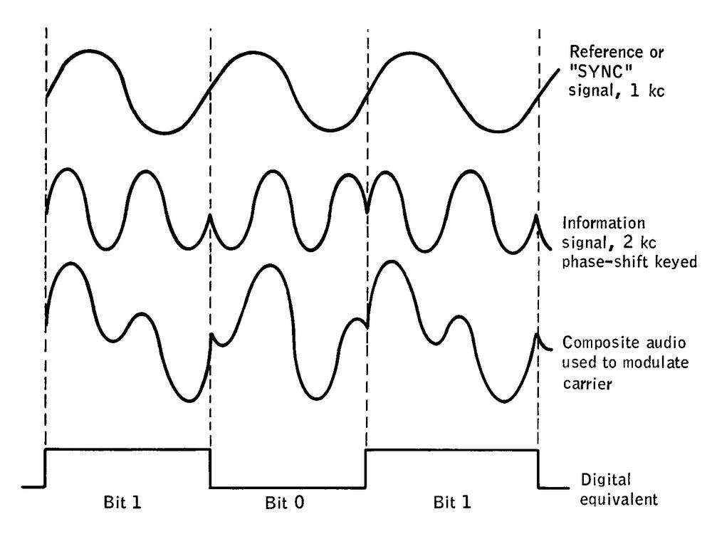
However, some of the box's circuitry was analog, and these modules were harder to decipher, especially the circuitry that encoded the binary output as a phase-shift keying (PSK) signal. Digital data could not be transmitted directly to the spacecraft, but needed to be encoded as an analog waveform for radio transmission. In particular, the digital up-data message was encoded using phase-shift keying (PSK), flipping a 2-kilohertz sine wave to indicate a 0 or a 1. In other words, a phase of 0° indicated a 1 bit while a phase of 180° represented a 0 bit.1

This vintage diagram shows how a binary signal is encoded as an audio signal using phase-shift keying (PSK). "kc" indicataes kilocycles; the unit "Hertz" was made the standard in 1960 but "cycles" remained for years.

This vintage diagram shows how a binary signal is encoded as an audio signal using phase-shift keying (PSK). "kc" indicataes kilocycles; the unit "Hertz" was made the standard in 1960 but "cycles" remained for years.

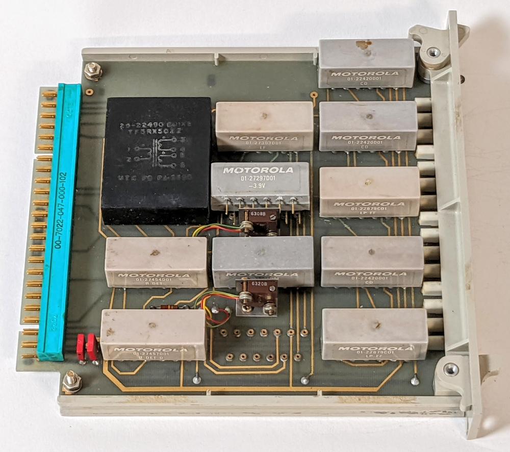
The up-data test box required two boards to perform the PSK modulation and inconveniently a couple of key components (probably high-quality tunable inductors) had been removed when the box was scrapped, making it hard to understand the circuitry. One module sat at the heart of the PSK circuitry, helping to shape the square-wave signals into smooth sine waves. This module had the label "-3.9V" and sure enough it produced -3.9 volts, but it contained additional mysterious circuits (and unexpectedly the -3.9 volt output wasn't used). The mystery circuits appeared to be resistor-capacitor networks. CuriousMarc has a vintage HP resistor-inductor-capacitor meter, capable of measuring series or parallel circuits, but it clicked and flashed its lights unsuccessfully before giving up on the -3.9V module.

The "=3.9V" module is in the center of this board. The module has been removed from the socket to make its label visible. The large black rectangle is a transformer. Selecting a particular winding provides the phase inversion for PSK.

The "=3.9V" module is in the center of this board. The module has been removed from the socket to make its label visible. The large black rectangle is a transformer. Selecting a particular winding provides the phase inversion for PSK.

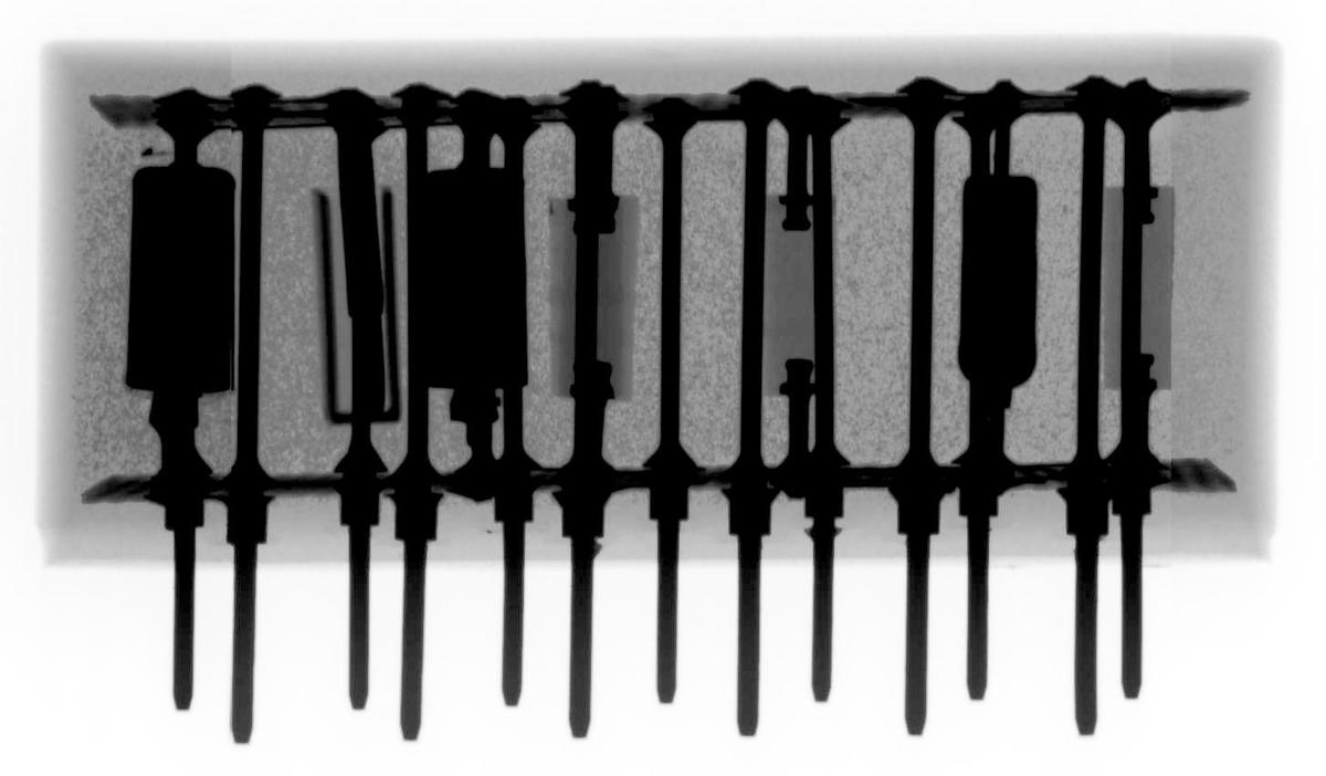
We figured that X-rays might reveal the secrets of the module and John McMaster kindly agreed to X-ray the module. The photo below gives an X-ray view of the module from the side, showing the internal components and the pins at the bottom. The module's plastic packaging is visible as a ghostly gray, not blocking X-rays to the extent of the metal wiring. Two printed-circuit boards are visible, one at the top and one at the bottom, with components mounted vertically, a technique known as cordwood construction. This construction was used in the 1960s when dense packing of components was required, with the cylindrical components stacked together like wooden logs.

X-ray image of the module from the side. Composite of three images.

X-ray image of the module from the side. Composite of three images.

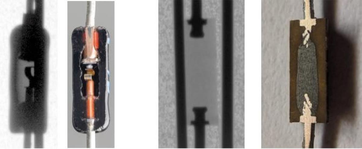
Some of the components have distinctive appearances in their X-ray images. The carbon composition resistors are gray cylinders with leads.2 The Zener diode's internal construction is visible as a ghostly S-shaped spring, as shown below. The opaque cylinders are capacitors, probably with rolled plates blocking the X-rays. The U-shaped rectangular component near the left is a capacitor, probably a metalized film capacitor. The diagram below compares X-ray images and physical cross-sections of Zener diodes and resistors.

X-ray images and cross-sections of Zener diodes and carbon composition resistors. The cross-section components are similar but not identical to the X-ray components. Cross-section photos copyright Eric Schlaepfer and Windell Oskay.

X-ray images and cross-sections of Zener diodes and carbon composition resistors. The cross-section components are similar but not identical to the X-ray components. Cross-section photos copyright Eric Schlaepfer and Windell Oskay.

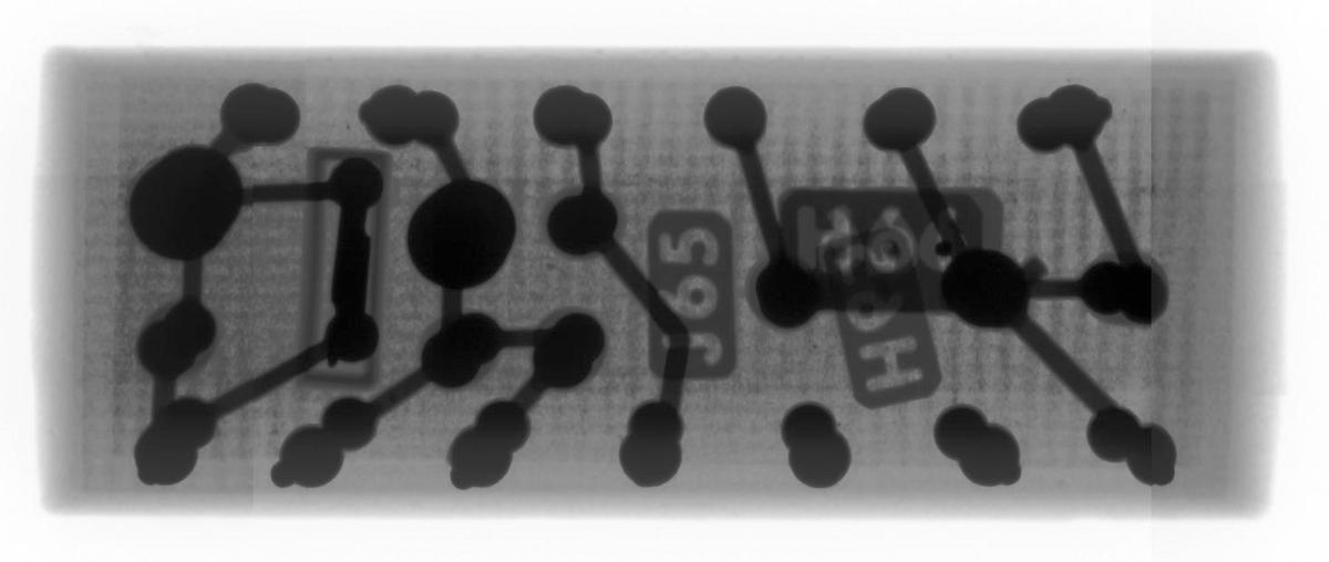
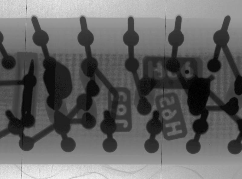
An X-ray image from the bottom of the module provides a different perspective. The pins are at the top and bottom of the image, slightly angled with circles at each end where they are connected to the circuit boards. The cylindrical components show up as circles: larger circles for the capacitors, and smaller circles for the resistors. The important feature of this viewpoint is that it shows the PCB connections between the components, although there is inconvenient ambiguity about whether a trace is on the top or the bottom circuit board. The image also reveals mysterious text such as J65 and H66. These are probably labels etched into the copper of the circuit boards for identification.

X-ray image of the module from the bottom. Composite of three images.

X-ray image of the module from the bottom. Composite of three images.

A tilted view of the module helps to resolve the ambiguity, separating traces on the top circuit board from traces on the bottom circuit board. It still took me some pondering to sort out the internal structure. (A CT scan would figure out the 3-D representation automatically, but this was a regular 2-D X-ray machine.)

Tilted X-ray image of the module.

Tilted X-ray image of the module.

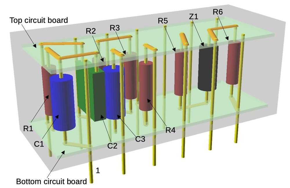
The 3-D model below shows my interpretation of the X-rays images. The module's 13 pins are connected to both the top and bottom circuit boards, as are the cylindrical components. (The square capacitor is an exception, with both connections to the top board.) The traces on the circuit boards create the circuit.

A 3-D representation of the interior of the module, created with OpenSCAD. I don't guarantee that it's 100% accurate.

A 3-D representation of the interior of the module, created with OpenSCAD. I don't guarantee that it's 100% accurate.

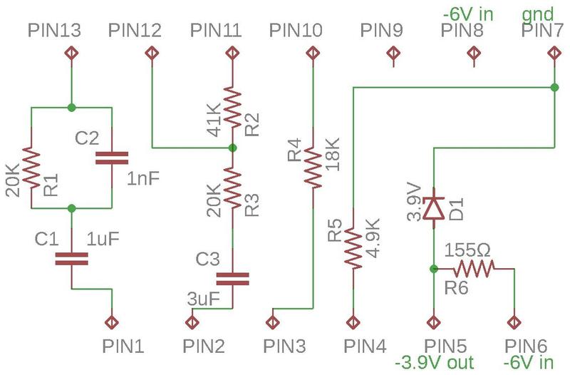
I created the schematic diagram below to match the X-ray images. Prior to the X-rays, we had figured out most of the schematic by probing the module, but there were a few surprises. The most important discovery was the series-parallel structure of R1, C1, and C2, where we had only expected a single resistor and capacitor.3 (This complex topology is why CuriousMarc's Hewlett-Packard device was unable to determine the capacitance.) Another important X-ray observation was that the construction of C2 was different from the other capacitors, so it probably had a very different capacitance, which turned out to be nanofarads vs microfarads. Once I understood the circuit topology, I could probe the circuit with signals of different frequencies and determine the approximate component values.

A schematic diagram of the module. Component values are from curve-fitting to oscilloscope traces, so they're probably off by at least 10%.

A schematic diagram of the module. Component values are from curve-fitting to oscilloscope traces, so they're probably off by at least 10%.

We're still developing a rigorous explanation of the module's function in the box. To summarize, the module helps convert 1-kilohertz and 2-kilohertz square waves into sine waves to produce the PSK output. Through trial and error, CuriousMarc determined the right inductors to make the circuit resonate at these frequencies. The R-C circuits in the module pass a small "kick" when the square wave switches, enough to keep the resonance going, but not so big that it distorts the sine wave. Strangely, the eponymous -3.9V Zener reference isn't used.

Conclusion

The X-ray images cleared up several mysteries about the modules. First, we learned that the modules used cordwood construction, rather than a single PCB or point-to-point wiring. Next, the X-rays revealed a couple of unexpected components and helped us figure out the circuit technology. Finally, we could see the internal structure of some components, which we weren't expecting to be visible. The main lesson I learned for future X-rays is to take shots from multiple angles to help resolve 3-D ambiguities.

I'm curious about whether these Motorola modules were part of a comprehensive prototyping product. We've looked at a lot of Apollo hardware and have never seen these modules elsewhere. I haven't been able to find any reference to them. The construction seems like a flexible system designed for prototyping; the modules, the circuit boards, the plastic frames to hold them, the connectors, and the chassis all seem designed to work together. It gives the impression of a well-thought-out system for building electronic hardware in the 1960s, but apparently it vanished without a trace (except for this box). If any readers know more about these modules, please let me know.

As for the -3.9V module specifically, what was the original purpose of this module and why did the designers use it in the up-data test box? I can understand selling logic gates and flip flops as generic components, but this module seems much too specialized to be a standard product. On the other hand, a custom module would just require new PCBs—a small investment compared to designing a new integrated circuit—so producing custom modules seems very practical. But that raises the question of why they would custom-design a -3.9 volt module for the up-data test box and then not use its Zener circuit. My current hypothesis is that the -3.9 volt module was designed for an earlier revision of the up-data test box but that functionality turned out to be not used.

If you want more background on the Up-data Test Box, I have some Twitter threads: power-up, modules, paper tape reader, and clock circuit. Also see CuriousMarc's video on the box:

We plan to connect the up-data test box to the up-data link box and see if they work together. Then, we hope to create the full signal path: the up-data test box to a transmitter, and then the S-band transponder to the up-data link box, so we can transmit messages via radio (albeit over a few feet rather than to the Moon). I announce my latest blog posts on Twitter, so follow me @kenshirriff for updates. I also have an RSS feed. Many thanks to John McMaster for X-raying the module and to Marcel for providing the up-data test box. Cross-section photos courtesy of Windell Oskay and Eric Schlaepfer, from the upcoming book Open Circuits, which you should check out.

Notes and references

  1. Phase-shift keying was just the beginning of the signal's processing on the way to the spacecraft. Next, the PSK signal was modulated on a 70-kilohertz subcarrier (so it wouldn't conflict with the voice transmission), and finally phase-modulated at exactly 2106.40625 megahertz for transmission from a massive ground antenna to the distant spacecraft. 

  2. In the X-rays, some of the resistors look like they have a solid connection through the resistor (which would short them out). This is just a coincidental alignment of a module pin with the resistor in the image. 

  3. The other unexpected feature we uncovered from the X-rays was resistor R6. During probing, I had also missed the presence of R6, since it was not used by this board. 

Talking with the Moon: Inside Apollo's premodulation processor

The Apollo missions to the Moon required complex hardware to communicate between Earth and the spacecraft, sending radio signals over hundreds of thousands of miles. The premodulation processor was a key component of this system, combining voice, scientific data, TV, and telemetry for transmission to Earth.1 It was built from components that were welded together and tightly packed into a 14.5-pound box.2 In this blog post, I look inside the premodulation processor, examine its construction, and describe how each module worked.

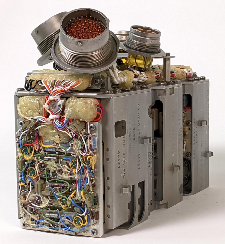
The premodulation processor with its case removed, showing some of the circuitry. (Click any image for a larger version.)

The premodulation processor with its case removed, showing some of the circuitry. (Click any image for a larger version.)

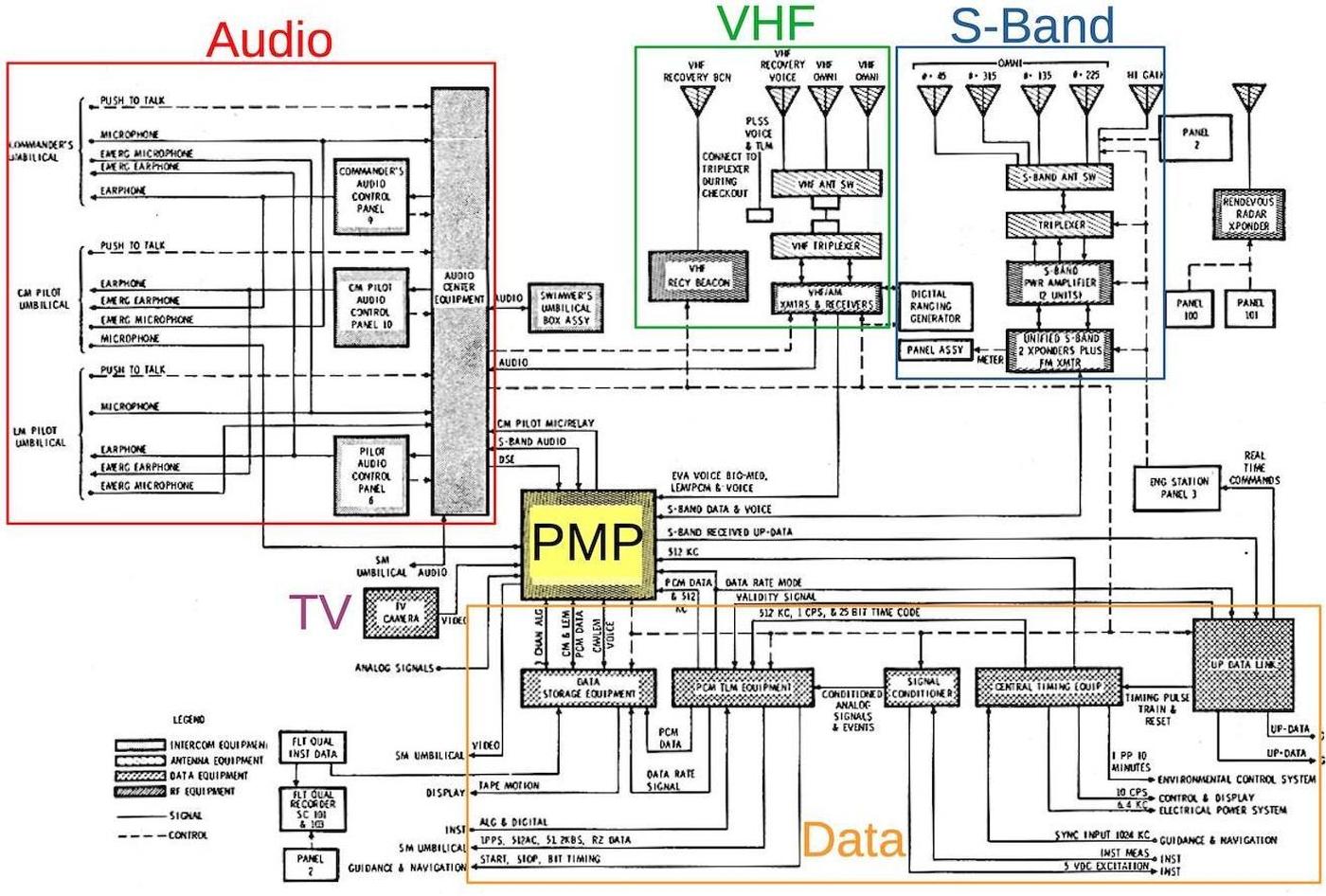
The communications systems in the Apollo Command Module were very complex, as shown in the block diagram below.3 The premodulation processor (PMP, yellow) played a central role: most of the audio (red), data (orange), and TV (purple) went through the premodulation processor, where the signals were combined for transmission by the S-band (blue) radio systems. The premodulation processor also handled most of the voice and data signals received from Earth or from the Lunar Module via the VHF (green) or S-band radio systems.

Block diagram of the Apollo communications system.
From Apollo Operations Handbook: Telecommunications System page 3.

Block diagram of the Apollo communications system. From Apollo Operations Handbook: Telecommunications System page 3.

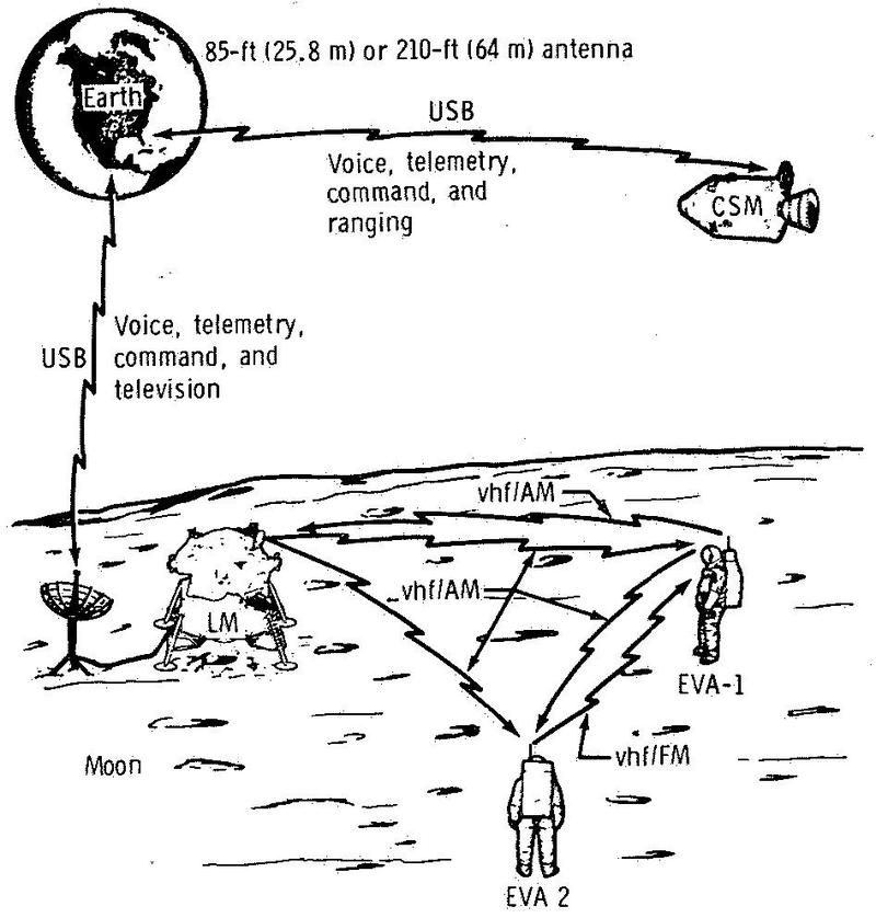
One reason for the complexity of the premodulation processor was that the audio system had to support a variety of communications configurations. The diagram below illustrates one configuration, when astronauts were walking on the Moon (i.e. extra-vehicular activity, EVA). They communicated with the Lunar Module on the Moon's surface via VHF/AM radio, which relayed their audio to Earth via the Unified S-Band (USB) radio. Meanwhile, the Command and Service Module (CSM) orbiting the Moon also communicated with Earth via S-Band. These voices were conferenced together so the astronauts and ground could all hear each other. The need for redundancy added to the complexity; for example, signals from the Moon could be relayed through the Command Module in the event of an equipment failure.

Typical Apollo communication for lunar surface operations. From Apollo Experience Report.

Typical Apollo communication for lunar surface operations. From Apollo Experience Report.

Construction

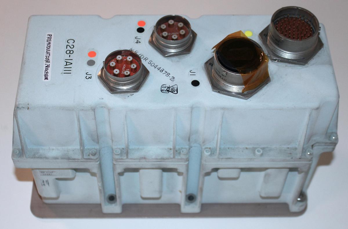
Like much of the Apollo electronics, the premodulation processor was packaged in a drab bluish metal case. The case has four round military-style connectors on top that linked the various audio, RF, and control signals to other components of the spacecraft.

This photo shows the premodulation processor inside its case.

This photo shows the premodulation processor inside its case.

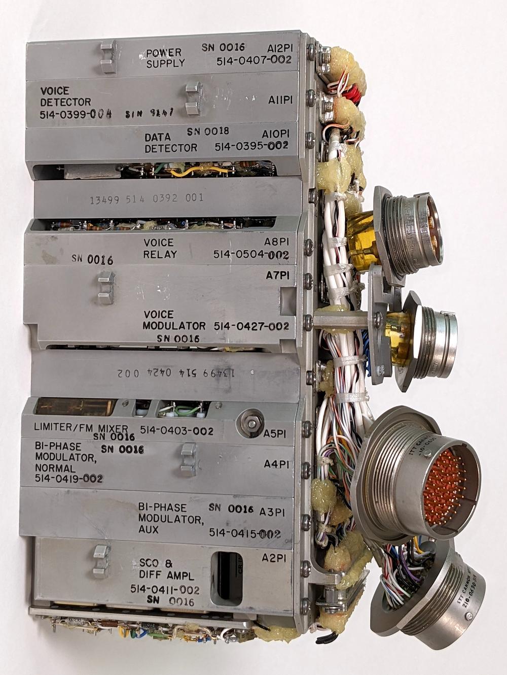
We opened the case by removing the screws and inside we found 11 rectangular modules packed together tightly, from the power supply at the top to the "SCO & diff ampl" (subcarrier oscillator and differential amplifier) at the bottom, conveniently labeled with their functions. The modules were plugged into a thin backplane,5 at the right, connected by D-Sub connectors, similar to vintage RS-232 connectors but in a variety of sizes. Bundles of wires connected the backplane to the round connectors. This construction technique made it easy for us to remove the modules and inspect them individually.

A side view of the premodulation processor, showing the labeled modules.

A side view of the premodulation processor, showing the labeled modules.

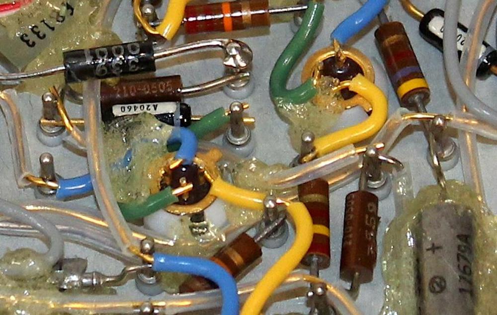
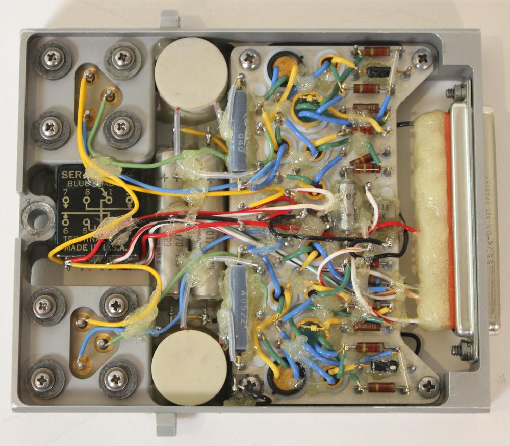
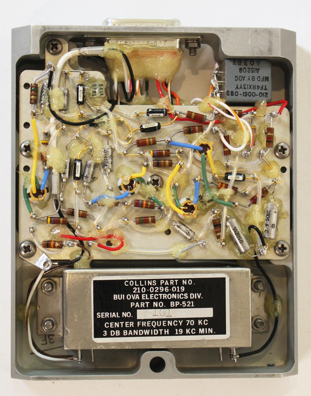
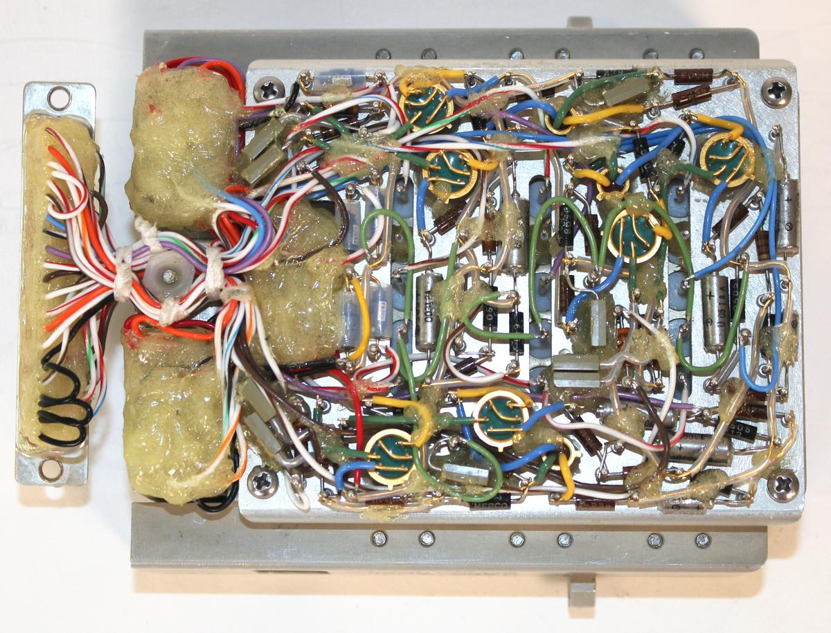
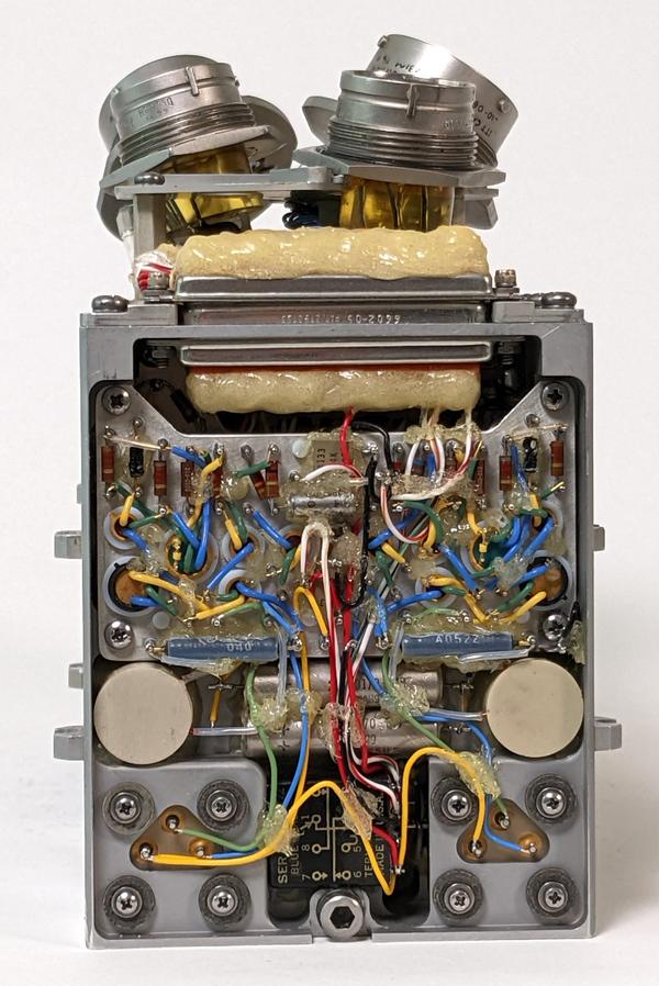
The modules themselves don't use printed-circuit boards, but instead are built from components that are spot-welded to metal pegs, as shown below.6 These resistors, diodes, capacitors, and transistors are tightly packed with a jumble of overlapping wiring. Most of the wiring consists of the component leads, but point-to-point wiring provided additional connection. The wiring is a combination of color-coded insulated wires, bare wires, and bare wires in clear insulating tubes. The components are liberally covered in what looks like hot glue. I suspect that the hot glue was only used in equipment for ground testing, while modules for spaceflight were fully encapsulated to prevent short circuits.

A closeup of the wiring in the aux bi-phase modulator module. Most of the connections are spot-welded, although a few seem to have solder.

A closeup of the wiring in the aux bi-phase modulator module. Most of the connections are spot-welded, although a few seem to have solder.

The modules have circuitry on both sides, which increased the density. About half of the metal pegs provide connection to the other side, while half have plastic stubs on one side. As will be seen below, many of the modules also contain rectangular metal sub-units that implement functional blocks such as oscillators or filters. It appears that these standardized functions could be bought "off-the-shelf", not as integrated circuits, but as blocks containing discrete components.

In the following sections, I'll discuss each module in more detail, starting with the power supply.

Power supply module

The premodulation processor contains a power supply that converted the spacecraft's 28-volt DC supply to 18 volts. For efficiency, it is a switching power supply, a buck converter that chops up the input power at a high frequency to drop it to the lower voltage. Although switching power supplies are now ubiquitous, in everything from phone chargers to PC power supplies, switching power supplies were expensive and rare in the 1960s, used in aerospace applications that required a compact, high-efficiency power supply.

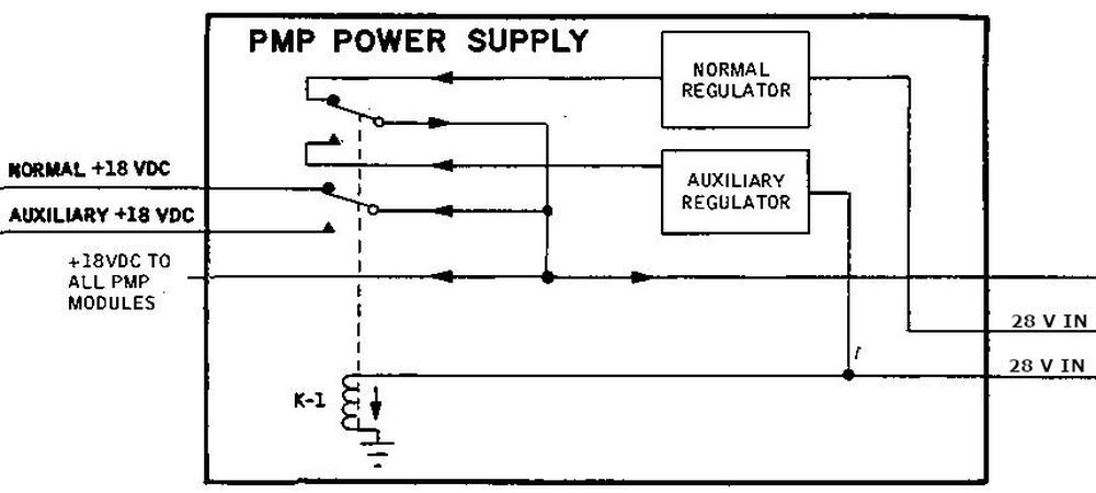
The block diagram below shows that the power supply was implemented redundantly, with a normal regular and an auxiliary regulator. A relay switches between the two regulators, controlled by the PMP NORM/AUX switch.

Diagram of the power supply module. From Command/Service Module Systems Handbook p63.

Diagram of the power supply module. From Command/Service Module Systems Handbook p63.

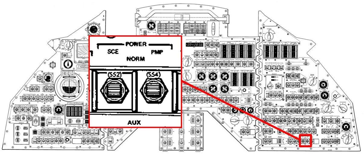
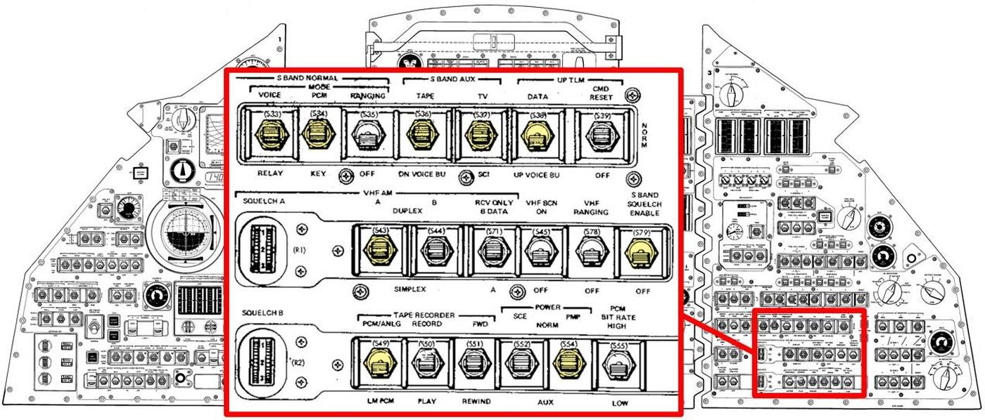
You may know of the Apollo 12 incident where the spacecraft was hit by lightning seconds after launch, scrambling the telemetry. The problem was resolved by the famous "set SCE to AUX" switch.7 The PMP's power switch is next to the SCE switch but never played a dramatic role.8

The power switches for the signal conditioning equipment (SCE) and the premodulation processor (PMP) are in the lower-left corner of the Command Module's control panel. Each switch has positions for NORM, OFF, and AUX.

The power switches for the signal conditioning equipment (SCE) and the premodulation processor (PMP) are in the lower-left corner of the Command Module's control panel. Each switch has positions for NORM, OFF, and AUX.

The photo below shows the power supply module. The redundant halves of the power supply are visible with the lower circuitry a mirror image of the upper circuitry. The relay to switch between the two is the black box in the center-left. The power switching transistors are above and below the relay, fastened down with screws. To the right of the transistors are cylindrical tan inductors, storing energy across each pulse. Large silver filter capacitors are between the inductors. The right half of the module is the control circuitry: resistors, capacitors, transistors, and diodes. The connector at the far right connects the power supply to the other modules via the backplane.

The power supply module for the premodulation processor.

The power supply module for the premodulation processor.

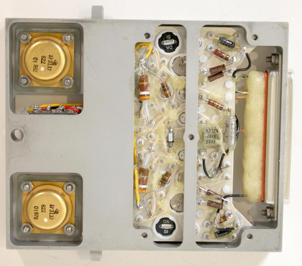
Flipping the power supply over reveals the high-frequency power transistors, in large metal packages to dissipate heat. These packages are square, unlike the typical two-tab (TO-3) power transistor packaging. Note the second layer of discrete component circuitry on this side of the module. This illustrates how the modules have two layers of circuitry, one on each side. You can also see the tops of the smaller transistors that are wired on the other side.

Underside of the power supply with 2N3137 power transistors.

Underside of the power supply with 2N3137 power transistors.

Voice and data detector module

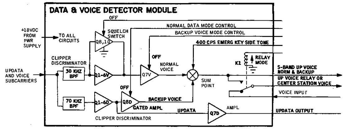
The data and voice detectors handle signals transmitted to the spacecraft over the S-band. The S-band transceiver receives these signals, demodulates them, and passes the signal to the premodulation processor. The data and voice detectors appear as one module on the block diagram below but are implemented as two modules physically.

Diagram of the data and voice detector modules. From Command/Service Module Systems Handbook p63.

Diagram of the data and voice detector modules. From Command/Service Module Systems Handbook p63.

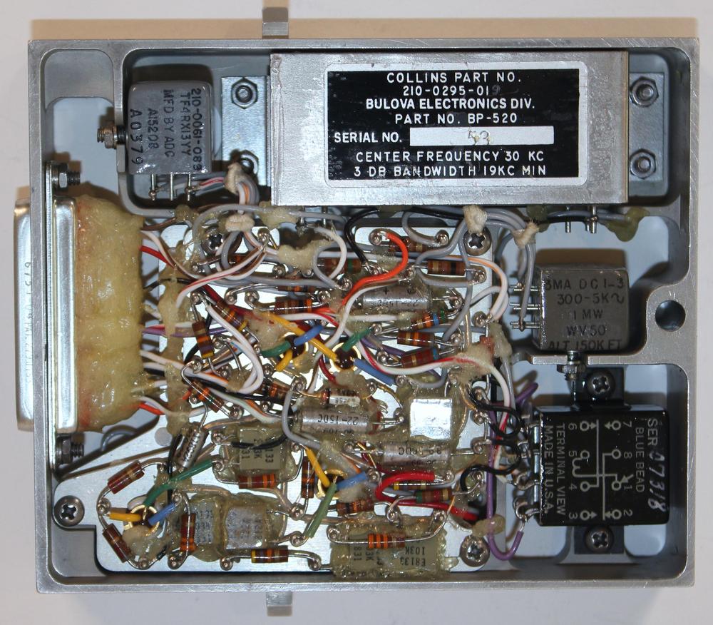
The photo below shows the voice detector module. Voice is transmitted to the spacecraft, frequency modulated onto a 30-kilohertz subcarrier. The voice detector extracts this signal through a 30-kilohertz bandpass filter, demodulates it with an FM discriminator, amplifies it, and sends it to the Audio Center, which provides it to the astronauts. The largest component of the module is the 30-kilohertz bandpass filter at the center top. This module was built by Bulova Electronics, a division of the watch company that produced quartz crystals, oscillators, filters, servo amplifiers, and other components. Two gray transformers are also visible; these coupled the audio signals. The black relay in the lower right was controlled by the "Up Voice Relay" console switch. (Don't be confused by the two completely different definitions of "relay".)

The circuitry of the voice detector module. The connector is on the left.

The circuitry of the voice detector module. The connector is on the left.

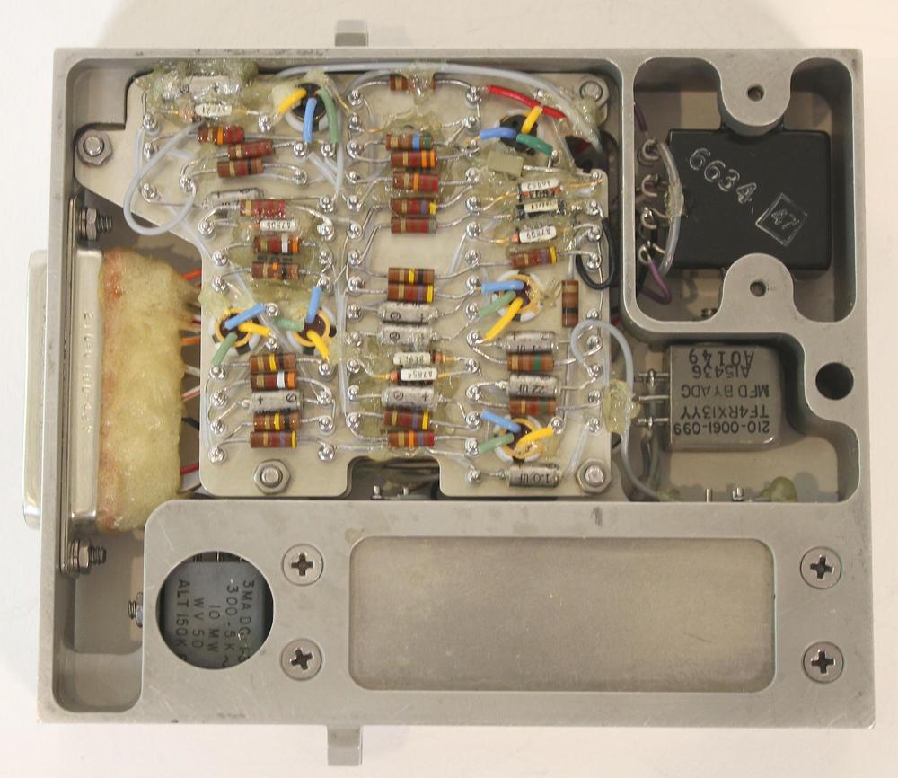
More circuitry is on the other side of the voice detector. The transformers, relay, and bandpass filter are visible through openings in the module's metal frame. The discrete components are arranged in orderly columns, unlike the other modules.

The other side of the voice detector module.

The other side of the voice detector module.

The data detector module operated similarly to the voice detector, except that it extracted the data link signals from ground. From the data detector module, data was processed by the Up-Data Link box, giving the ground control over multiple spacecraft systems. For instance, commands could be entered into the Apollo Guidance Computer. The spacecraft clock (CTE, Central Timing Equipment) could be set. Various relays could be controlled, overriding some of the switches on the console.

The data detector module. It contains a 70-kilohertz bandpass filter produced by Bulova.

The data detector module. It contains a 70-kilohertz bandpass filter produced by Bulova.

The implementation of the data detector module (above) is similar to the voice detector module, but simpler since it doesn't have the summing and switching circuitry. It uses a 70-kilohertz bandpass filter module, rather than the voice detector's 30-kilohertz filter. In case of a malfunction with the voice detector, backup voice communication could be transmitted to the spacecraft over the 70-kilohertz subcarrier, and extracted by the data detector module. This mode was controlled by the "Up-voice backup" switch.

Bi-phase modulator modules

The role of the bi-phase modulator modules was to modulate telemetry data using bi-phase modulation. In total, data had three layers of modulation. First, data was digitally encoded using pulse-code modulation (PCM). Next, this module applied bi-phase modulation to the bits at 1.024 MHz. Finally, the S-band transceiver used FM or PM (frequency or phase modulation) for the communication to Earth.

Bi-phase modulation encodes a bit using a sine wave for a 1 and an inverted sine wave for a 0 (i.e. a phase shift of 180°). Bi-phase modulation is a type of phase-shift keying. The PCM data was at 51.2 kilobits per second ("high bit rate") or 1.6 kilobits per second ("low bit rate"). Since the data was modulated at 1.024 MHz, a bit was encoded by at least 20 cycles of the waveform. This gave the receiver plenty of time to determine the phase and distinguish a 0 from a 1.

Diagram of the normal bi-phase module. From Command/Service Module Systems Handbook p63.

Diagram of the normal bi-phase module. From Command/Service Module Systems Handbook p63.

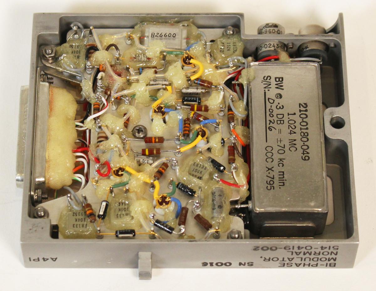
The premoduation processor contains two modulator modules: the "normal" module and the "auxiliary" module. The normal module transmits real-time data over PM, while the auxiliary module is more flexible. The normal bi-phase modulator module (below) contains a complex tangle of circuitry. The 1.024 MHz bandpass filter is the large metal package at the right, limiting the output signal to a narrow frequency range around 1.024 Mhz.

Inside the bi-phase modulator module.

Inside the bi-phase modulator module.

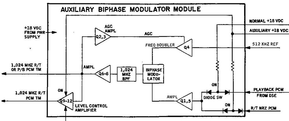
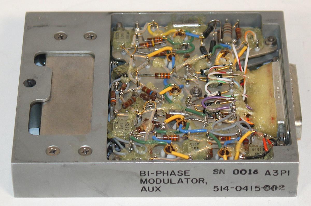
The auxiliary bi-phase modulator (below) is roughly the same as the normal modulator, but with a bit more circuitry to switch between modes, transmitting either recorded PCM data from tape or real-time PCM data, using the PM or FM transmitters. Curiously, the different modes are selected by switching the power supply between NORM and AUX. In NORM mode, the auxiliary module transmits recorded data over FM. In AUX mode, the auxiliary module transmits real-time data over both PM and FM, providing a backup in case the normal module fails.

Diagram of the auxiliary bi-phase module. From Command/Service Module Systems Handbook p63.

Diagram of the auxiliary bi-phase module. From Command/Service Module Systems Handbook p63.

The output signals from the bi-phase modulators are processed either by the FM mixer / LM PCM limiter module or the PM mixer / key / TV module; these are discussed later.

Underside of the auxiliary bi-phase modulator. The bandpass filter is at the left.

Underside of the auxiliary bi-phase modulator. The bandpass filter is at the left.

Voice clipper module

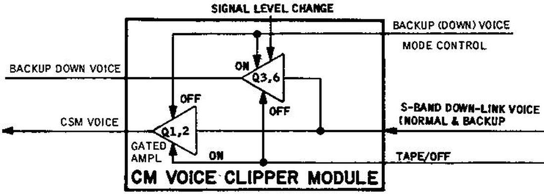
Voice communication from astronauts to the ground ("downlink voice") went through multiple stages of processing to improve quality. The design standard for the Apollo audio system was 90% word intelligibility for the main links and 70% for the backup links.9 This standard seems surprisingly poor, with one out of 10 words unintelligible, but achieving this standard was challenging due to the extreme distance to the Moon. Moreover, the spacecraft had a lot of ambient noise that interfered with communication. To maximize voice intelligibility over the available radio link, the voice signal was pre-emphasized and clipped. The voice clipper module (below) implemented the pre-emphasis and clipping of the voice signal.

Diagram of the voice clipper module. From Command/Service Module Systems Handbook p63.

Diagram of the voice clipper module. From Command/Service Module Systems Handbook p63.

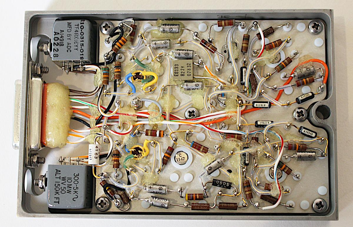
The photo below shows the voice clipper module. It has two gray audio transformers at the left. The remainder of the module is filled with circuitry.

The voice clipper module.

The voice clipper module.

The voice signal next goes to the voice relay module, discussed below. (The backup voice signal, however, went directly to the S-band transceiver for transmission to ground.)10

Voice relay module

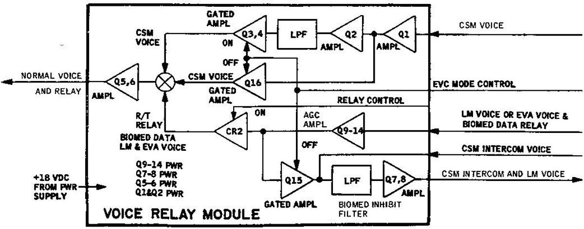
The voice relay module permitted voice communication from the Lunar Module to be relayed through the Command Module instead of being transmitted directly to Earth from the Lunar Module. If the S-band mode switch was set to "RELAY", the voice and biomedical data from the Lunar Module would be mixed in with the Command Module's voice signal and sent to Earth. This module also optionally applied a low-pass filter to the Command Module's voice signal, under the control of the VHF duplex switch. (I think this is so voice and biomed data can be sent over the same channel without frequency conflict.)

Diagram of the voice relay module. From Command/Service Module Systems Handbook p63.

Diagram of the voice relay module. From Command/Service Module Systems Handbook p63.

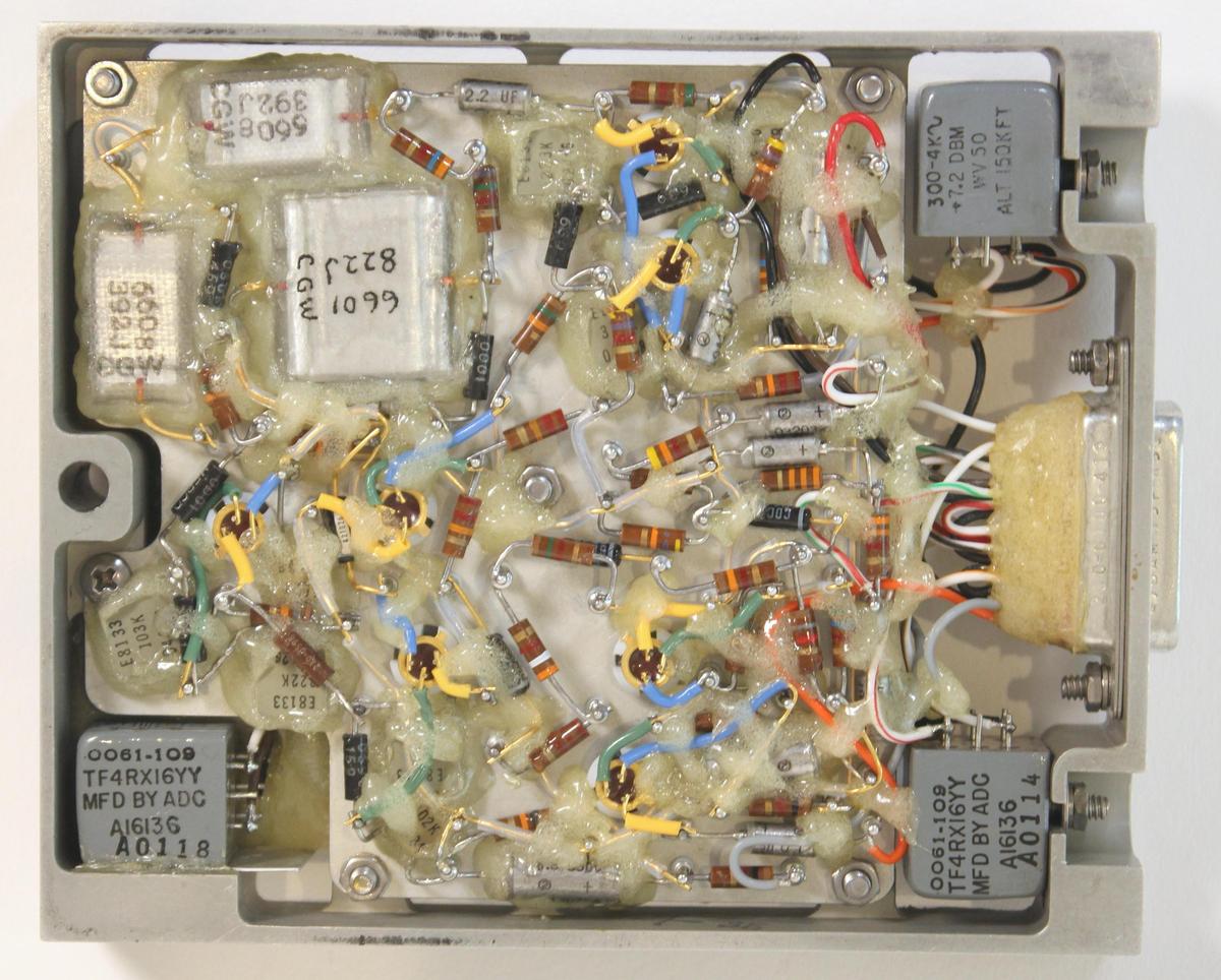
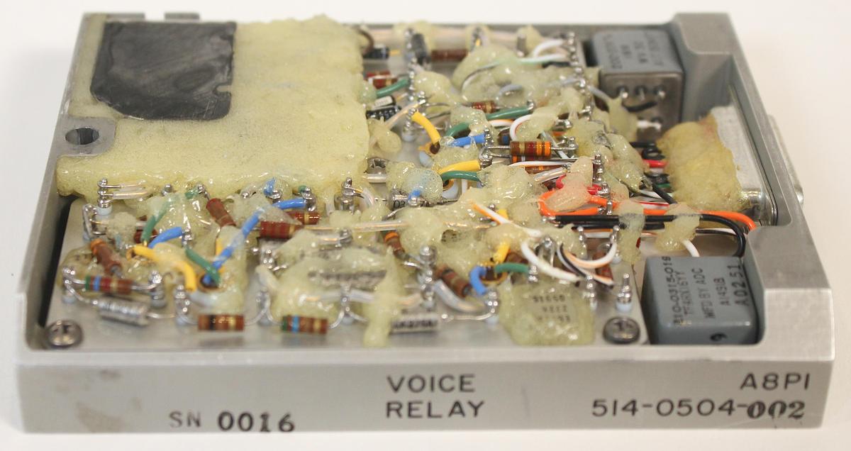
The photo below shows the voice relay module circuitry. There are three audio transformers, along with circuitry liberally encased in goo.

The voice relay module.

The voice relay module.

Flipping the module over, the upper right corner is completely covered in plastic. The reason for this is unclear. That corner holds one of the transformers, but I don't see a reason why this one in particular would be covered.

The other side of the voice relay module.

The other side of the voice relay module.

Voice modulator module

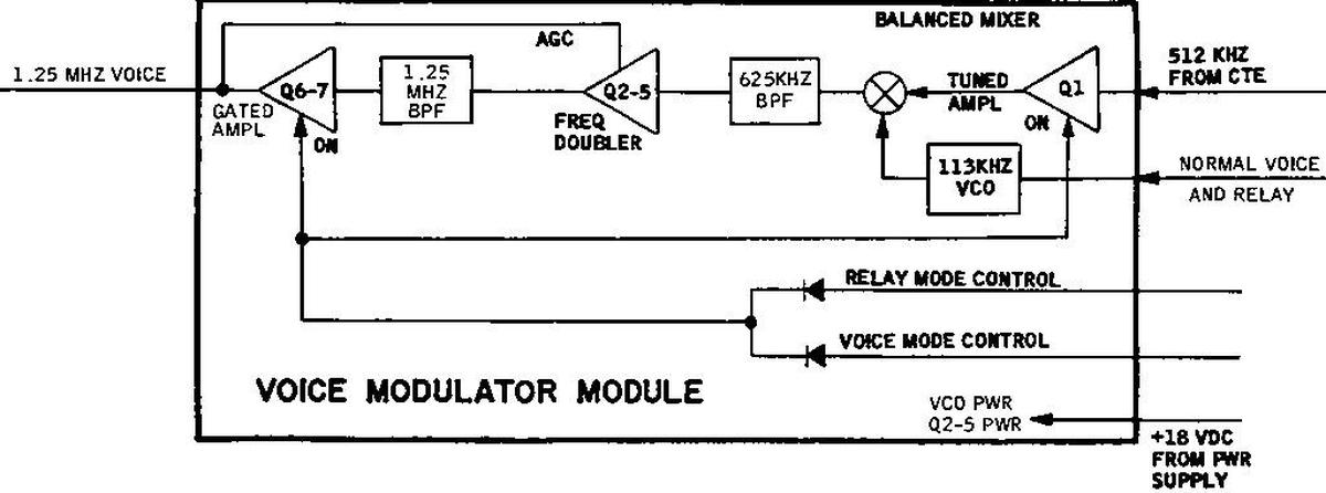
Next, the voice signal went to the voice modulator module, which used a complicated circuit to apply frequency modulation. First, the voice signal controls a 113-kilohertz voltage-controlled oscillator (VCO), yielding an FM signal at 113 kilohertz. Next, this signal is mixed with a 512-kilohertz signal from the central timing equipment (CTE), yielding signals at the sum and difference frequencies (399 kHz and 625 kHz). The bandpass filter passes the 625-kilohertz FM signal. The signal frequency is doubled and filtered to produce the final 1.25 MHz FM signal.

Diagram of the voice modulator module. From Command/Service Module Systems Handbook p63.

Diagram of the voice modulator module. From Command/Service Module Systems Handbook p63.

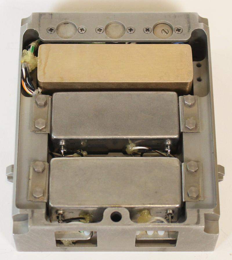
Three large modules are visible inside: the voltage-controlled oscillator and the two bandpass filters.

Inside the voice modulator module.

Inside the voice modulator module.

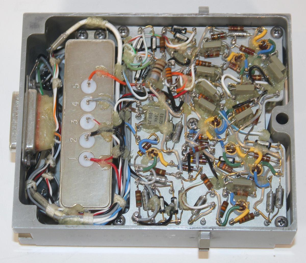
The other side of the module has the circuitry, wired to the larger modules. The frequency-doubler may be implemented by a varactor diode, but I haven't located it. From the voice modulator, the voice signal passed to the PM mixer / key / TV module.

Another view of the voice modulator module.

Another view of the voice modulator module.

PM mixer/key/TV module

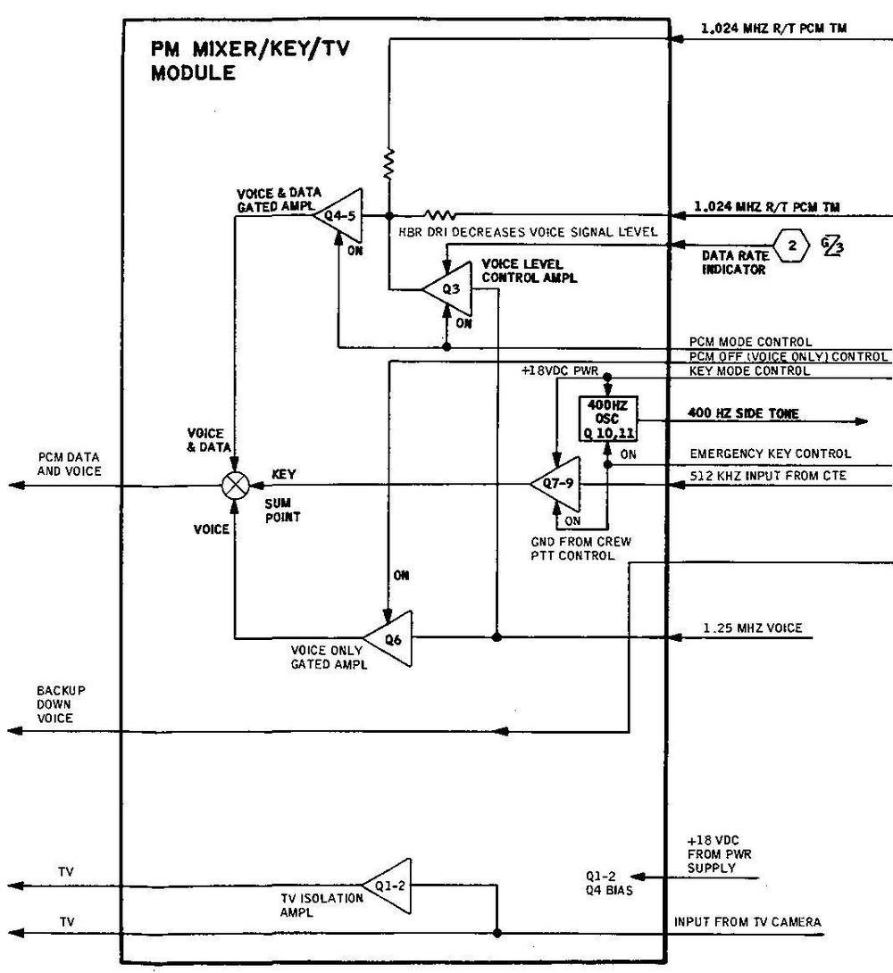
As the name suggests, the PM mixer/key/TV module had multiple functions. In the top part of the diagram below, the mixer combines three data sources: voice with data, emergency keying, and voice. The voice and data combination consists of PCM data at 1.024 megahertz with voice data at 1.25 megahertz; the PCM data is provided by one of the bi-phase modulator modules, while the voice data is provided by the voice modulator module. The next mixer input is the emergency key signal. The purpose of emergency key is that if voice communication failed, an astronaut could send Morse code by using the XMIT key on their communication cable. This key signal might be able to get through to Earth even if voice communication fails or is unintelligible. This module produces the emergency key signal at 512 kHz along with a 400 Hz feedback tone for the astronauts. The final mixer source is voice. The sum of these signals is sent to the S-band PM transponder for phase modulation and transmission. This module also includes a TV isolation amplifier to supply a TV signal to ground support equipment (GSE) before launch.

Diagram of the PM mixer / key / TV module. From Command/Service Module Systems Handbook p63.

Diagram of the PM mixer / key / TV module. From Command/Service Module Systems Handbook p63.

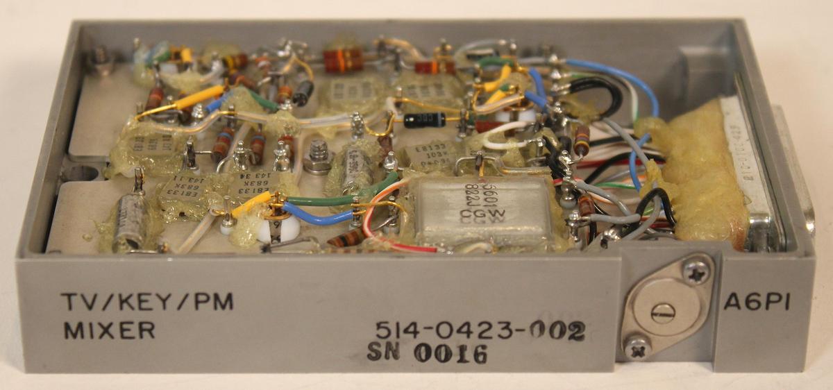
The photo below shows this module. On the front right is a component that looks a bit like a power transistor. However, it is an adjustable component (note the screw in the middle), probably a variable resistor.

The PM mixer / key / TV module.

The PM mixer / key / TV module.

SCO (subcarrier oscillator) and differential amplifier

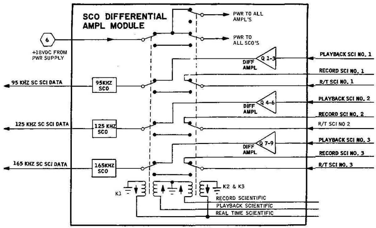
This module is used for transmitting three channels of analog scientific data. (This is in contrast to most of the data, which was transmitted digitally, using pulse-code modulation (PCM).) Each of the three scientific signals modulates a subcarrier oscillator on a different frequency: 95 kHz, 125 kHz, and 165 kHz. These signals are sent to the FM mixer / LM PCM limiter module, which will be discussed in the next section.

This module also contains relays so the real-time scientific data could be directed to tape for storage. The recorded data could be played back for transmission, amplified by the differential amplifiers. The mode was controlled by the S-band Aux TV/SCI switch. If set to SCI, real-time scientific data was transmitted. If the transmitter was used for TV, the scientific data was recorded to tape for later playback. The tape recorder switch was set to PCM/ANLG to play back the analog data.

Diagram of the SCO differential amplifier module. From Command/Service Module Systems Handbook p63.

Diagram of the SCO differential amplifier module. From Command/Service Module Systems Handbook p63.

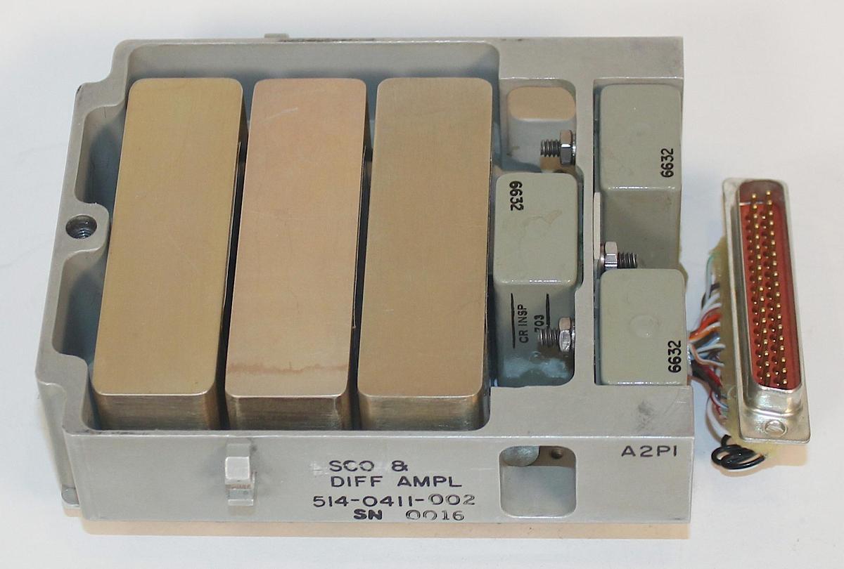
Inside, the three large tan oscillator modules are visible. The three relays are the smaller grayish boxes. This module has the D-Sub connector attached with wires and rotated 90°, unlike the other modules that have the connector mounted to the end of the module.

The SCO & differential amplifier module.

The SCO & differential amplifier module.

On the other side of the module, the circuitry is visible. Note the 6-pin transistors (gold and green circles). These probably contain two carefully-matched transistors for the differential amplifiers. The performance of a differential amplifier strongly depends on its two input transistors; by putting the transistors in the same package, the effects of temperature are minimized.

Another view of the SCO & differential amplifier module.

Another view of the SCO & differential amplifier module.

FM mixer / LM PCM limiter module

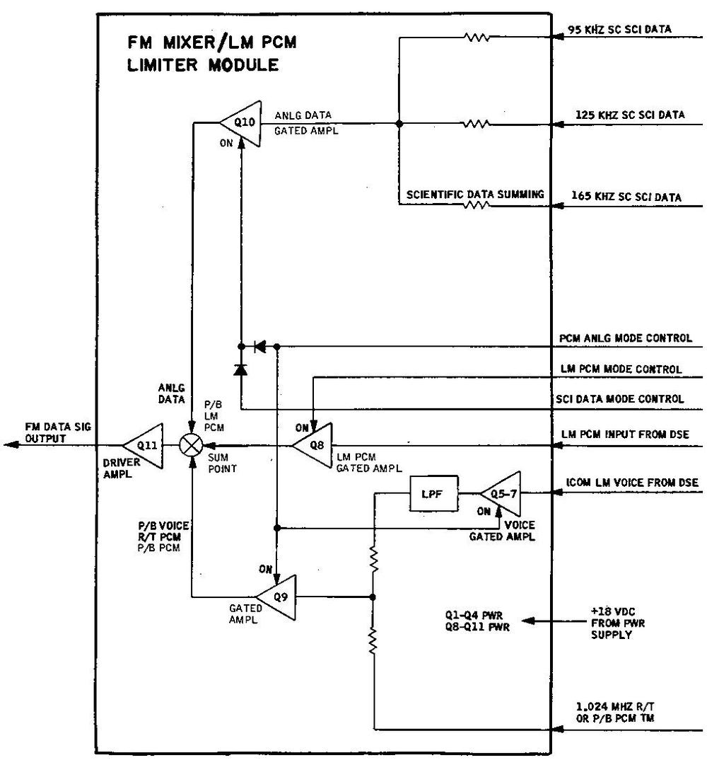
The final module is the FM mixer / LM PCM limiter. Like the PM mixer module, this module combines multiple signals for transmission. But this module prepares signals for FM transmission rather than PM transmission. Specifically, the module combines the three analog scientific data inputs, digital PCM data from the Lunar Module, intercom voice from the Lunar module, and PCM data modulated at 1.024 MHz. Various switches on the console control the different modes.

Diagram of the FM mixer / LM PCM limiter module. From Command/Service Module Systems Handbook p63.

Diagram of the FM mixer / LM PCM limiter module. From Command/Service Module Systems Handbook p63.

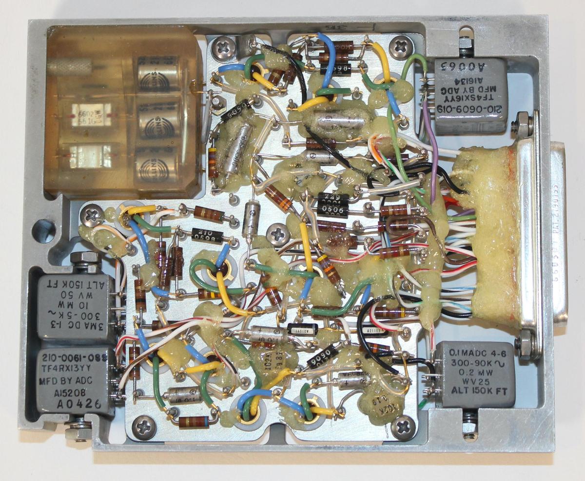
The photo below shows the module's circuitry. It has four gray transformers along with the typical transistors, diodes, resistors, and capacitors.

The FM mixer / LM PCM limiter module.

The FM mixer / LM PCM limiter module.

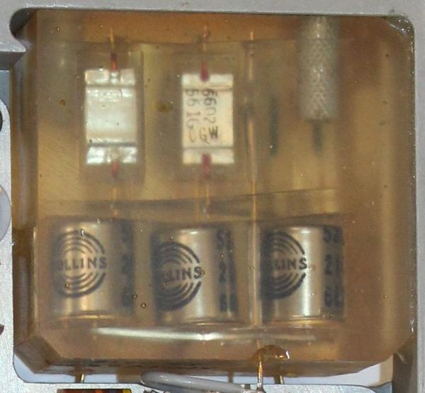
The unusual feature of this module is the encapsulated module in the upper left. This module appears to contain three transistors and five capacitors. It's unclear why these components are encased in plastic. The block diagram for this module doesn't show any special circuitry that would motivate encapsulation. I hope to reverse-engineer this module to figure this out.

The encapsulated block appears to contain three transistors and five capacitors.

The encapsulated block appears to contain three transistors and five capacitors.

Conclusion

Well, I had planned to write a quick description of what we saw inside the premodulation processor but it turned out to be much more complicated than I expected. Congratulations on making it to the end of this blog post.

The premodulation processor illustrates how analog electronics were very bulky before integrated circuits became popular. In the modules, amplifiers and other functional blocks were built from discrete components. The result was a 14.5-pound box to perform a few signal processing tasks. A decade later, many of the circuits could have been replaced with compact ICs.

The premodulation processor also shows how complex everything was in Apollo. You might think that transmitting voice, data, and TV wouldn't be too tricky, just three signals. But everything needed to be redundant. Then there were special cases, such as recording data when you're on the far side of the Moon. Or communicating between astronauts in the Command Module, in the Lunar Module, and walking on the Moon. All these cases required circuitry to switch signals and optimize the radio link for each mode. And the premodulation processor is just one of many boxes in the Apollo communications system! Apollo is like a fractal, where you find successive layers of complexity as you look closer at any system.

We haven't been able to find detailed schematics of the premodulation processor modules, so I plan to reverse-engineer some of the circuitry. I announce my latest blog posts on Twitter, so follow me @kenshirriff for updates. I also have an RSS feed. Thanks to Marcel for providing the premodulation processor and letting Mike, CuriousMarc and me disassemble it.

Front view of the premodulation processor with the case removed.

Front view of the premodulation processor with the case removed.

Notes and references

  1. The Apollo Operations Handbook: Telecommunications System gives this description: "The premodulation processor (PMP) equipment provides the interface connection between the airborne data-gathering equipment and the RF electronics. The PMP accomplishes signal modulation and demodulation, signal mixing, and the proper switching of signals so that the correct intelligence corresponding to a given mode of operation is transmitted." 

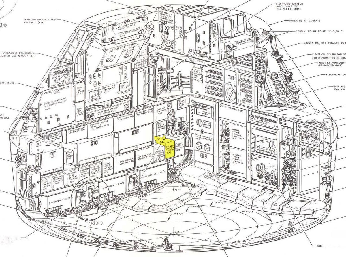
  2. The premodulation processor was one of many boxes of electronic circuitry packed into the spacecraft and linked by thick cables. The diagram below highlights where it was mounted in the lower equipment bay of the Apollo Command Module.

    The premodulation processor was one of many electronic boxes in the Command Module's lower equipment bay. Diagram from Command/Service Module Systems Handbook p212.

    The premodulation processor was one of many electronic boxes in the Command Module's lower equipment bay. Diagram from Command/Service Module Systems Handbook p212.


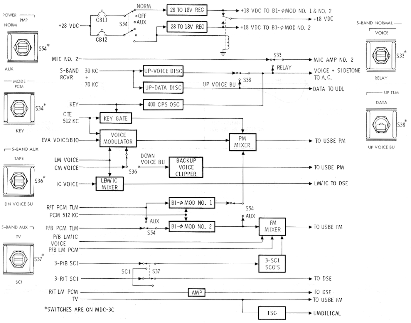
  3. The block diagram below shows the functions of the premodulation processor, along with the switches that control it.

    A block diagram of the premodulation processor. From Apollo Operations Handbook: Telecommunications System.

    A block diagram of the premodulation processor. From Apollo Operations Handbook: Telecommunications System.

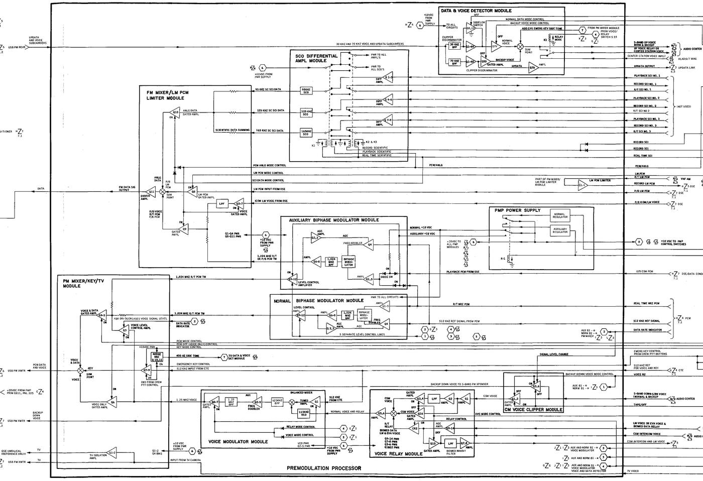
    The block diagram below provides a more detailed view of the premodulation processor. I split out the sub-module diagrams for the discussion, but the full diagram shows the interconnections between the modules.

    Block diagram of the PMP. (Click for a larger version.)
From Command/Service Module Systems Handbook p63.

    Block diagram of the PMP. (Click for a larger version.) From Command/Service Module Systems Handbook p63.


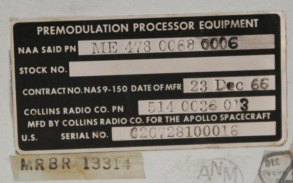
  4. As shown by the nameplate, the premodulation processor was built by Collins Radio in 1966, two days before Christmas. Collins Radio built much of the communications equipment for the space program from Mercury through Apollo including the Deep Space Network antenna system, microwave links, and ground support equipment (details).4

    The nameplate for the premodulation processor shows that it was built by Collins Radio.

    The nameplate for the premodulation processor shows that it was built by Collins Radio.


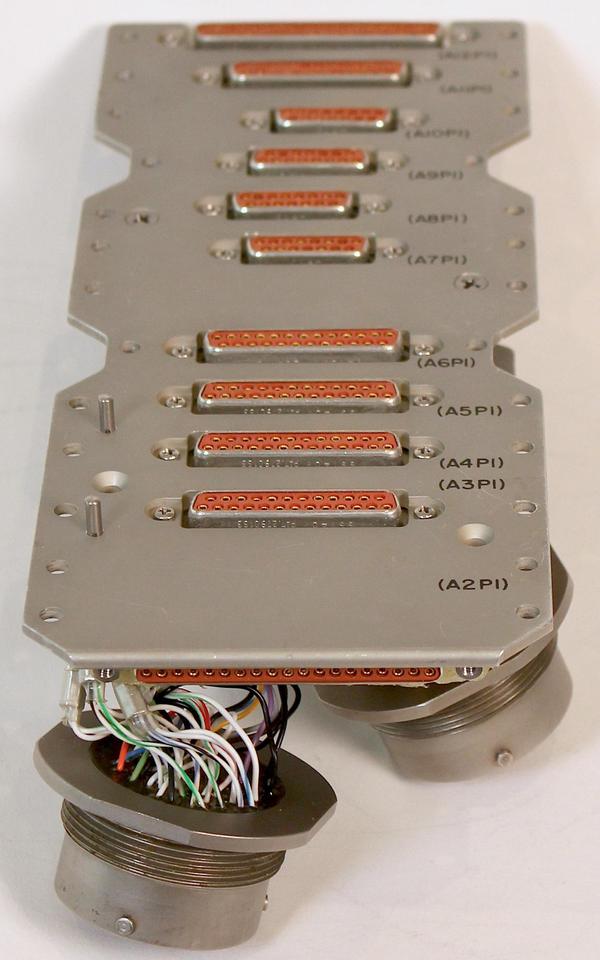
  5. The backplane is a sheet of metal with D-Sub connectors for each module. The round connectors are underneath, wired to the backplane by individual wires.

    The premodulation processor's backplane links the modules to the external connectors.

    The premodulation processor's backplane links the modules to the external connectors.

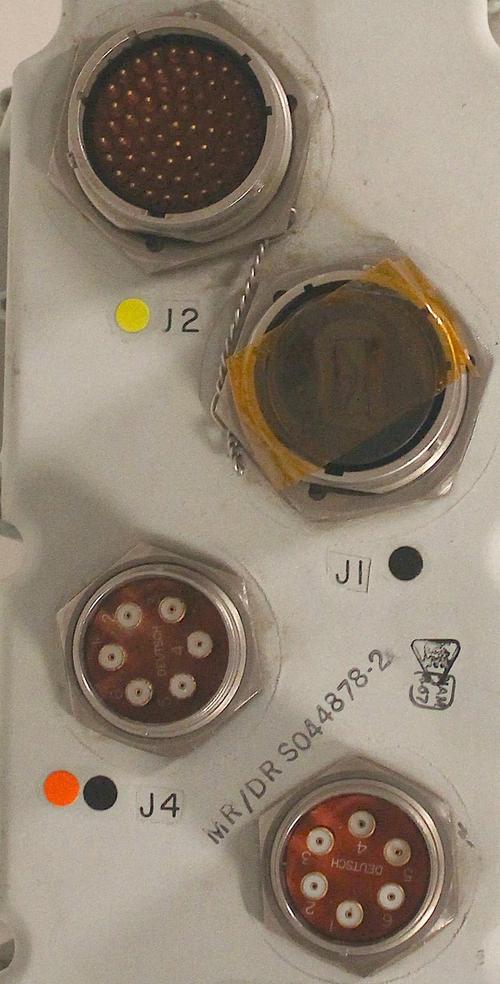
    The four round military-style connectors are shown below. Two connectors have individual pins, while two connectors each have tiny coaxial connections.

    The premodulation processor had four connectors for its numerous audio, RF, and control signals.

    The premodulation processor had four connectors for its numerous audio, RF, and control signals.


  6. We've examined several different Apollo electronics boxes and surprisingly they use completely different manufacturing techniques, even for boxes built by the same manufacturer. Techniques we've seen include printed-circuit boards, surface-mount components, cordwood modules, "dead-bug" components on a ground plane, point-to-point components, and encapsulated hybrid modules. I expected that there would be a standard manufacturing technique (like PCBs are standard now), but everything is different. 

  7. The story of "Set SCE to Aux" is a well-known Apollo incident where disaster was averted. In brief, Apollo 12 was struck twice by lightning just seconds after launch. Inside the spacecraft, so many warning lights lit up that astronaut Conrad thought "the whole board looks like a Christmas tree". On the ground, consoles started displaying nonsense telemetry. Everyone was mystified until engineer John Aaron recalled seeing similar garbled telemetry during a test. He knew the solution and gave the puzzling command "Try SCE to Auxiliary". This switch was so obscure that astronaut Conrad responded, "What the hell is that?" Fortunately, astronaut Bean flipped the switch, bringing the SCE unit back to operation and restoring telemetry. There were other consequences of the lightning strike, but after the fuel cells were brought back online and the inertial guidance system was realigned, the spacecraft continued uneventfully to the Moon.

    The underlying problem was that the lightning strike caused the spacecraft's fuel cells to go offline. The DC voltage bus was supposed to be at 28 volts, but the loss of the fuel cells caused the voltage to sag to about 18 volts. Within milliseconds, the voltage climbed to 24 volts under battery power, still low. The low voltage caused the primary power supply of the SCE (signal conditioning equipment) to shut down. Since the SCE's role was preparing dozens of analog sensor voltages for telemetry, this caused the telemetry values to Mission Control to be garbled. Flipping the SCE switch to Aux caused the SCE to use its auxiliary power supply, restoring the SCE to operation.

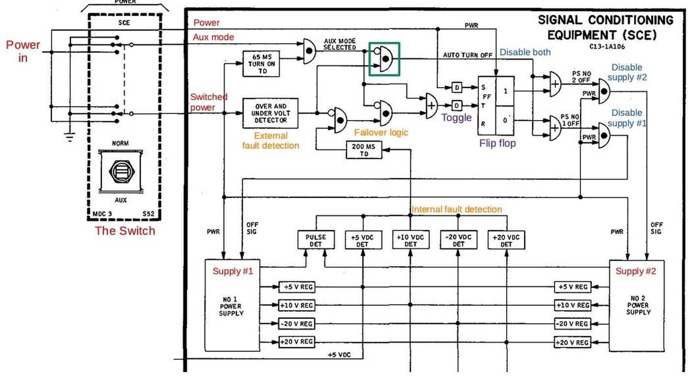
    The published descriptions of this incident are vague on exactly why the auxiliary power supply worked when the primary didn't, so I looked at the SCE diagram (below) to fill in a few details. Power enters at the left and passes through the SCE's famous power switch, which has three positions: NORM, OFF, and AUX. Inside the SCE, there are two power supplies (red) for redundancy, along with some control circuitry at the top. One of the two power supplies is active at a time, unless both power supplies are deactivated for an overvoltage or undervoltage condition.

    Diagram of the SCE power supply and the switch. From Command/Service Module Systems Handbook p118.

    Diagram of the SCE power supply and the switch. From Command/Service Module Systems Handbook p118.

    The SCE has a flip flop (purple) that selects a power supply by disabling (blue) the unused one. When you switch SCE to AUX, one action is that it toggles the flip flop, switching from supply #1 to #2, or #2 to #1. But I don't think that was important for Apollo 12. AUX mode also blocks the undervoltage signal via an AND gate (green). That is, if the input voltage was still too low, both power supplies would be shut down in NORM mode but either one could function in AUX mode. This, I think, is why "SCE to AUX" powered up the SCE.

    Another interesting feature is the automatic failover (orange). In NORM mode, the SCE will automatically switch power supplies if an internal voltage is bad for 200 ms. However, the failover logic is blocked by the undervoltage detector, so it would not have taken place in Apollo 12. But otherwise, if one of the power supplies failed, the SCE would transparently switch to the other one.

    Curiously, the official NASA report Analysis of Apollo 12 Lightning Incident barely has two sentences on the SCE in its 94 pages. Although the SCE gets all the public attention in this incident, it seems like NASA didn't really care about it since the telemetry wasn't critical to the mission. NASA was much more interested in other effects of the lightning strike: the fuel cell shutdown, the effects on the computer and guidance systems, 9 failed sensors, and potential effects on the pyrotechnics. For more on the Apollo 12 incident, see the transcript, the detailed Scott Manley video, and an Apollo Flight Journal post.

    Note that the SCE's power supply logic is different from other units. Most units (such as the transponder, TWT amplifier, and premodulation processor) have primary and secondary power supplies, with a switch to explicitly select one or the other. However, in the SCE, the Aux switch toggles between power supplies, rather than selecting a specific auxiliary power supply. 

  8. Astronauts used multiple switches on the control console to control the premodulation processor. These switches were grouped in the lower-right corner of the console with other communications switches. The diagram below shows the relevant switches, highlighted in yellow.

    The Command Module console contains switches to control the premodulation processor. These switches are highlighted in yellow.
Diagram based on from Command/Service Module Systems Handbook p208.

    The Command Module console contains switches to control the premodulation processor. These switches are highlighted in yellow. Diagram based on from Command/Service Module Systems Handbook p208.

  9. For detailed information on the voice communication system, see Apollo Experience Report - Voice Communications Techniques and Performances. It discusses the performance requirements for the Apollo communications system and how the system was designed to achieve the intelligibility requirements. 

  10. The idea of backup voice was to provide a voice channel for emergencies that used less power, at the cost of garbling up to 30% of the words. After the explosion, Apollo 13 used the backup voice system so they could turn off the Lunar Module's power amplifier and conserve electrical power. (See Apollo 13 Mission Operations Report pages N-2 and N-7, as well as the transcript.) Backup voice was also used at times during Apollo 16 due to a failure of the Lunar Module's steerable S-band antenna; see Apollo 16 Mission Report page 7-3, which calls this mode "down voice backup". (I should point out that these backup voice incidents involved the Lunar Module, not the Command Module's premodulation processor.)