Reverse-engineering a mysterious Univac computer board

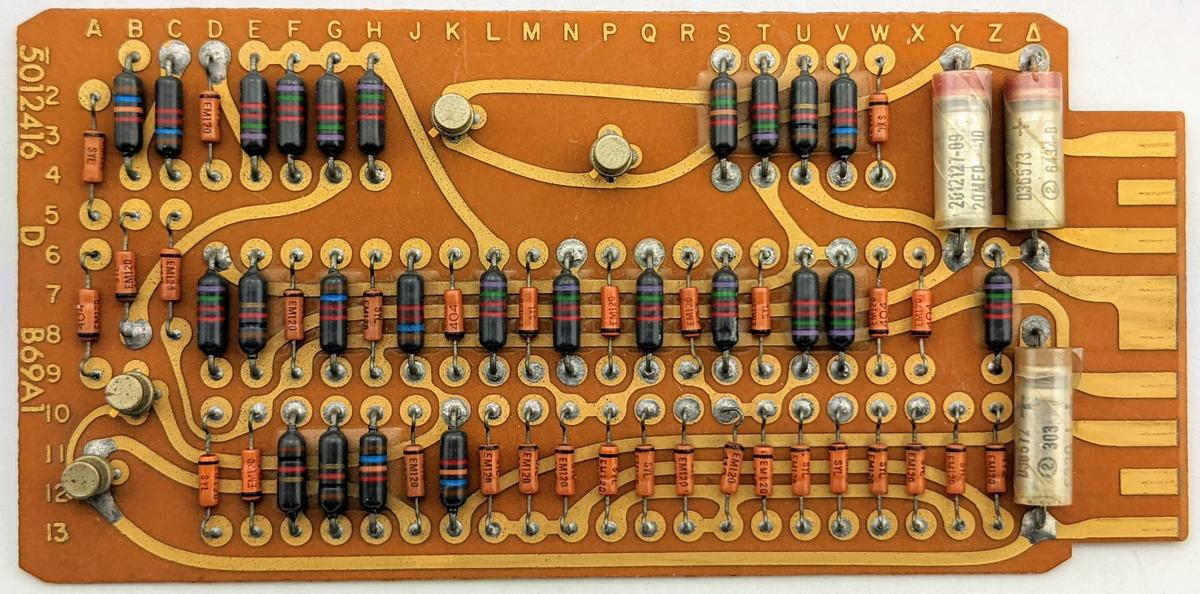
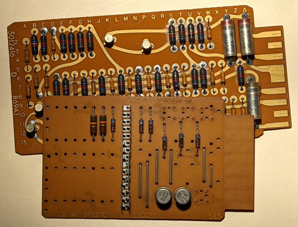
The IBM 1401 team at the Computer History Museum accumulates a lot of mystery components from donations and other sources. While going through a box, we came across the unusual circuit board below. At first, it looked like an IBM SMS (Standard Modular System) card, the building block of IBM's computers of the late 1950s and early 1960s.1 However, this board is larger, has double-sided wiring, the connector is different, and the labeling is different.2

The circuit board is about 15cm×7.3cm.

The circuit board is about 15cm×7.3cm.

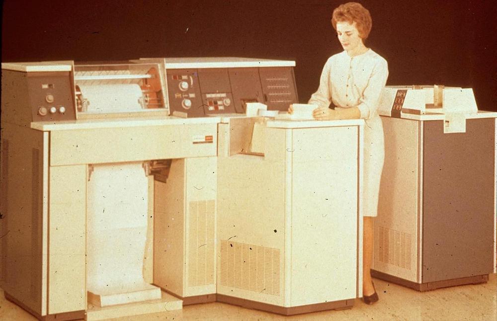
I asked around about the board and Robert Garner identified it as from the Univac 1004, a plugboard-controlled data processing system from 1963.4 The Univac 1004 was marketed as a "Card Processor" rather than a computer,3 designed for business applications that read punch cards and producing output, but still required calculation and logical decisions. Typical applications were payroll, inventory, billing, or accounting.

Photo of the Univac 1004. From bitsavers.

Photo of the Univac 1004. From bitsavers.

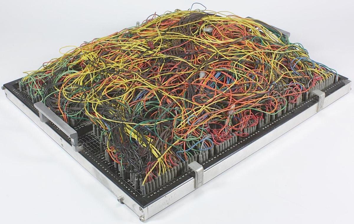
The most unusual feature of the Univac 1004 was that it was programmed by a plugboard (below) instead of a stored program. The system was programmed by plugging patch cords into a plugboard to indicate the desired action for each of the 31 program steps. While earlier electromechanical accounting machines used plugboards, they were pretty much obsolete by 1963, so I was a bit surprised to see plugboards still in use.

A plugboard for the Univac 1004. This board was used for payroll consolidation from 1965 to 1972. From Museums Victoria Collections, Copyright Museums Victoria / CC BY 4.0.

A plugboard for the Univac 1004. This board was used for payroll consolidation from 1965 to 1972. From Museums Victoria Collections, Copyright Museums Victoria / CC BY 4.0.

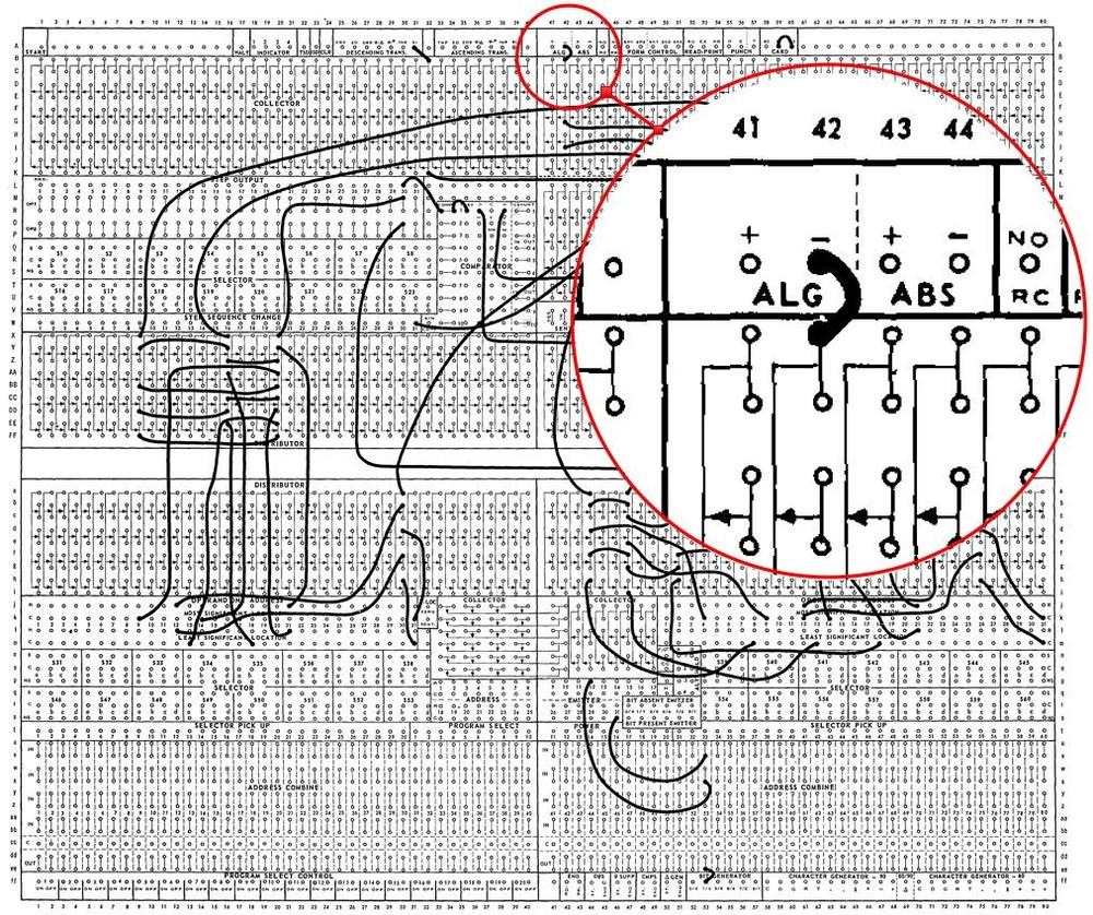
The computer's "program" consisted of 31 steps. The operations for each step were specified by plugging wires into the board. For instance, a data field could be moved from a punch card to memory, a value could be added or subtracted, or a line of output could be configured for the printer.5 The system even supported conditional branches. The diagram below shows the structure of the plugboard. The highlighted wire shows a subtraction operation, activated by the wire in the "algebraic minus" position.

Part of a program in the plugboard.  Click for a larger version. From the Reference Manual.

Part of a program in the plugboard. Click for a larger version. From the Reference Manual.

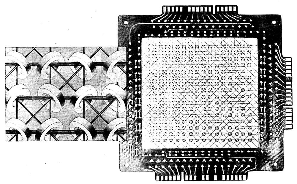
The computer had a small memory of 961 6-bit characters. Like most computers of the era, it used magnetic core memory, storing each bit by magnetizing a tiny ferrite ring. Note that since the computer was programmed through a wiring panel, none of the memory was used for program code.

A plane of magnetic core storage, from the Reference Manual.

A plane of magnetic core storage, from the Reference Manual.

While the Univac 1004 was primitive for its time compared to even a low-end business computer like the IBM 1401, it had a few advantages. First, it rented for $1900 a month, compared to $2500 a month for the IBM 1401 (about $18,000 vs $23,000 a month in current dollars). Second, the Univac computer was compact (by 1960s standards), weighing 2500 pounds. Finally, many customers found plugboard programming easier than programming with code, both because they were more familiar with it and because it is visual and direct.

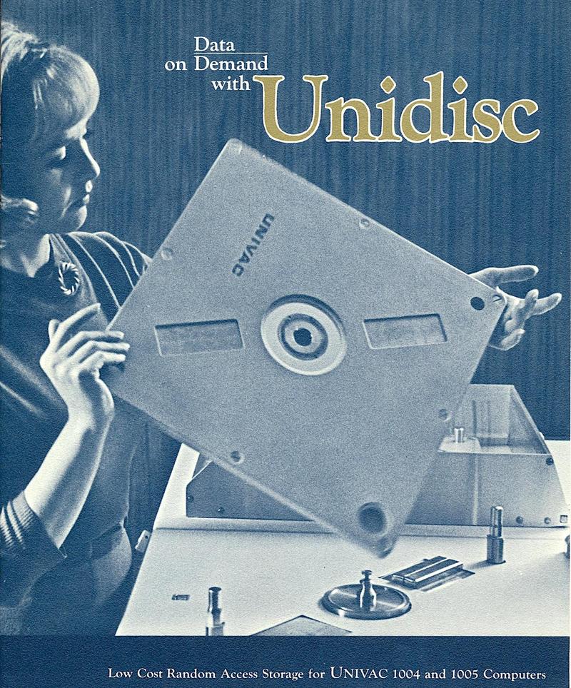
The Univac 1004 could be extended with peripherals such as tape drives, a card punch, or disk storage. The photo below shows the Unidisc cartridge, which held one million characters. Although it looks like an absurdly-large floppy disk, it was a removable hard disk.

The Unidisc cartridge is 15¾ inches square and ⅝-inch thick. (source).

The Unidisc cartridge is 15¾ inches square and ⅝-inch thick. (source).

Reverse-engineering the board

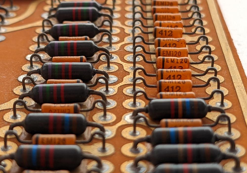
The function of the board wasn't immediately obvious and we had various theories of what it might do. To find out, I reverse-engineered the board by tracing out the circuitry.6 The board has 32 diodes, which seems like a lot, as well as resistors, transistors, and capacitors. The transistors are not silicon transistors, but germanium PNP transistors.

A closeup of the circuit board showing resistors and diodes.

A closeup of the circuit board showing resistors and diodes.

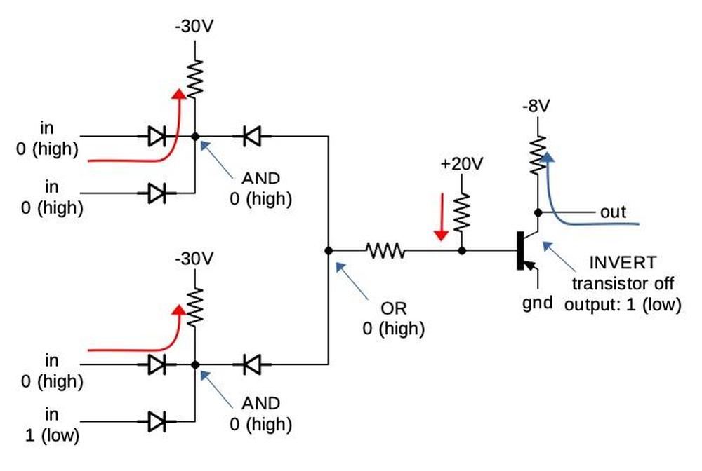
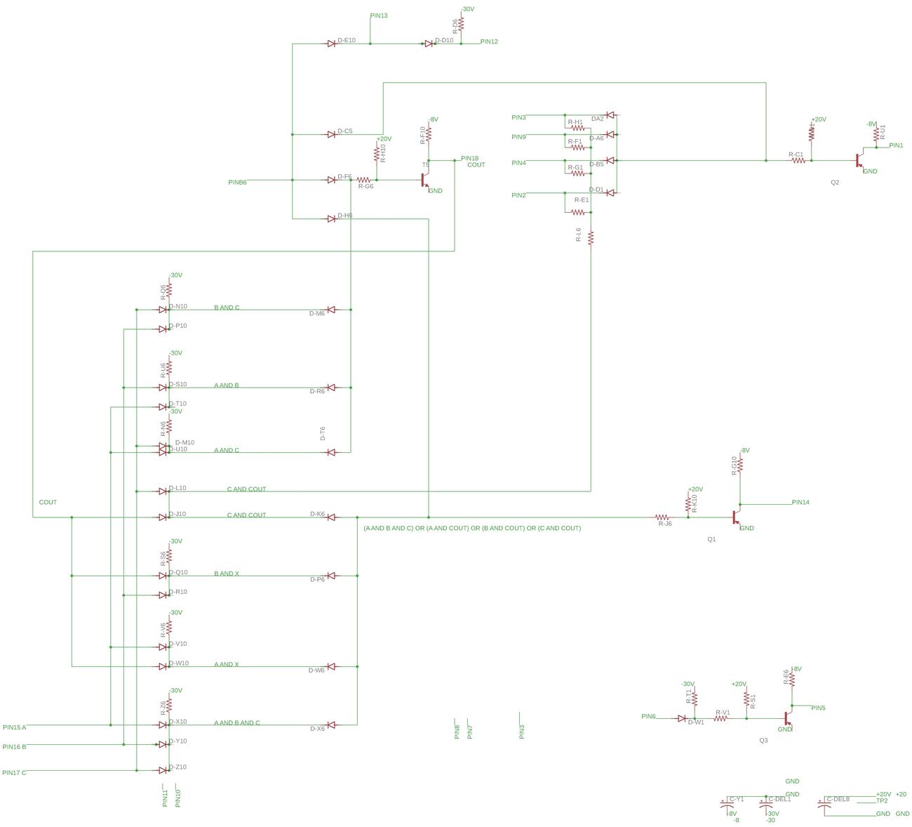
The board turned out to be a logic board implemented with AND-OR-INVERT logic.7 That is, various inputs are ANDed together, the AND results are then ORed together, and finally the result is inverted. The board is implemented with diode-transistor logic. One layer of diodes implements the AND gates and the second layer of diodes implements the OR gates. Finally, a transistor amplifies the result, inverting it in the process. Diode-transistor logic (DTL) performed better than earlier resistor-transistor logic (RTL), but was soon replaced by transistor-transistor logic.

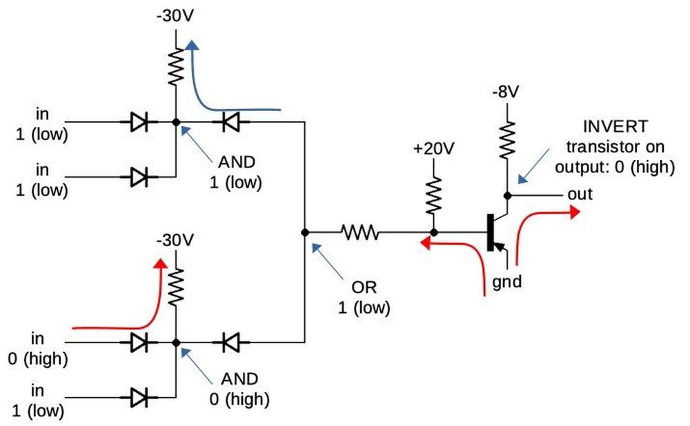
The diagram below explains how the AND-OR-INVERT logic was implemented. This circuit has four inputs: two AND gates that are then ORed together and inverted. (It's a bit confusing because the circuit uses active-low logic, so the voltage levels are all inverted.) If the AND gates all have a 0 (high) input, a diode in the first stage will conduct and pull the AND node high. This blocks the diodes in the second stage (which have the opposite orientation), so the OR node is also high. In the INVERT stage, the +20V resistor will pull the transistor's base high, which turns it off (since it is PNP). Finally, the -8V resistor will pull the output low (i.e. 1), providing the desired AND-OR-INVERT logic.

The AND-OR-INVERT logic producing a 1 output.

The AND-OR-INVERT logic producing a 1 output.

The diagram below shows that if the first AND gate's inputs are 1 (low), the first diodes are blocked, so the -30V resistor pulls the AND node low (1). Now the second-stage diode conducts, pulling the OR node low (1). This allows base current to flow through the PNP transistor, turning it on. This pulls the output high (0). (Note that ground is a high output compared to the low output of -8V.) The gates on the board have more inputs, but use the same principle.

The AND-OR-INVERT logic producing a 0 output.

The AND-OR-INVERT logic producing a 0 output.

After tracing out the board's logic, I recognized that it implemented a full adder.8 That is, it adds two input bits along with a carry-in, producing a sum bit and a carry-out. By connecting four full-adders in series, a 4-bit value can be added, allowing one decimal digit to be added. Thus, the computer probably has four one-bit adder boards similar to this, along with circuitry to convert the output from binary to binary-coded decimal.10

The board has a few additional circuits along with the full adder circuit. It includes an inverter circuit. The board also has 4 inputs that are ANDed, subject to the carry value. Finally, the board also has a disable input that blocks the outputs.9 Without knowing more about the circuitry, I can't determine the role of these circuits.

Conclusion

The mystery circuit board turned out to be from the Univac 1004. Although this computer was produced in the 1960s, its technology occupies an interesting location between the electro-mechanical accounting machines of the 1940s and the electronic business computers of the late 1950s. The Univac computer used transistors and core memory, but it kept the earlier plugboard programming of the accounting machines, rather than moving to stored-program computing (introduced in 1948). Even though the Univac 1004 was technologically backward for 1963, businesses flocked to it, making it the second-most popular computer at the time with 3400 installations.4

This shows that progress isn't as linear as you might expect; "obsolete" technologies can continue to thrive long after the introduction of "superior" alternatives such as stored-program computing. Instead, new systems can still be developed with supposedly-obsolete technologies, depending on the tradeoffs involved.

I announce my latest blog posts on Twitter, so follow me @kenshirriff. I also have an RSS feed.

Notes and references

  1. The Computer History Museum links to a similar board

  2. The photo below compares the Univac board to a smaller IBM SMS board.

    Comparison with an IBM SMS card.

    Comparison with an IBM SMS card.


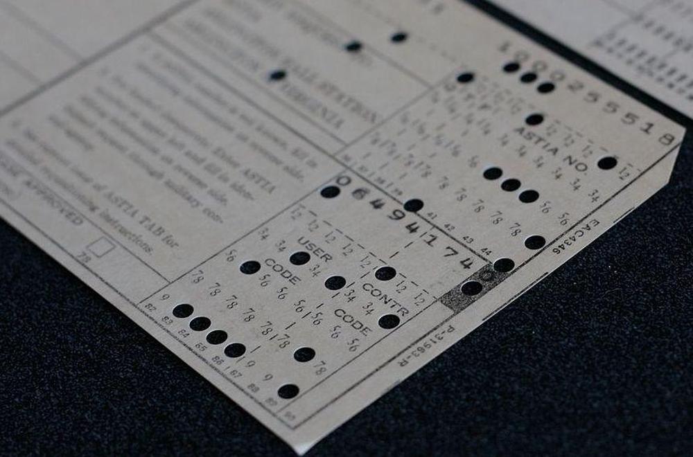
  3. The Univac 1004 computer came in two versions. The "80" read standard IBM 80-column punch cards. The "90" read Univac's 90-column cards (details), which held 90 characters per card instead of 80. The 90-column card was introduced in 1930 by Remington Rand. It had round holes instead of IBM's rectangular holes. The card stored two characters per column by using a denser, binary code. Despite the superior capacity of the 90-column card, IBM's 80-column cards dominated the market. (Even IBM couldn't displace the 80-column card, although they tried with the 96-column card that they introduced in 1969.)

    A 90-column punch card. From Marcin Wichary,  (CC BY 2.0).

    A 90-column punch card. From Marcin Wichary, (CC BY 2.0).


  4. Robert Garner discusses the Univac 1004 briefly in his article on Early Popular Computers. More information is in the 1964 BRL report as well as on Bitsavers. A related board from the Univac 1040/1050 is described here

  5. The plugboard supported conditionals and looping, so I think the system was Turing-complete, although you couldn't do a lot in 31 programming steps. You could implement multiplication or division with a short shift and add (or subtract) loop. 

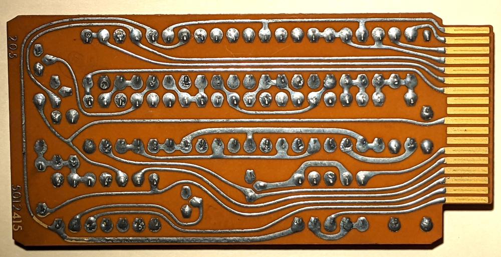
  6. To reverse-engineer the board, I took photos of both sides, flipped the image of the back in GIMP so the two sides were aligned visually, arranged the components on a schematic in EAGLE, and connected the components to match the circuit board. Then I moved the components around until the layout made sense.

    The underside of the circuit board.

    The underside of the circuit board.

    The back of the circuit board is shown above. Note that the edge connectors are completely different on the two sides of the board.


  7. AND-OR-INVERT logic was also used in the IBM System/360 computers, although it was built from hybrid SLT modules instead of discrete components. 

  8. I suspected the board was an adder when I saw that it had three inputs and was combining them symmetrically. The full adder is implemented in AND-OR-INVERT logic as follows. If the two bits are A and B and the carry-in is CIN, then a carry-out (COUT) is generated if at least two input bits are set. This is computed by the AND-OR logic "(A and B) or (A and CIN) or (B and CIN)". The sum bit is set if there is a single 1 input or three 1 inputs. The sum bit was computed by "(A and not COUT) or (B and not COUT) or (CIN and not COUT) or (A and B and CIN)" As a result of the AND-OR-INVERT circuit, the output is inverted. The inverter circuit on the board was probably used to un-invert it. 

  9. The full reverse-engineered schematic is below.

    Reverse-engineered schematic of the board. Click for a larger version.

    Reverse-engineered schematic of the board. Click for a larger version.


  10. The computer uses excess-three encoding for digits, adding 3 to the value before converting to binary. For example, 6 is represented as binary 1001. The advantage of this encoding is that flipping the bits yields the 9's-complement decimal value, simplifying subtraction. For example, flipping the bits of 6 yields binary 0110, which is 3 in excess-3 notation. Excess-3 representation also handles carries correctly; if you add two numbers that sum to 10, the excess-3 values will sum to 16, causing a binary carry. To convert the sum to excess-3, The value 3 must be added (if a carry) or subtracted (if no carry).

    To see how addition works with excess-3, 2 + 4 in excess-3 is binary 0101 + 0111 = 1100. Subtracting 3 yields 1001, which is 6 in excess-3. But 2 + 9 is binary 0101 + 1100 = 10001, generating a carry out of the 4 bit value. Adding 3 yields 0100, which is 1 in excess-3. Considering the carry-out, this is the desired result of 11. 

Inside the Apple-1's shift-register memory

Apple's first product was the Apple-1 computer, introduced exactly 46 years ago, on April 11, 1976. This early microcomputer used an unusual type of storage for its display: shift register memory. Instead of storing data in RAM (random-access memory), it was stored in a 1024-position shift register. You put a bit into the shift register and 1024 clock cycles later, the bit pops out the other end. In the early days of random-access memory chips, shift-register memory was cheaper so many systems used it.1 The downside, of course, is that you had to use bits as they became available, rather than access arbitrary memory locations.2

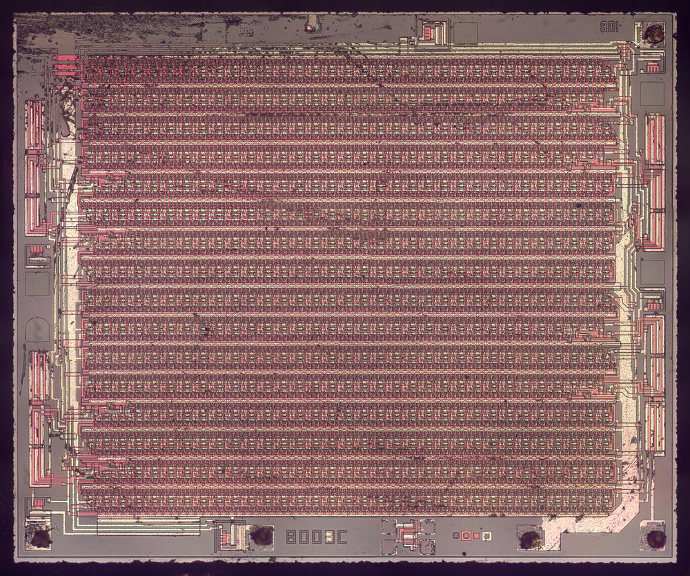
Die of the Signetics 2504 shift register chip. Click this image (or any other) for a larger version.

Die of the Signetics 2504 shift register chip. Click this image (or any other) for a larger version.

The photo above shows the chip under the microscope. The underlying silicon is grayish, with white metal wiring on top. The thickest metal wiring provides power to the chip. The chip also has wiring and transistors constructed from a type of silicon called polysilicon; the polysilicon appears red in the photo. Most of the die is occupied by the shift register, arranged in rows that snake back and forth. The squares around the edge of the die are bond pads, where bond wires connect the die to the chip's external pins.3

The Apple-1's display

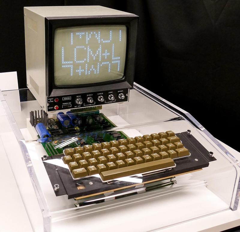
The Apple-1 displayed 24 lines of forty characters on a television monitor. Like most computers at the time, the Apple-1 stored characters rather than pixels to reduce memory requirements. A character-generation ROM converted each character into a 5×7 matrix of pixels as it was displayed. To reduce memory even more, the display didn't store full bytes, but 6-bit characters, supporting upper-case letters, numbers, and some symbols.

The Apple-1 computer was sold as a circuit board. The user had to supply a keyboard, power supply, display, and case. Photo by Cynde Moya, CC BY-SA 4.0.

The Apple-1 computer was sold as a circuit board. The user had to supply a keyboard, power supply, display, and case. Photo by Cynde Moya, CC BY-SA 4.0.

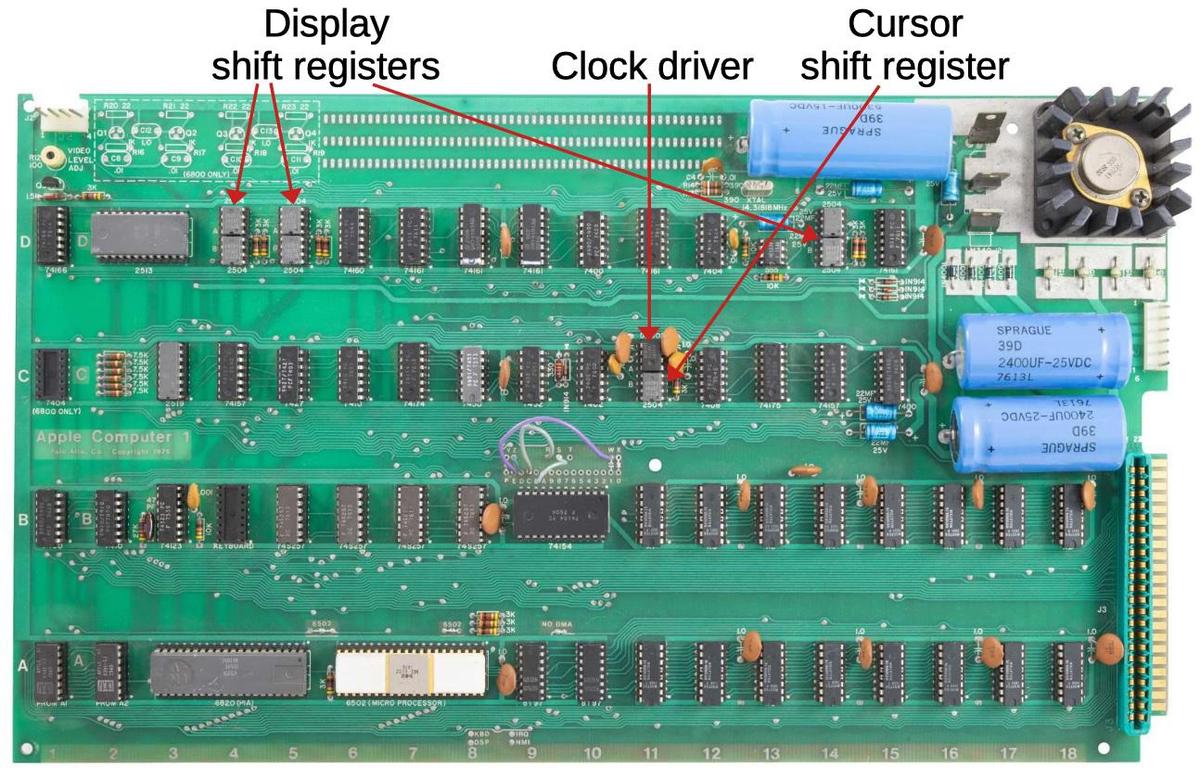
The six-bit display characters were held in six 1024-bit shift registers. A seventh shift register tracked the cursor position.4 The diagram below shows the shift registers and the clock driver on the Apple-1 circuit board. These chips are in 8-pin packages, so two chips fit into the space of a regular TTL chip.5

Apple-1 circuit board, showing the 1024-bit shift register chips and the clock driver chip.
Original image from
Achim Baqué, CC BY-SA 4.0.

Apple-1 circuit board, showing the 1024-bit shift register chips and the clock driver chip. Original image from Achim Baqué, CC BY-SA 4.0.

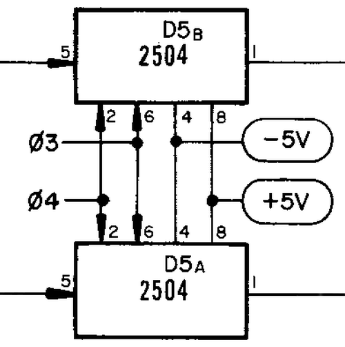
The image below shows how the 2504 shift register chips are represented on the Apple-1 schematic. The chips use just 6 pins. Each chip has a single connection for bits coming in and a connection for the bits coming out. The remaining pins provide the two clock signals and the ±5 volt power supplies. Unlike RAM chips, these chips do not take an address.

Detail of the Apple-1 schematic showing two of the shift register chips.

Detail of the Apple-1 schematic showing two of the shift register chips.

PMOS integrated circuits

This shift register chip was created around 1970, an interesting time in the development of MOS integrated circuits. Early integrated circuits used a type of transistor known as bipolar. However, the metal-oxide-semiconductor (MOS) transistor had the potential to make cheaper, high-density integrated circuits. The first commercial MOS integrated circuit was a 20-bit shift register, created in 1964 by a company called General Microelectronics.

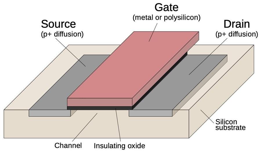
The diagram below shows the structure of a MOS transistor. At the bottom is the silicon, which is doped with impurities to form p-type silicon. The two conductive p-type regions are called the transistor's source and drain. The channel acts as a switch between the source and drain, turned on by voltage in the metal gate above. A thin insulating oxide layer separates the metal gate from the underlying silicon. These three layers—metal, oxide, semiconductor— give the MOS transistor its name. In the late 1960s, chips started to use gates made of polysilicon, a special type of silicon that produced better transistors than metal gates. This is the technology used by the 2504 shift register: the "P-MOS silicon gate process".

Structure of a P-type MOSFET.

Structure of a P-type MOSFET.

By the mid-1970s, however, integrated circuits changed in two more ways. First, P-MOS transistors were replaced by N-MOS transistors, which had better performance. Second, the introduction of ion implantation machines allowed transistor characteristics to be adjusted, with "depletion-mode" transistors8 leading to faster, lower-power circuitry. These changes ushered in the age of popular microprocessors such as the Zilog Z80, MOS Technology 6502, and Intel 8085. These had much better performance than earlier PMOS processors such as the Intel 8008.7 The 6502, of course, was the processor in the Apple-1 (and Apple II).

The shift register

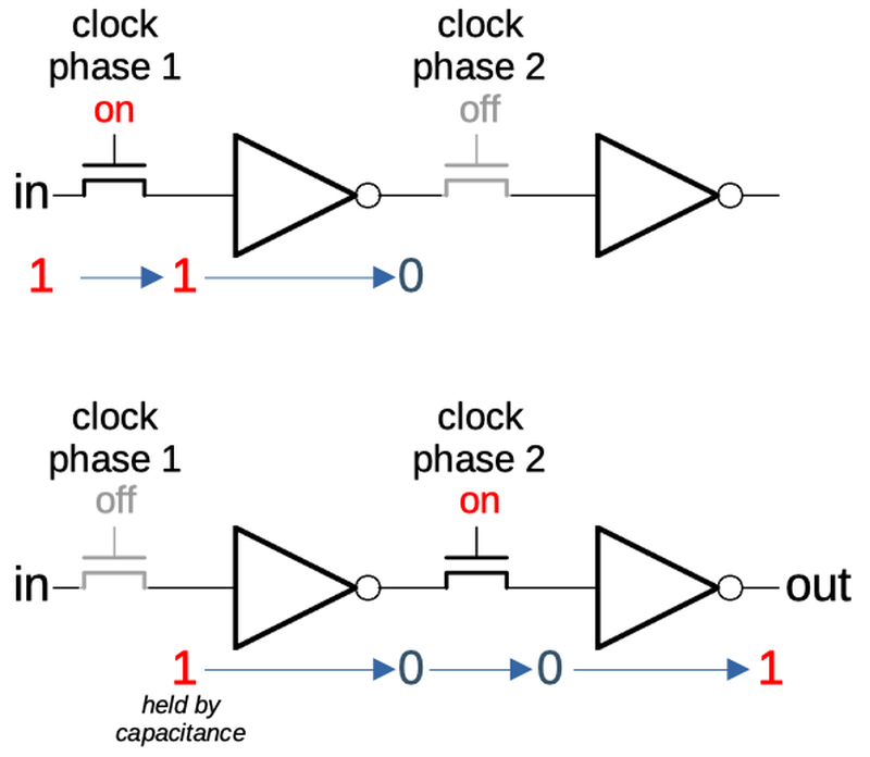
Next, I'll look at the details of how the shift register was constructed. The idea of a shift register is that bits are passed from stage to stage, controlled by clock pulses. With 1024 stages, the shift register can hold 1024 bits. Each shift register stage uses two transistors and two inverters as shown below. During the first clock phase, the first transistor turns on, allowing the input bit to pass through it and the first inverter. During the second clock phase, the second transistor turns on, allowing the inverted value to pass through it and the second inverter, producing the output. Thus, a bit takes two clock phases to move through the shift register stage.

In the first clock phase, the input passes through the first transistor. In the second clock phase, the input is held by the gate capacitance and passes to the output.

In the first clock phase, the input passes through the first transistor. In the second clock phase, the input is held by the gate capacitance and passes to the output.

This circuit is a dynamic shift register, which works due to the circuit's capacitance. When the first transistor turns off, the value remains at the input to the first inverter, held by the capacitance of the circuit. (And likewise for the second transistor.) Because the gate of a MOSFET uses almost no current, the bit value will remain for a couple of milliseconds or so before it drains away. (This is the same principle used by DRAM, holding bits through capacitance.) As long as the clock keeps going, the bit gets refreshed by each stage.

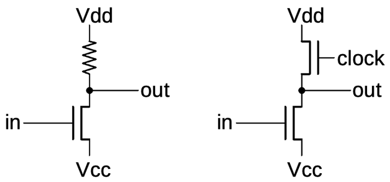
Each inverter is implemented using two MOS transistors. The concept is shown on the left, below. A high input turns on the transistor, which pulls the output low. A low input turns off the transistor allowing the pull-up resistor to pull the output high. Thus, the circuit inverts its input.

Conceptually, the inverter uses the circuit on the left. The implementation uses the circuit on the right.

Conceptually, the inverter uses the circuit on the left. The implementation uses the circuit on the right.

The circuit is actually implemented with a transistor in place of the resistor, as shown on the right, because transistors are more compact than resistors. A high input to the upper transistor turns it on, causing the pull-up current to flow. In a standard inverter, the transistor would be connected to be always on.9 However, the output of the inverter is only used during one clock phase. To reduce power consumption, the transistor is wired to the clock so it only acts as a pull-up when needed.

A shift-register stage on the die

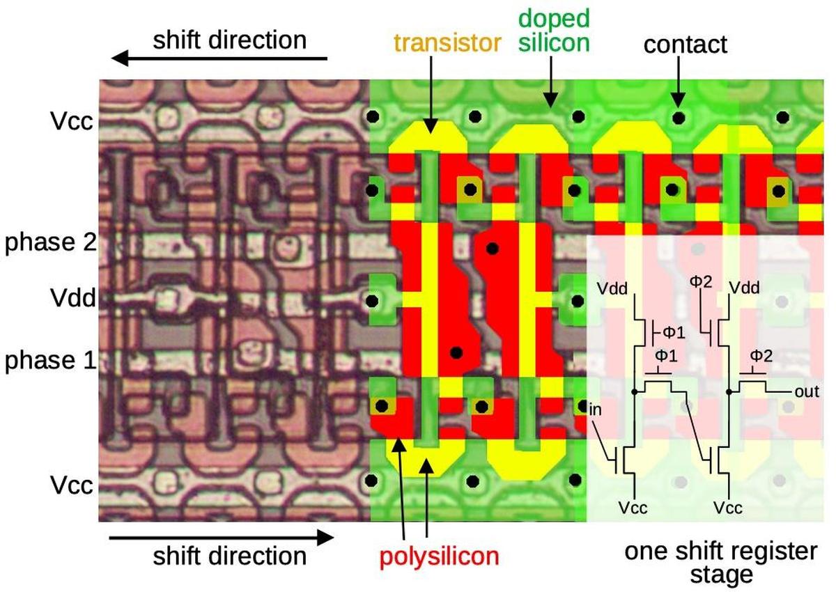
The diagram below shows how shift-register stages are physically constructed on the die. The first part of the image shows how the circuitry appears under the microscope, a complicated jumble of silicon, polysilicon, and metal circuitry. In the middle, I've highlighted the doped silicon in green and the polysilicon in red. A transistor gate (yellow) is formed where polysilicon crosses silicon, with the source and drain on either side. (The horizontal metal wiring should be clear without highlighting.) Note the complex, optimized shapes of the polysilicon and the transistors. Finally, a black dot indicates a contact that connects two layers. In the bottom half of the image, bits are shifted to the right, while in the top half, bits are shifted to the left.

One stage of the shift register.

One stage of the shift register.

In the lower right, one stage of the shift register is represented by a schematic on top of the underlying circuitry. The stage is implemented with six transistors as described earlier. Note that the pull-up transistors to Vdd are long and skinny, reducing their current. The inverter transistors to Vcc, on the other hand, are wide, so they provide a lot of current. The circuitry in the top half of the image is the same, but rotated 180°. Note that the two rows of shift registers share the clock phase lines and Vdd, making the layout more efficient.6

Topology of the chip

You might expect the chip to consist of 1024 shift-register stages arranged into a chain. However, the chip had an unusual topology that allowed it to operate at double speed: one bit per clock phase instead of one bit per complete clock cycle. It accomplished this with a simple trick: it was really two 512-bit shift registers operating in parallel. The first operated on clock phase 1, phase 2, phase 1, ..., while the second was the opposite: phase 2, phase 1, phase 2, ... The result was that one half would produce bits in phase 1, while the other would produce bits in phase 2. The output circuit merged these together into a single output stream. From the outside, it looked like a 1024-bit shift register that operated twice as fast.

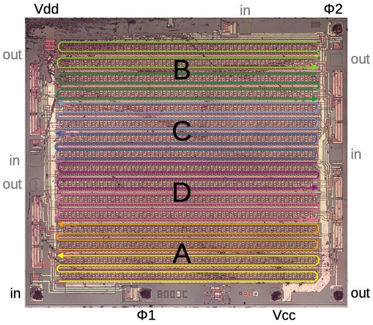
Another complication is that Signetics produced three 1024-bit shift register chips from the same silicon layout: the 2502 (organized as four 256-bit shift registers), the 2503 (512×2), and the Apple-1's 2504 (1024×1). The different chips were created by changing the metal wiring of the chip during manufacturing, which was much easier than building completely different chips. To support this, the shift register was broken into eight 128-bit segments, shown below. In the 1024×1 chip, two chains of four 128-bit segments ran in parallel (on opposite clock phases) to produce a 1024-bit shift register. The first chain used the light-colored segments A, B, C, D, while the second chain used the dark-colored segments. The segments are connected by the metal wiring along the side of the die. The chip's pads around the edges are labeled; the grayed-out ones are not used in this chip. The large block of circuitry above the output pin combines the two chains into one output.

The chip consists of 8 shift-register chains, each 128 bits long. They are connected in different ways to form different shift register chips.

The chip consists of 8 shift-register chains, each 128 bits long. They are connected in different ways to form different shift register chips.

The other variants of the chip wire the shift-register segments differently and use additional input and output pins. The 512×2 2503 chip used four chains of 256 bits along with two input and output circuits. The 2502B chip used all eight 128-bit chains in parallel to form a 256×4 shift register, with four input and output circuits.10

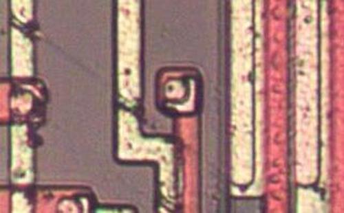
The image below shows one of the unconnected outputs: the red polysilicon wire isn't connected at one end. With a small change to the metal layer, the metal wiring between two segments can be broken and the segment wired to this output instead. The other changes between chip versions are similar.

The polysilicon wire in the middle is disconnected.

The polysilicon wire in the middle is disconnected.

The clock driver

I'll wrap up with a brief mention of the clock driver chip that drives the shift registers. Shift-register memory chips required clock pulses with high current and unusual voltages due to the PMOS circuitry: from +5 volts to -11 volts. These pulses were provided by a special chip, the DS0025 Two-Phase MOS Clock Driver. The die photo below shows this chip. The die is dominated by four power transistors that produced 1.5 amp pulses. I wrote a blog post about the clock driver chip if you want more details.

Die photo of the DS0025 clock driver chip.

Die photo of the DS0025 clock driver chip.

Conclusion

The Apple-1 is now a collector's item, with boards selling for hundreds of thousands of dollars. However, when it was introduced in 1976, it wasn't a particularly important computer, with about 200 sold at the price of $666.66. The Apple II, which came out a year later in 1977, was a much more influential computer, selling millions to become one of the archetypical home computers of that era. The Apple II used RAM chips for all its storage, illustrating that shift-register memory had rapidly become obsolete.

The shift-register chip illustrates the amazing decline in memory prices, as reflected by Moore's Law. This 1-kilobit shift register cost about $60 (in current dollars), while a 16-gigabit DRAM chip now costs about $6. Thus, memory is about 160 million times cheaper now, an amazing drop.

I announce my latest blog posts on Twitter, so follow me @kenshirriff. I also have an RSS feed. Thanks to @TubeTimeUS for supplying the chip. I've written about the Intel 1405 shift register memory if you want to know more about this type of storage.

Notes and references

  1. The first reference to the Signetics 2504 that I could find was in 1970, when each chip cost $11.05 in quantities of 100 (about $60 in current dollars). Looking in an old Byte magazine from 1976, a 1-kilobit shift register chip cost $9 ($34 in current dollars), while a 4-kilobit DRAM chip cost $20 ($75 in current dollars). Thus, it appears that even by the time the Apple-1 was released, DRAMs had become cheaper than shift registers.

    The Apple-1 used 4-kilobit RAM for data and program storage. It's possible, though, to build a computer that uses shift-register storage for its main memory. The Datapoint 2200 is one example. If memory is accessed sequentially, shift-register storage is efficient since the bits are provided sequentially. However, if you access memory out of sequence, the processor has to wait while the memory cycles around, until the desired bits become available. In a way, shift-register memory is a throwback to very early computers such as EDSAC (1949), which used mercury delay lines for main storage. 

  2. The behavior of shift-register memory was a good match for video circuitry, since characters are displayed on the screen in a fixed, repeating order (left to right and top to bottom). The IBM 2260 video display terminal (1965) used a technique similar to shift registers: it stored data in a sonic delay line, sending torsional pulses through a 50-foot nickel wire. But unlike the Apple-1, this delay line stored pixels, not characters. For more about this system, see my blog post

  3. The die was encased in an epoxy package. To expose the die, Eric (@TubeTimeUS) tediously sanded through the plastic package until the die was visible. There are a few scratches on the die from this process, especially in the upper left. 

  4. The display circuitry has some additional complexity. Characters can't be taken directly from the display shift register: since each character is made up of eight scan lines; a line of character must be processed eight times. To handle this, a second shift register (six 40-bit registers) buffers a line of characters and feeds each character into a display ROM. Another 1024-bit shift register keeps track of the cursor position. For more details, see stackexchange

  5. The Apple-1 display has a lot of similarity with the popular TV Typewriter, a hobbyist video terminal kit from 1973. The TV Typewriter used shift-register memory for its 32×16 display, but had a complex 5-board design. Wozniak's design for the Apple-1 was much simpler. 

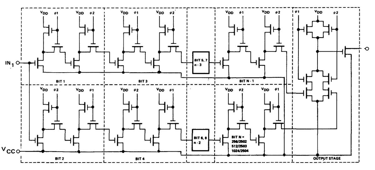
  6. The schematic of the chip is shown below. Notice the upper and lower shift registers, which run on opposite clock phases. Apart from the 6-transistor shift-register stages, the only circuitry is the output stage that merges the two results and drives the output pin.

    Schematic of the chip. Click for a larger image. From the 1972 databook.

    Schematic of the chip. Click for a larger image. From the 1972 databook.


  7. Another major improvement in integrated circuits was the introduction of CMOS, which used NMOS and PMOS transistors together, with much lower power consumption. By the 1980s, processors such as the Intel 80386 (1985) and Motorola 68030 (1987) used CMOS. CMOS is still used in modern integrated circuits. 

  8. In the mid-1970s, ion implantation technology allowed the creation of depletion-mode transistors. These transistors could be used as pull-up elements, called depletion loads. Since depletion-load transistors could operate faster and with less current, they rapidly became a standard part of MOS integrated circuits, until replaced by CMOS in the 1980s. The Zilog Z80 and Intel 2102 SRAM were two early chips that used depletion loads. 

  9. You might think that the inverter circuit will result in a short circuit between Vdd and Vcc when both the input and the clock are high. However, the pull-up transistor is designed to produce a weak current, so the other transistor can still pull the output low. This current results in relatively high power consumption for PMOS or NMOS circuitry, a problem that is fixed by CMOS. 

  10. The 256×4 2502B chip required a 16-pin package, rather than the 8-pin package of other chips, due to the additional input and output pins. 

Inside the Apple-1's unusual MOS clock driver chip

Apple's first product was the Apple-1 computer, introduced in 1976. This early microcomputer used an unusual type of storage for its display: shift register memory. Instead of storing data in RAM (random-access memory), it was stored in a 1024-position shift register. You put a bit into the shift register and 1024 clock cycles later, the bit pops out the other end. Since a shift-register memory didn't require addressing circuitry, it could be manufactured more cheaply than a random-access memory chip.1 The downside, of course, is that you had to use bits as they became available, rather than access arbitrary memory locations. The behavior of shift-register memory was a good match for video circuitry, though, since characters are displayed on the screen in a fixed, repeating order (left to right and top to bottom).2


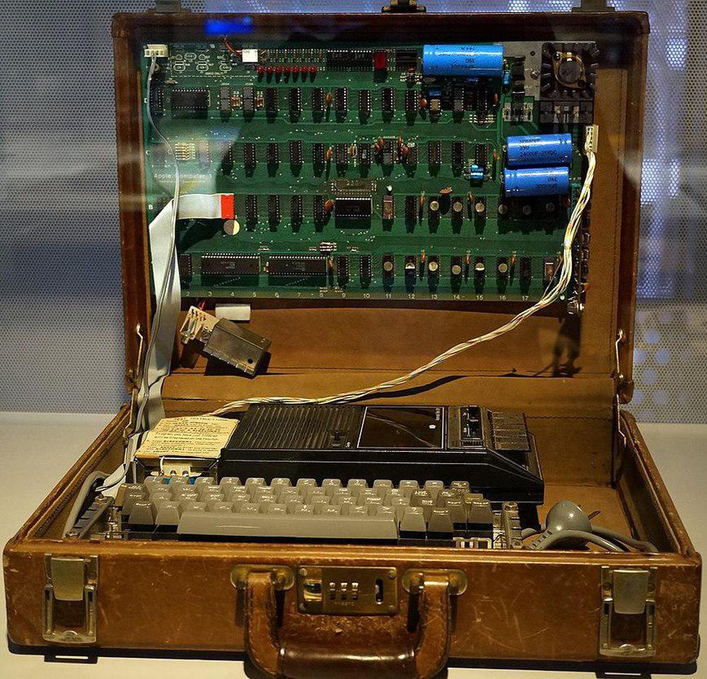
The Apple-1 was sold as a bare board, so users needed to make a case for it, or mount it in a briefcase as shown here.
Note the cassette drive used for mass storage.
Photo cropped from Binarysequence, CC BY-SA 4.0.

The Apple-1 was sold as a bare board, so users needed to make a case for it, or mount it in a briefcase as shown here. Note the cassette drive used for mass storage. Photo cropped from Binarysequence, CC BY-SA 4.0.

Shift-register memory chips required clock pulses with high current and unusual voltages: from +5 volts to -11 volts. These pulses were provided by a special chip, the DS0025 Two-Phase MOS Clock Driver. This chip, introduced in 1969, was the first monolithic (i.e. integrated circuit) clock driver. In this blog post, I look inside the chip and explain how it was implemented.

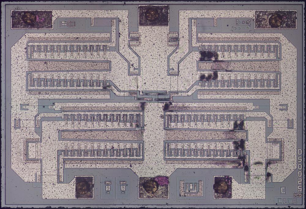
Die of the DS0025 clock driver. Click this image (or any other) for a larger version.

Die of the DS0025 clock driver. Click this image (or any other) for a larger version.

The photo above shows the silicon die under the microscope. This chip is very simple, containing four large NPN transistors, four diodes, and four resistors. The silicon appears blue-gray in this image, while the metal layer on top appears speckled white. Around the outside of the die, are six dark rectangles, the pads where golden bond wires connected the die to the chip's external pins.

The die was encased in an epoxy package. To expose the die, Eric (@TubeTimeUS) tediously sanded through the plastic package until the die was visible. Some bits of epoxy remained, caught in the bond wires, so I cleaned up the die with a few drops of boiling sulfuric acid.

The Apple-1's display

The Apple-1 displayed 24 lines of forty characters on a television monitor. Like most computers at the time, the Apple-1 stored characters rather than pixels to reduce memory requirements. A character-generation ROM converted each character into a 5×7 matrix of pixels as it was displayed. To reduce memory even more, the display didn't store full bytes, but 6-bit characters, supporting upper-case letters, numbers, and some symbols.

The six-bit display characters were held in six 1024-bit shift registers. A seventh shift register tracked the cursor position.3 The diagram below shows the shift registers and the clock driver on the Apple-1 circuit board. These chips are in 8-pin packages, so two chips fit into the space of a regular TTL chip.

Apple-1 circuit board, showing the 1024-bit shift register chips and the clock driver chip.
Original image from
Achim Baqué, CC BY-SA 4.0.

Apple-1 circuit board, showing the 1024-bit shift register chips and the clock driver chip. Original image from Achim Baqué, CC BY-SA 4.0.

Transistors

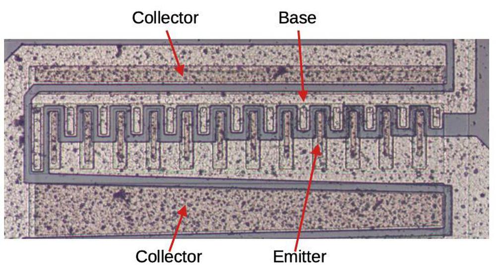
Next, I'll discuss the components of the chip. Because the chip generates high-current pulses, it uses large NPN transistors, with a different construction from most integrated circuit transistors. Each transistor consists of 24 emitters, paralleled in two groups. (You can consider it one large transistor, 2 transistors, or 24 small transistors.) The transistor is structured vertically with the collector (made of N-doped silicon) underneath, a thin P-type base in between, and the N-type emitters embedded in the top, forming the N-P-N layers of the transistor. The doped silicon regions are faintly visible with black lines around their boundaries.

Half of a transistor, with 12 emitters.

Half of a transistor, with 12 emitters.

In the photo above, you can see the metal wiring for the transistor's collector, base, and emitter. The collector wiring is on the outside, with base wiring in between. The collector and emitter wiring is tapered: at one end, the wiring needs to support the full current load, while at the other end it only handles 1/12 of the current. The tapered approach saves space, since it is thicker only where it needs to be thick.

Resistors

The resistors are formed from silicon doped to have higher resistance. The doped silicon rectangle is faintly visible in the die photo. At each end of the resistor, a contact connects the silicon to the metal layer on top. The 1000Ω resistor on the left is longer than the 250Ω resistor on the right, giving it more resistance.

Two resistors as they appear on the die.

Two resistors as they appear on the die.

"Tunnels"

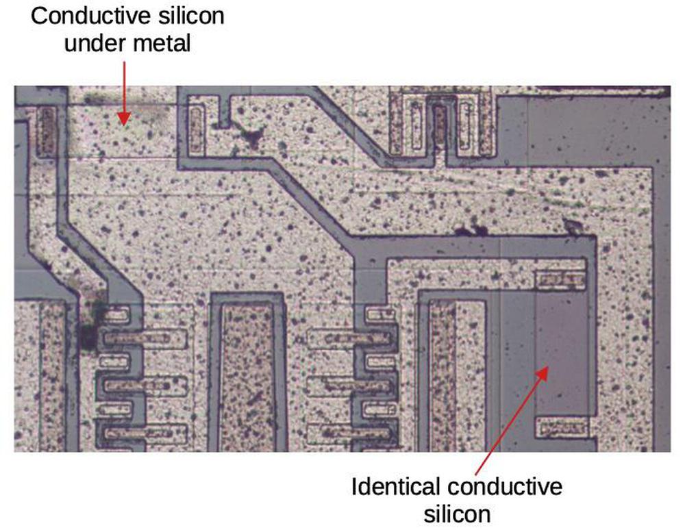
The chip has a single layer of metal wiring, which poses a problem if two signals need to cross. The solution is to put one signal in the silicon layer so it can pass under the metal layer. In essence, a low-valued resistor is used to pass under the metal layer. The image below shows how a tunnel appears on the die.

The conductive silicon strip at the top connects the metal regions on either side. The conductive strip at the bottom doesn't fulfill a wiring need, but ensures that both paths encounter the same resistance.

The conductive silicon strip at the top connects the metal regions on either side. The conductive strip at the bottom doesn't fulfill a wiring need, but ensures that both paths encounter the same resistance.

One problem is that the silicon has relatively high resistance compared to metal, so the tunnel adds resistance. The chip is carefully designed so both "sub-transistors" encounter the same resistance, to avoid one transistor turning on before the other. You can see that the input path in the upper left has a tunnel to pass under the metal wiring, while the path in the lower right has a tunnel of identical dimensions that doesn't go under any metal. While the second tunnel appears pointless, it assures that both paths have the same resistance.

The chip's circuit

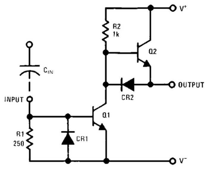
The shift register requires a two-phase clock, that is two clock signals in alternation that step the bits through the circuit. To support this, the clock driver chip has two identical driver circuits. The schematic below shows one of the circuits. When the input goes high, it turns on transistor Q1, pulling its collector low. This pulls the output low through diode CR2. When the input drops, Q1 turns off. This lets R2 provide a current to the base of Q2, turning it on, and pulling the output high. Thus, the circuit is essentially an inverter, but one that can provide up to 1.5 amps of output.4

Schematic of the DS0025, from the application note.

Schematic of the DS0025, from the application note.

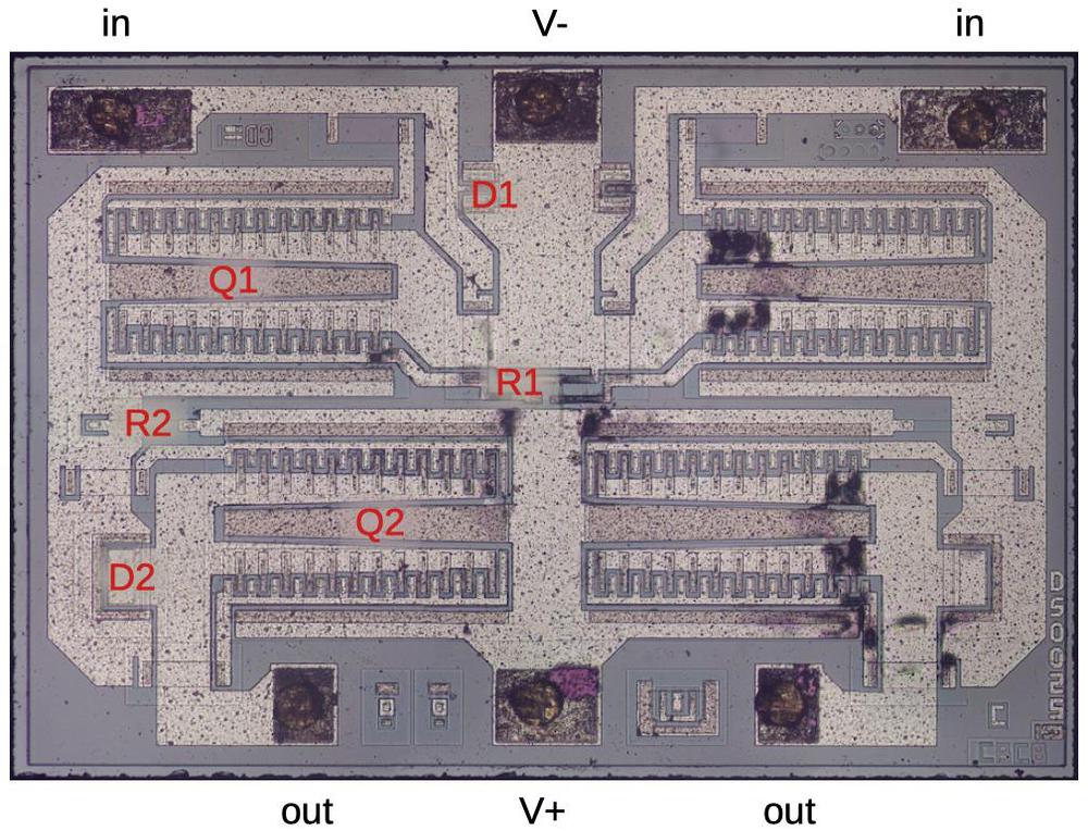
The image below shows the various components of the schematic as they appear on the die. Most of the chip is occupied by the large power transistors. Although the chip is mounted in an 8-pin package, only six pins are used; the corresponding pads are labeled below. The chip consists of two identical mirror-image drivers; one is labeled. There are a few blackened regions in the transistors; we suspect this is where the chip failed.

Die with the components labeled.

Die with the components labeled. Note: diodes are labeled CR (crystal rectifier) in the schematic but D here.

Conclusion

This chip provides an interesting view of computer technology in the 1970s. The Apple-1 used shift-register memory, a technology that rapidly became obsolete as RAM prices dropped. Shift-register memory required a specialized clock driver integrated circuit, a chip that contained just four large transistors. With billions of transistors in modern integrated circuits, it's hard to imagine that it was once worthwhile to build a chip that was this simple. The Apple II, introduced just a year later in 1977, used RAM chips for all its storage, making shift-register memory a thing of the past.

I announce my latest blog posts on Twitter, so follow me @kenshirriff. I also have an RSS feed. Thanks to @TubeTimeUS for supplying the chip. I've written about the Intel 1405 shift register memory if you want to know more about this type of storage.

Notes and references

  1. Looking in an old Byte magazine from 1976, a 1-kilobit shift register chip cost $9 ($34 in current dollars), while a 4-kilobit DRAM chip cost $20 ($75 in current dollars). Thus, it appears that even by the time the Apple-1 was released, DRAMs had become cheaper than shift registers. (This also illustrates the amazing drop in memory prices since the 1970s, as described by Moore's Law.)

    The Apple-1 used 4-kilobit RAM for data and program storage. It's possible, though, to build a computer that uses shift-register storage for its main memory. The Datapoint 2200 is one example. If memory is accessed sequentially, shift-register storage is efficient since the bits are provided sequentially. However, if you access memory out of sequence, the processor has to wait while the memory cycles around, until the desired bits become available. In a way, shift-register memory is a throwback to very early computers such as EDSAC(1949), which used mercury delay lines for main storage. 

  2. The IBM 2260 video display terminal (1965) used a technique similar to shift registers: it stored data in a sonic delay line, sending torsional pulses through a 50-foot nickel wire. But unlike the Apple-1, this delay line stored pixels, not characters. For more about this system, see my blog post

  3. The display circuitry has some additional complexity. Characters can't be taken directly from the display shift register: since each character is made up of eight scan lines; a line of character must be processed eight times. To handle this, a second shift register (six 40-bit registers) buffers a line of characters and feeds each character into a display ROM. Another 1024-bit shift register keeps track of the cursor position. For more details, see this post. The Apple-1 schematic is in the Operation Manual

  4. The large current is required because of the design of the shift-register memory. The clock line snakes through the chip, providing a clock signal to each stage of the shift register. As a result, the clock line has a fairly high capacitance, about 150 picofarads. This clock line must be switched between +5 volts and -11 volts at a 1 megahertz rate. The combination of large capacitance and large voltage swing with the fast rate requires a high current. 

Reverse-engineering the waveform generator in a 1969 breadboard

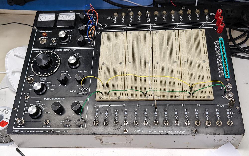
How hard could it be to fix a vintage solderless breadboard that doesn't quite work? The "elite 2 circuit design test system" below combined a solderless breadboard with some supporting circuitry: power supplies, a waveform generator, a pulse generator, switches, and lights. CuriousMarc found one of these breadboards on eBay, but the function generator didn't work, so we set out to repair it.

The E&L Instruments elite 2 solderless breadboard has a variety of supporting circuitry.

The E&L Instruments elite 2 solderless breadboard has a variety of supporting circuitry.

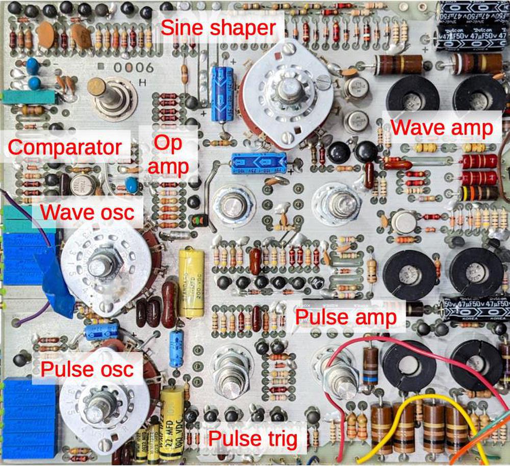
I figured that the waveform and pulse generators would be simple circuits, but they turn out to be implemented with a board crammed full of components, including over 40 transistors. I reverse-engineered the circuitry and found some interesting circuits inside, including op-amps implemented from discrete transistors. This complexity probably explains the shockingly high price of this breadboard: $1300 in 1969 (equivalent to $10,000 in current dollars).1

The circuit board for the function/pulse generator is crammed full of components. The upper part holds the waveform circuitry while the lower part holds the pulse generator.

The circuit board for the function/pulse generator is crammed full of components. The upper part holds the waveform circuitry while the lower part holds the pulse generator.

The waveform generator

The breadboard has a waveform generator that produces triangle, square, and sine waves over a wide frequency range, up to 1 megahertz. These waveforms are generated through a complex circuit that charges and discharges an integrator to produce the triangle wave. A comparator turns the triangle wave into a square wave. Finally, a sine-wave shaping network produces a sine wave from the triangle wave.

Triangle-wave generator

The oscillator's frequency is selected by resistors and capacitors. The faster the capacitor charges through the resistor, the higher the frequency. Thus, increasing the capacitance and resistance slows the oscillation. The frequency range knob turns a vintage wafer rotary switch to select one of seven different resistors and capacitors, allowing frequencies over a wide range from 1 Hertz to 1 megahertz. A potentiometer adjusts the frequency within the range to provide the exact desired frequency.

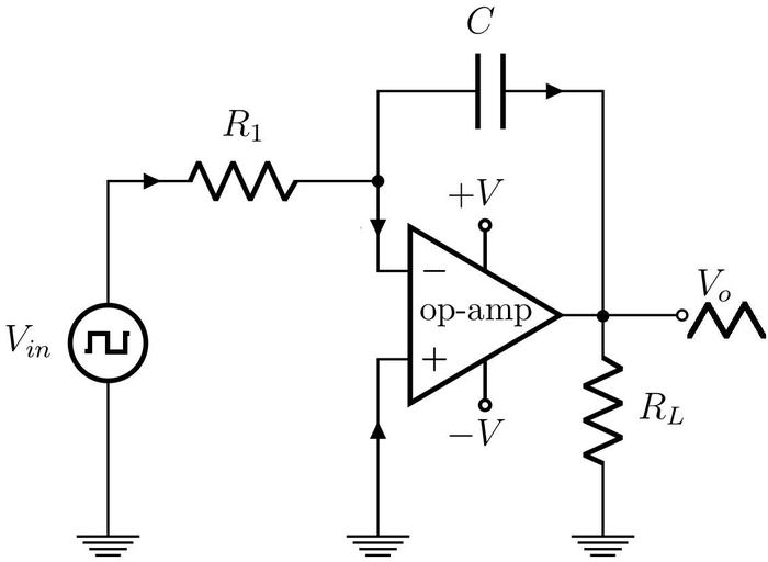
The triangle wave is generated from an op-amp integrator circuit, using the approach below. This circuit uses the capacitor to integrate the input voltage, producing the output voltage. The result is that the square wave input increases or decreases the output linearly, yielding a triangle wave. (The op-amp keeps that right side of R1 at ground, so the current that charges the capacitor is proportional to the input voltage. In contrast, in a simple R-C charging circuit, the capacitor charges exponentially; the charging current drops as the capacitor's voltage increases.)

A simplified op-amp integrator, based on image by Rutujadeshpande, CC BY-SA 3.0.

A simplified op-amp integrator, based on image by Rutujadeshpande, CC BY-SA 3.0.

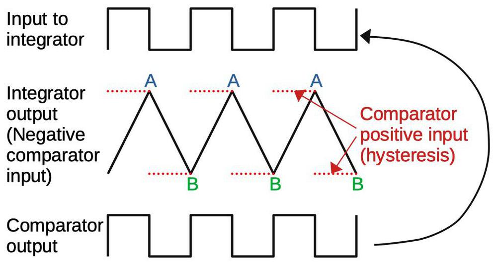
To make an oscillator, the other piece is a comparator to provide the square wave input to the integrator. The comparator reverses direction at the top and bottom of the triangle wave, as shown below. When the input to the integrator is positive, the integrator output climbs linearly. This output is fed into the comparator, along with a limit level (red dots). When the output exceeds the upper limit at "A", the comparator output becomes negative. Since the comparator output is used as the integrator input, the integrator now discharges and the signal drops. When the signal drops below the limit at B, the comparator switches on and the process repeats. A hysteresis circuit changes the comparator level (dotted red line) at A and B, setting the upper and lower limits of the triangle wave.2

The triangle-wave generation process.

The triangle-wave generation process.

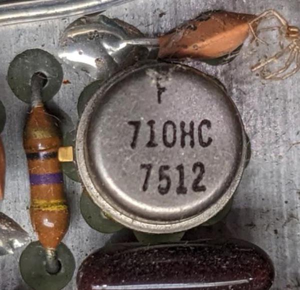
The comparator is a 710HC, a simple differential comparator integrated circuit introduced by Fairchild around 1965. This is one of just two integrated circuits on the board.3 The IC is packaged in an 8-pin circular metal can. This package was common at the time for analog integrated circuits, as the metal can provided shielding.

The 710HC comparator is packaged in a round metal case.

The 710HC comparator is packaged in a round metal case.

Op-amp

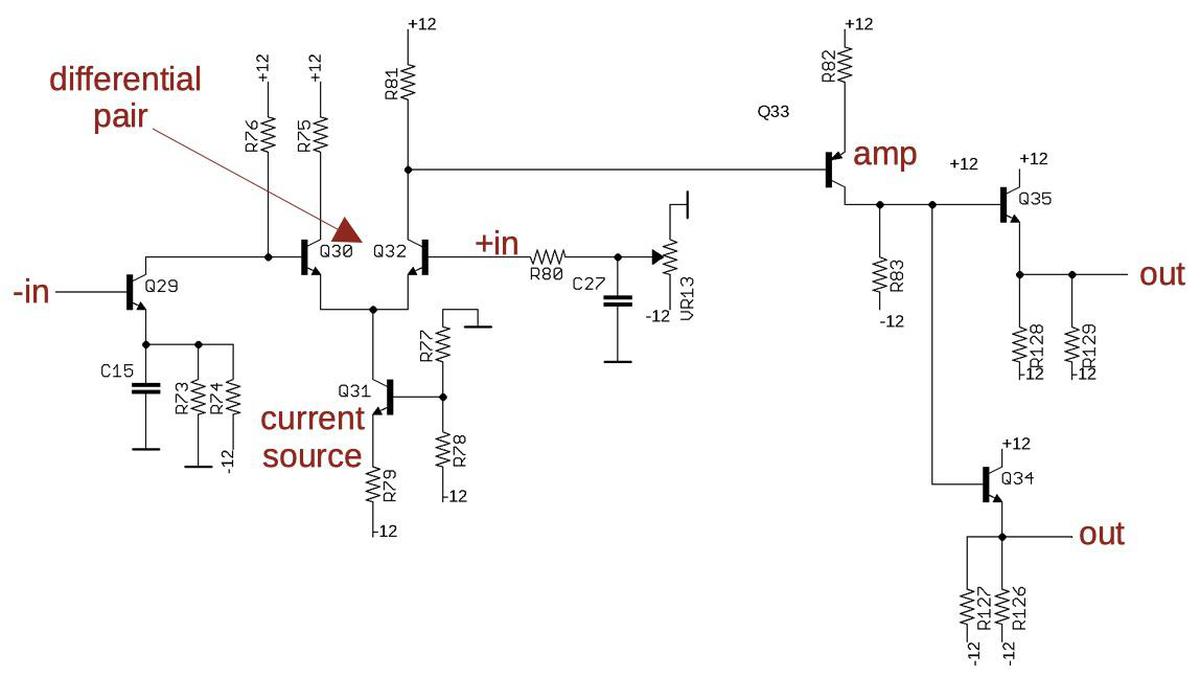
The op-amp is a key component of the integrator. Although integrated-circuit op-amps date back to 1963, this board builds op-amps out of discrete components. The integrator op-amp consists of seven transistors, along with a bunch of resistors and capacitors, as shown below. The heart of the op-amp is the differential pair (Q30 and Q32), a standard analog circuit. A fixed current is fed into the differential pair transistors. If one transistor has a slightly higher input than the other, that transistor turns on and most of the current will go through that transistor. Thus, the differential pair amplifies the difference between the inputs, the key function of an op-amp. Additional amplification is provided by Q33, while Q34 and Q35 buffer the dual outputs.

Implementation of an op-amp in the waveform generator.

Implementation of an op-amp in the waveform generator.

The output amplifier for the waveform circuit uses another discrete op-amp. This one has two stages of differential pairs for additional amplification, followed by power transistors to produce a high-current output. Another op-amp circuit is used in the sine-wave shaper, discussed below.

Sine-wave shaper

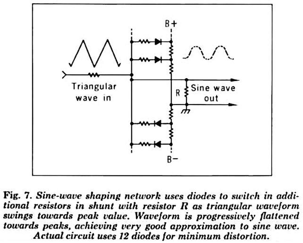
The board uses a surprising technique to generate sine waves: it synthesizes a sine wave from the triangle wave. Specifically, a resistor-diode network shapes the sine wave using piecewise-linear segments. The idea is to use diodes as switches that turn on as the signal level crosses various points. This adds resistance into the circuit, changing the slope. The result is a sine wave with less than 1% distortion.

This diagram explains the sine-wave shaping network. From HP Journal, Nov 1965.

This diagram explains the sine-wave shaping network. From HP Journal, Nov 1965.

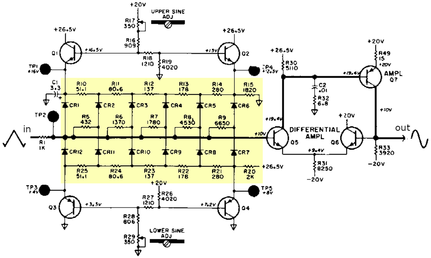
The sine-wave shaper appears to be inspired by the similar circuit in the HP 3300A Function Generator, introduced in 1965. The schematic below shows the HP 3300A's sine-wave shaper; the breadboard's network is similar. The resistances are carefully chosen to achieve the sine wave. Similar resistor-diode networks were also used in analog computers to implement arbitrary functions, sometimes with user-adjustable resistances to change the function.

The sine-shaping circuit from the HP 3300A is very similar to the circuit in the breadboard. The resistor-diode network is highlighted. The surrounding circuitry biases the network and amplifies the output. From the Service Manual Fig 6-2.

The sine-shaping circuit from the HP 3300A is very similar to the circuit in the breadboard. The resistor-diode network is highlighted. The surrounding circuitry biases the network and amplifies the output. From the Service Manual Fig 6-2.

Pulse generator

The pulse generator produces pulses from 100 ns to 100 ms wide. These pulses can be triggered by the waveform generator, an external trigger input, or a "one-shot" pushbutton. The pulse width is controlled by a switch-selectable resistor-capacitor network.

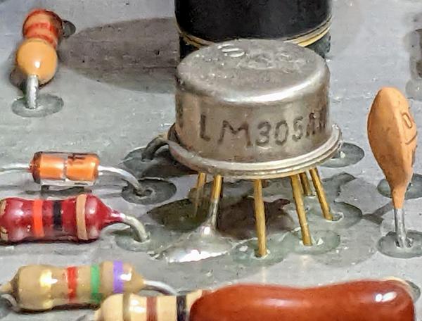
The most unusual part of the pulse generator is how the output circuit adjusts the pulse amplitude. Instead of simply adjusting the amplification, the circuit changes the voltage that powers the output amplifier. This variable voltage is produced by an LM305 voltage regulator IC, adjusted by the amplitude knob on the breadboard. A four-transistor circuit produces the matching negative voltage.4 These voltages power a fairly complex output stage with two circuits. One circuit produces positive pulses, while the other produces negative pulses.

The LM305A integrated circuit is in an old-fashioned metal can.

The LM305A integrated circuit is in an old-fashioned metal can.

Conclusion

A prototyping breadboard may seem like a simple product, but everything becomes more complicated when built with 1969 technology. This breadboard includes a precision waveform generator and power supplies, designed for high accuracy, so it was almost like having test equipment included. But these features came at a steep price, equivalent to $10,000 today.

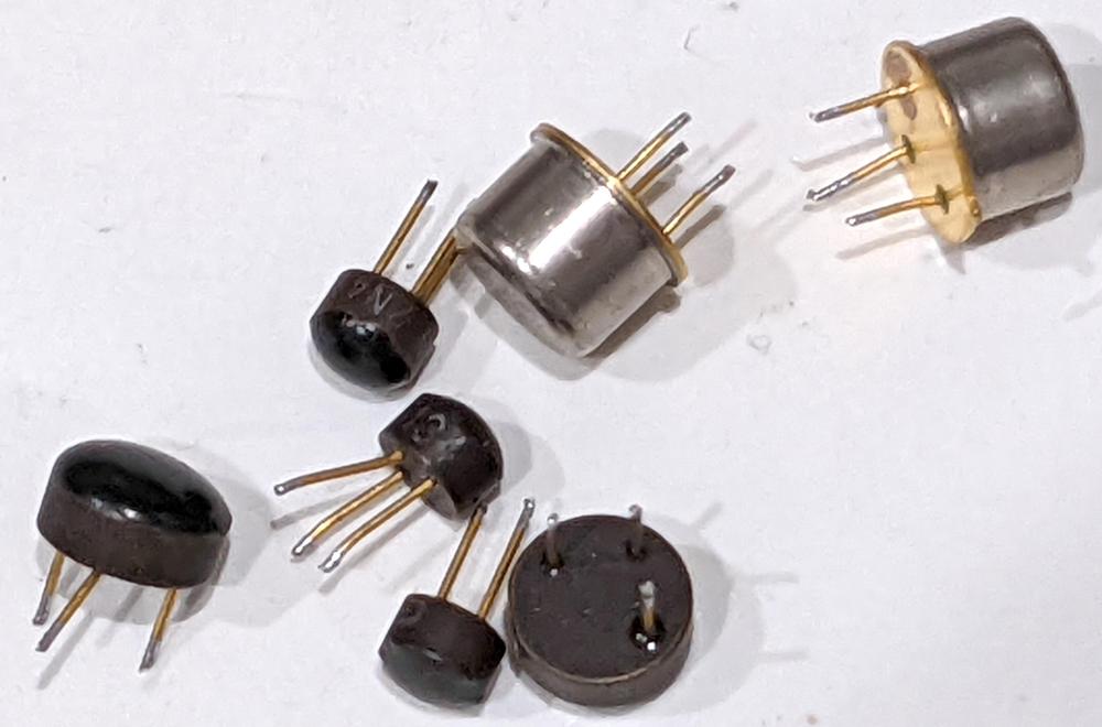
After I reverse-engineered the board,5 CuriousMarc used the schematic to fix the problems. The breadboard turned out to be in bad shape with a broken wire, a bunch of bad transistors, and a failed bridge rectifier in the power supply.6 It's unclear why the board had so many problems, more than you'd expect from age alone. Maybe the power supply over-voltaged the components at some point? My full schematic for the board is here.7

Some of the bad transistors that needed to be replaced.

Some of the bad transistors that needed to be replaced.

CuriousMarc now has a video about the breadboard, so check it out:

Follow me on Twitter @kenshirriff for more posts. I also have an RSS feed.

Notes and references

  1. The breadboard is described in a 1971 brochure

  2. The hysteresis circuit is critical to the stability of the triangle wave. If the comparator input doesn't immediately switch to the lower level at "A", the comparator will switch again as soon as the integrator output drops slightly. Then the integrator will start rising, causing the comparator to switch again. The result is undesired high-speed oscillations (around a megahertz) with the triangle wave remaining stuck. This happened to us while attempting to repair the circuit when we replaced the hysteresis transistor with one that was a bit too slow. 

  3. One unusual feature of the comparator chip is its asymmetrical power supplies. The positive supply (Vcc+) can go up to 14 volts, while the negative supply (Vcc-) is limited to -7 volts. This is inconvenient for the breadboard, which uses ±12 volt supplies internally. The solution is that the breadboard uses a 6.2-volt Zener diode to reduce the negative supply to the chip. R-C filters in the supply lines to the chip reduce noise. 

  4. The negative-voltage circuit produces a negative voltage to match the user-selected positive voltage. In essence, it uses feedback from a resistor voltage divider between the positive and negative rails. When the two voltages are equal (and opposite), the voltage divider will yield 0 volts. If the voltages don't match, the signal from the voltage divider provides feedback to increase or decrease the negative rail as necessary. 

  5. To reverse-engineer the board, I used a process that I've developed recently that works well. I took photos of both sides of the board and used the GIMP software to mirror one image and then align the images using the perspective tool. Next, I created a schematic in EAGLE, putting the symbols in their approximate locations. I wired up the schematic by drawing connections in EAGLE and marking the traces in GIMP as I handled them. The result of this was a "physical" schematic, approximately matching the board's layout.

    The next step was to rearrange the components in EAGLE to create a more logical "functional" schematic. (I find that EAGLE works better than KiCad for this.) This schematic helped me understand how the circuitry was implemented, and we used it to trace through the circuitry and diagnose its problems. 

  6. The breadboard has five different power supplies: three user-adjustable power supplies, and two supplies for internal use, providing unregulated ±32 volts and regulated ±12 volts. Modern systems typically use compact switching power supplies, but the breadboard uses two large and heavy power transformers. Five large power transistors provide regulation, along with massive capacitors. Overall, the power supply illustrates how much power supplies have improved since the 1960s. 

  7. Disclaimer: the schematic isn't completely accurate. In particular, I didn't look up component numbers, so I'm kind of guessing on NPN vs PNP transistors and there are definitely errors. I also didn't record resistor and capacitor values. (The purpose of the schematic was to guide the repairs, not to completely document the device.) 

A look inside the chips that powered the landmark Polaroid SX-70 instant camera

The revolutionary Polaroid SX-701 camera (1972) was a marvel of engineering: the world's first instant SLR camera. This iconic camera was the brainchild of Dr. Edwin Land, a genius who co-founded Polaroid, invented polarized sunglasses, helped design the optics for the U-2 spy plane, and created a theory of color vision. The camera used self-developing film2 with square photos that came into view over a few minutes.3 The film was a complex sandwich of 11 layers of chemicals to develop a negative image and then form the visible color image. But the film was just one of the camera's innovations.

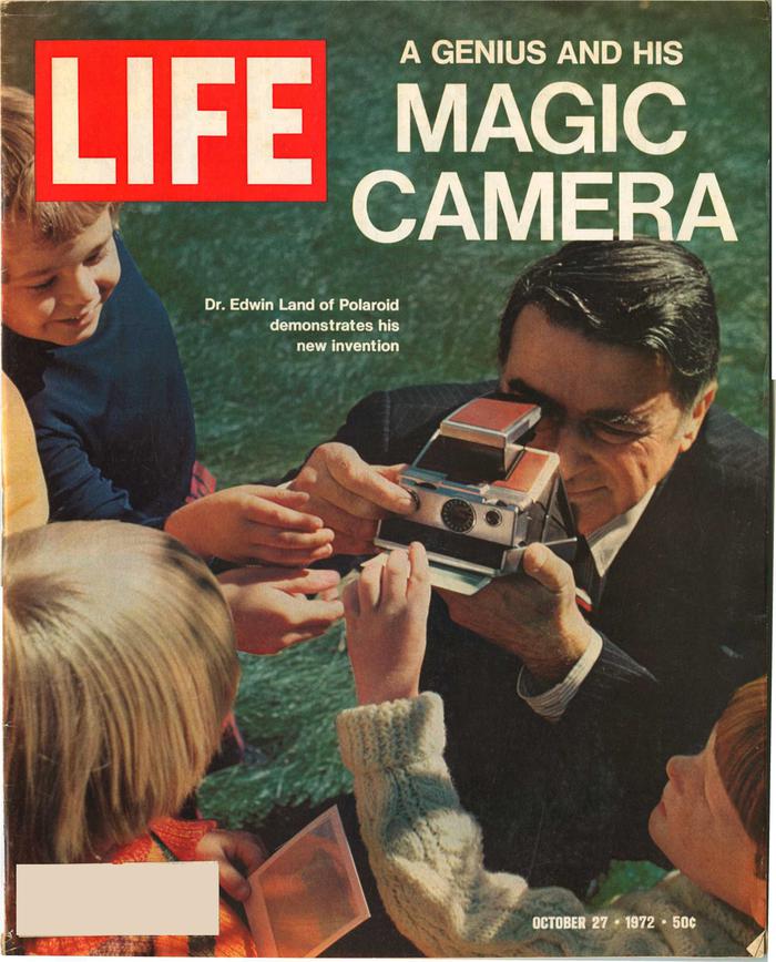
Edwin Land and the Polaroid SX-70 camera were featured on the cover of Life magazine, October 27, 1972.

Edwin Land and the Polaroid SX-70 camera were featured on the cover of Life magazine, October 27, 1972.

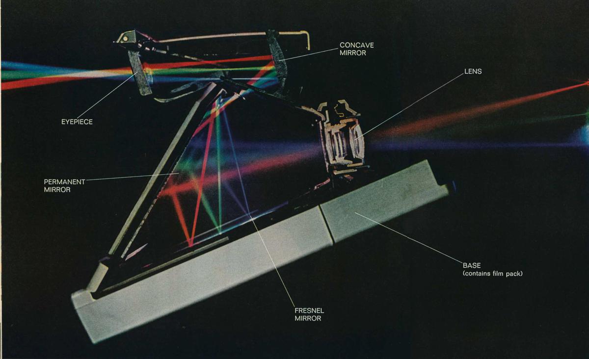
The camera required complex new optics to support the intricate light path shown below. The components included a flat Fresnel mirror, aspherical lenses, and a moving mirror. These optics could focus from infinity down to a closeup of 10 inches. The optics are even more amazing when you consider that the camera folded flat, 3 cm thick and able to fit in a jacket pocket.

Diagram from Life magazine, Oct 1972, showing the light path through the camera.

Diagram from Life magazine, Oct 1972, showing the light path through the camera.

But I'm going to focus on the camera's electronics, powered by a custom flat battery pack. When the shutter button is pressed, the camera carried out several tasks with precision timing. First, a solenoid closes the shutter, blocking the entry of light into the camera. Next, the motor is turned on, causing the camera's internal mirror to flip up to uncover the film. The solenoid is then de-energized, causing the shutter to open. The film exposure time depends on the light level; at the appropriate time, the solenoid closes the shutter again to stop exposure. Finally, the motor runs again to eject the film and reset the mirror.

I'm helping the openSX70 project by reverse-engineering the chips on the exposure control board. This board contains three surface-mount ICs: a chip to read the light intensity from a photodiode, a timer chip to control how long the shutter blades are open, and a power control IC to drive the motor and solenoids.4

The exposure control circuit board, manufactured by Texas Instruments. Photo from openSX70.

The exposure control circuit board, manufactured by Texas Instruments. Photo from openSX70.

The development of this board was contentious, with Fairchild and Texas Instruments battling to supply the electronics for millions of cameras.5 The exposure control board went through three designs as Fairchild and Texas Instruments struggled to meet Polaroid's price target of just $5.75. First, Texas Instruments built a control board from a ceramic substrate with laser-trimmed resistors. The expensive components put the board way over budget at $100 so Polaroid used these boards only in prototype cameras. Fairchild's design was accepted by Polaroid even though its cost of $20 still exceeded the target. Fairchild's board was used from 1972 to 1973, but Texas Instruments fought back with an all-new design that cost only $4.10. This TI board was the long-term winner, and is the one I am examining in this post.

The optical chip

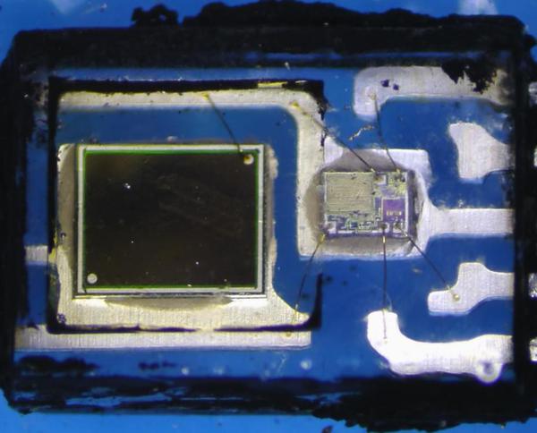
The exposure control board automatically adjusts the exposure time based on the amount of ambient light. Ambient light is measured by the optical chip, a package that combines a photodiode and a silicon die in one small package. The silicon die is protected by epoxy, but the larger photodiode is exposed so external light can fall on it.

The optical chip contains a photodiode and a silicon die in one package.

The optical chip contains a photodiode and a silicon die in one package.

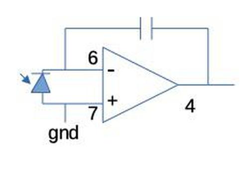
To measure the ambient light, the chip implements the integrator circuit below. The photodiode generates a small current that depends on the light level. This current is integrated over time using a capacitor until a threshold is reached. By opening the shutter during this interval, the film is exposed for the desired amount of time. (The film's exposure depends on the total amount of light received, which is the same value that the integration calculates.) The op-amp die outputs the voltage across the capacitor without draining the capacitor in the process.

The optical chip is essentially an integrator.

The optical chip is essentially an integrator.

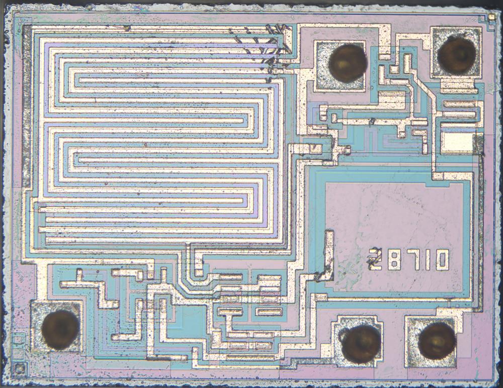
The photo below shows the silicon die under a microscope. The chip, made by Texas Instruments, is dominated by the zig-zags forming two interlocking JFET transistors. A JFET is a special type of transistor, used before MOSFETs became popular. These transistors have very low input currents, so they won't drain the capacitor as it charges. The interlocking layout ensures that both transistors are at the same temperature, so the circuit will stay accurate even if the chip heats up unevenly. The chip also contains NPN and PNP transistors, resistors, and a capacitor (the large pink square labeled 28710).

The optical chip. Photo from siliconPr0n, (CC BY 4.0).

The optical chip. Photo from siliconPr0n, (CC BY 4.0).

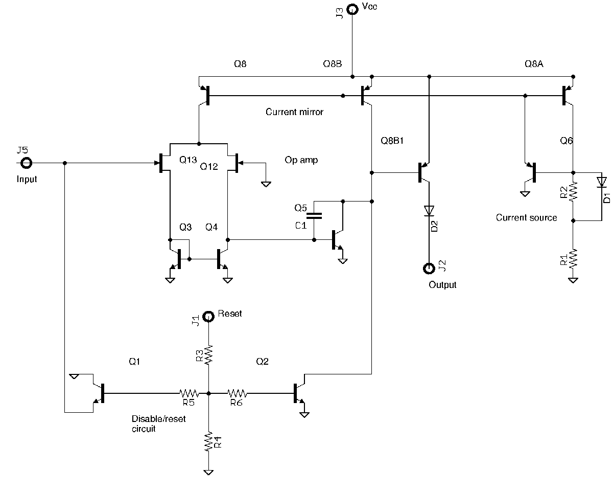
By reverse-engineering the die, I created the schematic below. It is an op-amp, measuring the difference between two inputs (one tied to ground). The two JFET (Q12/Q13) transistors are configured as a standard differential pair circuit. A fixed current (from the current mirror Q8/Q6) is fed into the transistors, and whichever transistor has the higher input will pass almost all the current. The result is amplified by Q5 for the output. In addition to the op-amp circuitry, the chip contains a reset circuit to discharge the capacitor before use (Q1/Q2). (The internal capacitor C1 stabilizes the op-amp; the integration capacitor is external.)

Schematic of the optical chip. Click for a larger version.

Schematic of the optical chip. Click for a larger version.

The power driver chip

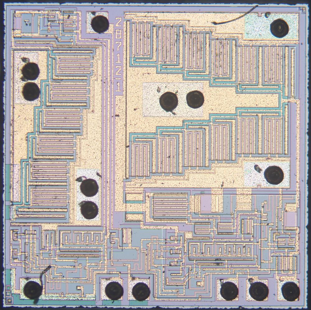
Next, the power chip drives solenoids and the motor to activate the camera's mechanisms. The high-current power transistors (the golden triangular shapes) take up most of this chip. Smaller transistors below form the control circuitry.

The power driver chip. Photo from siliconPr0n, (CC BY 4.0).

The power driver chip. Photo from siliconPr0n, (CC BY 4.0).

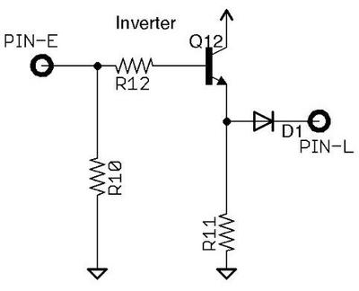
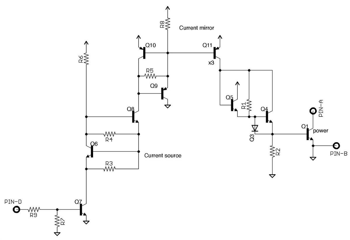
My reverse-engineered schematic shows that the chip has three parts. First, a simple inverter. This probably interfaces the logic chip to the motor control board.

Schematic of the inverter in the power driver chip. Click for a larger version.

Schematic of the inverter in the power driver chip. Click for a larger version.

Second, a high-current driver. This uses the large power transistor at the left of the die. This probably drives a solenoid.

Schematic of the driver in the power driver chip.

Schematic of the driver in the power driver chip.

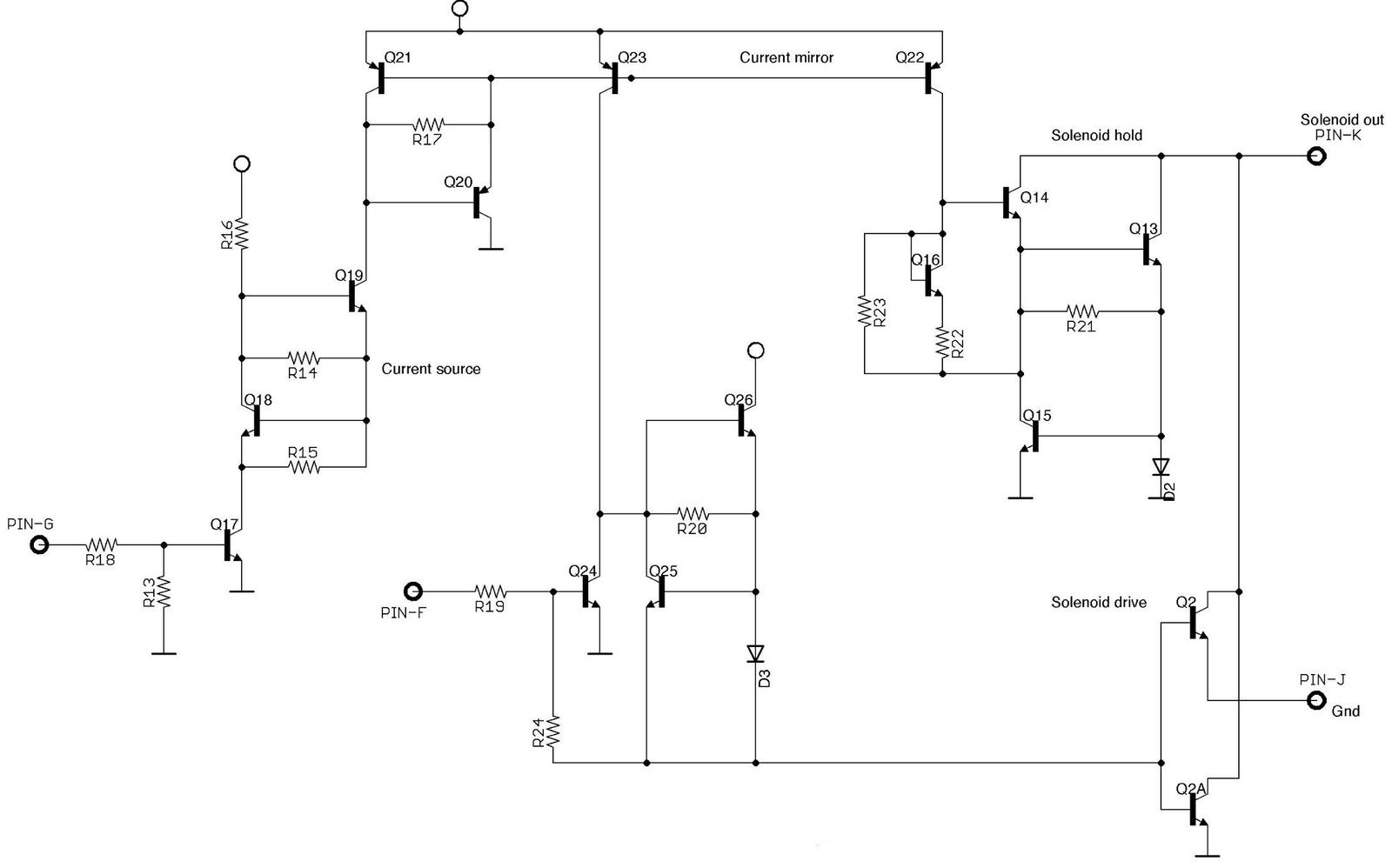
Finally, a high-current driver with a separate circuit for the solenoid hold current. (That is, the solenoid is pulled into position with a high current, and then held in that position with a lower current.) This uses the large power transistors at the right of the die. There's a single large transistor underneath the main "triangle" of transistors; that transistor is for the hold current. This circuit uses separate power and ground pads from the rest of the chip.

Schematic of the driver/hold circuit in the power driver chip.

Schematic of the driver/hold circuit in the power driver chip.

The driver circuits are more complex than I'd expect, using current sources and current mirrors. Maybe this design minimizes standby current use.

The logic chip

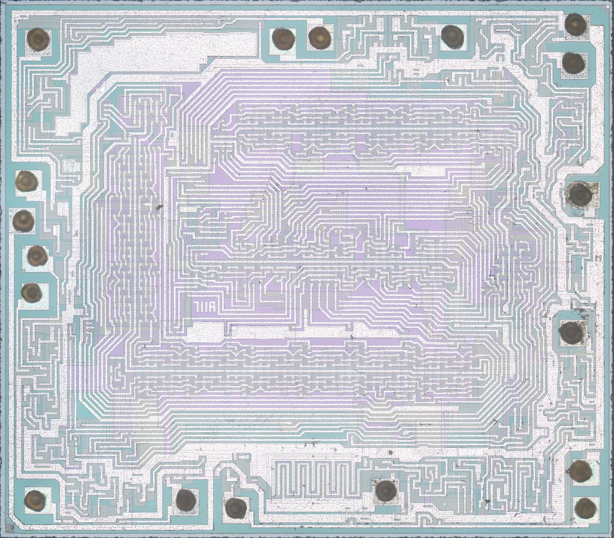
The camera is controlled by a complex logic chip that controlled the timing of the various mechanisms, running the motor and solenoids. It had to handle four different use cases: ejecting the protective cover sheet when a film package was inserted, taking a photo, taking a photo with the flash, and ejecting an empty film package.

This chip was constructed from Integrated Injection Logic (I2L), an obscure 1970s logic family featuring high density and low power. Because the camera ran off a battery in the film pack, minimizing power consumption was a critical factor. At the time, I2L was a good choice for dense, low-power circuitry, although it was soon overtaken by CMOS. Texas Instruments did a lot of development with I2L, including digital watch chips and the 76477 sound chip so it's not surprising that they chose I2L for the camera chip.

The logic chip. Photo from siliconPr0n, (CC BY 4.0).

The logic chip. Photo from siliconPr0n, (CC BY 4.0).

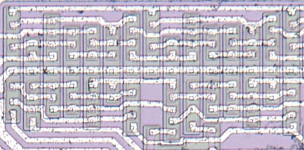
I2L gates can be packed together at high density, as shown below. Each vertical gray rectangle is two transistors (one above the horizontal centerline and one below), corresponding to two gates. The chip has very little wasted space, especially compared to TTL logic, which was commonly used at the time but required multiple transistors and bulky resistors for each gate.

Closeup of the logic chip.

Closeup of the logic chip.

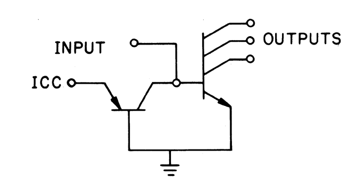
I2L is a bit tricky to understand since an I2L gate has one input and multiple outputs. How can that work? The schematic below shows an I2L gate, with one input and three outputs. Normally the current from the injector (ICC) turns on the output transistor, pulling the output low. But if the input is low, the output transistor turns off and the output will be high. Thus, the gate inverts the input. (You can think of the injector as a pull-up resistor on the input.)

Implementation of an I2L gate. Note that it has a single input and multiple outputs. Icc is the injected current. From "Integrated Injection Logic: A Bipolar LSI Technique".

Implementation of an I2L gate. Note that it has a single input and multiple outputs. Icc is the injected current. From "Integrated Injection Logic: A Bipolar LSI Technique".

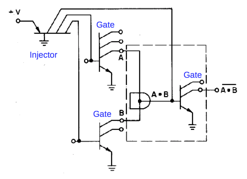
Since the circuit above has a single input, it may seem to be just an inverter. But by wiring several signals together at the input, you get an AND gate "for free": if any signal is low, it will pull the wire low, and otherwise the signal is high. This is called "wired-AND". The wired-AND input to the I2L inverter results in a NAND gate.

One problem arises with wired-AND: if you connect an output to more than one wired-AND, everything gets shorted together. The solution is to have multiple outputs from the inverter. Thus, each I2L NAND gate has a single input and multiple identical outputs. In the diagram below, the outputs from various gates (A and B below) are connected together and fed to the input of an I2L gate, creating a NAND gate.

Diagram of a NAND gate implemented in Integrated Injection Logic (I2L). From "Integrated Injection Logic: A Bipolar LSI Technique".

Diagram of a NAND gate implemented in Integrated Injection Logic (I2L). From "Integrated Injection Logic: A Bipolar LSI Technique".

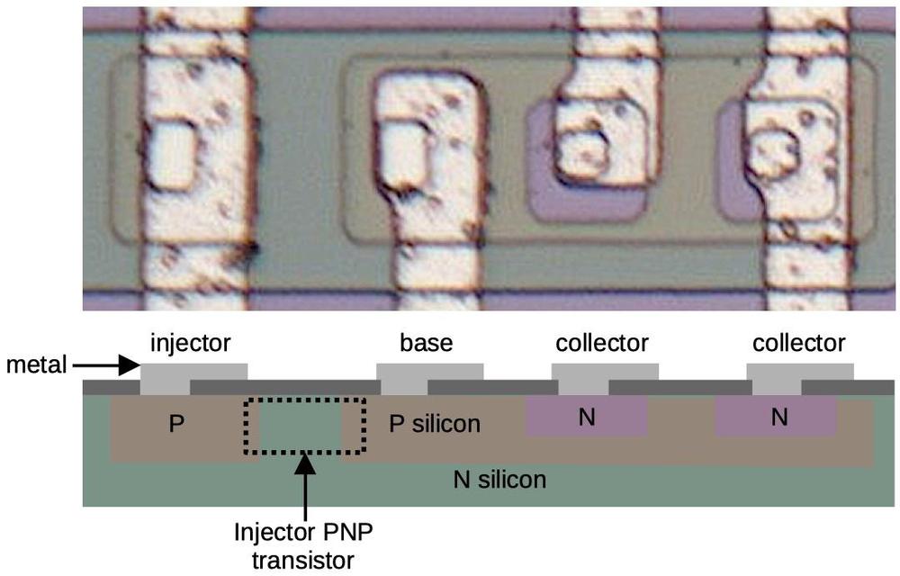
The transistors in I2L have multiple collectors, which may seem strange, but the diagram below shows how they are constructed. Each collector has an N region (purple) with a P region (tan) below for the base, and another N region (green) at the bottom, forming an NPN transistor. The multiple collectors are built by creating multiple N regions. Physically, the injector PNP transistor is just a P region for the emitter, reusing the emitter and base's N and P regions; this makes the injector more compact than a "full" transistor.

Die photo and cross-section diagram of an I2L gate. The transistor base, collectors, and emitters are labeled along with the current injection.

Die photo and cross-section diagram of an I2L gate. The transistor base, collectors, and emitters are labeled along with the current injection.

I haven't reverse-engineered this chip yet. I believe that it contains an oscillator and a chain of flip flops for timing, as well as a comparator for the light level and some miscellaneous control logic.

Conclusion

While the electronics of the SX-70 camera aren't impressive by modern standards, they were cutting edge at the time. They made the SX-70 easy to operate by handling the exposure and timing automatically. Texas Instruments split the electronics across three chips: a precision JFET op-amp with a photodiode, a high-current power driver chip, and a complex logic chip using dense, low-power I2L logic.

Unfortunately, innovative technology wasn't enough for Polaroid. The company declined after competition from Kodak, the expensive failure of the Polavision instant home movie system, and the rise of digital cameras. Polaroid declared bankruptcy in 2001 and the company was broken up. The SX-70 has seen a resurgence in popularity, with film and cameras sold by polaroid.com, which acquired the Polaroid name in 2017.

Follow me on Twitter @kenshirriff for more posts. I also have an RSS feed. Thanks to Joaquín De Prada and Peter Kooiman of openSX70 for providing the chips and John McMaster for decapping them.

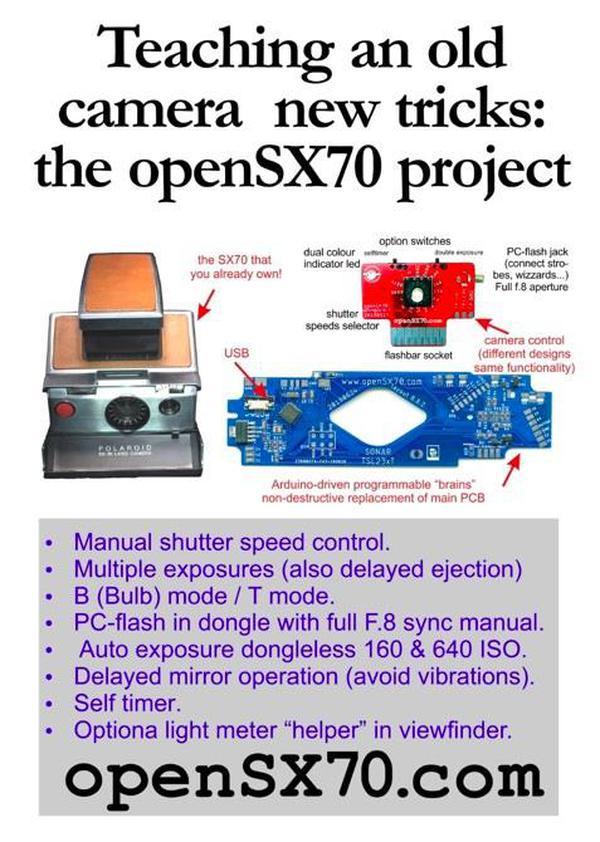
The openSX70 project is building extensions to the SX-70 camera.

The openSX70 project is building extensions to the SX-70 camera.

For more about the SX-70, see the interesting and quirky 10-minute movie below, which markets the SX-70, explains how to use it, and discusses the internal operation. This movie was made in 1972 by the famous designers Ray and Charles Eames.

Notes and references

  1. The name SX-70 comes from its inventor Dr. Edwin Land. He numbered all his "special experiments" in a notebook and his instant picture experiment was number 70. Although the camera was 30 years after special experiment 70, he felt that it embodied the system he had envisioned in the mid-1940s. 

  2. Land introduced instant photography in 1947, and then color instant film in 1963, based on a peel-apart technology. The SX-70 eliminated the problems of the peel-apart instant photos. As Polaroid said, “No pulling the picture packet out of the camera, no timing the development process, no peeling apart of the negative and positive results, no waste material to dispose of, no coating of the print, no print mount to attach, no chance for double exposure, no chance to forget to remove the film cover sheet and spoil a picture, no exposure settings to make, no flash settings to remember, no batteries to replace.”  

  3. Although Polaroid photos develop in a minute or so without any user intervention, shaking the photo was a common custom. "Shaking the Polaroid" was the theme of a 1998 Polaroid ad. Outkast's 2003 song Hey Ya! featured the refrain "Shake it like a Polaroid picture". 

  4. I haven't investigated all the chips in the SX-70. The motor control module contains a linear control IC and power transistors. The camera also takes a flashbar with five flashbulbs. The flash circuit has another chip that checks the bulbs to find an unused bulb. 

  5. "The Battle for the SX-70 Camera", IEEE Spectrum, May 1989 discusses in detail the battle between Fairchild and Texas Instruments to win the Polaroid contract.

    The internal circuitry of the camera is described in "Behind the Lens of the SX-70", IEEE Spectrum, Dec 1973. This circuitry, however, is for the earlier Fairchild version and the implementation is considerably different from the Texas Instruments circuitry that I examined. The Fairchild implementation is also described in "Camera Electronics, A New Approach", WESCON 1973.