How the 8086 processor handles power and clock internally

One under-appreciated characteristic of early microprocessors is the difficulty of distributing power inside the integrated circuit. While a modern processor might have 15 layers of metal wiring, chips from the 1970s such as the 8086 had just a single layer of metal, making routing a challenge. Similarly, clock signals must be delivered to all parts of the chip to keep it in synchronization.

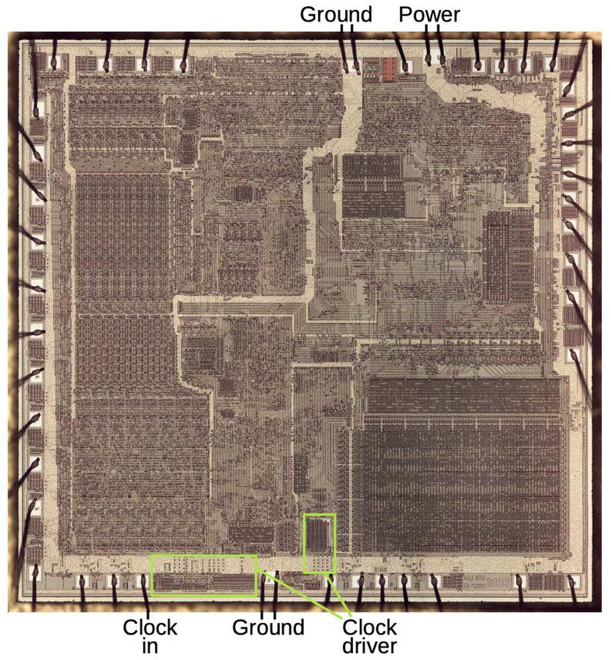
The photo below shows the 8086's die under a microscope. The metal layer on top of the chip is visible, with the silicon substrate and polysilicon wiring hidden underneath. Around the outside of the die, tiny bond wires connect pads on the die to the external pins. The 8086 has a power pad at the top and ground pads at the top and bottom. Each power and ground pad has two bond wires connected to support twice the current. You can see the wide metal traces from the power and ground pads; these distribute power throughout the chip.

Die photo of the 8086 showing power connection (top) and ground connections (top, bottom). The clock circuitry is at the bottom.

Die photo of the 8086 showing power connection (top) and ground connections (top, bottom). The clock circuitry is at the bottom.

Timing in the 8086 is controlled by two internal clock signals. An external oscillator provides a clock signal to the 8086 through the clock input pad at the bottom. The on-chip clock driver circuitry generates two high-current clock signals from this external clock. Note that the clock driver takes up a not-insignificant part of the chip.

In this blog post, I'll discuss how the 8086 routes power and clock signals through the chip, and how the clock driver circuit generates the necessary clock pulses.

Power distribution

The 8086 is constructed with three layers that can be used for wiring. The metal layer on top is best for wiring, since metal has low resistance. Underneath the metal is a layer of polysilicon wiring, made from a special type of silicon. Polysilicon has higher resistance than metal, but can still be used to transmit signals across the chip. The silicon substrate is where the transistors are formed. Silicon has relatively high resistance, so it is only used for short-distance connections, such as inside a gate.

Power routing in a chip like the 8086 creates a topological puzzle of sorts: The metal layer is the only practical layer for routing power and ground, due to its low resistance. Power and ground must be provided to nearly every gate in the chip.1 And since the chip has a single metal layer, power and ground can't cross.

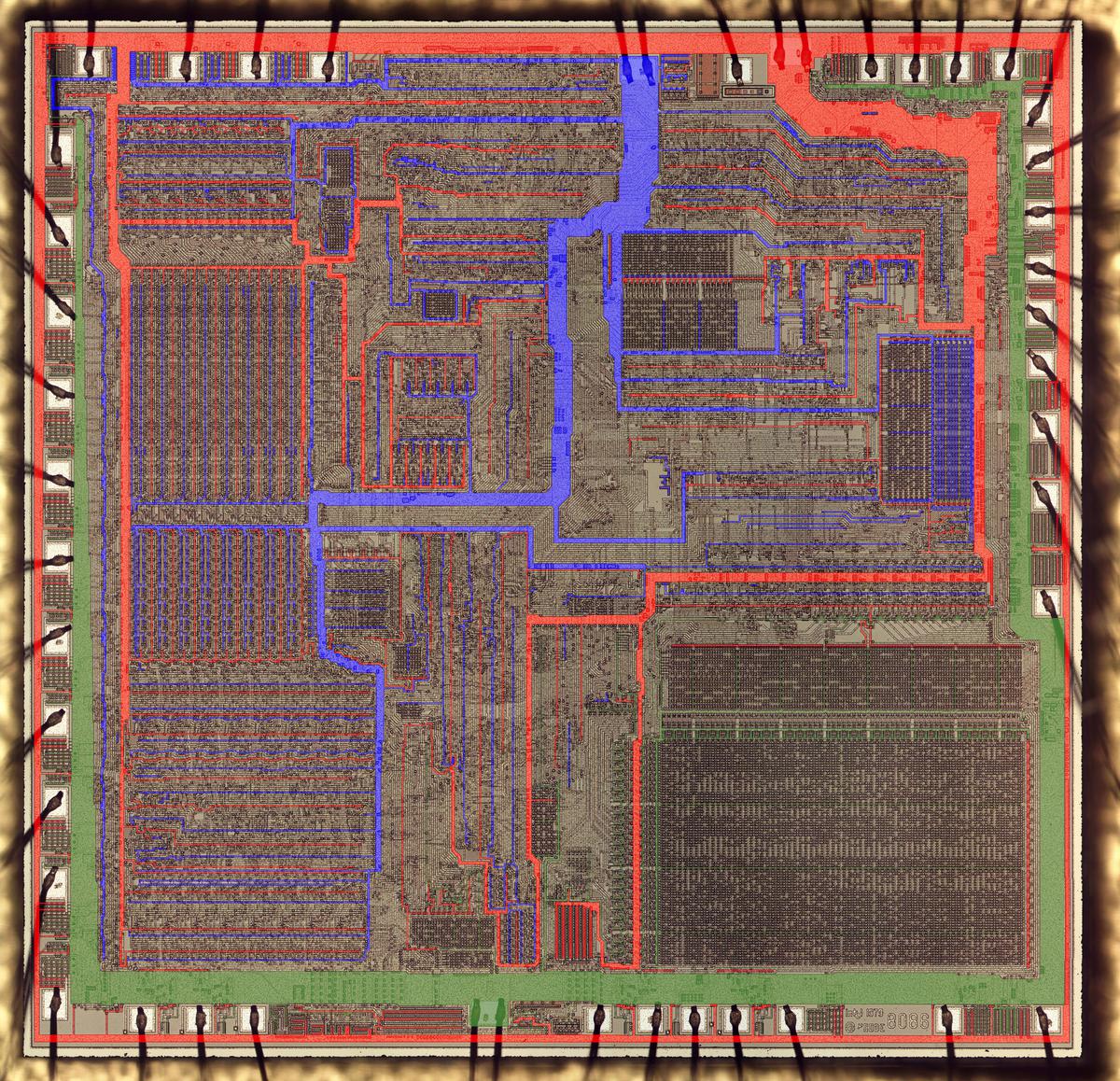
The diagram below highlights these metal wiring networks in the 8086. Power, connected to the power pin at the top, is shown in red, traveling throughout the chip. A major branch flows down and to the right from the power pin, then splitting into multiple paths. Power also travels around the border of the entire chip, supplying the I/O pins.

Power (red) and ground (blue, green) on the metal layer.

Power (red) and ground (blue, green) on the metal layer.

There are two ground pins. The wiring in blue is connected to the upper ground pin, while the wiring in green is connected to the lower ground pin. The blue ground wiring has a large branch downwards through the center of the chip, branching in complex directions. The green ground wiring flows along the bottom, left, and right sides of the chip, supporting the I/O pins, as well as connected to the microcode ROM in the lower right.

The power wires get thinner from their source to their final destination as they branch or deliver power along the way and the current diminishes. This is visible in the ground wire to the address / data pins, below. At the left, the ground wire below the pins is very wide, but it tapers off to the right. In other words, at the left, the wire must handle current for all the pins, but at the right the wire is supporting just the remaining pin.

The ground connection to the Address/Data pins gets progressively thinner. (Left side of chip, rotated 90°)

The ground connection to the Address/Data pins gets progressively thinner. (Left side of chip, rotated 90°)

The metal layer is used for many signals besides power and ground; it is the best layer for delivering signals due to its low resistance. However, the extensive power and ground wiring constrains the other uses of the metal layer. To avoid intersections, most of the metal signal lines run parallel to the power lines; the polysilicon layer underneath is used to run perpendicular signals. But what happens if metal wires need to cross a power or ground line? The solution is to use a "crossunder", where the signal goes down to the polysilicon layer and crosses under the power line, popping back up on the other side,3 as shown below.

Signals in the metal layer crossing under the power line by using polysilicon crossunders.

Signals in the metal layer crossing under the power line by using polysilicon crossunders.

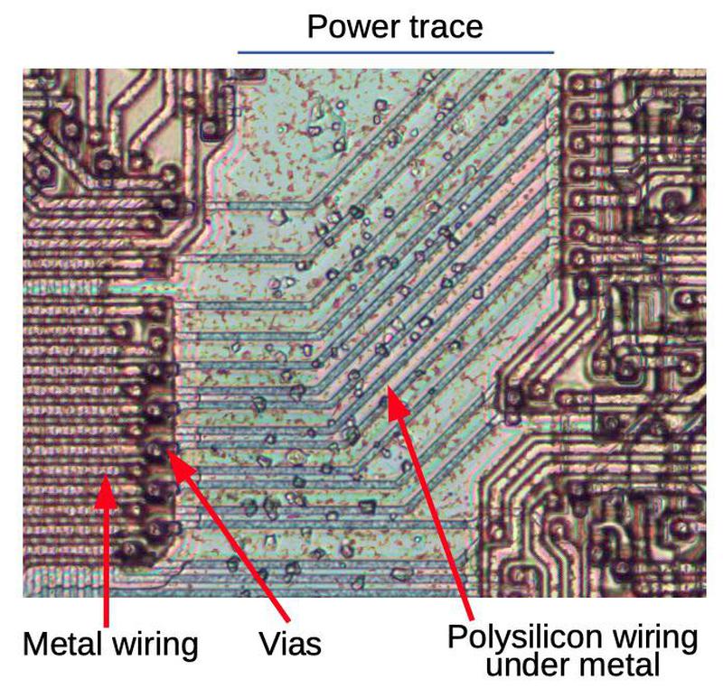
While power and ground are almost entirely routed in the metal layer, there are a few places where this breaks down and a crossunder is used for power. This typically happens near the end of the line, where the current is small. One example is shown below, where ground passes through two polysilicon crossunders. To reduce the resistance, these crossunders are much wider than the crossunders for signals and also use the silicon and polysilicon layers together. The small circles are connections (called vias) between the metal layer and the polysilicon layer.

Composite photo showing polysilicon crossunders for ground that pass under signal lines.

Composite photo showing polysilicon crossunders for ground that pass under signal lines.

The silicon layer plays a minor part in routing power. In particular, many gates are stretched out to reach the power and ground on either side. The photo below shows some gates in the 8086. Note the large doped silicon regions (white) that extend to reach the power and ground lines. Only a small part of this silicon is used for transistors, while the rest looks like wasted space. However, these empty silicon regions connect the gate to the metal power and ground wires. Since silicon has relatively high resistance, wide regions are used for these connections, and over short distances.

The doped silicon forming gates can be extended to reach the power and ground lines. The metal layer was removed for this photo so the power and ground lines are illustrated.

The doped silicon forming gates can be extended to reach the power and ground lines. The metal layer was removed for this photo so the power and ground lines are illustrated.

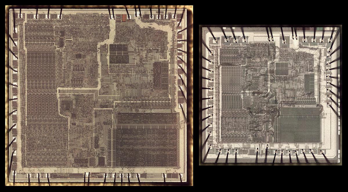
Other power routing issues arose as the 8086 was revised and became physically smaller. As manufacturing technology improved, Intel performed "die shrinks", keeping the same circuitry but scaling it down uniformly to produce a smaller die. Unfortunately, shrinking the power lines reduces the current they can handle. The solution was beef up the power lines around the edge of the chip, while allowing the internal circuitry and wiring to shrink. This can be seen in the photo below; the lower-right corner of the smaller 8086 has much more power wiring, for instance. (I wrote more about the 8086 die shrink here.)

Two versions of the 8086 die, at the same scale. The die on the right is a later version of the 8086, reduced in size.

Two versions of the 8086 die, at the same scale. The die on the right is a later version of the 8086, reduced in size.

The processor clock

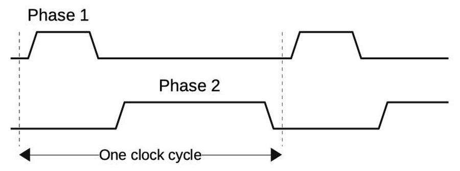
Almost all computers use a clock signal to control the timing of the processor.4 Like many microprocessors, the 8086 uses a two-phase clock internally.5 In a two-phase clock, there are two clock signals: when the first clock is high, the second is low, and vice versa, as shown below. One set of circuitry is enabled by the first clock, while a second set of circuitry is enabled by the second clock. The 8086's circuitry requires that the two clock phases are non-overlapping —there is a gap after one goes low before the other goes high—and asymmetrical.6

A two-phase clock consists of two clock signals with opposite polarity.

A two-phase clock consists of two clock signals with opposite polarity.

In modern processors, clock routing is complex because the clock signals must reach all parts of the chip at the same time. Modern processors use a hierarchy of clock paths, balancing the time along each path, and often provide separate buffering for each path. In comparison, the 8086's clock routing is straightforward because its 5 to 10 MHz clock7 is orders of magnitude slower than modern processors. At these comparatively low speeds, the length of the path doesn't make much difference, so the 8086's clock signals can meander around the chip.

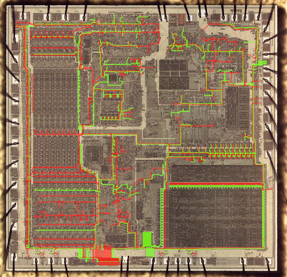
Clock routing in the 8086. Green is clock while red is the opposite phase clock.

Clock routing in the 8086. Green is clock while red is the opposite phase clock.

The diagram above shows the 8086's clock routing. Phase 1 is in green and phase 2 is in red. At the bottom of the chip, the circuitry that generates the clocks appears as large blobs. From there, the clock signals branch wind around the chip. For the most part, the two clock phases are routed parallel to each other, unlike power and ground, which form opposing branches.

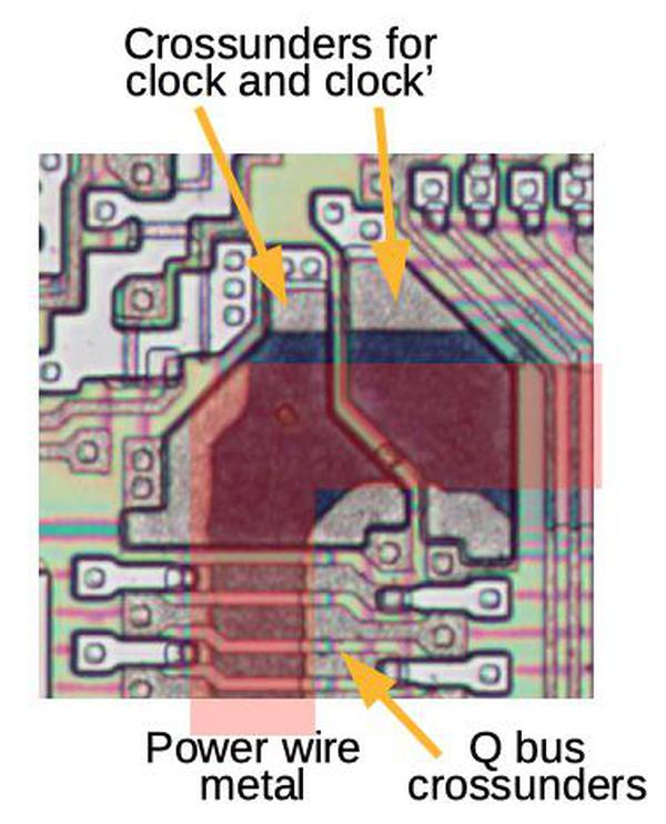
Because the clock signals go to all parts of the chip, they require much more current than typical signals and are routed in the metal layer for the most part. When the clock signals must cross the power lines, they use large crossunders as shown below. Note that the irregularly-shaped clock crossunders are much larger than the crossunders for other signals, such as the Q bus below.

The clock has large crossunders to cross the power wire. The Q bus (which transfers instructions from the instruction queue to the decoder) has much smaller crossunders.

The clock has large crossunders to cross the power wire. The Q bus (which transfers instructions from the instruction queue to the decoder) has much smaller crossunders.

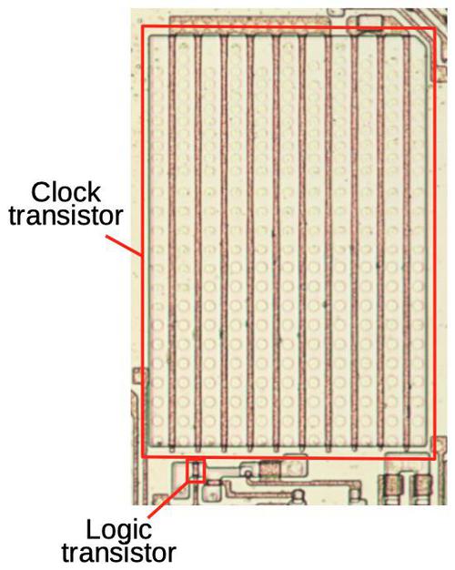
To provide the high-current clock signals, the clock signals have special driver circuitry built from large transistors. The photo below compares one of these driver transistors to a typical logic transistor. The driver transistor is about 300 times as large, so it can provide about 300 times the current. This transistor is constructed as 10 transistors in parallel; the 10 vertical polysilicon lines form the 10 gates. Each clock signal is driven by a pair of large transistors, one to pull the signal high and one to pull the signal low.

A large transistor in the clock driver compared to a neighboring logic transistor.

A large transistor in the clock driver compared to a neighboring logic transistor.

The photo below shows the clock driver circuitry. This circuit splits the external clock signal into two phases, makes the phases non-overlapping, and amplifies them. At the left, the pink square is the pad for the externally-supplied clock. The signal passes through a series of transistors, ending with the large driver transistors at the right for the clock signal. The brownish wiring is the polysilicon that forms the gates. Many transistors have zig-zagging gates to fit a larger transistor into the available space.

The clock driver circuitry on the die. The metal has been removed, revealing the large transistors in the circuit. The clock input pin is the purple square on the left.

The clock driver circuitry on the die. The metal has been removed, revealing the large transistors in the circuit. The clock input pin is the purple square on the left.

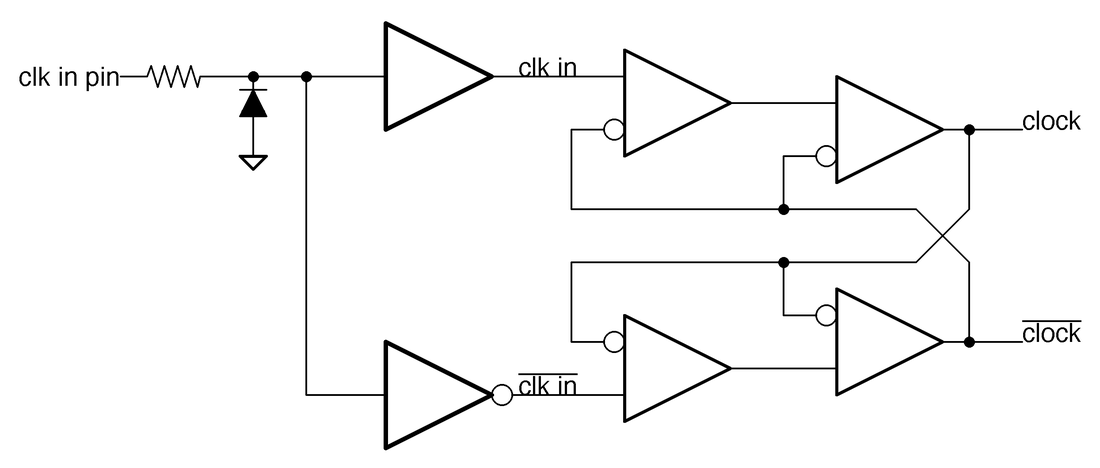
The schematic below shows the driver circuitry, slightly simplified. The triangles indicate high-current drivers, built from two or three transistors; an inverting input (indicated by a bubble) pulls the output low. At the left, the clock input pin has a small resistor and a diode to provide some protection (like the other input pins). Next, the clock is split into an uninverted phase (top) and an inverted phase (bottom).

Simplified schematic of the clock driver circuitry in the 8086.

Simplified schematic of the clock driver circuitry in the 8086.

The additional circuitry keeps the clocks from overlapping: when one clock is high, it forces the other side low, through the inverted inputs. To see how this works, let's start with the clk in pin high, so clk in and clock are high while clk in and clock are low. Now, suppose the clk in pin input goes low, causing clk in to go low and clk in to go high. However, the output clock can't go high until clock goes low, due to the negative inputs on the buffers. Once that happens, clk in proceeds through the lower drivers, pulling clock high after two gate delays.8 The point of this is that clock and clock don't switch at the same time; after one goes low, there is a delay before the other goes high. This generates the desired non-overlapping clock signals.

Conclusions

The 8086 uses some interesting routing for power, but modern processors operate at a whole different level. While the 8086 required 350 milliamps of current, a modern processor might require over a hundred amps. The 8086 used 3 of its 40 pins for power and ground, compared to a modern Intel Core i5 processor with 128 power pins and 377 ground pins (out of 1151 pins). Although the numerous metal layers in modern chips solved the 8086's routing issues, modern chips have new complications such as multiple power domains that allow unused parts of the chip to be powered down.

Clock routing is much harder on modern processors since at multi-gigahertz speeds, even an extra millimeter of path can affect the clock. To deal with this, modern processors use techniques such as H-trees or grids to distribute the clock, rather than the 8086's meandering paths. While the 8086 has a simple circuit to generate the two-phase clock, modern processors often use a phase-locked loop (PLL) to synthesize the clock and use multiple circuits scattered across the chip to generate and control clock signals.

Even though the 8086 is much simpler than modern processors, it contains a lot of interesting circuitry. I plan to reverse-engineer more of the 8086, so follow me on Twitter at @kenshirriff for updates. I also have an RSS feed.

Notes and references

  1. Power and ground must be provided to almost every gate in the chip since a standard NMOS gate requires ground for its pull-down network and power for its pull-up resistor. There are a few exceptions, though. The 8086 uses some dynamic logic gates, especially in the ALU for speed. These gates are pulled high by the clock, so they don't need a direct power connection. The 8086 also uses some pass-transistor XOR gates, which are pulled low by the inputs, so they don't need ground.

    The microcode ROM forms a large region with no power connections, just ground. This is because each row in the ROM is implemented as a very large NOR gate with the power pull-up on the right-hand edge. Thus, the ROM gates all have power and ground, even though it looks like the ROM lacks power connections. 

  2. Integrated circuits often have power and ground on opposite corners or opposite sides of the chip. This placement makes it easier to construct the non-intersecting power and ground networks in the chips. The 8086 is slightly unusual to have power and ground on diagonally-opposite pins, but then a second ground pin close to the power pin. The solution is to have tree-like branching networks for power and ground. These networks are interdigitated, meshed like fingers to reach all parts of the chip.2 

  3. Crossunders are used for many wire crossings, not just power, but power wiring is a key contributor. Typically, metal wiring is used for signals in one direction, while polysilicon wiring is used for signals in the perpendicular direction. (These directions vary in different parts of the chip, depending on the predominant direction for signals.) Thus, signals for the most part can travel unimpeded. Even so, signals often bounce from layer to layer to make the routing work. 

  4. While almost all computers are synchronous and operate with a clock, the IAS machine architecture (popular in the 1950s) was asynchronous, operating without a clock. Instead, each circuit would send a pulse to the next when it was done, triggering the next step. Many early computers of the 1950s were based on the IAS machine architecture, including CYCLONE, ILLIAC, JOHNNIAC, MANIAC, SEAC, and the IBM 701. Research into asynchronous computing continues (link, link), but synchronous designs are dominant. 

  5. Among other things, processors use the clock to prevent unwanted feedback in the circuitry. For instance, consider a program counter with a circuit to increment it and feed the result back to the program counter. You don't want the new value to get repeatedly incremented.

    One approach is to use edge-sensitive circuits (flip flops) that will update that value in the program counter at the moment the clock goes high. Thus, there will be a single update as desired. However, with a two-phase clock, the circuit can be built from level-sensitive latches, which are much simpler than edge-sensitive flip flops. The idea is that when the first clock is high, the first half of the circuit receives input and does its logic calculations When the second clock is high, the second half of the circuit receives input from the first half and does any necessary calculations, while the first half is blocked. The point is that only half of the circuitry can update at any time, preventing uncontrolled feedback. 

  6. The 8086 has strict requirements on its input clock, which must be high for 1/3 of the time. The clock signal into the 8086 was typically produced by an 8284 chip and a quartz crystal. This chip divided its input clock by 3 to generate the 33% duty cycle clock required by the 8086.  

  7. Because the 8086 used dynamic logic, it also had a minimum clock speed of 2 MHz. If the clock ran slower than this, there was a risk of charges leaking away before they were refreshed, causing failures. The minimum clock speed was inconvenient for debugging, since you couldn't slow down or stop the clock. 

  8. This is a somewhat handwaving description of the clock driver circuit. In particular, I'm not sure what happens when one transistor is pulling a signal high and another is pulling the same signal low. An accurate simulation would depend on the relative sizes of the two transistors. 

Latches inside: Reverse-engineering the Intel 8086's instruction register

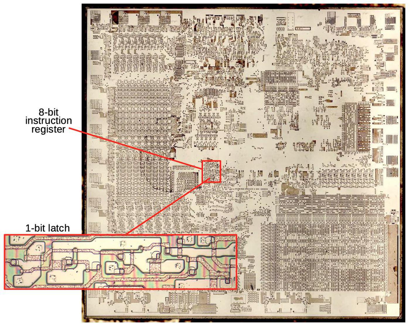
The Intel 8086 microprocessor is one of the most influential chips ever created; it led to the x86 architecture that dominates desktop and server computing today. But it is still simple enough that its circuitry can be studied under the microscope and understood. In this post, I explain the implementation of a dynamic latch, a circuit that holds a single bit. The 8086 has over 80 latches scattered throughout the chip, holding a variety of important processor state bits,1 but I'll focus on the eight latches that implement the instruction register and hold the instruction that is being executed.

The 8086 die, showing the 8-bit instruction register.

The 8086 die, showing the 8-bit instruction register.

The photo above shows the silicon die of the 8086 processor under a microscope. I removed the metal and polysilicon layers to reveal the transistors, approximately 29,000 of them. The highlighted region indicates the 8086's 8-bit instruction buffer, consisting of eight latches. (This 1978 processor is simple enough that a single 8-bit register occupies a substantial region of the die.) The closeup shows the silicon and transistors making up a single latch.

The dynamic latch and how it works

The latch is one of the most important circuits in the 8086, since the latches keep track of what the processor is doing. While latches can be made in many ways,2 the 8086 uses a compact circuit called the dynamic latch. The dynamic latch depends on a two-phase clock, commonly used to control microprocessors of that era.3 A two-phase clock consists of two clock signals that are active in alternation. In the first phase, clock is high and the complement clock is low. Then they switch so clock is low and clock is high. This cycle repeats at the clock frequency, such as 5 MHz.

A latch in the 8086 processor is built from four pass transistors and two inverters. The latch runs off the alternating clock signals. The control signals are load and hold.

A latch in the 8086 processor is built from four pass transistors and two inverters. The latch runs off the alternating clock signals. The control signals are load and hold.

The schematic above shows a typical latch in the 8086. It consists of two inverters and several pass transistors. For our purposes, the pass transistor can be considered a switch: if the gate input is 1, the transistor passes the signal through. If the gate input is 0, the transistor blocks the signal. The pass transistors are controlled by several signals: load, which loads a bit into the latch; hold, which holds the existing bit value; clock, the first clock phase; and clock, the second, inverted clock phase.

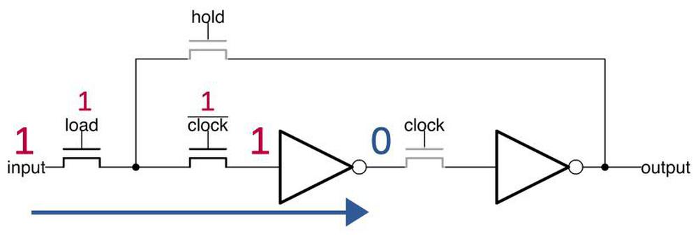
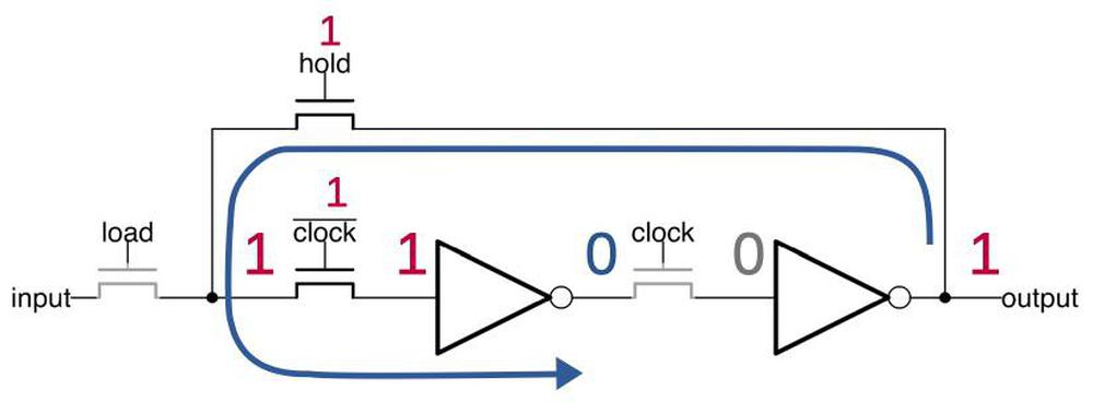
The diagram below shows how a value (1 in this case) is loaded into the latch. The load signal is brought high, allowing the input (1 in this example) to pass through the first transistor. Since clock is high, the signal passes through the second transistor to the inverter, which outputs 0. At this point, the third (clock) transistor blocks the signal.

The input is loaded into the latch when the load signal is high.

The input is loaded into the latch when the load signal is high.

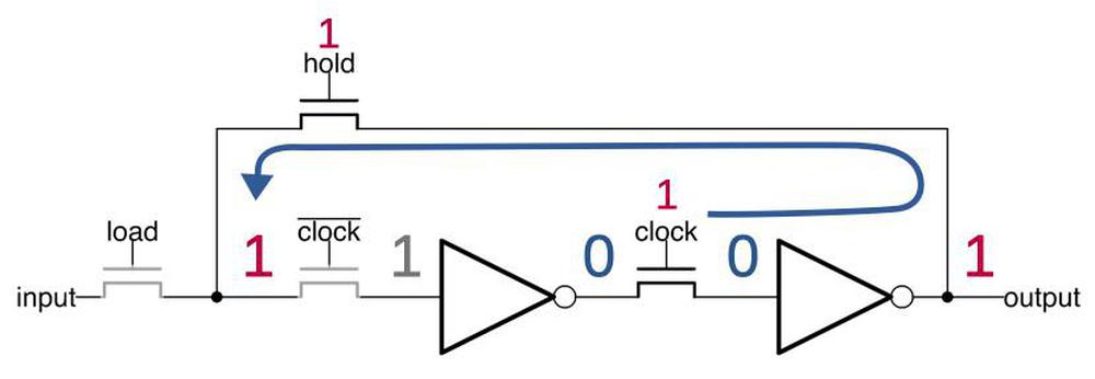
In the next clock phase (below), clock goes high, allowing the 0 signal to reach the second inverter, which outputs 1. Since hold is high, the signal loops back, but is blocked by the clock transistor. The important point, which makes this circuit dynamic, is that at this time there is no active input to the first inverter. Instead, its input remains 1 (shown in gray) due to the capacitance of the circuit. Eventually, this charge would leak away, losing the value, but before that happens, the clocks toggle.

When clock is high, the value passes through the second inverter. The (grayed-out) input to the first inverter is maintained by the circuit's capacitance.

When clock is high, the value passes through the second inverter. The (grayed-out) input to the first inverter is maintained by the circuit's capacitance.

After the clocks switch state, the second inverter's input is provided by the capacitance of the circuit (below). The signal loops around, recharging and refreshing the input to the first inverter. As the clock signals continue to toggle, the latch switches between this diagram and the previous diagram, preserving the value in the latch and keeping the output stable.4

When
clock
is high, the value passes through the first inverter.

When clock is high, the value passes through the first inverter.

The implementation in silicon

The 8086 and other processors of that era were built from a type of transistor called NMOS. They were constructed from a silicon substrate that was "doped" by diffusion of arsenic or boron to form the transistors. On top of the silicon, polysilicon wiring created the gates of the transistors and wired components together. Finally, a metal layer on top provided more wiring. (In comparison, modern processors are built from CMOS technology, which combines NMOS and PMOS transistors, and they have many layers of metal wiring.)

Structure of an NMOS transistor (MOSFET) as implemented in an integrated circuit.

Structure of an NMOS transistor (MOSFET) as implemented in an integrated circuit.

The diagram above shows the structure of a transistor. The transistor can be viewed as a switch, allowing current to flow between two diffusion regions called the source and drain. The transistor is controlled by the gate, made of a special type of silicon called polysilicon. Applying voltage to the gate lets current flow between the source and drain, while pulling the gate to 0 volts blocks the current flow. The gate is separated from the silicon by an insulating oxide layer; this makes the gate act like a capacitor as seen in the dynamic latch.

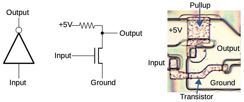
An inverter (below) is built from an NMOS transistor and a resistor.5 With a low input, the transistor is off, so the pull-up resistor pulls the output high. With a high input, the transistor turns on. This connects the output to ground, pulling the output low. Thus, the circuit inverts the input signal.

This schematic shows how an inverter is created from a transistor and resistor. The photo shows the implementation inside the chip.
The metal layer was removed to show the polysilicon and silicon underneath.

This schematic shows how an inverter is created from a transistor and resistor. The photo shows the implementation inside the chip. The metal layer was removed to show the polysilicon and silicon underneath.

The photo on the right shows how an inverter is physically constructed in the 8086. The yellowish regions are conductive doped silicon and the speckled regions are the polysilicon on top. A transistor is created where polysilicon crosses doped silicon: the polysilicon forms the transistor's gate, while the silicon regions on either side are the transistor's source and drain. The large polysilicon rectangle forms the pull-up resistor between +5 volts and the output. These physical structures can be matched with the schematic.

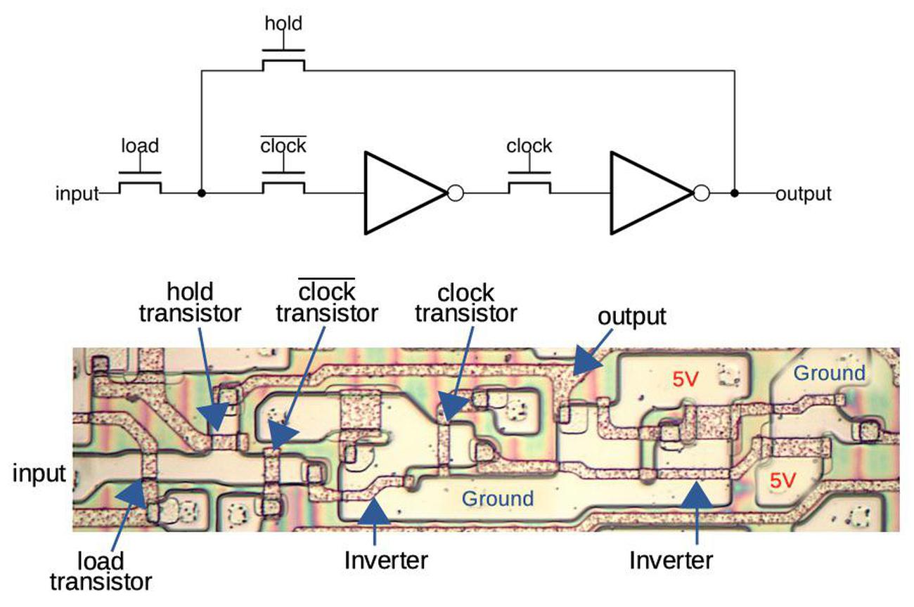
The diagram below shows the implementation of a latch on the chip. The pass transistors and the two inverters are indicated; the first inverter is the one described above. Polysilicon wiring connects the components together; the metal layer (removed) provided additional wiring. The transistors have complex shapes to make the most efficient use of the space.

Microscope photo of a latch in the 8086 processor. The metal wiring was removed, but traces remain as reddish vertical lines. Note: this photo is rotated 180° to match the schematic.

Microscope photo of a latch in the 8086 processor. The metal wiring was removed, but traces remain as reddish vertical lines. Note: this photo is rotated 180° to match the schematic.

The latch includes output buffers, not shown on the schematic above, that provide high-current signals for the output and inverted output. This type of buffer has the amusing name "superbuffer" because it provides much higher current than a regular NMOS inverter. The problem with an NMOS inverter is it is slow when driving something with high capacitance. Since the superbuffer provides more current, it will switch the signal much faster. The superbuffer accomplishes this by replacing the pullup resistor with a transistor, which provides higher current. The downside is that the pullup transistor requires an inverter to drive it, so the superbuffer circuit is more complex. Thus, superbuffers are only used when necessary, typically when sending a signal to many gates or when driving a long bus line.

Superbuffer implementation in the 8086's latch.  Note that the +5V and ground connections are switched on the rightmost transistors.

Superbuffer implementation in the 8086's latch. Note that the +5V and ground connections are switched on the rightmost transistors.

The diagram above shows the superbuffer circuit in the 8086's latches. Unlike the typical superbuffer, this one includes both an inverting and non-inverting superbuffer. To understand the circuit, note that the central resistor and transistor form an inverter. The inverter output is connected to the upper transistors, while the uninverted input is connected to the lower transistors. Thus, if the input is 1, the lower transistors will turn on, while if the input is 0, the upper transistors will turn on due to the inverter. Thus, for a 1 input, the lower transistors will pull Output high and the complement Output low. But for a 0 input, the upper transistors will pull Output low and the complement Output high.6

The instruction register

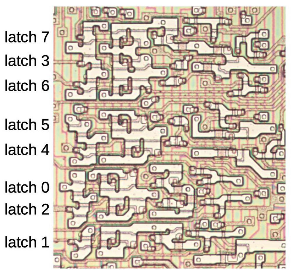
The 8086, like most processors, has an instruction register that holds the instruction that is currently being executed. In the 8086, the instruction register holds the first byte of an instruction (which may consist of multiple bytes), so it is built from eight latches (below). You might expect the latches to be identical, but each latch has a different shape. Since the layout of the 8086 is highly optimized, each latch is shaped to make the best use of the available space, constrained by the neighboring wiring. In particular, note that some latches are merged together so they can share power and ground connections. Layout optimization is also probably why the latches are not in sequential order.

The 8 latches all have somewhat different shapes, optimized for the wiring around them.
The previous sections described latch 1, rotated 180° from this photo.
The red vertical lines are traces of the removed metal layer.

The 8 latches all have somewhat different shapes, optimized for the wiring around them. The previous sections described latch 1, rotated 180° from this photo. The red vertical lines are traces of the removed metal layer.

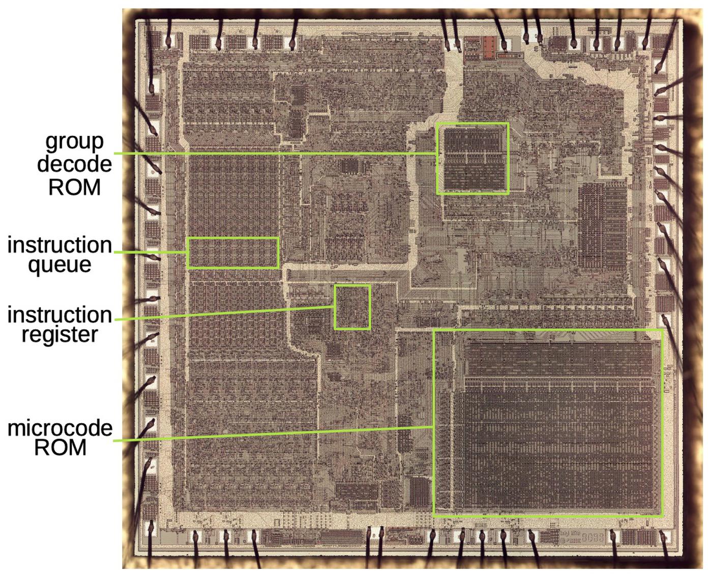
An instruction takes a winding journey through the 8086 chip. The 8086 processor uses prefetching, improving performance by loading instructions from memory before they are required. Prefetched instructions are stored in the instruction queue, a 6-byte queue in the middle of the 8086's register file. (In comparison, modern processors can have megabytes of instruction cache.) When an instruction is executed, it is stored in the instruction register, roughly in the middle of the chip. (The relatively large distances explains the use of superbuffers.) The instruction register feeds the instruction to the "group decode ROM". This ROM determines the high-level characteristics of the instruction, such as if it is a single-byte instruction, a multi-byte instruction, or an instruction prefix. (This is only a piece of the 8086's complex instruction handling. Other latches hold pieces of the instruction indicating register usage and the ALU operation, while a separate circuit controls the microcode engine, but I'll discuss that in another post.)

The 8086 die, showing key pieces for instruction processing. Around the outside of the die, bond wires connect the die to the external pins.

The 8086 die, showing key pieces for instruction processing. Around the outside of the die, bond wires connect the die to the external pins.

Conclusions

The 8086 makes extensive use of dynamic latches to store state internally. These latches are visible under a microscope and their circuitry can be traced out and understood. The 8086 is an interesting subject for die analysis since unlike modern processors, its transistors are large enough to see under a microscope, unlike modern processors. It was a complex processor at the time, with 29,000 transistors, but it is still simple enough that the circuitry can be traced out and understood.

I've written multiple posts about the internals of the 8086 processor lately. I plan to analyze the 8086 in more detail in future blog posts so follow me on Twitter @kenshirriff or RSS for updates.

Notes and references

  1. The 8086 has over 80 latches. Some latches hold values for the AD (address/data) pins or control pins. Other latches hold the current microcode address and the microinstruction, as well as the return address for a microcode subroutine call. Other latches hold the source and destination register bits from the instruction, and the ALU operation from the instruction. Many latches hold internal state values that I'm still investigating. 

  2. Many microprocessors use cross-coupled NOR (or NAND) gates to form an SR latch. An SR latch typically takes up more space than a dynamic latch, especially if additional circuity is added to make it clocked. Edge-triggered flip flops are popular, but are even more complex, using six gates. In many cases, a pass transistor provides sufficient storage; it can hold a value across a clock cycle, but doesn't provide the long-term storage of a latch. 

  3. Processors always have a maximum clock speed, the fastest they can run. (The original 8086 ran at up to 5 MHz, while the later 8086-1 supported 10 MHz.) However, due to the use of dynamic logic, the 8086 also had a minimum clock speed of 2 MHz. If the clock ran slower than that, there was a risk of the charge on a wire leaking away before it was used, causing errors. 

  4. A key to the operation of the latch is that there are two inverters, so the output is stable. An odd number of inverters would result in oscillation, a feature used by the 8086's charge pump oscillator. The 8086's register file also uses pairs of inverters to store bits. However, in the register file, the two inverters are connected to each other directly, without the clocked pass transistors, resulting in storage that is more compact but more difficult to control. 

  5. The pull-up resistor in an NMOS gate is implemented by a special transistor. The depletion-mode transistor acts as a resistor but is more compact and performs better than an actual resistor. 

  6. Some more information on superbuffers. The problem with an NMOS inverter is that the pull-up resistor provides limited current. When outputting a 0, the transistor in an inverter pulls the output low quickly, with a relatively high current. However, when outputting a 1, the output is pulled high by the much weaker pullup resistor.

    The superbuffer is somewhat like a CMOS inverter in that it has a pullup transistor and a pulldown transistor. The difference is that CMOS uses both PMOS and NMOS transistors, and the PMOS transistor has an inverted gate input. In contrast, with an NMOS superbuffer, a separate inverter is required. In other words, a CMOS inverter uses two transistors, while a superbuffer is much less efficient, requiring four transistors.

    The superbuffer uses a depletion mode transistor for the pullup and an enhancement mode transistor for the pulldown. The depletion-mode transistor has a threshold voltage below zero, allowing its output (source) to get pulled up to 5V, rather than shutting off a bit lower. When the output is low, the depletion-mode transistor will still be (somewhat) on, acting like the pullup in a regular inverter, so there is some current flow through it. For more on superbuffers, see Introduction to VLSI Systems, page 28. 

Reverse-engineering the adder inside the Intel 8086

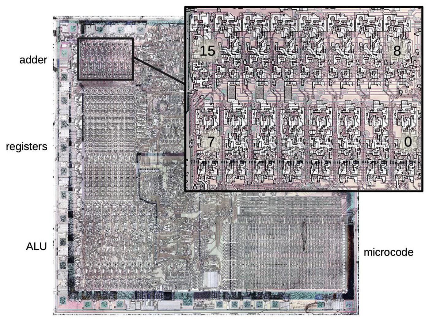
The Intel 8086 processor contains many interesting components that can be understood through reverse engineering. In this article, I'll discuss the adder that is used for address calculations. The photo below shows the tiny silicon die of the 8086 processor under a microscope. The left part of the chip has the 16-bit datapath including the registers and the Arithmetic-Logic Unit (ALU); you can see the pattern of circuitry repeated 16 times. The rectangle in the lower-right is the microcode ROM, defining the execution of each instruction.

Die photo of the 8086 microprocessor, highlighting the 16-bit address adder.  The microcode ROM is in the lower right. The metal layer has been removed for this photo, revealing the silicon and polysilicon underneath. The colors are due to thin-film effects from partially-removed oxide layers.

Die photo of the 8086 microprocessor, highlighting the 16-bit address adder. The microcode ROM is in the lower right. The metal layer has been removed for this photo, revealing the silicon and polysilicon underneath. The colors are due to thin-film effects from partially-removed oxide layers.

The 16-bit adder, the topic of this post, is in the upper left. The magnified view shows how the adder is constructed from 16 stages, one for each bit. The upper row handles the top bits (15-8) and the lower row handles the low bits (7-0).1 Studying the die reveals how this 16-bit adder was optimized through clever circuit design, specialized logic gates, and careful layout techniques.

How the adder is used in the 8086

You might wonder why the 8086 contains both an adder and an ALU (arithmetic-logic unit). The reason is that the adder is used for address calculations, while the ALU is used for data calculations. The 8086 prefetches instructions using a "Bus Interface Unit", which runs semi-independently from the "Execution Unit" that executed instructions. It would have been difficult for the Bus Interface Unit and the Execution Unit to share the ALU without conflicts. By providing both an adder2 and the ALU, the two calculations can take place in parallel.

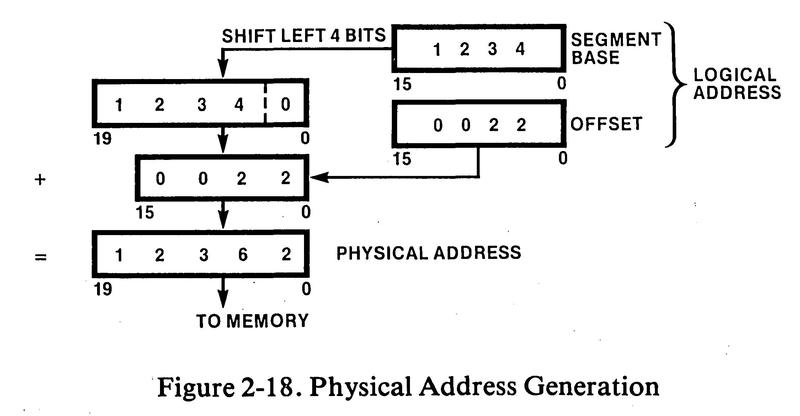
Microprocessors of the early 1970s typically had 16-bit addresses, capable of accessing 64 kilobytes of memory. At first, 64 kilobytes seemed like more memory than anyone would need (or afford), but as the price of memory chips plunged, the demand for memory grew.4 To support a larger address space, Intel added segment registers to the 8086, a hack that allowed the processor to access a megabyte of memory but led to years of gnashed teeth. The concept is to break memory into 64-kilobyte segments. A segment register specifies the start of the memory segment, and a 16-bit address indicates an address within that segment. These are combined in the adder, as shown below, to obtain the memory address. One downside is that accessing regions of memory larger than 64 kilobytes is difficult; the segment register must be modified to get outside the current segment.3

The segment register and the offset are added to create a 20-bit physical address.
From iAPX 86,88 User's Manual, page 2-13.

The segment register and the offset are added to create a 20-bit physical address. From iAPX 86,88 User's Manual, page 2-13.

How does the 16-bit adder compute a 20-bit address? The trick is that since the segment register is shifted 4 bits, the adder sums the 16 bits of the segment register and the top 12 bits of the offset. The four low bits of the offset bypass the adder since they are unchanged. For other purposes (such as incrementing the instruction counter), the adder operates on unshifted 16-bit addresses. Thus, the register circuitry has logic to feed either shifted or non-shifted values to the adder.

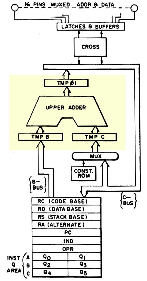
The diagram below, from the 8086 patent, shows how the adder sits between the segment registers and the address pins, computing the address. In the patent, the segment registers were named RC, RD, RS, and RA, not their current names: CS, DS, SS, and ES.

The adder, highlighted in yellow, is a key part of the Bus Interface Unit.
The upper register file (separate from the general-purpose registers) is connected to the adder.
IND and OPR are internal registers, not visible to the programmer.
From the 8086 patent.

The adder, highlighted in yellow, is a key part of the Bus Interface Unit. The upper register file (separate from the general-purpose registers) is connected to the adder. IND and OPR are internal registers, not visible to the programmer. From the 8086 patent.

The adder implementation

If you've studied digital logic, you may be familiar with the full adder, a building-block for adding binary numbers. Specifically, a full adder takes two bits and a carry-in bit. It adds these three bits and outputs the 1-bit sum, as well as a carry-out bit. (For instance 1+0+1 = 10 in binary, so the carry-out is 1 and the sum bit is 0.) A 16-bit adder can be created by joining 16 full-adders, with the carry-out from one feeding into the carry-in of the next. Just as you add two decimal numbers, moving carries to the next column on the left, each full adder adds one column in the binary numbers, and the carry is passed on to the left.

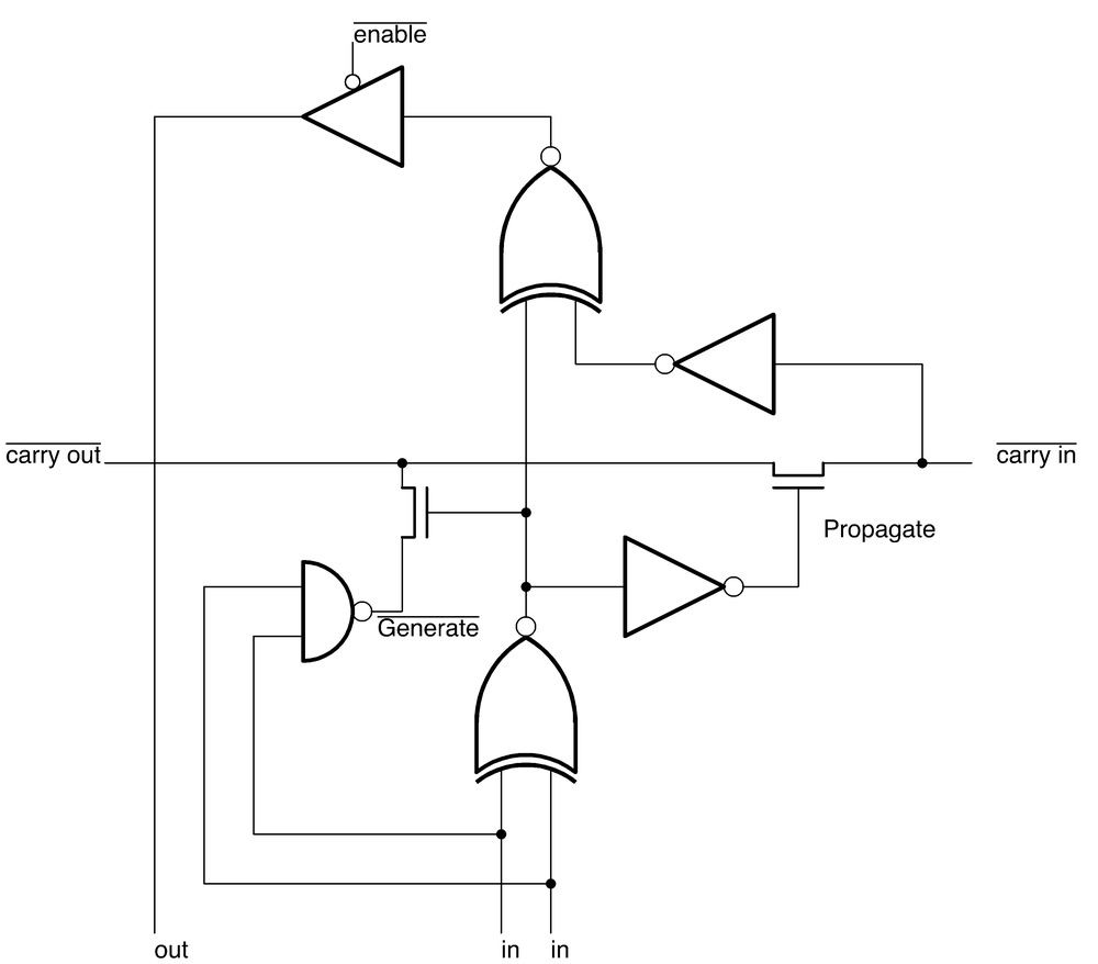
A full adder can be implemented in different ways; the 8086's circuit is shown below. (This circuit is repeated 16 times in the 16-bit adder.) Each adder stage takes two inputs (at the bottom) and the carry-in (inverted, at the right). These are summed to form a 1-bit sum output (bottom) and a carry-out (at the left). The sum bit is formed by the two exclusive-NOR gates that combine the two inputs and the carry-in.5 The output passes through a tri-state buffer (at the top), allowing it to be connected to an internal data bus.6

Schematic of one stage of the 8086's adder. The schematic layout corresponds to the physical layout on the chip.

Schematic of one stage of the 8086's adder. The schematic layout corresponds to the physical layout on the chip.

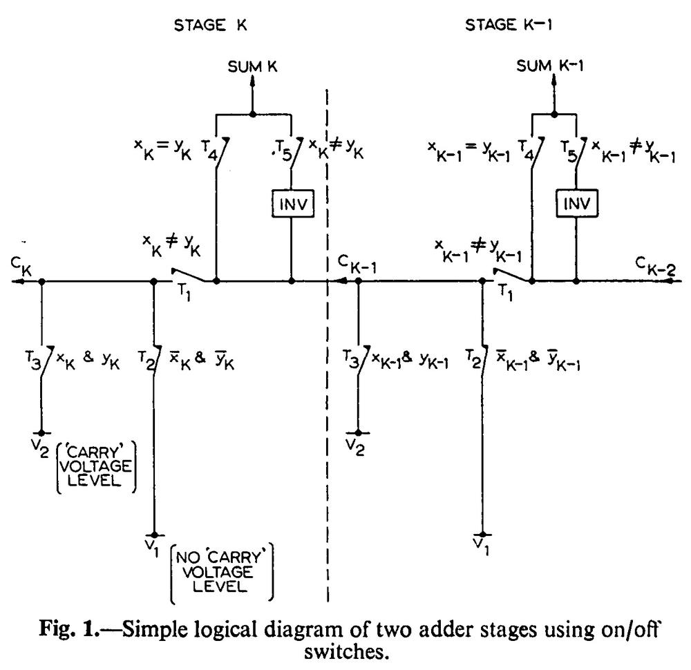
The carry computation uses an optimization called the Manchester carry chain7, dating back to 1959. The problem with addition is carries are slow; in the straightforward approach, each bit sum can't be computed until the carry to the right has been computed. (Similar to computing 99999999+1 with long addition; each digit requires you to carry the one.) If each bit must wait for the previous carry, addition becomes a slow, serial process.

The idea behind the Manchester carry chain is to decide, in parallel, if each stage will generate a carry, propagate an existing carry, or block any carry. Then, the carry can rapidly flow through the "carry chain" without sequential evaluation. To understand this, consider the cases when adding two bits and a carry-in. For 0+0, there will be no carry, regardless of any carry-in. On the other hand, adding 1+1 will always produce a carry, regardless of any carry-in; this case is called "carry generate". The interesting cases are 0+1 and 1+0; there will be a carry-out if there was a carry-in. This case is called "carry propagate" since the carry-in propagates through the stage unchanged.

The "carry generate" and "carry propagate" signals are used to open or close switches (i.e. transistors) in the carry line. For "carry propagate", carry-in is connected to carry-out, so the carry can flow through. Otherwise, the incoming carry is disconnected. For "carry generate", a carry signal is sent to carry-out. Since these switches can all be set in parallel, carry computation is quick. There is still some propagation delay as the carry-in flows through the switches, potentially from bit 0 all the way to bit 15, but this is much faster than computing the carry through a sequence of logic gates.

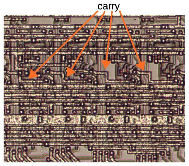
Four stages of the adder, with the carry chain indicated. In this photo, the metal layer on top of the chip is visible, mostly obscuring the polysilicon and silicon underneath. The input and output wiring for each stage is at the bottom.

Four stages of the adder, with the carry chain indicated. In this photo, the metal layer on top of the chip is visible, mostly obscuring the polysilicon and silicon underneath. The input and output wiring for each stage is at the bottom.

The carry chain is visible on the die; the photo above shows four stages of the adder. The horizontal lines are the metal wiring: control signals, ground, and power (the thick line near the bottom). The silicon circuitry is barely visible underneath the metal. The carry chain wires are interrupted at each stage, to connect to the transistors underneath, and the new carry continues on to the next stage.

Carry-skip

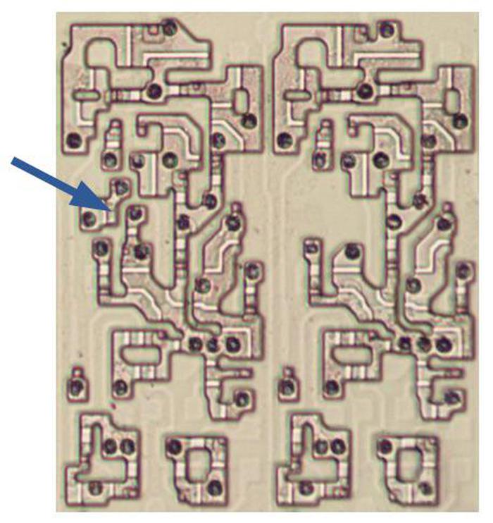
Careful examination of the adder shows that while the 16 single-bit stages are very similar, they are not all identical. The extra circuitry indicated below turns out to be a performance optimization called the carry-skip adder.

These two stages of the 8086's adder are almost identical, except for the circuitry indicated by the arrow. In this photo, the metal and polysilicon layers were removed, showing the underlying silicon.

These two stages of the 8086's adder are almost identical, except for the circuitry indicated by the arrow. In this photo, the metal and polysilicon layers were removed, showing the underlying silicon.

The idea of carry-skip is to skip over some of the stages in the carry chain if possible, reducing the worst-case delay through the chain. For example, if there is a carry-in to bit 8, and the carry propagate is set for bits 8, 9, 10, and 11, then it can be immediately determined that there is a carry-in to bit 12. Thus, by ANDing together the carry-in and the four carry-propagate values, the carry-in to bit 12 can be calculated immediately for this case. In other words, the carry skips from bit 8 to bit 12. Likewise, similar carry-skip circuits allow the carry to skip from bit 2 to bit 4, and bit 4 to bit 8. These carry-skip circuits reduced the adder's worst-case computation time.8

Regular logic vs dynamic logic

The performance of the adder is critical to the overall speed of the 8086, so it uses some interesting techniques to implement fast logic gates. Some of the adder's gates are built with dynamic logic. A standard logic gate is straightforward: you put signals in and you get the result out. In contrast, a dynamic logic gate uses a periodic clock signal to compute the logic function.9 Since dynamic logic can be faster and more compact, it is used in modern processors, in the form of domino logic.

Dynamic logic depends on a two-phase clock, commonly used for timing in microprocessors of that era. The two-phase clock consists of two clock signals that are active in alternation. First, phase 1 (ɸ1) is high and phase 2 (ɸ2) is low. Then phase 1 is low and phase 2 is high. This cycle repeats at the clock frequency, such as 5 MHz.

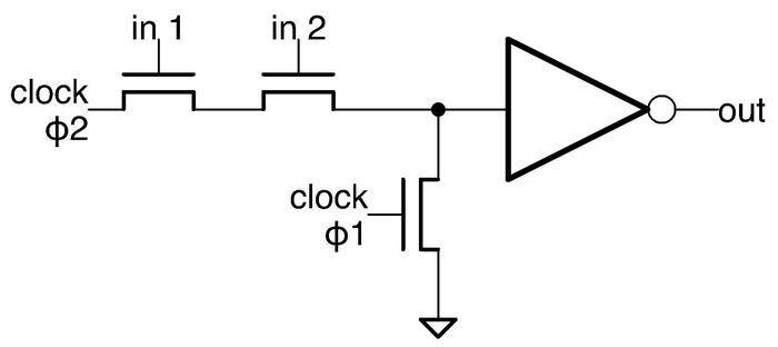
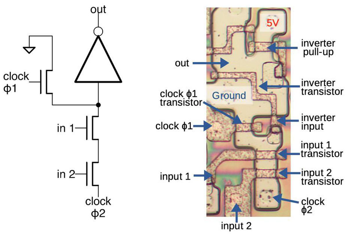
The schematic below shows a dynamic NAND gate from the adder. In phase 1, the clock ɸ1 turns on the lower transistor, pulling the input to the inverter low. Phase 2 is the evaluation phase, where the logic function is computed. If both inputs are high, the two input transistors will turn on, allowing clock ɸ2 to pass through to the inverter input, pulling it high and causing the output to be low. On the other hand, if either input is low, the clock ɸ2 cannot pass through the transistors. Instead, the inverter input remains low from the previous phase, due to the stray capacitance of the wire, so the output is high. Thus, in either case, the circuit implements the NAND functionality, with a low output only if the inputs are both high. Note that unlike a standard logic gate, the dynamic logic gate's output is only valid during clock phase 2.

Implementation of a NAND gate using dynamic logic. The gate is controlled by the two-phase clock signals.

Implementation of a NAND gate using dynamic logic. The gate is controlled by the two-phase clock signals.

The diagram below shows how the dynamic NAND gate is physically implemented on the die; the layout of the schematic corresponds to the physical layout. In the photo, the metal layer has been removed, showing the silicon underneath. The yellowish regions are doped, conductive silicon. The brownish, metallic lines are polysilicon, a special type of silicon used as wiring. A transistor is formed when polysilicon crosses doped silicon; the polysilicon is the gate, controlling conduction between the silicon on either side. The transistors have complex, twisted shapes to fit the circuitry in as little space as possible. Each transistor was given a particular size for the best balance between speed and power consumption. For example, the input transistors are small, while the inverter transistor is much larger.

A dynamic NAND gate in the 8086, with corresponding schematic. The metal layer has been removed for this photo, revealing the silicon and polysilicon.
The layout is slightly different between the lower stages (shown) and the upper stages.

A dynamic NAND gate in the 8086, with corresponding schematic. The metal layer has been removed for this photo, revealing the silicon and polysilicon. The layout is slightly different between the lower stages (shown) and the upper stages.

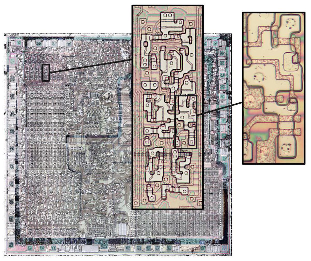
The diagram below shows the location of a NAND gate in the 8086 chip. The first box zooms in on one of the 16 single-bit adder circuits. The second box shows the position of the NAND gate within the adder. The NAND gate is almost visible in the overall die photo showing how large the features are, compared to a modern chip.

Each stage of the adder has a dynamic NAND gate. The NAND gate in one of these stages is highlighted.

Each stage of the adder has a dynamic NAND gate. The NAND gate in one of these stages is highlighted.

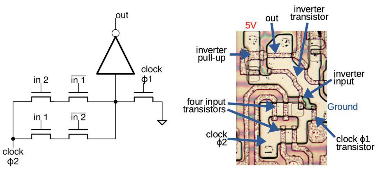
Another interesting dynamic logic gate in the adder is exclusive-NOR (XNOR, the complement of XOR), which outputs 1 if both inputs are the same, and 0 otherwise. The schematic below shows the implementation of XNOR.10 As before, during phase 1, the inverter input is pulled to ground. In the evaluation phase, clock ɸ2 can pull the inverter input high through either the upper pair of transistors or the lower pair of transistors. This will happen if the inputs are different (input 2 is high and input 1 is low, or if input 1 is high and input 2 is low), causing the inverter output to be low. Otherwise, the inverter input will remain low from phase 1, and the inverter output will be high. Thus, the output is high if the two inputs are equal, and low otherwise, the desired XNOR behavior.

A dynamic XNOR gate, as implemented on the 8086.

A dynamic XNOR gate, as implemented on the 8086.

Conclusions

The adder in the 8086 has a critical role, computing addresses for every memory access. A 16-bit adder may seem like a straightforward circuit, but the adder in the 8086 was highly optimized so it wouldn't be a performance bottleneck. To speed up carry processing, the adder uses a Manchester carry chain, with carry-skip circuitry on top of that. The adder uses three different designs for logic gates: standard NMOS gates, pass-transistor logic, and dynamic logic. Even at the transistor level, the circuit is highly optimized, with transistors of all shapes and sizes carefully packed together.

The Intel 8086 is an interesting processor with complex circuits but still simple enough that its circuits can be studied under a microscope. The 8086 has 29,000 transistors and features that are a few micrometers large. In comparison, modern processors have billions of transistors and transistors that are measured in nanometers. While the progress of Moore's law has yielded great improvements in modern processors, the processors of the 1970s are much better for reverse engineering.

If you're interested in the 8086, I wrote about the 8086 die, its die shrink process and the 8086 registers earlier. I plan to write more about the 8086 so follow me on Twitter @kenshirriff or RSS for updates.

Notes and references

  1. The adder's layout has bits 15-8 in the top and bits 7-0 below. This layout is a consequence of the bit ordering in the data path: the bits are interleaved 15-7-14-6-...-8-0, instead of linearly 15-14-...-0. The reason behind this interleaving is that it makes it easy to swap the two bytes in the 16-bit word, by swapping pairs of bits. The adder is split into two rows so it fits into the horizontal space available. Even with the tall, narrow layout of an adder stage, a bit of the adder is wider than a bit of the register file. Splitting the adder into two rows keeps the bit spacing approximately the same, avoiding long wires between the register file and the adder. 

  2. Many early microprocessors (such as the 6502 and Z-80) had an incrementer for the program counter, separate from the ALU. (One motivation was the ALU was 8 bits while the program counter was 16 bits.) The 68000 had address adders, separate from the ALU. 

  3. The 8086's segmented architecture led to programming with near pointers and far pointers. A near pointer was a 16-bit pointer that could be held in a register and manipulated easily, but couldn't access more than 64 kilobytes. A far pointer was the combination of an offset and a segment value, resulting in a pointer that could access the full memory but required twice the storage for each pointer. Comparing far pointers was problematic, since they were not unique; multiple offset/segment combinations could address the same physical memory address. 

  4. In contrast to the 8086, the Motorola 68000 microprocessor (1979) had 32-bit registers. Its address bus was 24 bits wide, allowing it to access 16 megabytes of memory directly, without segment registers. The 68020 (1984) extended the address bus to 32 bits, allowing 4 gigabytes of memory to be accessed.

    The 68000 was provided in a 64-pin package, providing plenty of pins for the 24 address lines and 16 data lines. In comparison, Intel didn't like large IC packages and used a 40-pin package for the 8086. As a result, the 8086 used 20 pins for the address lines, and reused (i.e. multiplexed) 16 of these pins for data lines. The 8086 also multiplexed many of the control pins, complicating system design. 

  5. The desired sum output is input1⊕input2⊕carry-in. In the 8086 adder, the carry-in is inverted, there are two exclusive-NOR gates, and an inverter in the path. Thus, the circuit has four inversions in total; since this number is even, they cancel out and the circuit produces the desired exclusive-OR of the three values. 

  6. A tri-state buffer has three different outputs: high (1), low (0), or high-impedance (hi-Z). In the hi-Z state, the buffer is not outputting anything and is electrically disconnected. The motivation for this is that multiple signals can be connected to a bus through tri-state buffers. By enabling one buffer and disabling the rest, the desired signal can be output to the bus. (Regular buffers wouldn't work because electrical problems would arise if one buffer outputs a 1 and another outputs a 0.) Open-collector outputs are an alternative for connecting multiple signals to a bus. 

  7. The Manchester carry chain was developed by the University of Manchester and described in the article Parallel addition in digital computers: a new fast 'carry' circuit, 1959. It was used in the Atlas supercomputer (1962).

    The original diagram showing how the Manchester carry chain is implemented, from 1959.

    The original diagram showing how the Manchester carry chain is implemented, from 1959.

    The diagram above, from the original article, shows the structure of the Manchester carry chain. Although the switches look like relay contacts, the carry chain was implemented with transistors (2N501 micro-alloy diffused-base transistors). The structure of the carry chain in the 8086 is similar to the diagram above, but the top switches are replaced by XNOR gates. 

  8. A few notes on the carry-skip implementation. Conceptually the signals are ANDed together, but the implementation uses a NOR gate since the carry and propagate signal inputs are inverted. For carry-skip to be useful, computing the carry with a gate must be faster than the carry chain, which was achieved by skipping four stages at a time. (I don't know why the first stage was implemented with a smaller skip.) Note that carry-skip helps in specific cases (which include the worst-case), so the regular carry circuitry is still required. 

  9. Processors always have a maximum clock speed, the fastest they can run. (The original 8086 ran at up to 5 MHz, while the later 8086-1 supported 10 MHz.) However, due to the use of dynamic logic, the 8086 also had a minimum clock speed of 2 MHz. If the clock ran slower than that, there was a risk of the charge on a wire leaking away before it was used, causing errors. 

  10. Surprisingly, the adder uses a completely different implementation for the upper XNOR gate; it is implemented with pass-transistor logic rather than dynamic logic. I think the motivation is that the carry-in signal to these XNOR gates is not quite synchronous, due to propagation delay through the carry chain. Dynamic logic has the disadvantage that if an input signal switches low after the clock, the gate can't recover; the circuit has been charged and won't be discharged until the next clock phase. In particular, if a carry comes in after clock phase 2 has started, it can't switch the output high. By using non-dynamic logic, the output will switch correctly when the carry arrives, even if it is not aligned with the clock.

    Pass-transistor logic is different from "regular" NMOS logic gates, but provides a more efficient way of implementing XNOR. The circuit is similar to the XNOR in the Z-80 microprocessor, which I've described earlier, so I won't go into more detail here.

    Pass-transistor logic is also used to implement the input and output latches on the adder. On the patent diagram shown earlier, these latches appear as "TMP B" and "TMP C" on the input side of the adder and "TMP ɸ1" on the output side. These latches are necessary because otherwise the adder's output would be connected directly to the input, causing the adder to repeatedly add. The implementation of these latches is simply clocked pass transistors in the path, holding the value by capacitance. 

Inside the 8086 processor, tiny charge pumps create a negative voltage

Introduced in 1978, the revolutionary Intel 8086 microprocessor led to the x86 processors used in most desktop and server computing today. This chip is built from digital circuits, as you would expect. However, it also has analog circuits: charge pumps that turn the 8086's 5-volt supply into a negative voltage to improve performance.1 I've been reverse-engineering the 8086 from die photos, and in this post I discuss the construction of these charge pumps and how they work.

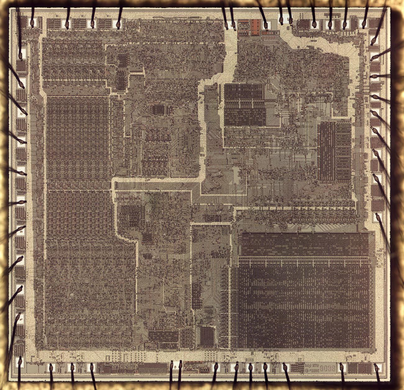
Die photo of the 8086 microprocessor. The ALU and registers are on the left. The microcode ROM is in the lower right. Click for a high-resolution image.

Die photo of the 8086 microprocessor. The ALU and registers are on the left. The microcode ROM is in the lower right. Click for a high-resolution image.

The photo above shows the tiny silicon die of the 8086 processor under a microscope. The metal layer on top of the chip is visible, with the silicon hidden underneath. Around the outside edge, bond wires connect pads on the die to the chip's 40 external pins. However, careful examination shows that the die has 42 bond pads, not 40. Why are there two extra ones?

An integrated circuit starts with a silicon substrate, and transistors are built on this. For high-performance integrated circuits, it is beneficial to apply a negative "bias" voltage to the substrate. 2 To obtain this substrate bias voltage, many chips in the 1970s had an external pin that was connected to -5V,3 but this additional power supply was inconvenient for the engineers using these chips. By the end of the 1970s, however, on-chip "charge pump" circuits were designed that generated the negative voltage internally. These chips used a single convenient +5V supply, making engineers happier.

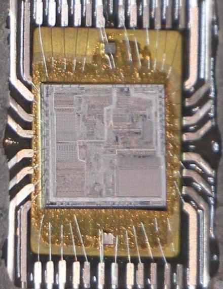
A closeup of the 8086 chip showing the silicon die and the bond wires connecting it to the lead frame.

A closeup of the 8086 chip showing the silicon die and the bond wires connecting it to the lead frame.

On the 8086 die, the two extra pads feed this negative bias voltage to the substrate. The photo above shows the silicon die as mounted in the chip, with bond wires connected to the lead frame that forms the pins. Looking carefully, there are two small gray squares above and below the die; each connected to one of the "extra" bond pads. The charge pumps on the 8086 die generate a negative voltage, which passes through the bond wires to these squares, and then through the metal plate underneath to the 8086's substrate.

How the charge pumps work

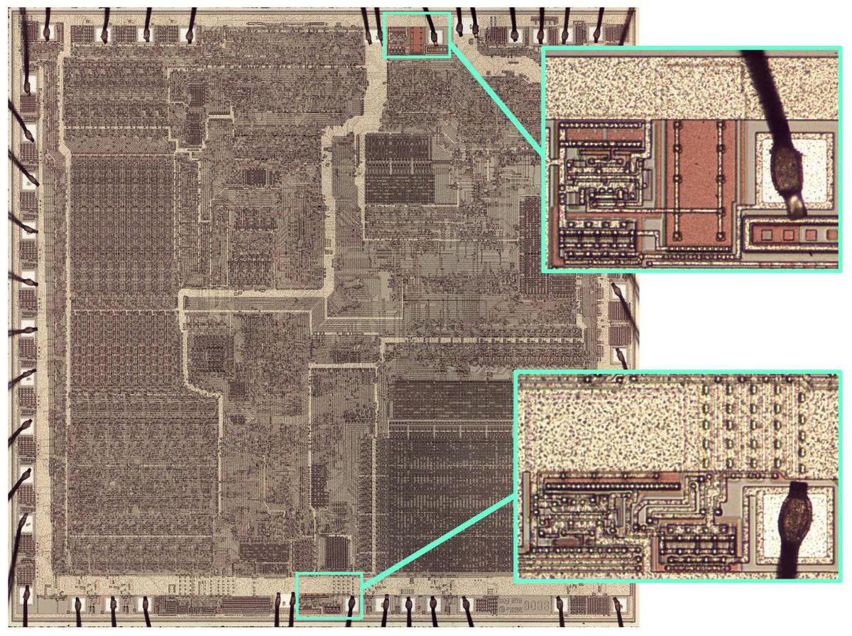
The photo below highlights the two charge pumps in the 8086. I'll discuss the top one; the bottom one has the same circuitry but a different layout to fit in the available space. Each pump has driver circuitry, a large capacitor, and a pad with the bond wire to the substrate. Each pump is located next to one of the 8086's two ground pads, presumably to minimize electrical noise.

Die photo of the 8086 microprocessor, zooming in on the two substrate bias generators.

Die photo of the 8086 microprocessor, zooming in on the two substrate bias generators.

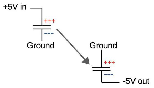
You might wonder how a charge pump can turn a positive voltage into a negative voltage. The trick is a "flying" capacitor, as shown below. On the left, the capacitor is charged to 5 volts. Now, disconnect the capacitor and connect the positive side to ground. The capacitor still has its 5-volt charge, so now the low side must be at -5 volts. By rapidly switching the capacitor between the two states, the charge pump produces a negative voltage.

On the left, the "flying capacitor' is charged to 5 volts. By switching ground to the upper terminal, the capacitor now outputs -5 volts. (source)

On the left, the "flying capacitor' is charged to 5 volts. By switching ground to the upper terminal, the capacitor now outputs -5 volts. (source)

The 8086's charge pump circuit uses MOSFET transistors and diodes to switch the capacitor between the two states, with an oscillator to control the transistors, as shown in the schematic below. The ring oscillator consists of three inverters connected in a loop (or ring). Because the number of inverters is odd, the system is unstable and will oscillate.5 For instance, if the input to the first inverter is 0, its output will be 1, the second output will be 0, and the third output will be 1. This will flip the first inverter, and the "flip" will travel through the loop causing oscillation. To slow down the oscillation rate, two resistor-capacitor networks are inserted into the ring. Since the capacitors will take some time to charge and discharge, the oscillations will be slowed, giving the charge pump time to operate.4

Schematic of the charge pump used in the Intel 8086 to provide negative substrate bias.

Schematic of the charge pump used in the Intel 8086 to provide negative substrate bias.

The outputs from the ring oscillator are fed to the transistors that drive the capacitor. In the first step, the upper transistor is switched on, causing the capacitor to charge through the first diode to 5 volts with respect to ground. The second step is where the magic happens. The lower transistor turns on, connecting the high side of the capacitor to ground. Since the capacitor is still charged to 5 volts, the low side of the capacitor must now be at -5 volts, producing the desired negative voltage. This goes through the second diode and the bond wire to the substrate. When the oscillator flips again, the upper transistor turns on and the cycle repeats. The charge pump gets its name because it pumps charge from the output to ground.6 The diodes are similar to check valves in a water pump, making sure charge moves in the right direction.

The implementation in silicon

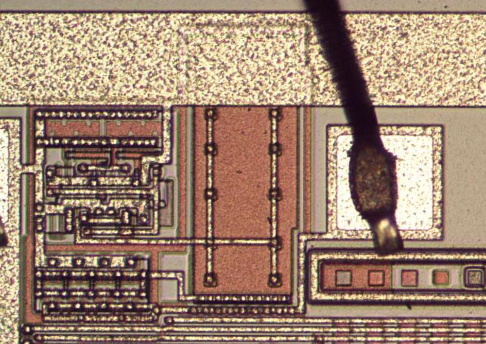
The photo below shows the charge pump as it is implemented on the chip. In this photo, the metal wiring is visible on top, with reddish polysilicon underneath and beige silicon at the bottom. The main capacitor is visible in the center, with H-shaped wiring connecting it to the circuitry on the left. (Part of the capacitor is hidden under the wide metal power trace at the top.) On the right, the substrate bond wire is attached to the pad. A test pattern is below the pad; it has a square for each mask used to produce a layer of the chip.

The charge pump, showing the metal layer.

The charge pump, showing the metal layer.

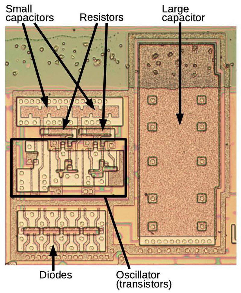
Removing the metal layer shows the circuitry more clearly, below. The large charge pump capacitor takes up the right half of the photo. Although microscopic, this capacitor is huge by chip standards, about the size of a 16-bit register. The capacitor consists of polysilicon over a silicon region, separated by insulating oxide; the polysilicon and silicon form the plates of the capacitor. On the left side are the smaller capacitors and the resistors that provide the R-C delay for the oscillator. Below them is the oscillator circuitry and the drive transistors.7

An 8086 charge pump, showing the key components. The metal has been removed for this photo, to show the silicon and polysilicon underneath.

An 8086 charge pump, showing the key components. The metal has been removed for this photo, to show the silicon and polysilicon underneath.

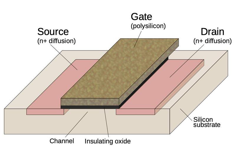
One interesting feature of the charge pump is the two diodes, each built from eight transistors in a regular pattern. The diagram below shows the structure of a transistor. Regions of the silicon are doped with impurities to create diffusion regions with desired properties. The transistor can be viewed as a switch, allowing current to flow between two diffusion regions called the source and drain. The transistor is controlled by the gate, made of a special type of silicon called polysilicon. A high voltage on the gate lets current flow between the source and drain, while a low voltage blocks current flow. These tiny transistors can be combined to form logic gates, the components of microprocessors and other digital chips. But in this case, the transistors are used as diodes.

Structure of an NMOS transistor (MOSFET) as implemented in an integrated circuit.

Structure of an NMOS transistor (MOSFET) as implemented in an integrated circuit.

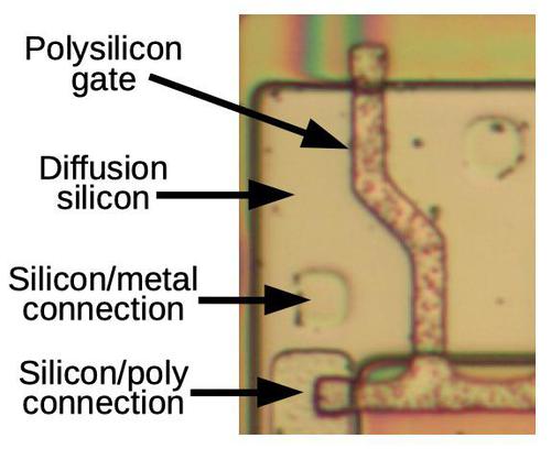
The photo below shows a transistor in the charge pump, viewed from above. As in the diagram, polysilicon forms the gate between the silicon diffusion regions on either side. A diode can be formed from a MOSFET by connecting the gate and drain together (details) through the silicon/polysilicon connection at the bottom of the photo. The silicon can also be connected to the metal layer through a "via". The metal layer was removed for this photo, but faint circles indicate the position of silicon/metal vias.

A transistor in the charge pump circuit. The polysilicon gate separates the transistor's source and drain on either side.

A transistor in the charge pump circuit. The polysilicon gate separates the transistor's source and drain on either side.

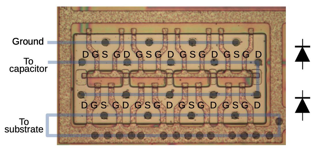
The diagram below shows how the two diodes are implemented from 16 transistors. To support the relatively high current of the charge pump, eight transistors are used in parallel for each diode. Note that neighboring transistors share source or drain regions, allowing transistors to be packed densely. The blue lines indicate the metal wires; the metal was removed for this photo. The dark circles indicate connections (vias) between the metal and silicon.

The charge pump has two diodes, each implemented with 8 transistors. The source, gate, and drain are indicated with S, G, and D.

The charge pump has two diodes, each implemented with 8 transistors. The source, gate, and drain are indicated with S, G, and D.

Putting this all together, the upper eight transistors have their sources connected to ground by a metal wire. Their gates and drains connected together by the polysilicon below the transistors, making them into diodes, and they are connected to the capacitor by a metal wire. The lower eight transistors form a second diode; their gates and drains are wired together by the lower metal wire loop. Note how the layout has been optimized; for example, the gates have bent shapes to avoid the vias (black dots).

Conclusions

The substrate bias generator on the 8086 chip9 is an interesting combination of digital circuitry (a ring oscillator formed from inverters) and an analog charge pump. While the bias generator may seem like an obscure part of 1970s computer history, bias generation is still part of modern integrated circuits. It is much more complex in modern chips which have multiple carefully regulated biases in multiple power domains. 8 In a sense it is analogous to the x86 architecture, something that started in the 1970s and is even more popular today, but has become unimaginably more complex in the quest for higher performance.

If you're interested in the 8086, I wrote about the 8086 die, its die shrink process and the 8086 registers earlier. I plan to analyze the 8086 in more detail in future blog posts so follow me on Twitter @kenshirriff or RSS for updates.

Notes and references

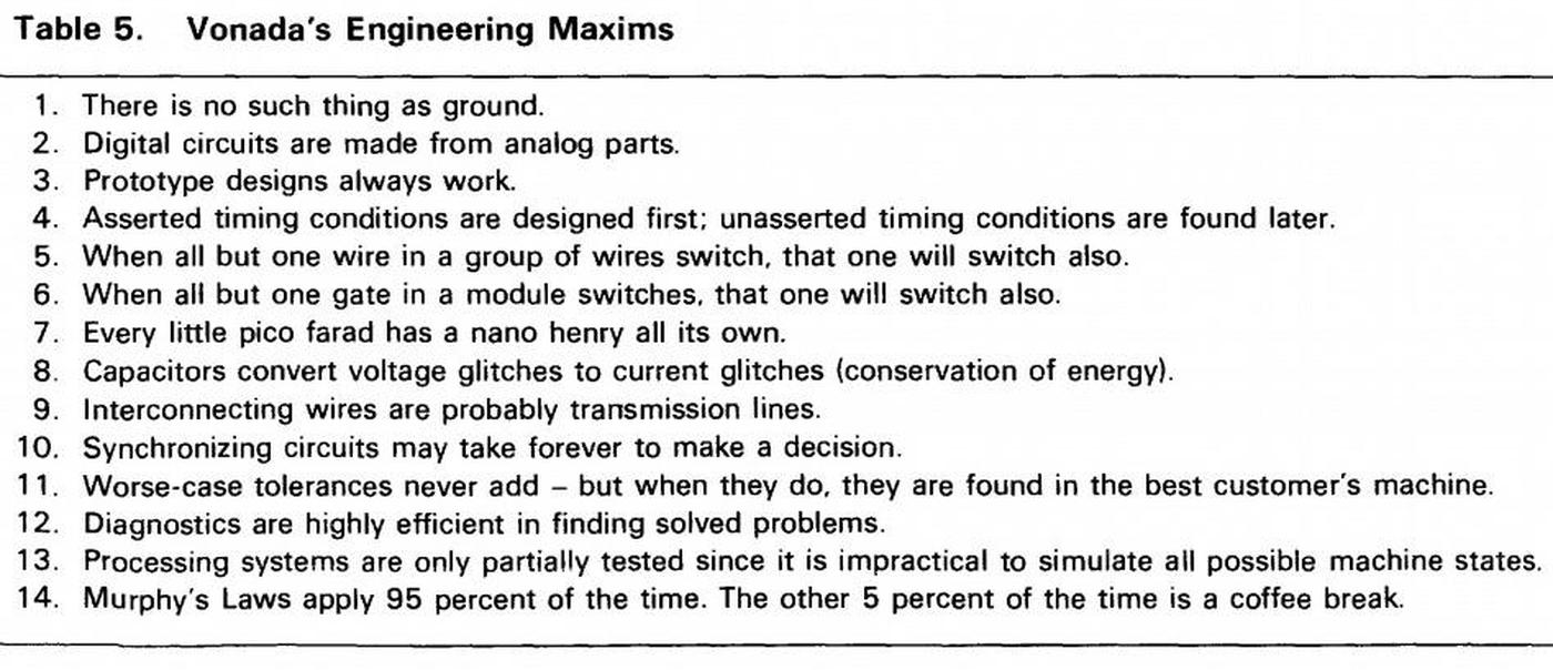
  1. Strictly speaking, the entire chip is analog: there's an old saying that "Digital computers are made from analog parts". This saying came from DEC engineer Don Vonada and was published in DEC's Computer Engineering in 1978.

    Vonada's Engineering Maxims (text).

    Vonada's Engineering Maxims (text).


  2. Putting a negative bias voltage on the substrate had several benefits. It decreased parasitic capacitance making the chip faster, made the transistor threshold voltage more predictable, and reduced leakage current

  3. Early DRAM memory chips and microprocessor chips often required three supplies: +5V (Vcc), +12V (Vdd) and -5V (Vbb) bias voltage. In the late 1970s, improvements in chip technology allowed a single supply to be used instead. For example, Mostek's MK4116 (a 16 kilobit DRAM from 1977) required three voltages while the improved MK4516 (1981) operated on a single +5V supply, simplifying hardware designs. (Amusingly, some of these chips still kept the Vbb and Vcc pins for backward compatibility but left them unconnected.) Intel's memory chips followed a similar path, with the 2116 DRAM (16K, 1977) using three voltages and the improved 2118 (1979) using a single voltage. Similarly, the famous Intel 8080 microprocessor (1974) used enhancement-mode transistors and required three voltages. An improved version, the 8085 (1976), used depletion-mode transistors and was powered by a single +5V supply. The Motorola 6800 microprocessor (1974) used a different approach for a single supply; although the 6800 was built from the older enhancement-load transistors it avoided the +12 supply by implementing an on-chip voltage doubler, a charge pump that increased the voltage. 

  4. I tried to measure the frequency of the charge pump by looking at the chip's current to see fluctuations due to the charge pump. I measured 90 MHz fluctuations, but I suspect I was measuring noise and not the charge pump's oscillations. 

  5. Because the circuit has an odd number of inverters, it oscillates. If, on the other hand, it had an even number of inverters, it would be stable in two different states. This technique is used in the 8086's registers: a pair of inverters stores each bit (details). 

  6. I've simplified the charge pump discussion slightly. Due to voltage drops in the transistors, the substrate voltage will probably be around -3V, not -5V. (If a chip requires a larger voltage drop, charge pump stages can be cascaded.) For the pump direction, I'm referring to current flow. If you think of it as pumping electrons, the negative electrons are being pumped the opposite direction, into the substrate. 

  7. The oscillator is built from 13 transistors. Seven transistors form the 3 inverters (one inverter has an extra transistor to provide extra output current. The six drive transistors consist of two transistors pulling the output high and four transistors pulling the output low. The layout is strangely different from normal inverter circuitry, probably because the current requirements are different from normal digital logic. 

  8. Bias generators are now available as IP blocks that can be licensed and be plugged into a chip design. For more information on bias in modern chips, see Body bias, Multi bias domain implementation, or this presentation. There is even a standard IEEE 1801 power format that allows IC design tools to generate the necessary circuitry. 

  9. The Intel 8087, the math coprocessor chip that goes along with the 8086, also has a substrate bias generator. It uses the same principles, but unexpectedly has a different circuit, using 5 inverters. I wrote about it in detail here