The Intel 8086 processor's registers: from chip to transistors

The Intel 8086 microprocessor is one of the most influential chips ever created; it led to the x86 architecture that dominates desktop and server computing today. I've been reverse-engineering the 8086 from die photos, and in this post I discuss how its register file is implemented.

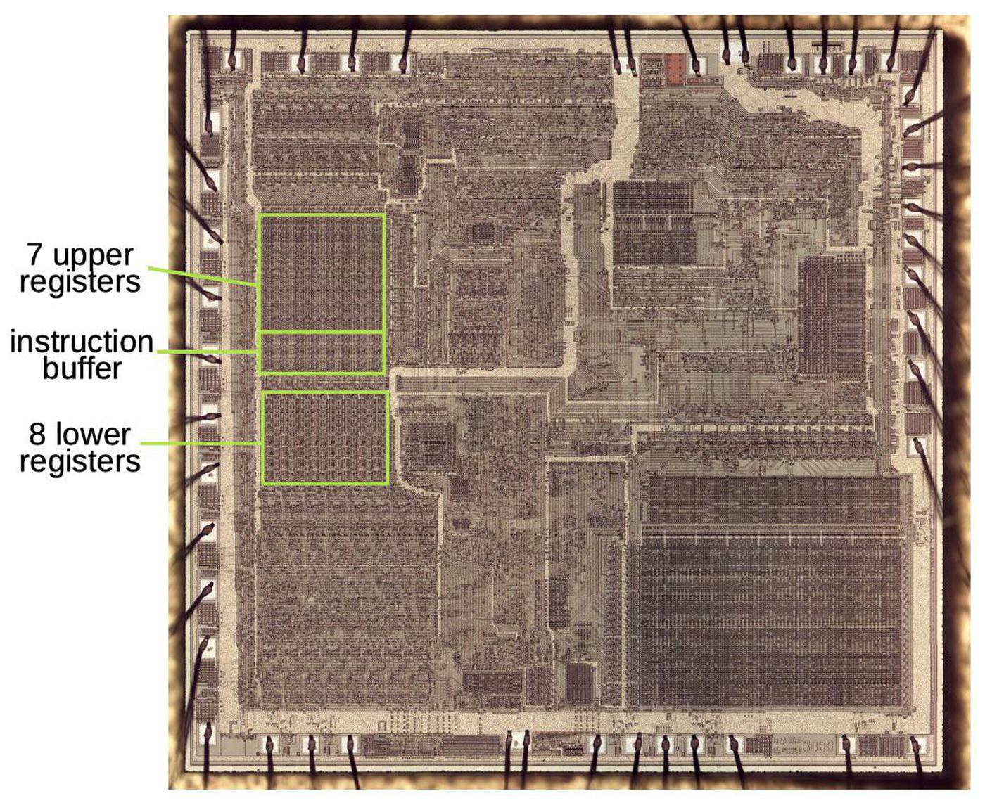
The 8086 die, showing the register storage. The upper registers are used by the Bus Interface Unit for memory accesses,
while the general-purpose lower registers are used by the Execution Unit. The instruction buffer is a 6-byte queue of prefetched
instructions.

The 8086 die, showing the register storage. The upper registers are used by the Bus Interface Unit for memory accesses, while the general-purpose lower registers are used by the Execution Unit. The instruction buffer is a 6-byte queue of prefetched instructions.

The photo above shows the silicon die of the 8086 processor under a microscope. The metal layer on top of the chip is visible, with the silicon hidden underneath. Around the outside edge, bond wires connect pads on the die to the chip's 40 external pins.

The highlighted region indicates the 8086's fifteen 16-bit registers and six bytes of instruction prefetch queue.1 Registers take up a significant portion of the die, even though they are just 36 bytes in total. Due to space limitations, early microprocessors had a relatively small number of registers; in comparison, a modern processor chip has kilobytes of registers and megabytes of cache storage.2

How a register is implemented in silicon

I'll start by explaining how the 8086 is built from NMOS transistors. Then I'll explain how an inverter is constructed, how a single bit is stored using inverters, and how a register is constructed.

The 8086 and other chips of that era were built from a type of transistor called NMOS. These chips consisted of a silicon substrate, which was "doped" by diffusion of arsenic or boron to form transistors. Above the silicon, polysilicon wiring created the gates of the transistors and wired components together. Finally, a metal layer on top provided more wiring. (Modern processors, in comparison, use CMOS technology, which combines NMOS and PMOS transistors, and they have many metal layers.)

The schematic below shows an inverter built from an NMOS transistor and a resistor3 With a low input, the transistor is off, so the pull-up resistor pulls the output high. With a high input, the transistor turns on, connecting ground and the output, pulling the output low. Thus, the input signal is inverted.

This schematic shows how an inverter is created from a transistor and resistor. The photo shows the implementation on the chip.
The metal layer was removed to show the polysilicon and silicon underneath.

This schematic shows how an inverter is created from a transistor and resistor. The photo shows the implementation on the chip. The metal layer was removed to show the polysilicon and silicon underneath.

The photo above shows how an inverter is physically constructed in the 8086. The pinkish regions are conductive doped silicon and the sparkly copper-colored lines are polysilicon on top. A transistor is created where polysilicon crosses silicon: the polysilicon forms the transistor's gate, while the silicon regions on either side are the transistor's source and drain. The large polysilicon rectangle forms the pull-up resistor between +5 volts and the output. Thus, the chip's circuitry matches the inverter schematic. Under a microscope, circuits such as this inverter are visible and can be reverse-engineered.

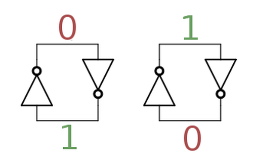
The building block for the registers is two inverters in a feedback loop, storing a single bit, as shown below. If the top wire has a 0, the right inverter will output a 1 to the bottom wire. The left inverter will then output a 0 to the top wire, completing the cycle. Thus, the circuit is stable and will "remember" the 0. Likewise, if the top wire is a 1, this will get inverted to a 0 at the bottom wire, and back to a 1 at the top. Thus, this circuit can store either a 0 or a 1, forming a 1-bit memory.

In the 8086, two coupled inverters hold a single bit in the register. This circuit is stable in either the 0 or 1 state.

In the 8086, two coupled inverters hold a single bit in the register. This circuit is stable in either the 0 or 1 state.

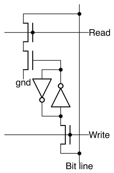
Three transistors are added to make a usable register cell from the inverter pair.4 One transistor selects the cell for reading, another transistor selects the cell for writing, and the third amplifies the signal when reading. In the center of the schematic below, two inverters store the bit. To read the bit, the read line is energized. This connects the inverter output to the bit line through the amplifying transistor. To write the bit, the write line is energized, connecting the bit line to the inverters. By putting a high-current 0 or 1 signal on the bit line, the inverters (and thus the stored bit) are forced to the desired value. Note that the bit line is used for both reading and writing.

Schematic diagram of a register cell storing a single bit. The register file is built from an array of these cells.

Schematic diagram of a register cell storing a single bit. The register file is built from an array of these cells.

The register file consists of a matrix of register cells like the one above. The matrix is 16 cells wide since registers are 16 bits wide. Each register is arranged horizontally, so a read line or write line select all the cells for a particular register. The 16 vertical bit lines form a bus, so all 16 bits in the selected register are read or written in parallel.

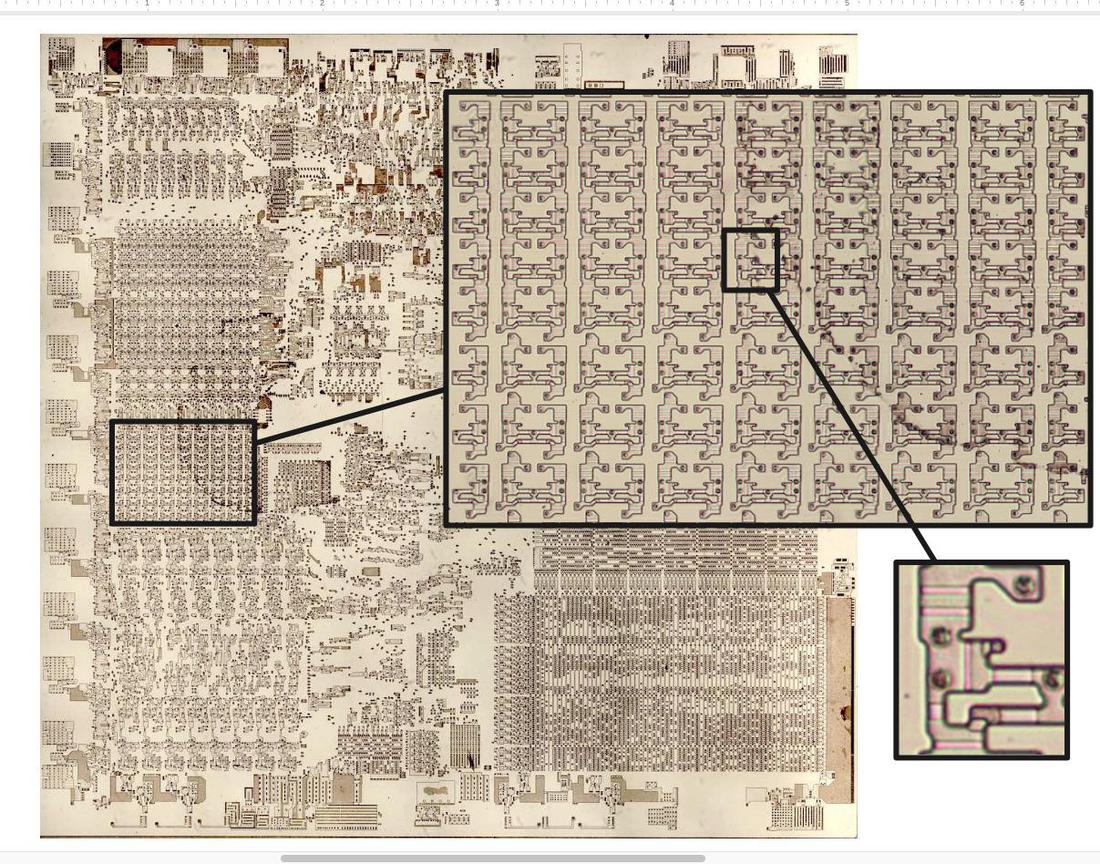
The photo below zooms in on the 8086's general-purpose register file, showing the matrix of register cells: 16 columns and 8 rows for eight 16-bit registers. It then zooms in on a single register cell in the register file. I'll now explain how this cell is implemented.

Die photo of the 8086, zooming in on the lower register file (eight 16-bit registers) and then a single register cell. The metal and polysilicon were removed for this photo to show the silicon structures.

Die photo of the 8086, zooming in on the lower register file (eight 16-bit registers) and then a single register cell. The metal and polysilicon were removed for this photo to show the silicon structures.

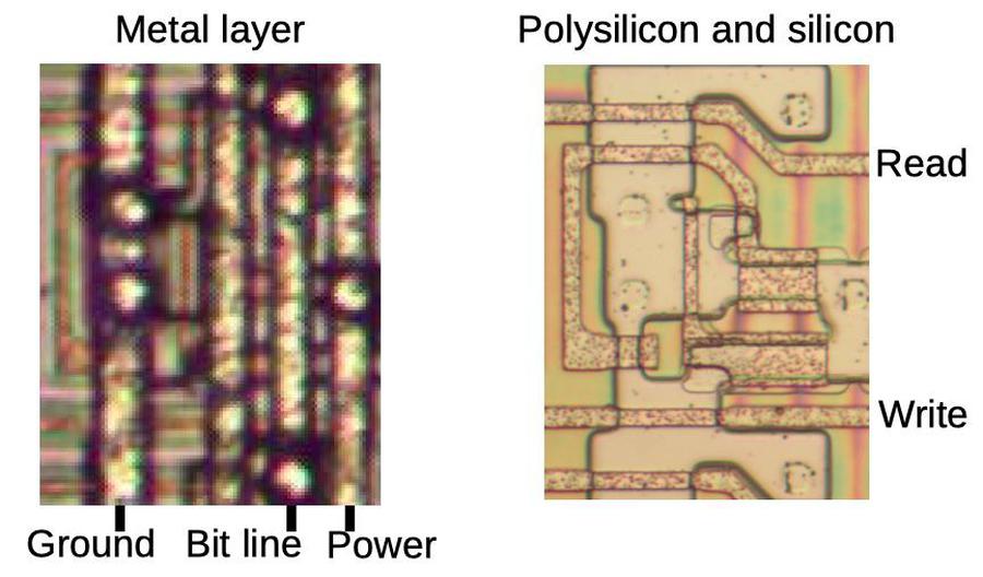
The 8086 is constructed from doped silicon and polysilicon wiring with metal wiring on top. The left photo below shows the vertical metal wiring of a register cell. The ground, power, and bit line wires are indicated. (The remaining wire crosses the register file but isn't connected to it.) In the right photo, the metal layer has been dissolved to show the polysilicon and silicon underneath. The read and write lines are horizontal polysilicon wires. (Because the chip has only one layer of metal, the register uses metal for the vertical lines and polysilicon for the horizontal lines so they don't run into each other.) The connections (called vias) between the metal and the silicon are visible as brighter circles in the metal photo and as circular spots in the silicon photo.

A register storage cell. The photo on the left shows the metal layer, while the photo on the right
shows the corresponding polysilicon and silicon underneath. The bright circles on the metal layer are vias connected to the circles on the silicon.

A register storage cell. The photo on the left shows the metal layer, while the photo on the right shows the corresponding polysilicon and silicon underneath. The bright circles on the metal layer are vias connected to the circles on the silicon.

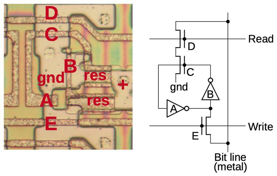
The diagram below shows how the physical layout of the register cell matches up with the schematic. The inverters are formed from transistors A and B, along with the resistors. Transistors C, D, and E are formed by the labeled strips of polysilicon. The bit line is not visible below, since it is in the metal layer. Note that the layout of the memory cell is highly optimized to minimize its size. Also note that transistor A is much smaller than the other transistors; inverter A has a weak output so it can be overpowered by the bit line when a value is written.

A register cell in the 8086 with the corresponding schematic.

A register cell in the 8086 with the corresponding schematic.

8-bit register support

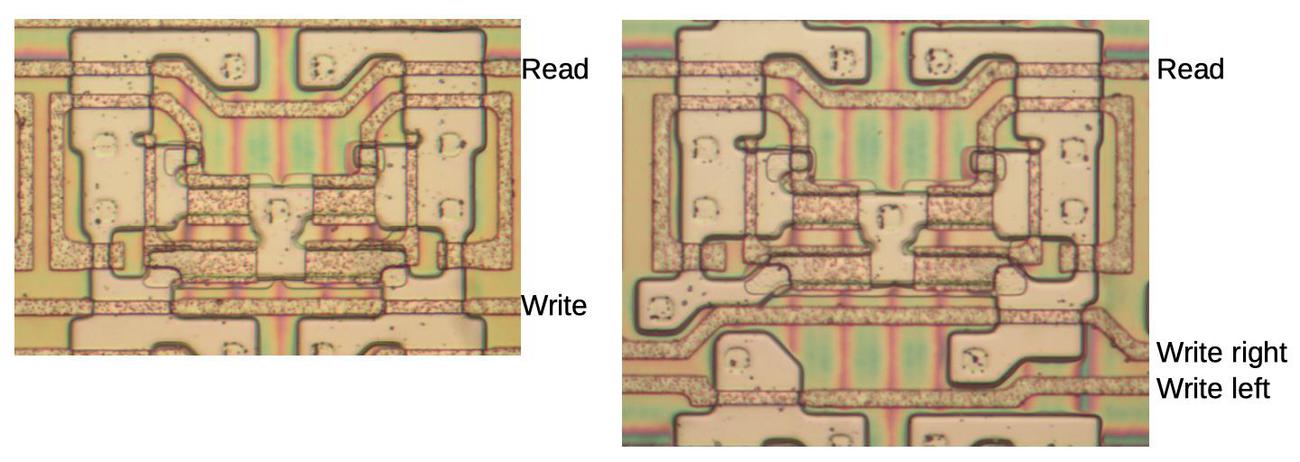
Careful examination of the die shows that some of the register cells have a slightly different structure. On the left is a pair of the register cells discussed above,5 while the right photo shows a pair of register cells with two write control lines instead of one. In the left photo, the write line crosses the silicon in both register cells. However, in the right photo, the "write right" line crosses the silicon on the right side but goes between the silicon regions on the left. Conversely, the "write left" line crosses the silicon on the left side and goes between the silicon on the right. Thus, one write line controls writes to the right-hand bit, while the other controls writes to the left-hand bit. In the full 16-bit register, this allows alternating 8-bit parts to be written separately.6

Two pairs of memory cells, showing different circuitry. The left cells have a single write line, while the right cells have separate write lines for the left and right bits.

Two pairs of memory cells, showing different circuitry. The left cells have a single write line, while the right cells have separate write lines for the left and right bits.

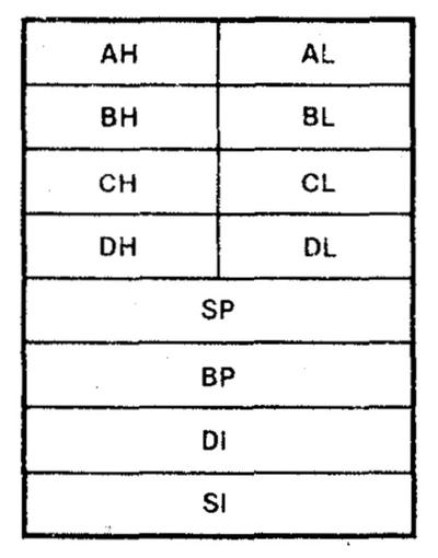
Why do some registers have two write lines while others have one? The reason is that the 8086 has 16-bit registers, but four of them can also be accessed as 8-bit registers, as shown below. For example, the 16-bit accumulator A can be accessed as an 8-bit AH (accumulator high) register and an 8-bit AL (accumulator low) register. By implementing the registers with two write control lines, either half of the register can be written separately.7

The general-purpose registers in the 8086 processor. The A, B, C, and D registers can be split into two 8-bit registers. From The 8086 Family User's Manual.

The general-purpose registers in the 8086 processor. The A, B, C, and D registers can be split into two 8-bit registers. From The 8086 Family User's Manual.

Multi-port registers

So far, I've discussed the eight general-purpose "lower registers". The 8086 also has seven "upper registers" used for memory accesses, including the infamous segment registers.8 These registers have a more complex "multi-port" design, allowing multiple reads and writes to take place simultaneously.9 For instance, the multi-ported register file would allow the program counter to be read, a segment register to be read, and a different segment register to be written, all at the same time.

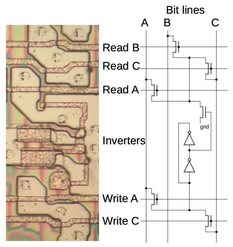
The multi-ported register cell below is built around the same two-inverter circuit as before but it has three bit lines (compared to one earlier) and five control lines (compared to two). The three read control lines allow the register cell contents to be read to any of the three bit lines, while the two write control lines allow bit line A or bit line C to be written to the register cell.

A multi-ported register cell in the 8086 processor.

A multi-ported register cell in the 8086 processor.

At first glance, the 8086's register file looked like a uniform set of registers, but close examination reveals that each register has been optimized based on its function.10 Some registers are simple 16-bit registers, which have the most compact layout. Other 16-bit registers can also be accessed as two 8-bit registers, requiring another control line. The most complex registers have two or three read ports and one or two write ports. In each case, the physical layout of the register cell has been carefully designed to be as compact as possible, with elaborate transistor shapes, as seen below. Intel's engineers shrunk the register layout as much as possible to fit all the registers in the available space.

The upper register file, consisting of ten 16-bit registers. This photo shows the silicon and polysilicon. The vertical red lines are traces of the metal layer that was removed. Click for a larger image.

The upper register file, consisting of ten 16-bit registers. This photo shows the silicon and polysilicon. The vertical red lines are traces of the metal layer that was removed. Click for a larger image.

Conclusions

Although the 8086 processor is 42 years old, it still heavily influences modern computing through the x86 architecture in heavy use today. The registers of the 8086 still exist in modern x86 computers, although the registers are now 64 bits long and have been joined by many new registers.

The 8086 is an interesting subject for die analysis since its transistors are large enough to be visible under a microscope. It was a complex processor at the time, with 29,000 transistors, but it is still simple enough that the circuitry can be traced out and understood. I plan to analyze the 8086 in more detail in future blog posts so follow me on Twitter @kenshirriff or on RSS for updates.11

Notes and references

  1. The 8086 was apparently the first microprocessor to implement instruction prefetching. The Motorola 68000 (1979) had a 4-byte instruction prefetch buffer. Prefetching in mainframes goes back to the IBM Stretch (1961), CDC 6600 (1964), and IBM System/360 Model 91 (1966). 

  2. It's difficult to determine how many registers are in a modern processor; the only accurate description I could find was in The Anatomy of a High-Performance Microprocessor, which describes the AMD K6 processor (1997) in detail. Due to register renaming modern processors have many more physical registers than architectural registers (the registers visible to a programmer), and the number of physical registers is not documented. (In addition to the eight general-purpose x86 registers, the K6 had 16 microarchitecture scratch registers for renaming.)

    Processors supporting AVX-512 include 32 512-bit registers, so that's 2 kilobytes of registers for that feature alone. This makes it even harder to determine the register size. As for cache size, high-end processors have up to 77 MB of cache storage.) 

  3. The pull-up resistor in an NMOS gate is actually a special transistor. The depletion-mode transistor acts as a resistor but is more compact and performs better than an actual resistor. 

  4. Other processors use slightly different register storage cells. The 6502 uses an additional transistor in the inverter feedback loop to break the feedback loop when writing a new value. The Z-80 writes to both inverters at the same time, making the transition "easier" but requiring two write wires. While the 8086 has an amplification transistor in each register cell for reads, other processors read the outputs from both inverters and use an external differential amplifier to strengthen the signal. The 8086's basic register cell uses 7 transistors (7T), more than a typical 6-transistor (6T) or 4-transistor (4T) static RAM cell, but it only uses one bit line rather than two differential bit lines. Dynamic memory (DRAM) is much more efficient, using one transistor and a capacitor, but data will be lost without refresh. 

  5. On the die, register cells are not repeated uniformly, but instead alternating cells are mirror images. This improves the density of the register cells because a power line running between two mirror-image cells can feed both of them (and the same with ground). Thus, the mirror-image layout reduces the number of power and ground lines by half. 

  6. Although block diagrams always show the 16-bit registers split into a left half and a right half, the actual implementation alternates the bits from each half instead of storing one 8-bit part on the left and the other on the right. This implementation makes it easier to swap the two halves of a 16-bit word, which is required in several cases. (One is an unaligned memory read or write. Another is an ALU operation using the top half of a register, such as AH.) Swapping bits between the left half and the right half would require running long wires between the halves for each bit. But with the interleaved implementation, swapping the two halves is a matter of swapping each pair of neighboring bits, which doesn't need long wires. In other words, the interleaved layout in the 8086's registers simplifies the wiring for swapping the two halves of a word. 

  7. If the register file only supported 16-bit registers instead of 8-bit half-registers, the processor could still work but would be less efficient. Writes to an 8-bit half could be done by reading the full 16 bits, modifying the 8-bit half, and then writing back the full 16 bits. This would take three registers accesses instead of one. Note that the register file doesn't need special support for 8-bit reads since the unwanted half can be ignored. 

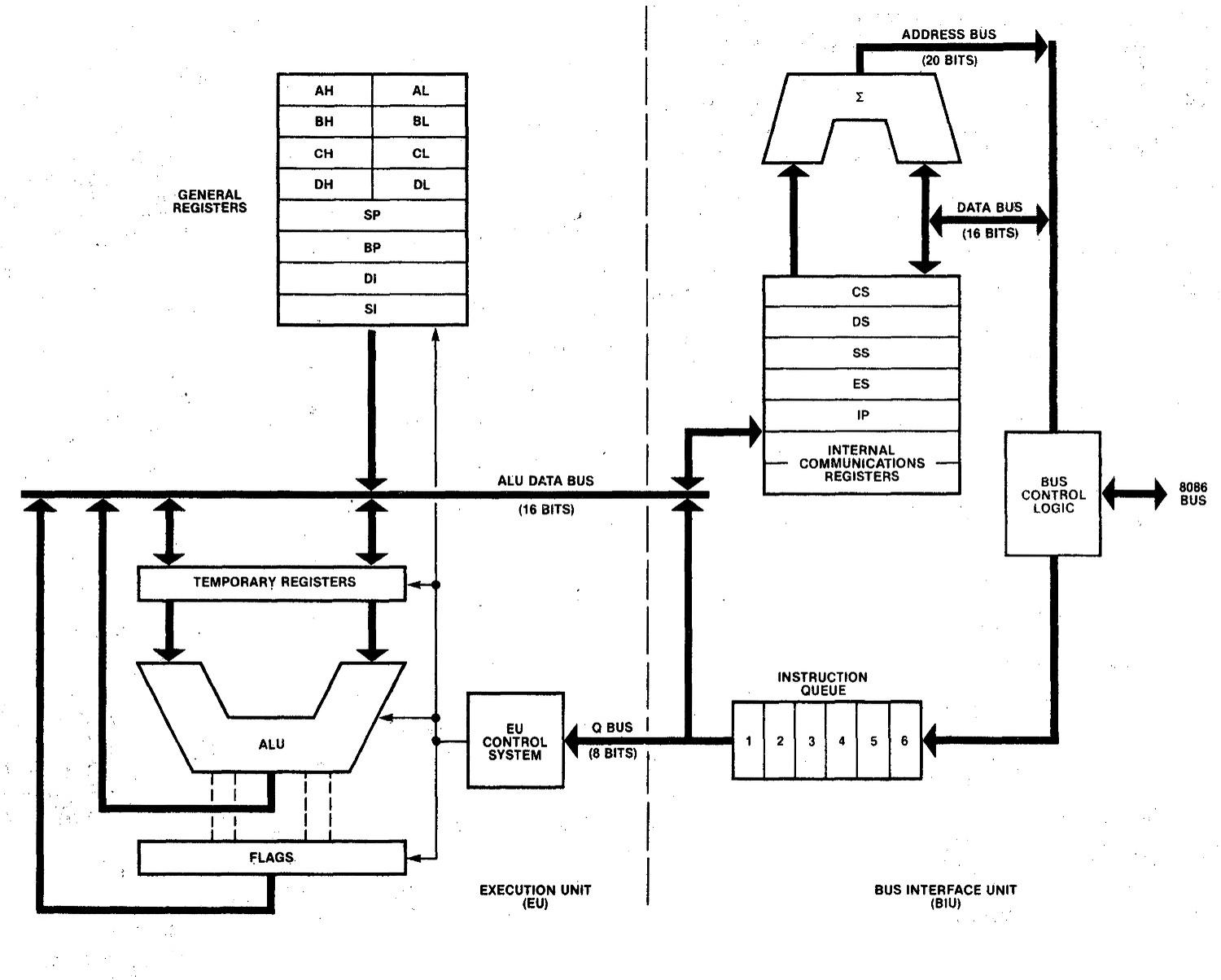
  8. The block diagram below is different from most 8086 block diagrams because it shows the actual physical implementation, rather than the programmer's view of the processor. In particular, this diagram shows two "Internal Communication Registers" in the Bus Interface Unit registers (right) along with the segment registers, matching the 7 registers visible on the die. (The temporary registers below are physically part of the ALU, so I'm not discussing them in this blog post.)

    Block diagram of the 8086 processor. From The 8086 Family User's Manual.

    Block diagram of the 8086 processor. From The 8086 Family User's Manual.


  9. The book Modern Processor Design discusses the complex register systems of processors from the early 2000s. It says that circuit complexity increases rapidly beyond 3 ports, but some high-end processors had register files with 20 ports or more.  

  10. The upper registers have differing numbers of read and write ports, as follows: two registers with 3 read control lines and 2 write lines, one register with 2 read lines and 2 write lines, and four registers with 2 read lines and 1 write line. The first three registers are probably the program counter, the "indirect" temporary register, and the "operand" temporary register. The last four are probably the SS, DS, SS, and ES segment registers. There are also three instruction prefetch buffer registers, each with 1 read line and 1 write line.

    The 8088 processor, used in the original IBM PC was essentially identical to the 8086, except it had an external 8-bit bus instead of a 16-bit bus to reduce system cost. The 8088's prefetch buffer was four bytes instead of six, presumably because four bytes was sufficient with the 8088's slower memory bus.

    Unlike the 8086, the prefetch registers in the 8088 support writing to 8-bit halves independently (similar to the 8088's A, B, C, and D registers, but with a different register cell design). The reason is the 8088 fetched instructions one byte at a time instead of one word at a time, due to its narrower bus. Thus, the 8088's prefetch registers need to support byte-sized writes, while the 8086 does word-sized prefetches. 

  11. I wrote about the 8086 die and the die shrink process earlier. For more about register files, see my posts on registers in the Z-80 and in the 8085

Die shrink: How Intel scaled down the 8086 processor

The revolutionary Intel 8086 microprocessor was introduced 42 years ago this month so I've been studying its die.1 I came across two 8086 dies with different sizes, which reveal details of how a die shrink works. The concept of a die shrink is that as technology improved, a manufacturer could shrink the silicon die, reducing costs and improving performance. But there's more to it than simply scaling down the whole die. Although the internal circuitry can be directly scaled down,2 external-facing features can't shrink as easily. For instance, the bonding pads need a minimum size so wires can be attached, and the power-distribution traces must be large enough for the current. The result is that Intel scaled the interior of the 8086 without change, but the circuitry and pads around the edge of the chip were redesigned.

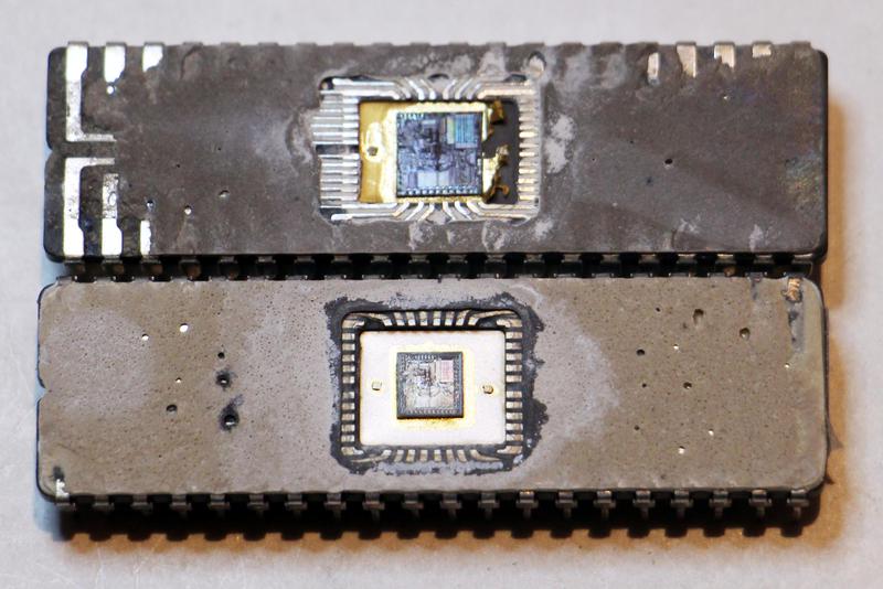
The photo below shows an 8086 chip from 1979, and a version with a visibly smaller die from 1986.3 (The ceramic lids have been removed to show the silicon dies inside.) In the updated 8086, the internal circuitry was scaled to about 64% of the original size by length, so it took 40% of the original area. The die as a whole wasn't reduced as much; it was about 54% of the original area. (The chip's package was unchanged, the 40-pin DIP package commonly used for microprocessors of that era.)

Comparison of two 8086 chips. The newer chip on the bottom has a significantly smaller die. The rectangle in the upper-right of each die is the microcode rom.

Comparison of two 8086 chips. The newer chip on the bottom has a significantly smaller die. The rectangle in the upper-right of each die is the microcode rom.

The 8086 is one of the most influential chips ever created; it started the x86 architecture that still dominates desktop and server computing today. Unlike modern CMOS processors, the 8086 was built from NMOS transistors, as were the 6502, Z-80, and other early processors.4 The first chip was built with HMOS,5, Intel's name for this process. Intel introduced improved HMOS-II in 1979 and in 1982, Intel moved to HMOS-III, the process used for the newer 8086 chip.6 Each newer HMOS version shrunk the size of features on the chip and improved performance.

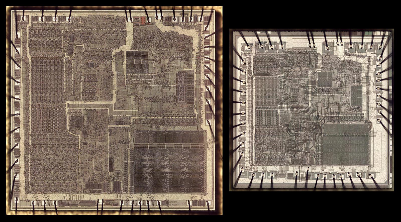
Two versions of the 8086 die, at the same scale. The bond wires are connected to pads around the edge of the die.

Two versions of the 8086 die, at the same scale. The bond wires are connected to pads around the edge of the die.

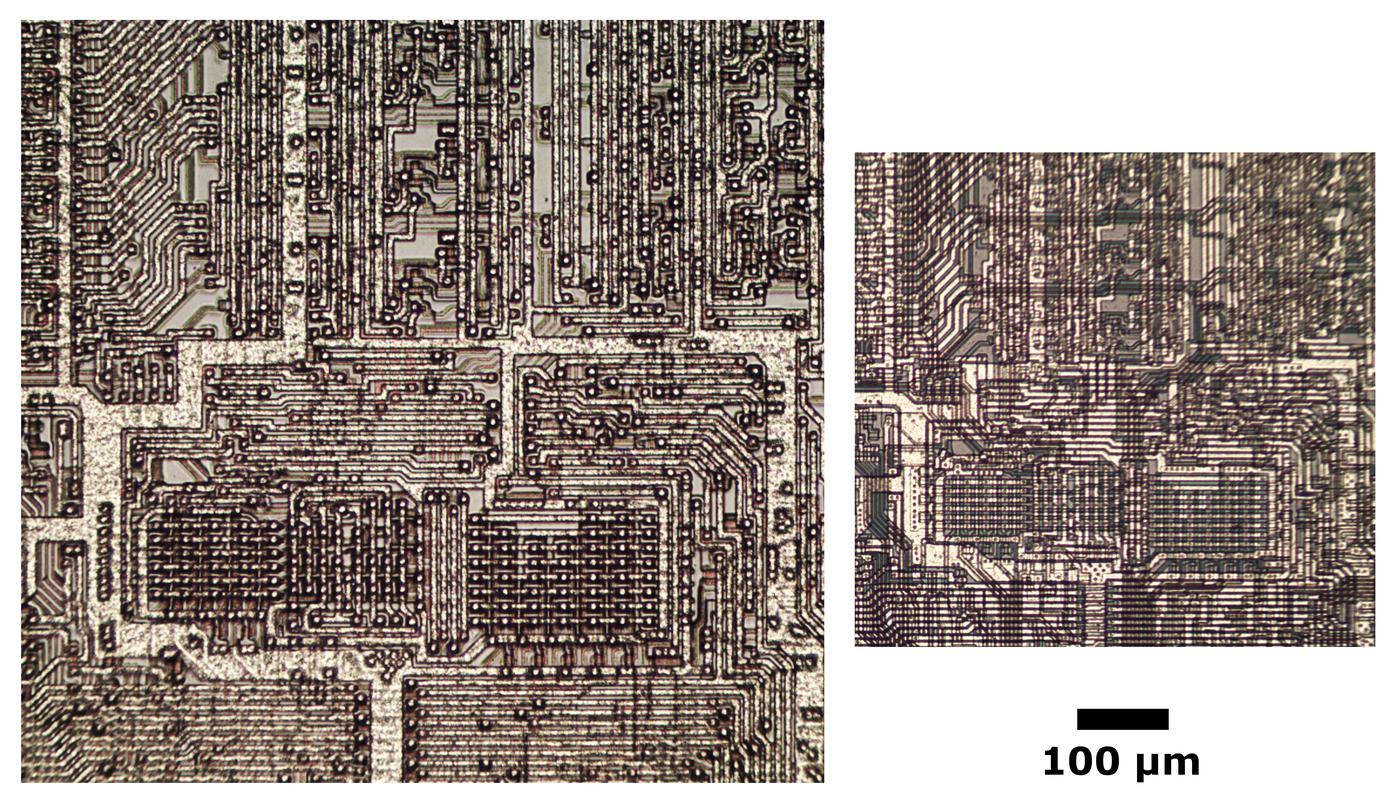
The photo above shows the two 8086 dies at the same scale. The two chips have identical layout in the interior,7 although they may look different at first. The chip on the right has many dark lines in the middle that don't appear on the left, but this is an artifact. These lines are the polysilicon layer, underneath the metal; the die on the left has the same wiring, but it is very faint. I think the newer chip has a thinner metal layer, making the polysilicon more visible.

The magnified photo below shows the same circuitry on the two dies. There is an exact correspondence between components in the two images, showing the circuitry was reduced in size, not redesigned. (These photos show the metal layer on top of the chip; some polysilicon is visible in the right photo.)

The same region of the two dies at the same scale.

The same region of the two dies at the same scale.

However, there are significant differences around the edges of the dies. The bond pads around the outside are closer together, especially in the bottom right. There are two reasons for this. First, the bond pads can't shrink very much, since they need to be large enough to attach bond wires. Second, the power distribution traces around the edges are wider in order to support the necessary current. (Look to the right of the microcode ROM in the lower right, for instance.) Part of this is because the power traces in the middle of the circuitry were scaled down with the rest of the circuitry, so they are smaller; the outside traces need to pick up the slack. In addition, the thinner metal layer in the newer chip can't support as much current without being widened.

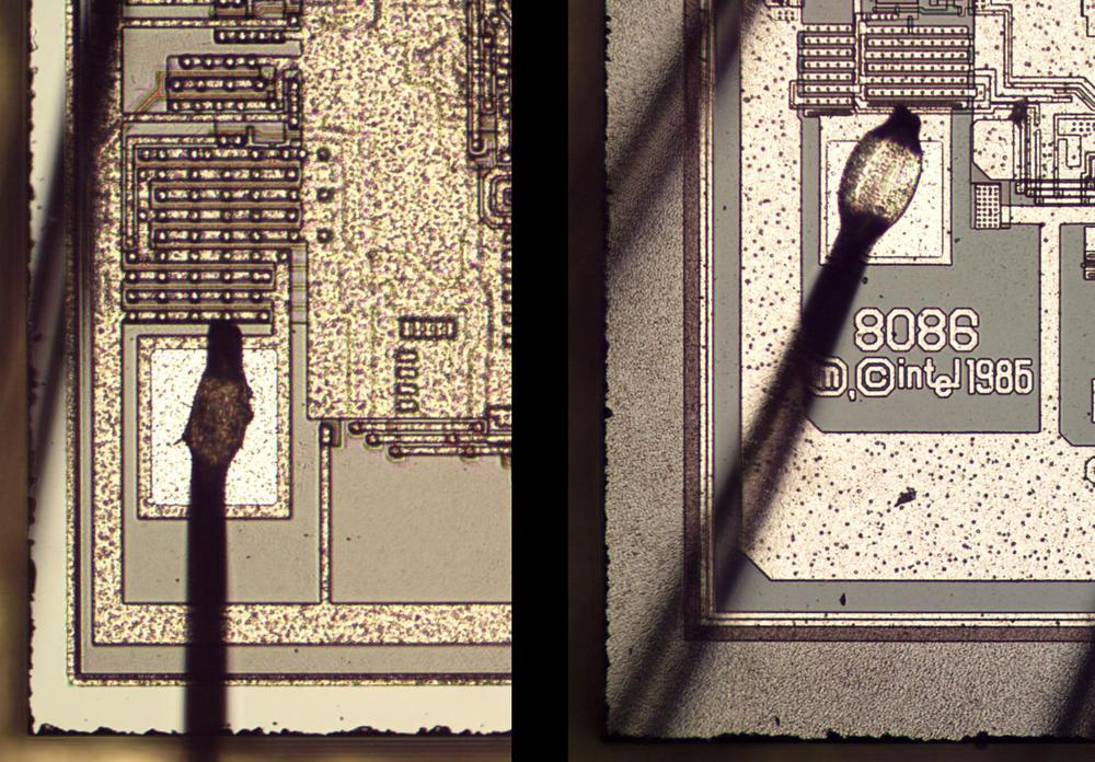
A bond pad and associated transistors, comparing the old chip (left) and new chip (right).
In the copyright date, the top of the "6" is strangely flat; it looks like they changed a "1985" to "1986".

A bond pad and associated transistors, comparing the old chip (left) and new chip (right). In the copyright date, the top of the "6" is strangely flat; it looks like they changed a "1985" to "1986".

The photo above shows a bonding pad with an attached bond wire. The drive transistors are above the pad. The newer chip has almost the same size pad, but the power drive transistors have both shrunk and been redesigned. Note the much thicker metal power wiring on the newer chip. The Intel logo was moved from the bottom right to the bottom left, probably because that's where there was room.

A closer look at the dies

First, a bit of background on the NMOS construction used in the 8086 and other chips of that era. These chips consist of a silicon substrate, which is doped (diffusion) with arsenic or boron to form transistors. On top, a layer of polysilicon creates the gates of the transistors as well as providing wiring between components. Finally, a single metal layer on top wires up the components.

A semiconductor process (such as HMOS-III) has specific rules on the minimum size and spacing for features on the silicon, polysilicon, and metal layers. By looking closely at the chips, we can see how the features correspond to the design rules for HMOS I and HMOS III. The table below (from HMOS III Technology) summarizes the characteristics of the different HMOS processes. The features get smaller and the performance gets better with each version. (Intel got a 40% overall performance improvement going from HMOS-II to HMOS-III.)

 HMOS IHMOS IIHMOS III
Diffusion Pitch (µ)8.06.45.0
Poly Pitch (µ)7.05.64.0
Metal Pitch (µ)11.08.06.4
Gate Oxide Thickness (Ã…)700400250
Channel Length (µ)3.02.01.5
Idsat (mA)8.014.027.0
Minimum Gate-Delay (ps)1000400200
Speed-Power Product (pJ)1.00.50.25
Linear Shrink Factor1.00.80.64

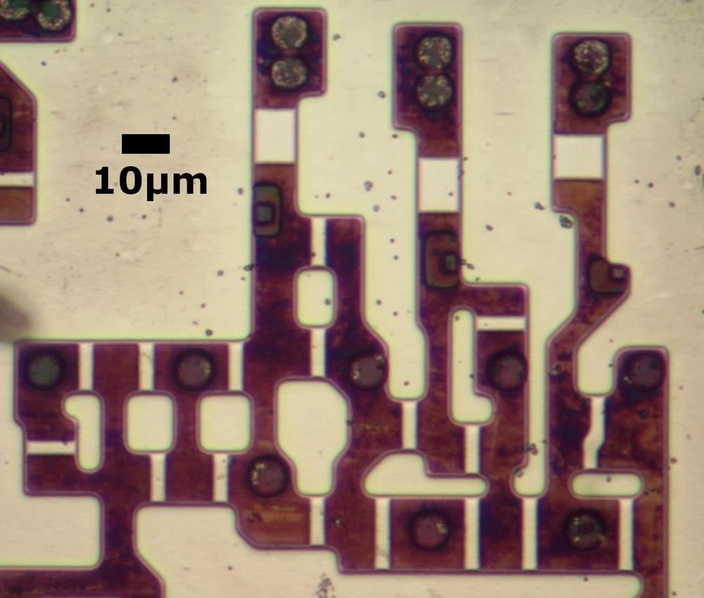
The microscope photo below shows a complex arrangement of transistors in the older 8086 chip. The dark regions are doped silicon, while the white rectangles are the transistor gates. (There are about 21 transistors in this photo.) A key measurement is the channel length, the length of the gate between the source and drain. (This is the narrower dimension of the white rectangles.) I measured 3 μm for these transistors, which nicely matches the published value for HMOS I.8 This indicates the chip was manufactured with a 3 μm process; in comparison, processors are now moving to a 5 nm process, 600 times smaller.

Transistors in the older 8086 chip. The metal and polysilicon were removed for this photo. Circles are vias that connect to the metal layer.

Transistors in the older 8086 chip. The metal and polysilicon were removed for this photo. Circles are vias that connect to the metal layer.

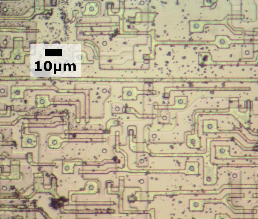
The photo below shows transistors in newer 8086 at the same scale; the transistors are much smaller. The linear dimensions are scaled by 64%, so the transistors have 40% of their original area. Because I processed this die differently, the polysilicon remained on the die, the yellowish lines. The doped silicon appears pinkish, much less visible than before. I measure the gate length as 1.9 μm, which is 64% of the previous 3 μm. Note that HMOS-III supports a considerably smaller 1.5 μm channel length, but since everything shrinks by the same 64% factor, the channel length is larger than necessary. This illustrates that uniformly shrinking the die wastes some of the potential gain from the new process, but it is much easier than completely redesigning the chip.

Transistors in the later 8086 chip. There are many vias between the silicon or polysilicon and the metal (which has been removed).

Transistors in the later 8086 chip. There are many vias between the silicon or polysilicon and the metal (which has been removed).

I also looked at the spacing (pitch) of lines in the metal layer. The photo below shows some horizontal and vertical metal wiring in the older chip. I measured 11μm pitch for the metal lines, which matches the published HMOS I figure. The shrink to 64% yields 7 μm pitch on the new chip, even though HMOS III supported 6.4 μm. As before, the constant shrink factor doesn't take full advantage of the new process.

The metal layer of the older 8086 chip. Reddish polysilicon wiring is visible underneath the metal.

The metal layer of the older 8086 chip. Reddish polysilicon wiring is visible underneath the metal.

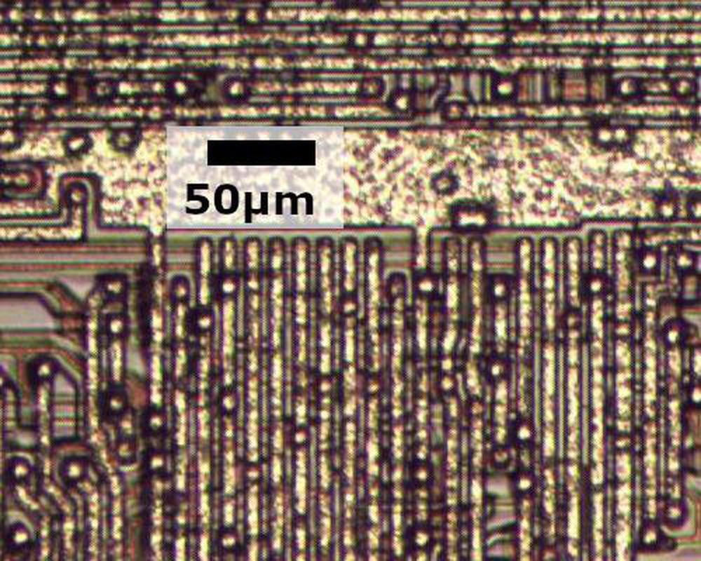
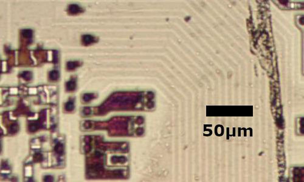
Finally, I looked at the pitch of the polysilicon wiring. The photo below shows the older 8086; the polysilicon has been removed leaving faint white traces. These parallel polysilicon lines probably formed a bus, routing signals from one part of the chip to another. I measured 7 μm pitch for the polysilicon lines, matching the published HMOS figure. (Interestingly, polysilicon wiring can be denser than metal wiring under HMOS rules.) The newer chip has 4.5 μm polysilicon pitch, compared to possible 4.0 μm.

Polysilicon traces on the older 8086 chip.

Polysilicon traces on the older 8086 chip.

Conclusions

A die shrink provides a way to improve the performance of a processor and reduce its cost without the effort of a complete redesign. Comparing the two chips, however, shows that a die shrink is more complex than uniformly shrinking the whole die. While most of the circuitry is a straightforward shrink, the bond pads didn't shrink to the same degree, so they needed to be moved around. The power distribution was also modified, adding more power wiring around the outer part of the chip.

Modern microprocessors still use die shrinks. In 2007, Intel moved to a tick-tock model, where they would alternate shrinks of an existing chip (the "tick") with the production of a new microarchitecture (the "tock").

I plan to analyze the 8086 in more detail in future blog posts so follow me on Twitter at @kenshirriff for updates. I also have an RSS feed.

Notes and references

  1. The 8086 was released on June 8, 1978. 

  2. It's actually quite remarkable that MOSFET circuits still work after being scaled down over a large range, since most things don't scale as easily. For instance, you can't scale down an engine by a factor of 10 and expect it to work. Most physical things suffer from the square-cube law: the area scales with the square of the ratio, while the volume scales with the cube of the ratio. For MOS circuits, however, most things either stay the same with scaling, or get better (such as frequency and power consumption). For more details on scaling, see Mead and Conway's Introduction to VLSI Systems Ch 1 sect 2. Interestingly, that 1978 book says that scaling had a fundamental limit of 1/4 micron (250 nm) channel length due to physical effects. That limit was wildly wrong; transistors are now moving to 5 nm, through technologies such as FinFETs. 

  3. The older chip says ©'78, ©'79 on the package and ©1979 on the die and has a 7947 (47th week of 1979) date code on the underside. The newer chip says ©1978 on the package but ©1986 on the die and has no identifiable date code, so I figure it is from 1986 or slightly later. It's unclear why the newer chip has an older copyright date on the external package. 

  4. A brief description of the technologies in early processors. N-channel MOSFETs are a particular type of MOSFET transistor. They have considerably better performance than the P-channel MOSFETs used in the earliest microprocessors, such as the Intel 4004. (Modern processors use N-channel and P-channel transistors together for lower power consumption; this is CMOS.) Gates built from N-channel MOSFETs require a pull-up resistor, which is implemented by a transistor. Depletion load transistors are a type of transistor introduced in the mid-1970s that perform better as pull-up resistors and don't require an extra power supply voltage. Finally, MOS transistors originally used metal for the gate (the M in MOS). But in the late 1960s, Fairchild developed the use of polysilicon for the gate instead of metal. This provided much better performance and was easier to manufacture. The point of all this is that between the late 1960s and mid-1970s, several radical changes were introduced in MOS integrated circuit production, and these led to the success of the 6502, Z-80, 8085, 8086, and other early processors. In the 1980s, CMOS processors took over due to their lower power consumption and better performance. 

  5. Strangely, it's unclear what the "H" stands for in HMOS. I couldn't find anywhere that Intel expands the acronym; databooks refer to "Intel's advanced N-channel silicon gate HMOS process" or say "HMOS is a high-performance n-channel MOS process". Intel later defined CHMOS as Complementary High Speed Metal Oxide Semiconductor) (example). Motorola defined HMOS as High-density MOS (example) while other sources defined it as High-speed MOS or High-density, short channel MOS. Intel has a patent on "High density/high speed MOS process and device", so perhaps the "H" stands for both "high density" and "high speed". 

  6. Interestingly, Intel used a 4K static RAM chip to develop each of their HMOS processes, before using the process for their microprocessors and other chips. They probably developed with the RAM chip because it has dense circuitry, but is relatively easy to design because it repeats the same memory cell over and over. Once they had all the design rules figured out, then they could create the much more complex processor. 

  7. I scaled complete, high-resolution images of the two chips to compare and the main part of the chips is an exact match except for some trivial changes. I found a couple of places where a via was slightly moved, which is puzzling because I see no logical reason for that. The circuit was unchanged, so it's not a bug fix. One question is if there were any microcode changes. The microcode looks identical, but I didn't do a bit-by-bit comparison. 

  8. You may have noticed that three transistors in the photo have much larger gates. These are transistors that are acting as pull-up resistors, as is typical for NMOS circuits. The larger size makes the transistors weaker, so they provide a weak pull-up current. 

Reverse-engineering and comparing two Game Boy audio amplifier chips

The Nintendo Game Boy contains an audio amplifier chip for sound through a speaker or headphones. In this post, I reverse-engineer this chip and compare it with the later Game Boy Color chip (reverse-engineered earlier). Unexpectedly the Game Boy Color uses an entirely different amplifier design from the original Game Boy, which may explain why the two systems sound different.

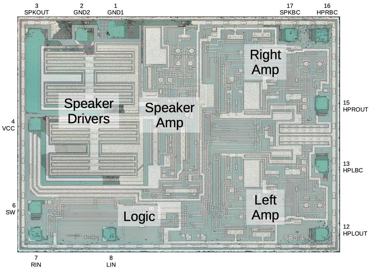
The diagram below shows the Game Boy amplifier's silicon die, with the main functional components labeled.1 The upper-left part of the chip has the two large driver transistors for the speaker output (one to pull the signal low and the other to pull the signal high). The headphone amplifier consists of two nearly-identical blocks: one for the left channel and one for the right. The circuitry for the current sources and current mirrors is shared by both headphone channels. The lower-left of the chip contains digital logic to enable either the speaker amp or the headphone amp, switching when the headphones are plugged in.

The chip with pins and key functional blocks labeled.
The hi-res die photo is courtesy of John McMaster.

The chip with pins and key functional blocks labeled. The hi-res die photo is courtesy of John McMaster.

By examining the die closely, components such as transistors and resistors can be identified. From this, the complete circuit can be determined. In the photo above, the white lines are the chip's metal layer, connecting the components. The silicon itself appears greenish and is underneath the metal. The green squares around the outside are the pads where tiny bond wires connected the silicon die to the chip's 18 pins. Regions of the chip are treated (doped) to change the electrical properties of the silicon. The next sections explain how components are created from these different types of silicon.

NPN transistors

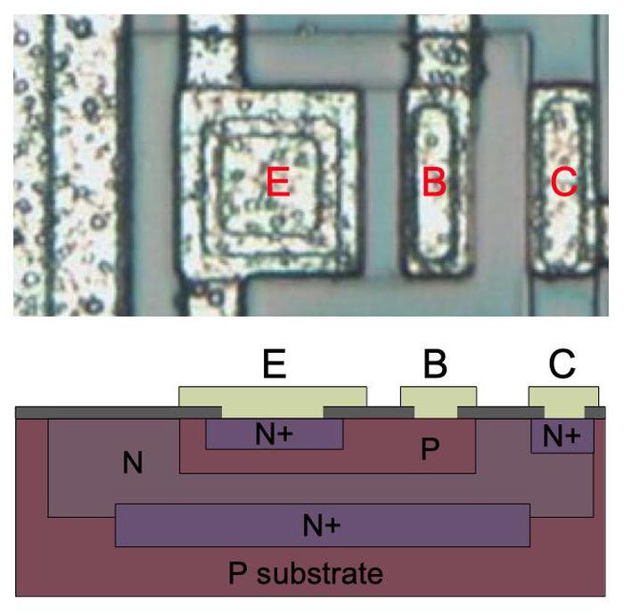
The amplifier chip is built from transistors known as NPN and PNP bipolar transistors, different from the low-power MOS transistors used in processors. These transistors have three connections: the emitter, the base, and the collector. The magnified photo below shows an NPN transistor from above. The slightly different tints in the silicon indicate regions that have been doped to form N and P regions, with dark lines separating the regions. The bubbly silverish areas are the metal layer of the chip on top of the silicon—these form the wires connected to the emitter, base, and collector.

An NPN transistor in the Game Boy Color amplifier chip. The collector (C), emitter (E), and base (B) are labeled, along with N and P doped silicon.

An NPN transistor in the Game Boy Color amplifier chip. The collector (C), emitter (E), and base (B) are labeled, along with N and P doped silicon.

Underneath the photo is a vertical cross-section illustrating how the transistor is constructed. The emitter (E) wire is connected to N+ silicon. Below that is a P layer connected to the base contact (B). And below that is an N+ layer connected (indirectly) to the collector (C). If you look at the vertical cross-section below the 'E', you can find the N-P-N layers that form the transistor.

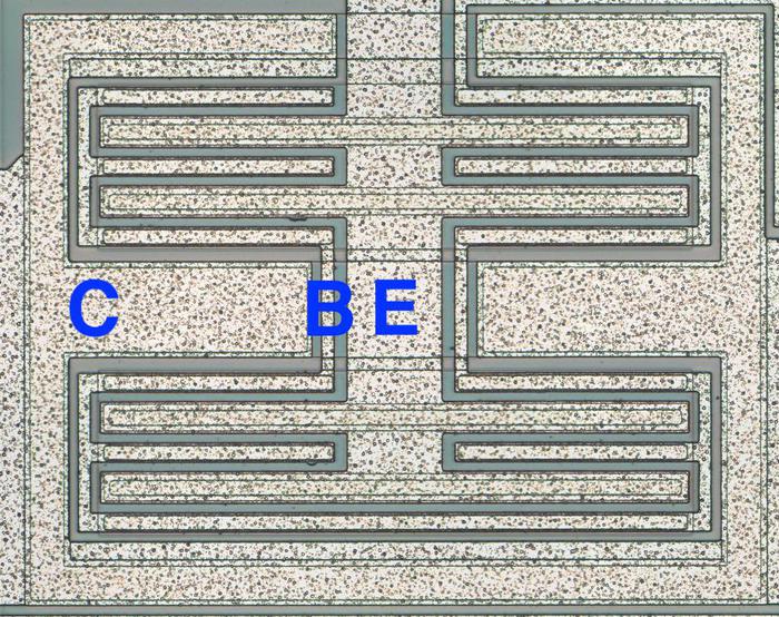
A different structure (below) is used for the high-current output transistors that drive the speaker. These transistors are much larger and have multiple interlocking "fingers" of the emitter and base, surrounded by the large collector. If you look back at the die photo, you can see two of these transistors filling the upper left part of the die.

A large, high-current NPN output transistor in the Game Boy Color audio amplifier chip. The collector (C), base (B), and emitter (E) are labeled.

A large, high-current NPN output transistor in the Game Boy Color audio amplifier chip. The collector (C), base (B), and emitter (E) are labeled.

PNP transistors

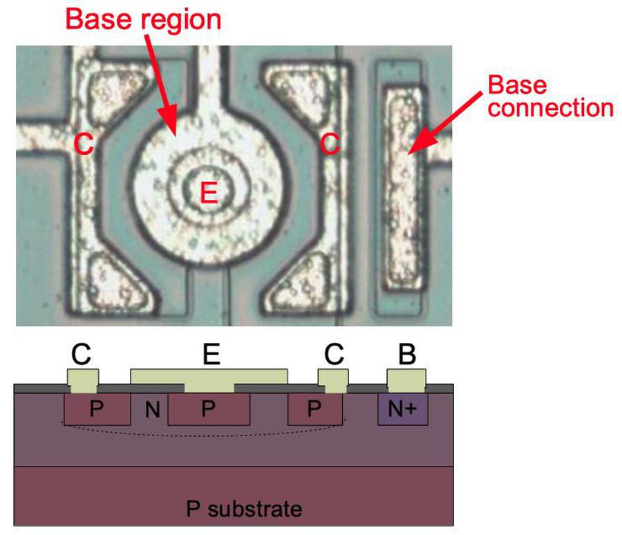
The chip also uses PNP transistors, which have an entirely different construction, as shown in the diagram below. The most obvious difference is that the PNP transistors are round.2 A PNP transistor has a small circular emitter (P-silicon), surrounded by a ring-shaped base region (N-silicon), which in turn is surrounded by the collector (P-silicon). (The emitter metal covers both the emitter and the base, but is only connected to the emitter.) These regions form a P-N-P sandwich horizontally (laterally), unlike the vertical structure of the NPN transistors. Note that although the base region physically surrounds the emitter, the metal connection to the base is further away; the base signal passes through the N region underneath the collector to reach the base region.

A PNP transistor in the Game Boy audio amplifier chip. Connections for the collector (C), emitter (E) and base (B) are labeled, along with N and P doped silicon. The base forms a ring around the emitter, and the collector forms a ring around the base.

A PNP transistor in the Game Boy audio amplifier chip. Connections for the collector (C), emitter (E) and base (B) are labeled, along with N and P doped silicon. The base forms a ring around the emitter, and the collector forms a ring around the base.

Resistors

Resistors are an important component of analog chips. The photo below shows some long, zig-zagging resistors, formed from strips of P silicon, which appears beige in the photo. Its resistance is proportional to the length of the resistor, so large-value resistors have a zig-zag shape to fit in the available space. Because resistors are relatively large and inaccurate, chip designs try to minimize the number of resistors required. Even so, an analog chip like this one requires numerous resistors.

Some resistors in the Game Boy audio amplifier chip. In the center, two resistors in parallel provide a low resistance. The long, meandering resistors provide high resistance.

Some resistors in the Game Boy audio amplifier chip. In the center, two resistors in parallel provide a low resistance. The long, meandering resistors provide high resistance.

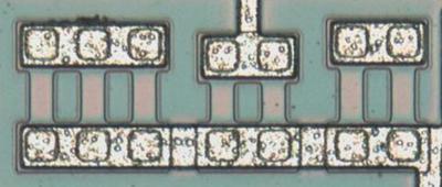
The photo below shows seven small resistors, but only the two in the middle are connected (in parallel) to the circuit. These extra resistors allow the resistance to be modified by modifying the metal layer, which is much easier than changing the silicon. (These resistors bias the output transistor, and it appears this is a critical resistance that required adjustment.)

This photo shows seven short resistors but some are not used.

This photo shows seven short resistors but some are not used.

Capacitors

This chip has three large capacitors, one for each amplifier. The photo below shows one of the capacitors. The capacitors are simply a large layer of metal over the underlying silicon, separated by a thin insulating oxide layer. At the top and right of the photo, you can see the connections between the metal wiring and the underlying silicon. In this chip, capacitors are used to ensure the stability of the amplifiers. Because they are large, the three capacitors are easy to spot in the chip die photo.

A capacitor on the Game Boy audio amplifier chip.

A capacitor on the Game Boy audio amplifier chip.

The LM380

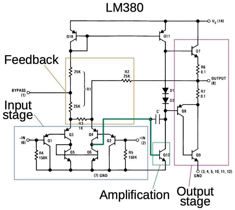
The Game Boy amplifier chip has a design very similar to the popular LM380 power audio amplifier chip (1972), so I'll start with an overview of how the LM380 works. (See the footnote5 for details.) The LM380 has positive and negative inputs and an output that amplifies the difference between the inputs by a fixed factor of 50. This may sound like an op-amp, but the LM380 is intended as an audio amplifier and is different from an op-amp in several ways: it has a small, fixed gain, it doesn't have a negative power supply, and its internal implementation is different.

The schematic below shows the main functional blocks of the LM380. The inputs go into a differential pair circuit (blue)3. The output from the differential pair (green) goes into a single-transistor amplification stage that provides more gain. The capacitor across the amplification stage stabilizes the amplifier to prevent oscillation. Finally, the output stage (purple) produces the high-current output: power transistor Q7 pulls the output high, while Q8 and Q94 pull the output low. The feedback network controls the gain of the LM380, fixing the gain at a factor of 50. Note that unlike an op-amp, the LM380's feedback network is connected to internal points of the amplifier, not the inputs.

The LM380 audio amplifier. Diagram based on the application note.

The LM380 audio amplifier. Diagram based on the application note.

Game Boy Audio chip: headphone amplifier

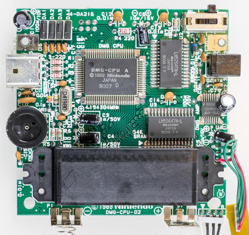
Game Boy circuit board. The audio amplifier chip is midway on the right-hand side. © Raimond Spekking / CC BY-SA 4.0 (via Wikimedia Commons).

Game Boy circuit board. The audio amplifier chip is midway on the right-hand side. © Raimond Spekking / CC BY-SA 4.0 (via Wikimedia Commons).

The Game Boy amplifier chip contains three amplifiers: two identical amplifiers for the left and right headphone channels, and a more powerful mono amplifier for the speaker. The Game Boy headphone amplifiers and the speaker amplifier are somewhat different, but they are both similar to the LM380.

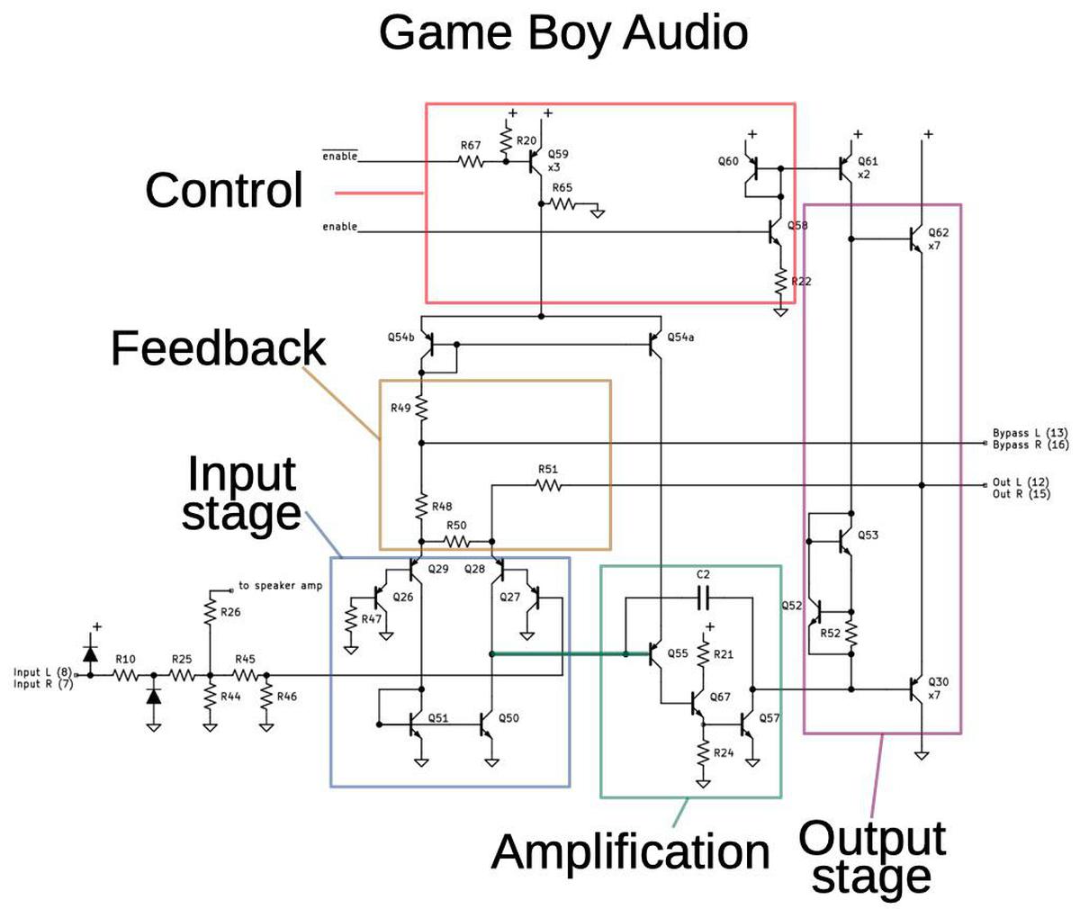
The schematic below shows the Game Boy headphone amplifier. Comparing it with the LM380 schematic above shows the similarities between the LM380 and the headphone amplifier, but also some differences. The input stage and feedback circuit of the LM380 are the most distinctive parts of that chip, and the headphone amplifier's circuit is essentially identical.6 The "Amplification" stage of the headphone amplifier has three transistors compared to one in the LM380, probably to produce more gain. The headphone amplifier's output stage is similar but simplified; the PNP/NPN pair that pulls the LM380 output low is replaced with a single PNP transistor. The biggest difference is the "Control" section of the headphone amplifier, which is not present in the LM380. This control circuitry powers down the headphone amplifier if headphones are not plugged in, conserving battery life.

Schematic of the Game Boy headphone amplifier that I created by reverse-engineering the die.

Schematic of the Game Boy headphone amplifier that I created by reverse-engineering the die.

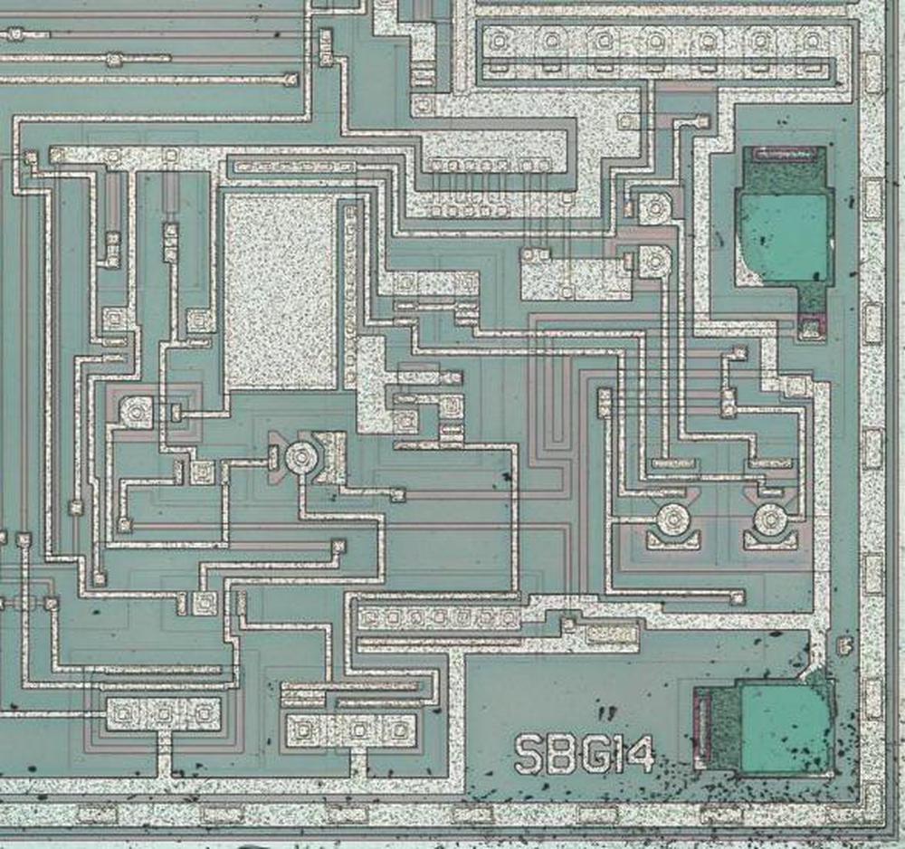
The photo below shows the left headphone amplifier. The output pin (lower-right, next to the part number SBG14) is driven by seven PNP transistors in parallel (top-left) and seven smaller NPN transistors in parallel (lower center). The capacitor is in the upper left, near the center. Many resistors snake around the die.

The left headphone amplifier circuit on the die. The right amplifier is a mirror image. Photo courtesy of John Mcmaster.

The left headphone amplifier circuit on the die. The right amplifier is a mirror image. Photo courtesy of John Mcmaster.

Game Boy Audio chip: speaker amplifier

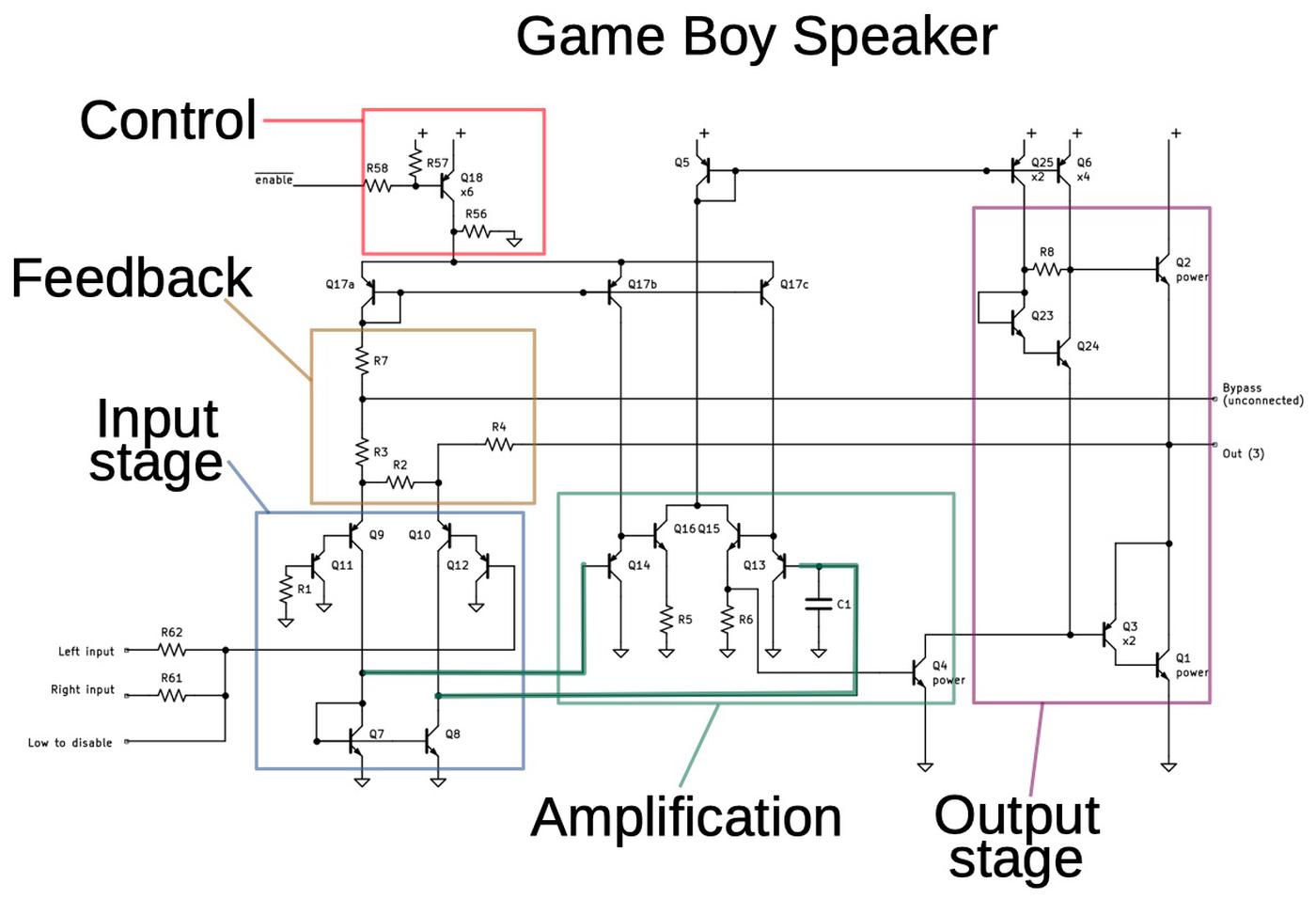
The next schematic shows the Game Boy speaker amplifier. Unlike the two channels for headphone amplification, there is a single speaker amplifier, producing a mixture of the left and right channels. Again, the input stage and feedback are almost identical to the LM380. The output stage has only minor differences. However, the amplification stage for the speaker is completely different: it includes a four-transistor differential amplifier stage, which will provide much more amplification.7 Although this amplification stage looks very similar to the input stage at first glance, its is wired differently and uses NPN transistors.8

Schematic of the speaker amplifier in the Game Boy audio amplifier chip.

Schematic of the speaker amplifier in the Game Boy audio amplifier chip.

The chip provides pins for bypass capacitors to reduce the effect of power supply fluctuations.9 The headphone amplifiers have external bypass capacitors, but the speaker bypass capacitor is omitted for some reason (see the Game Boy schematic). Lack of this capacitor may contribute to the background hum that people hear in the Game Boy's sound.

Comparison with the Game Boy Color

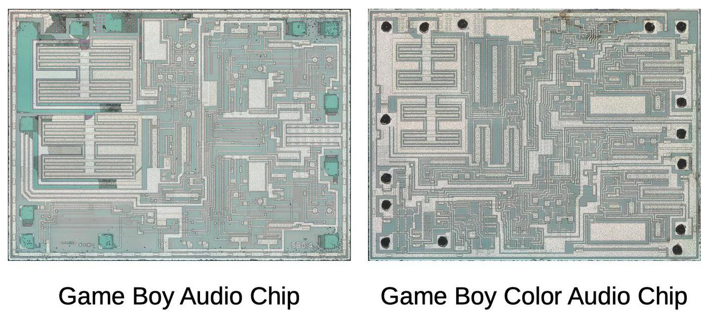
I recently reverse-engineered the Game Boy Color's amplifier chip, so it's interesting to compare the two chips. The amplifier chips for the Game Boy and the Game Boy Color provide similar functions. Even at the die level (below), the two chips look similar. They both have power transistors in the upper-left for the speaker, control circuitry in the lower-left, and two headphone channels on the right.

Comparison of the audio amplifier chip from the Game Boy (left) and Game Boy Color (right). Photos courtesy of John McMaster.

Comparison of the audio amplifier chip from the Game Boy (left) and Game Boy Color (right). Photos courtesy of John McMaster.

Surprisingly, the implementations of the two chips are completely different. While the Game Boy uses LM380-style audio amplifiers, the Game Boy Color uses power op-amps with more complicated circuitry. The most important difference is that the Game Boy chip has internal feedback to control the gain, while the Game Boy Color also has an external feedback capacitor, which causes it to act as a high-pass filter. For more information, see my Game Boy Color amplifier article and schematic.

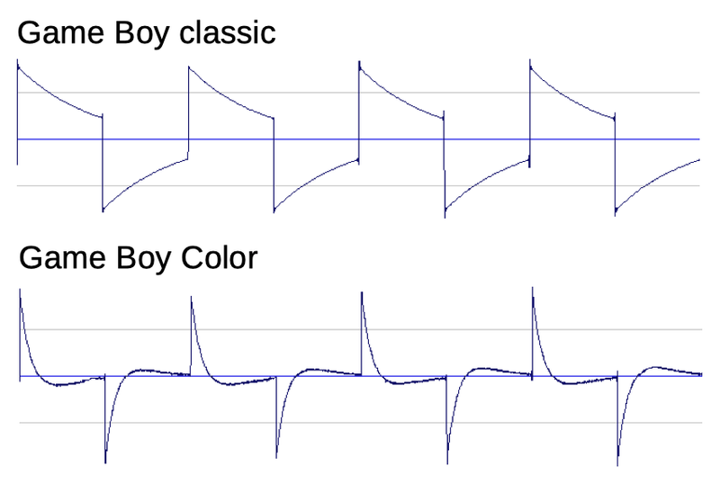
Collectors of Game Boy systems have noticed that the different versions have a very different sound (discussion). The original Game Boy has a "warm, bassy sound", while the Game Boy Color has a "thin sound" with background noise and hum. These aren't just subjective differences, but show up in the waveforms:

Graphs courtesy of Herbert Weixelbaum.

Graphs courtesy of Herbert Weixelbaum.

What's interesting is that we can explain much of the sound difference through the analysis of the amplifier chips. The Game Boy's output is close to a square wave, but the waveform drops somewhat due to the speaker's 100µF DC blocking capacitor (schematic). The amplifier in the Game Boy Color, on the other hand, is configured as a high-pass filter, so it outputs higher-frequency spikes, losing the bass sound.

Conclusion

The Game Boy (1989) and Game Boy Color (1998) use custom amplifier chips. By examining die photos, the circuitry can be reverse engineered. The chips are different from common amplifier chips in two main ways, which probably explains why custom chips were created. First, each chip has three amplifiers: two for headphone channels and one for the speaker. Second, to conserve power the chip has circuitry to power-down the unused amplifiers, based on whether or not headphones are plugged in. Reverse-engineering the chips also explains much of the difference in sound between the Game Boy and the Game Boy Color. The Game Boy Color's chip implements a high-pass filter, so the sound is thin and lacks the bass of the Game Boy.

I announce my latest blog posts on Twitter, so follow me @kenshirriff for future articles. I also have an RSS feed. My KiCad files for the schematic are on Github. Thanks to John McMaster for providing the chip photos; his page is here. Thanks to Herbert Weixelbaum for the sound waveforms.

Notes and references

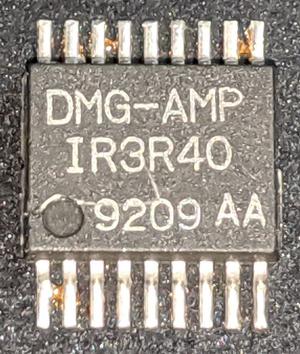
  1. The audio amplifier chip is labeled DMG-AMP, standing for "Dot Matrix Game amplifier". The part number on this 18-pin chip (made by Sharp) is IR3R40.

    The IR3R40 chip. Photo courtesy of John McMaster.

    The IR3R40 chip. Photo courtesy of John McMaster.

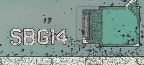
    Internally, the chip is labeled SBG14.

    The die is labeled SBG14.

    The die is labeled SBG14.

  2. Most of the PNP transistors on this chip are round. However, when multiple PNP transistors are combined, a square structure is used instead. The square PNP transistors are larger than the square NPN transistors. The chip also has some PNP transistors with multiple collectors. Other PNP transistors have no explicit collector connection but use the substrate (ground). 

  3. The inputs to the LM380 (or Game Boy amplifier) go into a differential pair (Q3, Q4), but this differential pair is different from the standard one used in op-amps. In particular, the emitters receive different, varying currents, and this is where the feedback happens. 

  4. The output stages of the LM380 and the Game Boy speaker amplifier use two transistors for pull-down configured as a Szilaki pair. The combined PNP and NPN transistors act as a higher-performance PNP transistor, somewhat like a Darlington pair. 

  5. The LM380 is explained in detail in the National Semiconductor application note, and Power Audio Amplifier IC LM380. The similar LM386 is discussed in LM386 lecture and LM386 adventures.

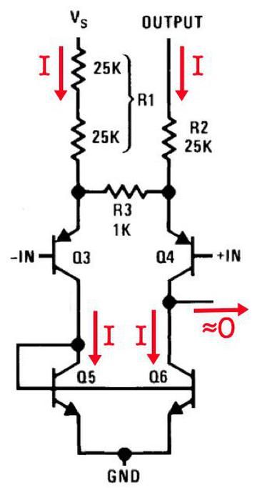
    I'll explain the feedback network since the Game Boy chip operates the same way. The diagram below shows how the feedback network in the LM380 operates with no input. In the upper left, the supply voltage VS across R1 creates a current I. Transistors Q5 and Q6 form a current mirror: this forces the current through Q6 to match the current (I) through Q5. The current from Q4 to the rest of the chip must be approximately 0 (since it is strongly amplified by the rest of the chip). Putting this all together, the current through R2 (generated from the output voltage feedback) must also be I. Since R2 is half the resistance of R1, the output voltage must be half of the supply voltage. The conclusion is that the output voltage at idle will be half of the supply voltage, as desired.

    The LM380 with no signal applied. Schematic of the amplifier feedback network, from the LM380 datasheet.

    The LM380 with no signal applied. Schematic of the amplifier feedback network, from the LM380 datasheet.

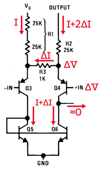
    When inputs are applied, the feedback network acts as seen below. Suppose a voltage ΔV is applied to the positive input. Emitter-follower transistors Q3 and Q4 buffer and raise the inputs, so the same ΔV appears across resistor R3. This generates a current ΔI through the resistor. This increases the current through Q5 to I+ΔI, and because of the current mirror, the same current will flow through Q6. Adding up the various currents, the current through R2 must be I+2ΔI. Since R2 has 25 times the resistance of R3, 2ΔI corresponds to an increase in the output voltage of 50ΔV. Therefore, the input voltage is multiplied by a factor of 50. The point of this is that the feedback network fixes the gain at 50.

    The LM380 with a small signal applied.

    The LM380 with a small signal applied.

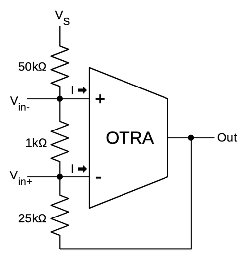
    It seems to me that the best way to understand the LM380 is to consider it as constructed from an operational transresistance amplifier (OTRA), an obscure relative of the op-amp. An OTRA acts like an op-amp, except the two inputs are currents instead of voltages, and the difference between the currents is amplified to produce the output voltage. The two currents (I) into the OTRA must be approximately equal, but the input voltages can diverge (unlike an op-amp).

    My simplified schematic of the LM380, using an operational transresistance amplifier.

    My simplified schematic of the LM380, using an operational transresistance amplifier.

    The schematic above shows the LM380's circuitry represented as an operational transconductance amplifier and feedback network. Equating the two currents yields Vout = Vs/2 + 51V+ - 50.5V- or approximately Vout = Vs/2 + 50*(V+-V-). In other words, the output is centered at half the supply voltage, and the difference in input voltages is amplified by a factor of 50. (Nobody else describes the LM380 in this way, so it's quite possible that I am looking at it wrong, but this analysis makes sense to me.) 

  6. I don't know the exact values of the resistances on the die, but by comparing lengths on the die I can determine ratios of resistances. Looking at resistors R48, R49, R50, and R51, I calculate that the speaker amplifier has a gain factor of 22. From resistors R2, R3, R4, and R7, I calculate that the speaker amplifier has a gain factor of 30, significantly more than the headphone amplifiers. 

  7. Note that the overall amplification of the chip is limited by the feedback network. The idea of an op-amp is the raw gain will be something like 100,000, but the feedback reduces the gain to something reasonable like a factor of 50. The "extra" gain improves performance and reduces distortion. In other words, the additional amplification stage in the Game Boy compared to the LM380 isn't going to make it 100 times louder. 

  8. I'm a bit puzzled by the second amplification stage for the speaker amplifier. It looks like a differential amplifier, except a differential amplifier normally has the emitters connected and this circuit has the collectors connected. 

  9. The bypass capacitors used by the Game Boy chip (and the LM380) help reduce the impact of power supply fluctuations. It's common for chips to have a bypass capacitor between power and ground, but this bypass capacitor is a bit different. It is connected to a point in the feedback network where it is more effective than a regular bypass capacitor. 

A look at the die of the 8086 processor

The Intel 8086 microprocessor was introduced 42 years ago this month,1 so I made some high-res die photos of the chip to celebrate. The 8086 is one of the most influential chips ever created; it started the x86 architecture that still dominates desktop and server computing today. By looking at the chip's silicon, we can see the internal features of this chip.

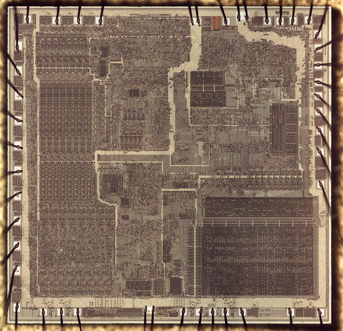
The photo below shows the die of the 8086. In this photo, the chip's metal layer is visible, mostly obscuring the silicon underneath. Around the edges of the die, thin bond wires provide connections between pads on the chip and the external pins. (The power and ground pads each have two bond wires to support the higher current.) The chip was complex for its time, containing 29,000 transistors.

Die photo of the 8086, showing the metal layer. Around the edges, bond wires are connected to pads on the die. Click for a large, high-resolution image.

Die photo of the 8086, showing the metal layer. Around the edges, bond wires are connected to pads on the die. Click for a large, high-resolution image.

Looking inside the chip

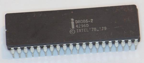
To examine the die, I started with the 8086 integrated circuit below. Most integrated circuits are packaged in epoxy, so dangerous acids are necessary to dissolve the package. To avoid that, I obtained the 8086 in a ceramic package instead. Opening a ceramic package is a simple matter of tapping it along the seam with a chisel, popping the ceramic top off.

The 8086 chip, in 40-pin ceramic DIP package.

The 8086 chip, in 40-pin ceramic DIP package.

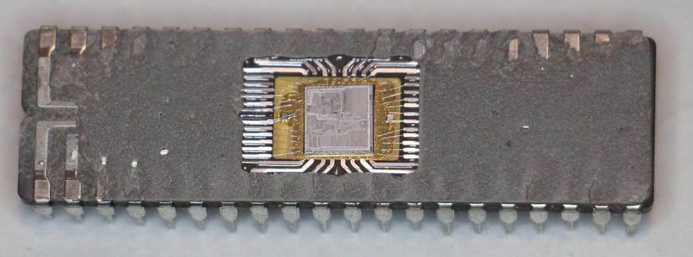
With the top removed, the silicon die is visible in the center. The die is connected to the chip's metal pins via tiny bond wires. This is a 40-pin DIP package, the standard packaging for microprocessors at the time. Note that the silicon die itself occupies a small fraction of the chip's size.

The 8086 die is visible in the middle of the integrated circuit package.

The 8086 die is visible in the middle of the integrated circuit package.

Using a metallurgical microscope, I took dozens of photos of the die and stitched them into a high-resolution image using a program called Hugin (details). The photo at the beginning of the blog post shows the metal layer of the chip, but this layer hid the silicon underneath.

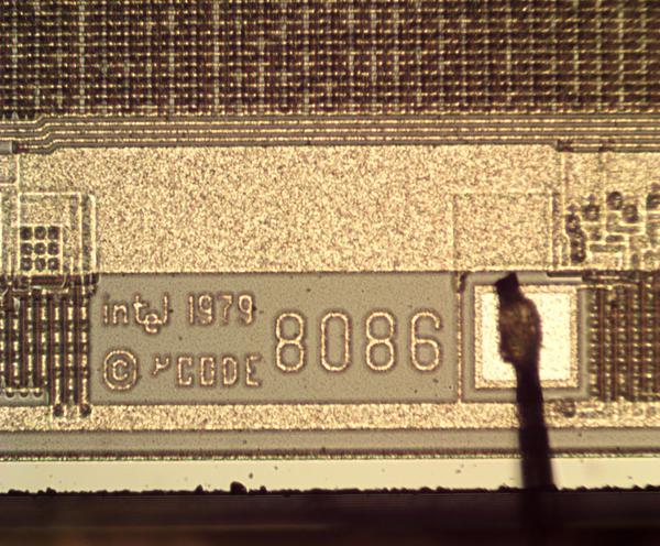
Under the microscope, the 8086 part number is visible as well as the copyright date. A bond wire is connected to a pad. Part of the microcode ROM is at the top.

Under the microscope, the 8086 part number is visible as well as the copyright date. A bond wire is connected to a pad. Part of the microcode ROM is at the top.

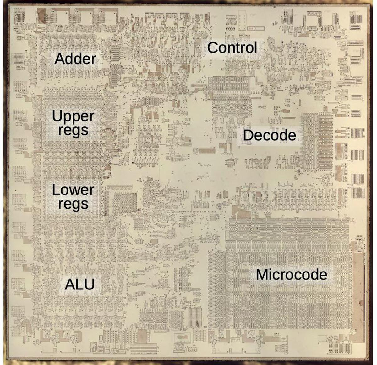
For the die photo below, the metal and polysilicon layers were removed, showing the underlying silicon with its 29,000 transistors.2 The labels show the main functional blocks, based on my reverse engineering. The left side of the chip contains the 16-bit datapath: the chip's registers and arithmetic circuitry. The adder and upper registers form the Bus Interface Unit that communicates with external memory, while the lower registers and the ALU form the Execution Unit that processes data. The right side of the chip has control circuitry and instruction decoding, along with the microcode ROM that controls each instruction.

Die of the 8086 microprocessor showing main functional blocks.

Die of the 8086 microprocessor showing main functional blocks.

One feature of the 8086 was instruction prefetching, which improved performance by fetching instructions from memory before they were needed. This was implemented by the Bus Interface Unit in the upper left, which accessed external memory. The upper registers include the 8086's infamous segment registers, which provided access to a larger address space than the 64 kilobytes allowed by a 16-bit address. For each memory access, a segment register and a memory offset were added to form the final memory address. For performance, the 8086 had a separate adder for these memory address computations, rather than using the ALU. The upper registers also include six bytes of instruction prefetch buffer and the program counter.

The lower-left corner of the chip holds the Execution Unit, which performs data operations. The lower registers include the general-purpose registers and index registers such as the stack pointer. The 16-bit ALU performs arithmetic operations (addition and subtraction), Boolean logical operations, and shifts. The ALU does not implement multiplication or division; these operations are performed through a sequence of shifts and adds/subtracts, so they are relatively slow.

Microcode

One of the hardest parts of computer design is creating the control logic that tells each part of the processor what to do to carry out each instruction. In 1951, Maurice Wilkes came up with the idea of microcode: instead of building the control logic from complex logic gate circuitry, the control logic could be replaced with special code called microcode. To execute an instruction, the computer internally executes several simpler micro-instructions, which are specified by the microcode. With microcode, building the processor's control logic becomes a programming task instead of a logic design task.

Microcode was common in mainframe computers of the 1960s, but early microprocessors such as the 6502 and Z-80 didn't use microcode because early chips didn't have room to store microcode. However, later chips such as the 8086 and 68000, used microcode, taking advantage of increasing chip densities. This allowed the 8086 to implement complex instructions (such as multiplication and string copying) without making the circuitry more complex. The downside was the microcode took a large fraction of the 8086's die; the microcode is visible in the lower-right corner of the die photos.3

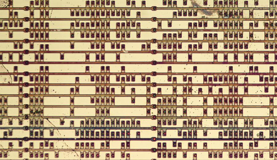
A section of the microcode ROM. Bits are stored by the presence or absence of transistors. The transistors are the small white rectangles above and/or below each dark rectangle. The dark rectangles are connections to the horizontal output buses in the metal layer.

A section of the microcode ROM. Bits are stored by the presence or absence of transistors. The transistors are the small white rectangles above and/or below each dark rectangle. The dark rectangles are connections to the horizontal output buses in the metal layer.

The photo above shows part of the microcode ROM. Under a microscope, the contents of the microcode ROM are visible, and the bits can be read out, based on the presence or absence of transistors in each position. The ROM consists of 512 micro-instructions, each 21 bits wide. Each micro-instruction specifies movement of data between a source and destination. It also specifies a micro-operation which can be a jump, ALU operation, memory operation, microcode subroutine call, or microcode bookkeeping. The microcode is fairly efficient; a simple instruction such as increment or decrement consists of two micro-instructions, while a more complex string copy instruction is implemented in eight micro-instructions.3

History of the 8086

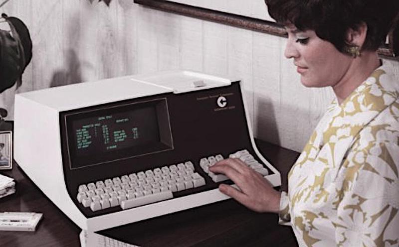
The path to the 8086 was not as direct and planned as you might expect. Its earliest ancestor was the Datapoint 2200, a desktop computer/terminal from 1970. The Datapoint 2200 was before the creation of the microprocessor, so it used an 8-bit processor built from a board full of individual TTL integrated circuits. Datapoint asked Intel and Texas Instruments if it would be possible to replace that board of chips with a single chip. Copying the Datapoint 2200's architecture, Texas Instruments created the TMX 1795 processor (1971) and Intel created the 8008 processor (1972). However, Datapoint rejected these processors, a fateful decision. Although Texas Instruments couldn't find a customer for the TMX 1795 processor and abandoned it, Intel decided to sell the 8008 as a product, creating the microprocessor market. Intel followed the 8008 with the improved 8080 (1974) and 8085 (1976) processors. (I've written more about early microprocessors here.)

Datapoint 2200 computer. Photo courtesy of Austin Roche.

Datapoint 2200 computer. Photo courtesy of Austin Roche.

In 1975, Intel's next big plan was the 8800 processor designed to be Intel's chief architecture for the 1980s. This processor was called a "micromainframe" because of its planned high performance. It had an entirely new instruction set designed for high-level languages such as Ada, and supported object-oriented programming and garbage collection at the hardware level. Unfortunately, this chip was too ambitious for the time and fell drastically behind schedule. It eventually launched in 1981 (as the iAPX 432) with disappointing performance, and was a commercial failure.

Because the iAPX 432 was behind schedule, Intel decided in 1976 that they needed a simple, stop-gap processor to sell until the iAPX 432 was ready. Intel rapidly designed the 8086 as a 16-bit processor somewhat compatible with the 8-bit 8080,4 released in 1978. The 8086 had its big break with the introduction of the IBM Personal Computer (PC) in 1981. By 1983, the IBM PC was the best-selling computer and became the standard for personal computers. The processor in the IBM PC was the 8088, a variant of the 8086 with an 8-bit bus. The success of the IBM PC made the 8086 architecture a standard that still persists, 42 years later.

Why did the IBM PC pick the Intel 8088 processor?7 According to Dr. David Bradley, one of the original IBM PC engineers, a key factor was the team's familiarity with Intel's development systems and processors. (They had used the Intel 8085 in the earlier IBM Datamaster desktop computer.) Another engineer, Lewis Eggebrecht, said the Motorola 68000 was a worthy competitor6 but its 16-bit data bus would significantly increase cost (as with the 8086). He also credited Intel's better support chips and development tools.5

In any case, the decision to use the 8088 processor cemented the success of the x86 family. The IBM PC AT (1984) upgraded to the compatible but more powerful 80286 processor. In 1985, the x86 line moved to 32 bits with the 80386, and then 64 bits in 2003 with AMD's Opteron architecture. The x86 architecture is still being extended with features such as AVX-512 vector operations (2016). But even though all these changes, the x86 architecture retains compatibility with the original 8086.

Transistors

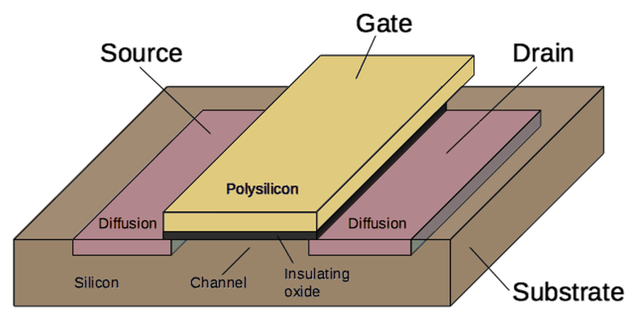
The 8086 chip was built with a type of transistor called NMOS. The transistor can be considered a switch, controlling the flow of current between two regions called the source and drain. These transistors are built by doping areas of the silicon substrate with impurities to create "diffusion" regions that have different electrical properties. The transistor is activated by the gate, made of a special type of silicon called polysilicon, layered above the substrate silicon. The transistors are wired together by a metal layer on top, building the complete integrated circuit. While modern processors may have over a dozen metal layers, the 8086 had a single metal layer.

Structure of a MOSFET in the integrated circuit.

Structure of a MOSFET in the integrated circuit.

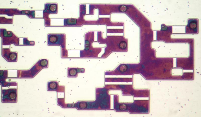
The closeup photo of the silicon below shows some of the transistors from the arithmetic-logic unit (ALU). The doped, conductive silicon has a dark purple color. The white stripes are where a polysilicon wire crossed the silicon, forming the gate of a transistor. (I count 23 transistors forming 7 gates.) The transistors have complex shapes to make the layout as efficient as possible. In addition, the transistors have different sizes to provide higher power where needed. Note that neighboring transistors can share the source or drain, causing them to be connected together. The circles are connections (called vias) between the silicon layer and the metal wiring, while the small squares are connections between the silicon layer and the polysilicon.

Closeup of some transistors in the 8086. The metal and polysilicon layers have been removed in this photo. The doped silicon has a dark purple appearance due to thin-film interference.

Closeup of some transistors in the 8086. The metal and polysilicon layers have been removed in this photo. The doped silicon has a dark purple appearance due to thin-film interference.

Conclusions

The 8086 was intended as a temporary stop-gap processor until Intel released their flagship iAPX 432 chip, and was the descendant of a processor built from a board full of TTL chips. But from these humble beginnings, the 8086's architecture (x86) unexpectedly ended up dominating desktop and server computing until the present.

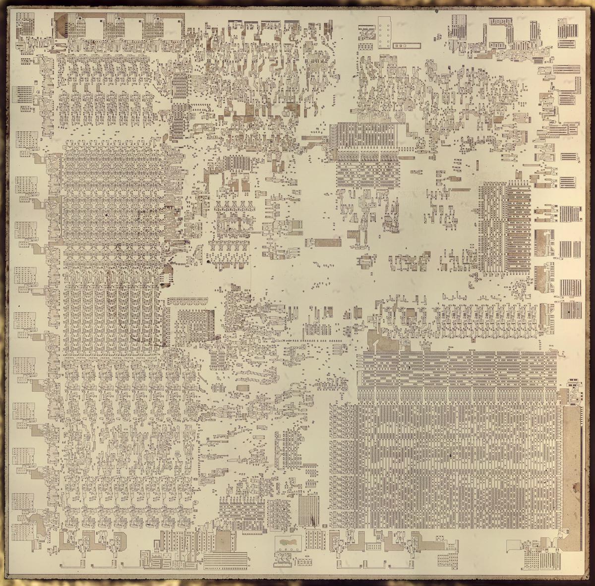
Although the 8086 is a complex chip, it can be examined under a microscope down to individual transistors. I plan to analyze the 8086 in more detail in future blog posts8, so follow me on Twitter at @kenshirriff for updates. I also have an RSS feed. Here's a bonus high-resolution photo of the 8086 with the metal and polysilicon removed; click for a large version.

Die photo of the Intel 8086 processor. The metal and polysilicon have been removed to reveal the underlying silicon.

Die photo of the Intel 8086 processor. The metal and polysilicon have been removed to reveal the underlying silicon.

Notes and references

  1. The 8086 was released on June 8, 1978. 

  2. To expose the chip's silicon, I used Armour Etch glass etching cream to remove the silicon dioxide layer. Then I dissolved the metal using hydrochloric acid (pool acid) from the hardware store. I repeated these steps until the bare silicon remained, revealing the transistors. 

  3. The designers of the 8086 used several techniques to keep the size of the microcode manageable. For instance, instead of implementing separate microcode routines for byte operations and word operations, they re-used the microcode and implemented control circuitry (with logic gates) to handle the different sizes. Similarly, they used the same microcode for increment and decrement instructions, with circuitry to add or subtract based on the opcode. The microcode is discussed in detail in New options from big chips and patent 4449184

  4. The 8086 was designed to provide an upgrade path from the 8080, but the architectures had significant differences, so they were not binary compatible or even compatible at the assembly code level. Assembly code for the 8080 could be converted to 8086 assembly via a program called CONV-86, which would usually require manual cleanup afterward. Many of the early programs for the 8086 were conversions of 8080 programs. 

  5. Eggebrecht, one of the original engineers on the IBM PC, discusses the reasons for selecting the 8088 in Interfacing to the IBM Personal Computer (1990), summarized here. He discussed why other chips were rejected: IBM microprocessors lacked good development tools, and 8-bit processors such as the 6502 or Z-80 had limited performance and would make IBM a follower of the competition. I get the impression that he would have preferred the Motorola 68000. He concludes, "The 8088 was a comfortable solution for IBM. Was it the best processor architecture available at the time? Probably not, but history seems to have been kind to the decision." 

  6. The Motorola 68000 processor was a 32-bit processor internally, with a 16-bit bus, and is generally considered a more advanced processor than the 8086/8088. It was used in systems such as Sun workstations (1982), Silicon Graphics IRIS (1984), the Amiga (1985), and many Apple systems. Apple used the 68000 in the original Apple Macintosh (1984), upgrading to the 68030 in the Macintosh IIx (1988), and the 68040 with the Macintosh Quadra (1991). However, in 1994, Apple switched to the RISC PowerPC chip, built by an alliance of Apple, IBM, and Motorola. In 2006, Apple moved to Intel x86 processors, almost 28 years after the introduction of the 8086. Now, Apple is rumored to be switching from Intel to its own ARM-based processors. 

  7. For more information on the development of the IBM PC, see A Personal History of the IBM PC by Dr. Bradley. 

  8. The main reason I haven't done more analysis of the 8086 is that I etched the chip for too long while removing the metal and removed the polysilicon as well, so I couldn't photograph and study the polysilicon layer. Thus, I can't determine how the 8086 circuitry is wired together. I've ordered another 8086 chip to try again.