Looking inside a vintage Soviet TTL logic integrated circuit

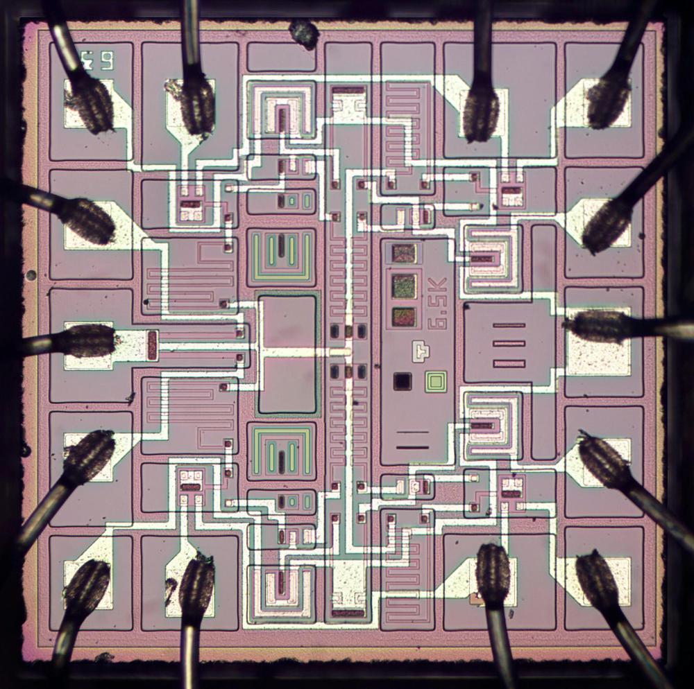
This blog post examines a 1980s chip used in a Soyuz space clock. The microscope photo below shows the tiny silicon die inside the package, with a nice, geometric layout. The silicon appears pinkish or purplish in this photo, while the metal wiring layer on top is white. Around the edge of the chip, the bond wires (black) connect pads on the chip to the chip's pins. The tiny structures on the chip are resistors and transistors.

Die photo of the Soviet 134ЛА8 (134LA8) NAND gate integrated circuit. (Click any photo for a larger image.)

Die photo of the Soviet 134ЛА8 (134LA8) NAND gate integrated circuit. (Click any photo for a larger image.)

The chip is used in the clock shown below. We recently obtained this digital clock that flew on a Soyuz space mission.1 The clock displays the time on the upper LED digits and provides a stopwatch on the lower LEDs. Its alarm feature activates an external circuit at a preset time. I expected that this clock would have a single clock chip inside, but the clock is surprisingly complicated, with over 100 integrated circuits on ten circuit boards. (See my previous blog post for more information about the clock.)

Space clock from Soyuz with the cover removed.

Space clock from Soyuz with the cover removed.

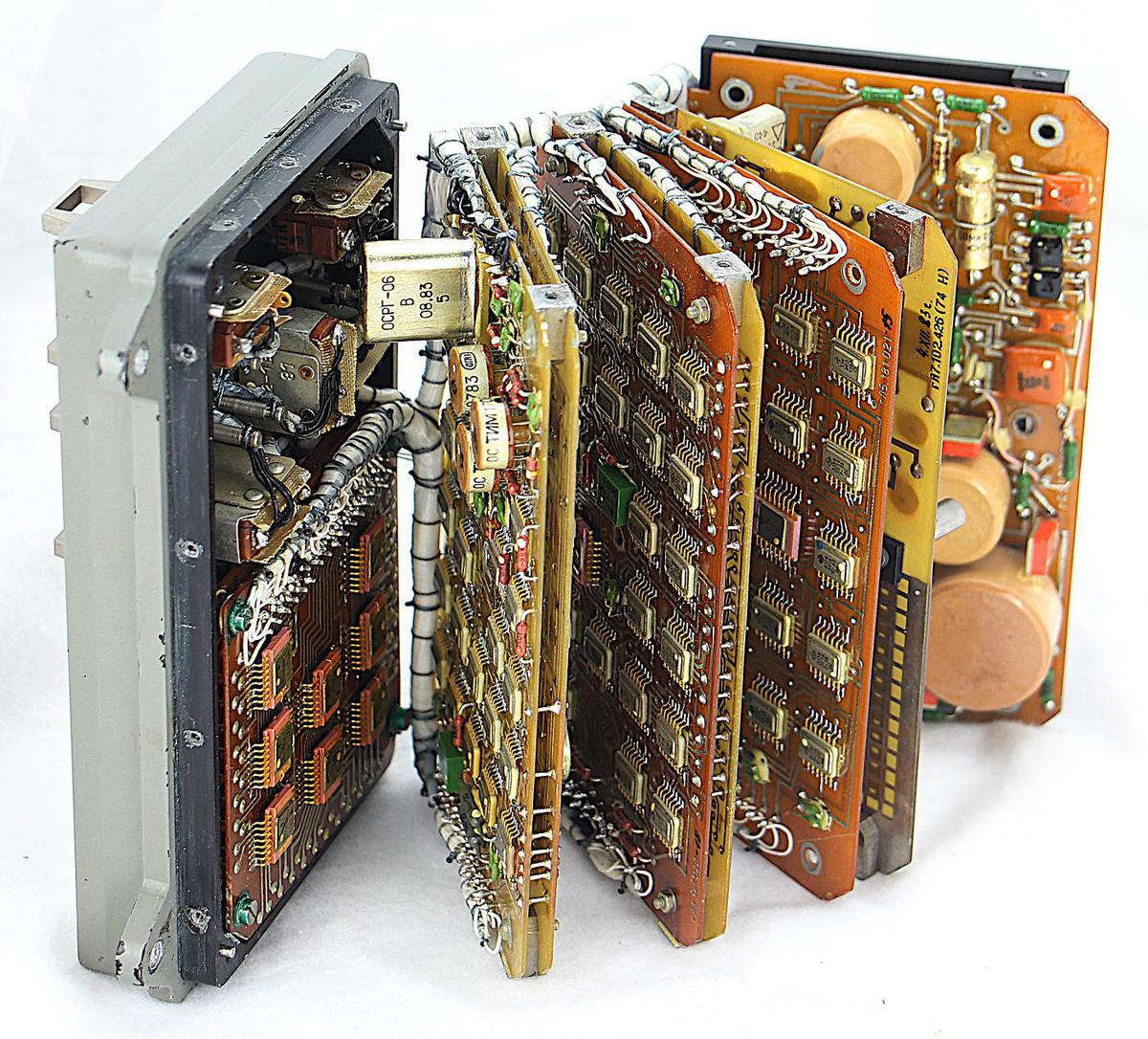
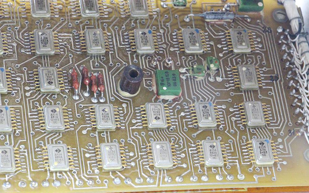
The clock's circuit boards can be opened like a book to reveal the integrated circuits and other components, thanks to the flexible wiring harnesses that connect the boards. The integrated circuits are mostly 14-pin "flat packs" in metal packages, surface-mounted on the printed circuit boards. I wanted to know more about these integrated circuits, so I opened one up,2 took photos, and reverse-engineered the chip's circuitry.

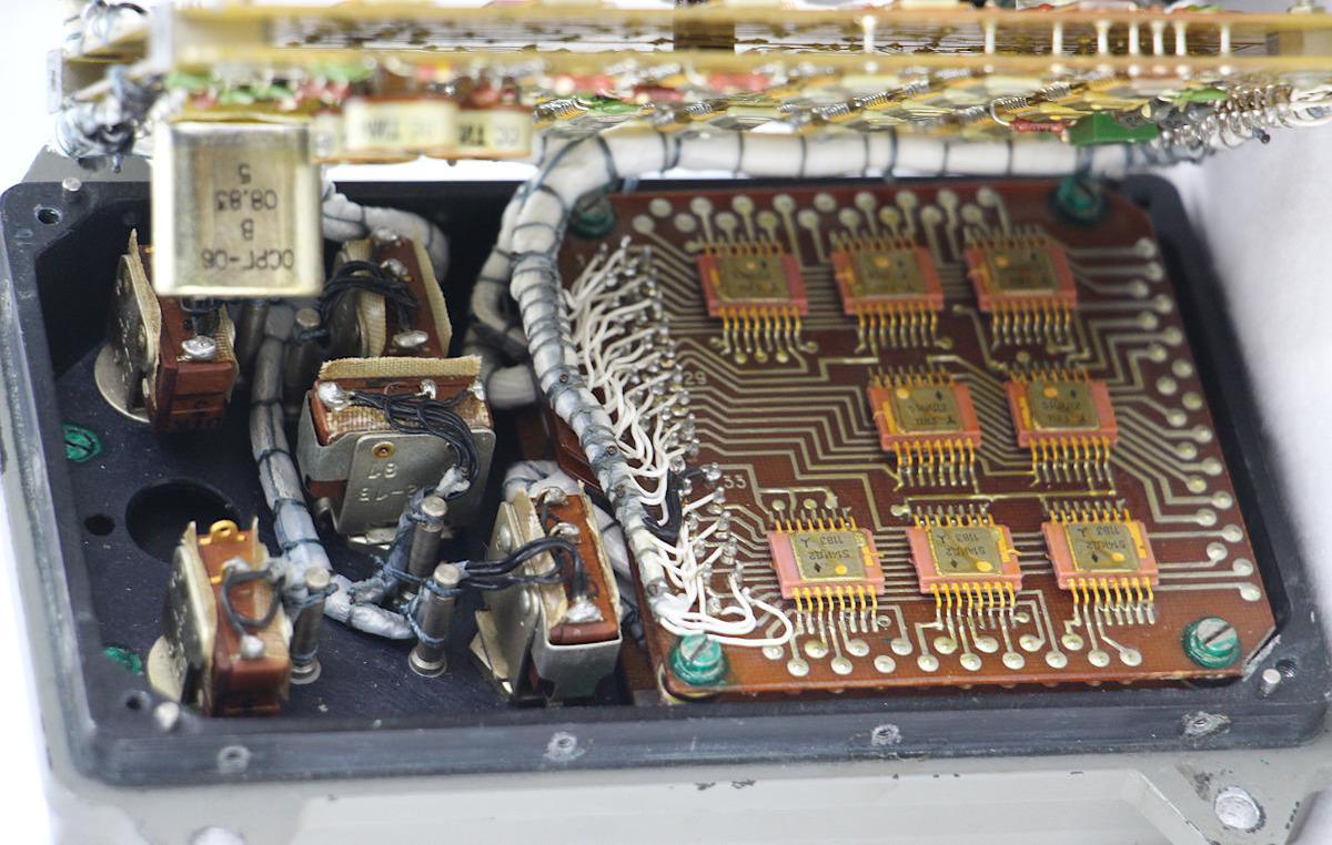
The wiring bundles are arranged so the boards can swing apart. The quartz crystal that controls the clock's timing is visible in the upper center. The clock's power supply is on the boards at the right, with multiple round inductors.

The wiring bundles are arranged so the boards can swing apart. The quartz crystal that controls the clock's timing is visible in the upper center. The clock's power supply is on the boards at the right, with multiple round inductors.

Soviet integrated circuits

The clock is built from TTL integrated circuits, a type of digital logic that was popular in the 1970s through the 1990s because it was reliable, inexpensive, and easy to use. (If you've done hobbyist digital electronics, you probably know the 7400-series of TTL chips.) A basic TTL chip contained just a few logic gates, such as 4 NAND gates or 6 inverters, while a more complex TTL chip implemented a functional unit such as a 4-bit counter. Eventually, TTL lost out to CMOS chips (the chips in modern computers), which use much less power and are much denser.

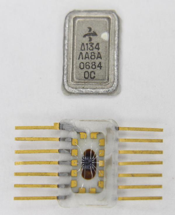
The photo below shows a chip with its metal lid removed. The tiny silicon die is visible in the middle, with bond wires connecting the die to the pins. This integrated circuit is very small; the ceramic package is 9.5mm×6.5mm, considerably smaller than a fingernail. To open up a chip like this, I normally put it in a vise and then tap the seam with a chisel. However, in this case, the chip decapped itself—while I was looking for a hammer, the top suddenly popped off due to the pressure from the vise.

The integrated circuit with its metal lid removed, showing the tiny silicon die inside.

The integrated circuit with its metal lid removed, showing the tiny silicon die inside.

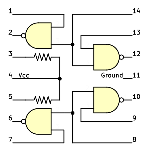
The chip I'm examining has the Cyrillic part number 134ЛА8 (134LA8)6. It implements four open-collector NAND gates, as shown below.4 The NAND gate is a standard logic gate, outputting a 0 if both inputs are 1, and otherwise outputting a 1. An open-collector output is slightly different from a standard output. It will pull the output pin low for a 0, but for a 1 it just leaves the output floating ("high impedance").5 An external pull-up resistor is required to pull the output high for a 1. The clock uses three of these chips: one in the quartz crystal oscillator circuit, and another functioning as inverters in another part of the clock.3

Logic diagram of the Soviet 134ЛА8 (134LA8) integrated circuit, with pin numbers.

Logic diagram of the Soviet 134ЛА8 (134LA8) integrated circuit, with pin numbers.

The Soviet Union lagged about 9 years behind the US in integrated circuit development.7 The lag would have been much larger, except the Soviet Union copied many Western integrated circuits. As a result, most of the Soviet TTL chips have Western equivalents.4 However, the 134ЛА8 chip that I examined is different from Western chips8 with two unusual features. First, to reduce the number of external resistors, this chip includes two pull-up resistors on the chip that can be wired up as desired. Second, the chip shares two NAND gate inputs, which frees up the two pins used by the resistors. Thus, even though the Soviet Union was copying integrated circuits, they were also creatively designing their own chips.

Integrated circuit components

Under the microscope, the transistors and resistors of the integrated circuit are visible. The silicon die appears in shades of pink, purple, and green, depending on how different regions of the chip have been "doped". By doping the silicon with impurities, the silicon takes on different semiconductor properties, making N-type and P-type silicon. On top of the silicon, the white lines are metal traces that wire together the components on the silicon layer.

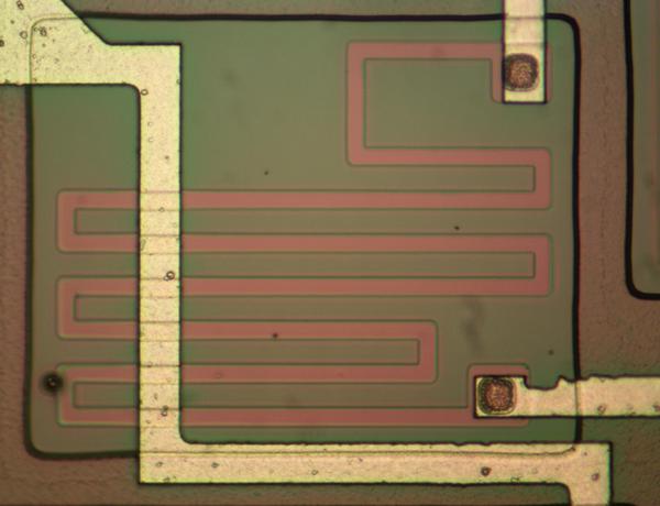
The photo below shows how a resistor appears on the silicon die. A resistor is formed by doping silicon to form a high-resistance path, the reddish line below. The longer the path, the higher the resistance, so the resistors typically zig-zag back and forth to create the desired resistance. The resistor is connected to the metal layer at both ends, while another metal passes over the resistor shown below.

A resistor on the integrated circuit die.

A resistor on the integrated circuit die.

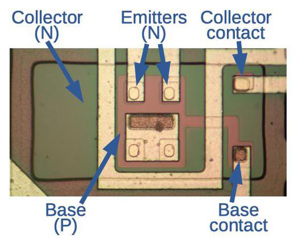
This chip, like other TTL chips, uses bipolar NPN transistors. These transistors have N-type silicon for the emitter, P-type silicon for the base, and N-type silicon for the collector. On the IC, the transistors are constructed by doping the silicon to form layers with different properties. At the bottom of the stack, the collector forms the bulk of the transistor, doped to form N-type silicon (the large green area below). On top of the collector, a thin region of P-type silicon forms the base; this is the reddish region in the middle. Finally, a small square N-type emitter is formed on top of the base. These layers form the N-P-N structure of the transistor. Note that the metal wiring to the collector and base is off to the side, away from the main body of the transistor.

An input transistor on the integrated circuit die. The transistor is surrounded by an isolation ring (dark color) to separate it from the other transistors.

An input transistor on the integrated circuit die. The transistor is surrounded by an isolation ring (dark color) to separate it from the other transistors.

TTL circuits typically used transistors with multiple emitters, one for each input, and this can be seen above. A multiple-emitter transistor may seem strange, but it is straightforward to build one on an integrated circuit. The transistor above has two emitters wired up. Close examination shows there are four emitters, but the two lower unused emitters are shorted to the base.

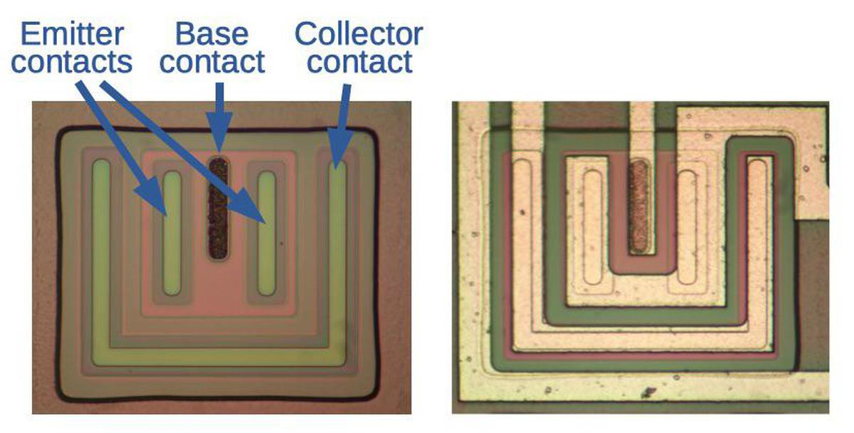
The output transistors on the chip produce the external signal from the chip, so they must support much higher current than the other transistors. As a result, they are much larger than the other transistors. As before, the transistor has a large N-type collector region (green), with a base on top (pink), and then emitter on top of the base. The output transistor has long contacts between the metal layer and the silicon, rather than the small square contacts of the previous transistor. The emitter (wired in a "U" shape) is also much larger. These changes allow more current to flow through the transistor. In the photo below, the transistor on the left has no metal layer, so its silicon features are more visible.9 The transistor on the right shows the metal wiring.

Two output transistors on the integrated circuit die. The one on the left is unused, while the one on the right is wired into the circuit by the metal layer.

Two output transistors on the integrated circuit die. The one on the left is unused, while the one on the right is wired into the circuit by the metal layer.

How a TTL NAND gate works

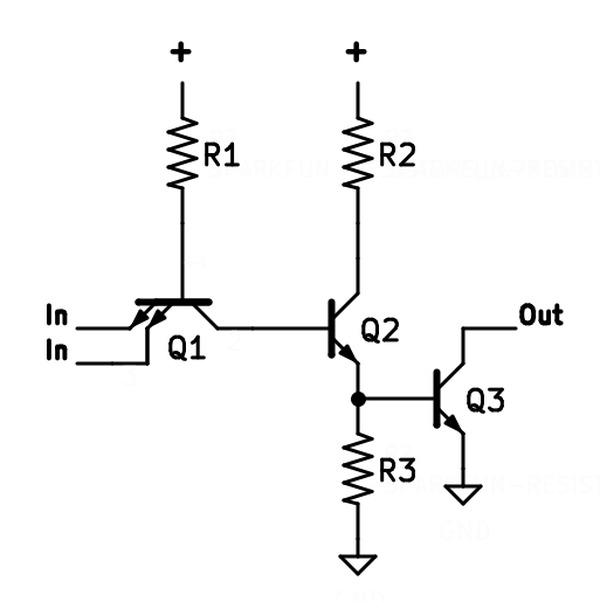
The schematic below shows one of the open-collector NAND gates in the chip. In this paragraph, I'll give a brief explanation of the circuit; you can skip this if you want.10 To understand the circuit, first assume that an input is 0. The current through resistor R1 and the base of transistor Q1 will flow out through the transistor's emitter and the low input. Transistor Q2 will be off, so R3 pulls Q3's base low, turning Q3 off. Thus, the output will float (i.e. open-collector 1 output). On the other hand, suppose both inputs are 1. Now the current through R1 can't pass through an input so it will flow out the collector of Q1 (i.e. backward) and into Q2's base, turning on Q2. Q2 will pull Q3's base high, turning on Q3 and pulling the output low. Thus, the circuit implements a NAND gate, outputting 0 if both inputs are high. Note that Q1 isn't acting like a normal transistor, but instead is "current-steering", directing the current from R1 in one direction or the other.

Schematic of one gate in the integrated circuit. This is an open-collector TTL NAND gate.

Schematic of one gate in the integrated circuit. This is an open-collector TTL NAND gate.

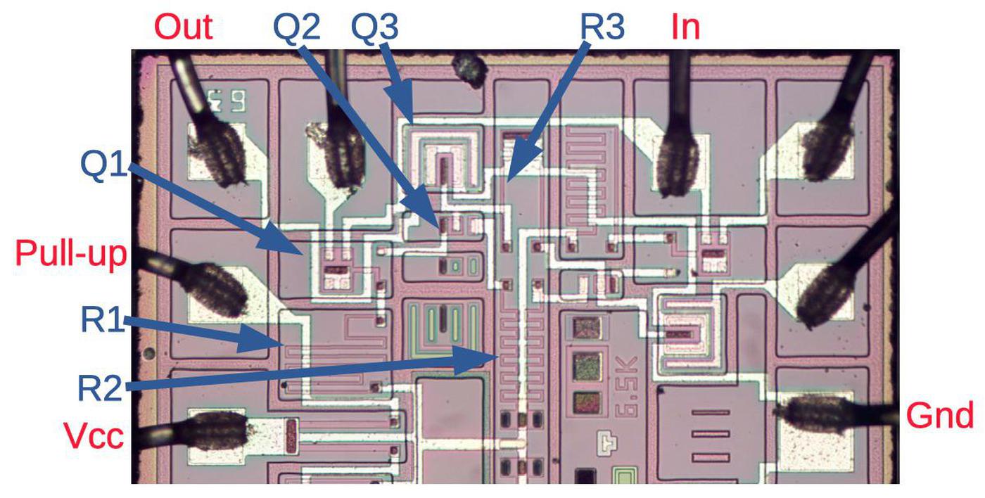
The diagram below shows the components for one of the NAND gates, labeled to match the schematic. (The three other NAND gates on the chip are similar.) The wiring of the gate is simple compared to most integrated circuits; you can follow the metal traces (white) and match up the wiring with the schematic. Note the winding path from the ground pad to Q3. Q1 is a two-emitter transistor while Q3 is a large output transistor. Two unused transistors are below Q2.

The die, showing the components in a gate. Components are labeled (blue) for one of the NAND gates, while pins are labeled in red. The pull-up resistors are above and below the Vcc wire.

The die, showing the components in a gate. Components are labeled (blue) for one of the NAND gates, while pins are labeled in red. The pull-up resistors are above and below the Vcc wire.

Conclusion

This Soviet chip from 1984 is simple enough that the circuitry can be easily traced out, illustrating how a TTL NAND gate is constructed. The downside of simple chips, however, is that the Soyuz clock required over 100 chips to implement basic clock functionality. Even at the time, single chips implemented wristwatches and alarm clocks. Now, modern chips can contain billions of transistors, providing an extraordinary amount of functionality, but making the chip impossible to understand visually.

My previous blog post discussed the clock's circuitry in detail and I plan to write more about the clock, so follow me @kenshirriff (or on RSS) for details. Until then, you can watch CuriousMarc's video showing the disassembly of the space clock:

Notes and References

  1. CuriousMarc obtained the clock from an auction and it was advertised as flown to space, but we don't know which mission it was flown on. The date codes on the components inside the clock are mostly from 1983, with one from 1984, so the clock was probably manufactured in 1984. The Russian name for the clock is "Бортовые Часы Космические" (Onboard Space Clock), which is abbreviated as "БЧК". 

  2. Don't worry; I didn't destroy any of the chips in the clock. We bought duplicate chips on eBay for reverse-engineering. I was surprised that most of these 1980s-era chips are not too hard to obtain. 

  3. I don't see any obvious reason why the 134ЛА8 chip was used instead of an inverter chip. Surprisingly, even though the 7404 hex inverter chip was extremely common in US designs, the clock doesn't use any inverter chips at all. 

  4. For more information on Russian integrated circuits, including the ones used in the clock, see the databook Интегральные микросхемы и их зарубежные аналоги (Integrated circuits and their foreign counterparts). (The title makes it explicit that they were copying foreign chips.) Be warned that the databook's description of the 134ЛА8 has a few typos. 

  5. One reason to use open-collector gates is to get an AND gate "for free". Connecting outputs together produces a wired-AND; if any output is a 0, the tied-together output is a 0. (Tying together NAND gates is equivalent to AND-OR-INVERT logic.)

    Open-collector outputs can also be used on a bus, where multiple devices or boards can write signals to a bus line (as in the Xerox Alto) without electrical conflict. This use is obsolete, though; tri-state outputs provide much better performance. 

  6. One nice thing about Russian ICs is that the part numbers are assigned according to a rational system, unlike the essentially random numbering of American integrated circuits. Two letters in the part number indicate the function of the chip, such as a logic gate, counter, flip flop, or decoder. For example, consider the label "Δ134 ЛA8A". The series number, 134, indicates the chip is a low-power TTL chip. The "Л" (L) indicates a logic chip (Логические), with "A" indicating the NAND gate subcategory. Finally, "8" indicates a specific type of NAND chip in the ЛA category. As with American chips, the "0684" date code on the chip indicates that it was made in the 6th week of 1984. 

  7. Two CIA reports (1974 and 1986) provide information on the lag between Soviet IC technology and Western technology. "Microcomputing in the Soviet Union and Eastern Europe", ABACUS, 1985, discusses how the Soviet Union copied American microprocessors, especially Intel ones. 

  8. The 7400 series includes several quad open-collector NAND gate chips, such as the 7401, 7403, 7426, 7438, and 7439. These are all different from the Soviet chip. A die photo of the 74S01 is here; I think the Soviet chip has a much nicer layout. 

  9. The integrated circuit has a few unused transistors. In addition, the input transistors have 4 emitters, but only two of them are used. This is probably so the same silicon die can be used to manufacture multiple integrated circuits by changing the metal layer. For instance, the 4-emitter transistors could be used for 3- or 4-input NAND gates. Alternatively, the unused transistors could be used to create a hex inverter chip. 

  10. For a detailed explanation of how TTL gates work, see this page

The core memory inside a Saturn V rocket's computer

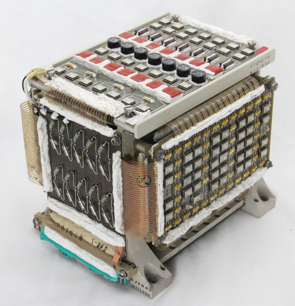
The Launch Vehicle Digital Computer (LVDC) had a key role in the Apollo Moon mission, guiding and controlling the Saturn V rocket. Like most computers of the era, it used core memory, storing data in tiny magnetic cores. In this article, I take a close look at an LVDC core memory module from Steve Jurvetson's collection. This memory module was technologically advanced for the mid-1960s, using surface-mount components, hybrid modules, and flexible connectors that made it an order of magnitude smaller and lighter than mainframe core memories.2 Even so, this memory stored just 4096 words of 26 bits.1

A core memory module from the LVDC. This module stored 4K words of 26 data bits and 2 parity bits. It weighs 2.3 kg (5.1 pounds) and measures about 14 cm×14 cm×16 cm (5½"×5½"×6"). Click on any photo for a larger version.

A core memory module from the LVDC. This module stored 4K words of 26 data bits and 2 parity bits. It weighs 2.3 kg (5.1 pounds) and measures about 14 cm×14 cm×16 cm (5½"×5½"×6"). Click on any photo for a larger version.

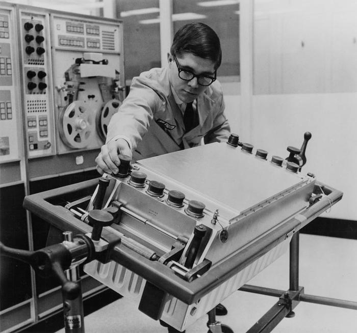
The race to the Moon started on May 25, 1961 when President Kennedy stated that America would land a man on the Moon before the end of the decade. This mission required the three-stage Saturn V rocket, the most powerful rocket ever built. The Saturn V was guided and controlled by the Launch Vehicle Digital Computer3 (below), from liftoff into Earth orbit, and then on a trajectory towards the Moon. (The Apollo spacecraft separated from the Saturn V rocket at that point, ending the LVDC's role.)

The LVDC mounted in a support frame. The round connectors are visible on the front side of the computer. There are 8 electrical connectors and two connectors for liquid cooling. Photo courtesy of IBM.

The LVDC mounted in a support frame. The round connectors are visible on the front side of the computer. There are 8 electrical connectors and two connectors for liquid cooling. Photo courtesy of IBM.

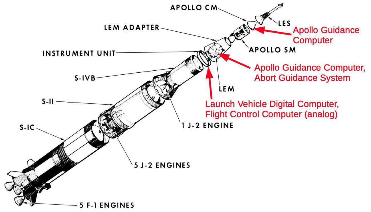
The LVDC was just one of several computers onboard the Apollo mission. The LVDC was connected to the Flight Control Computer, a 100-pound analog computer. The Apollo Guidance Computer (AGC) guided the spacecraft to the Moon's surface. The Command Module contained one AGC while the Lunar Module contained a second AGC7 along with the Abort Guidance System, an emergency backup computer.

Multiple computers were onboard an Apollo mission. The Launch Vehicle Digital Computer (LVDC) is the one discussed in this blog post.

Multiple computers were onboard an Apollo mission. The Launch Vehicle Digital Computer (LVDC) is the one discussed in this blog post.

Unit Logic Devices (ULD)

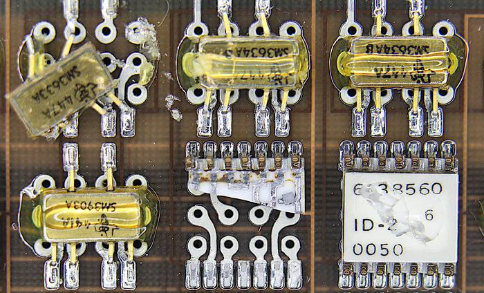
The LVDC was built with an interesting hybrid technology called ULD (Unit Logic Devices). Although they superficially resembled integrated circuits, ULD modules contained multiple components. They used simple silicon dies, each implementing just one transistor or two diodes. These dies, along with thick-film printed resistors, were mounted on a half-inch-square ceramic wafer to implement a circuit such as a logic gate. These modules were a variant of the SLT (Solid Logic Technology) modules developed for IBM's popular S/360 series of computers. IBM started developing SLT modules in 1961, before integrated circuits were commercially viable, and by 1966 IBM produced over 100 million SLT modules a year.

ULD modules were considerably smaller than SLT modules, as shown in the photo below, making them more suitable for a compact space computer.4 ULD modules used ceramic packages instead of SLT's metal cans, and had metal contacts on the upper surface instead of pins. Clips on the circuit board held the ULD module in place and connected with these contacts.5 The LVDC and associated hardware used more than 50 different types of ULDs.

SLT modules (left) are considerably larger than ULD modules (right). A ULD module is 7.6 mm × 8 mm.

SLT modules (left) are considerably larger than ULD modules (right). A ULD module is 7.6 mm × 8 mm.

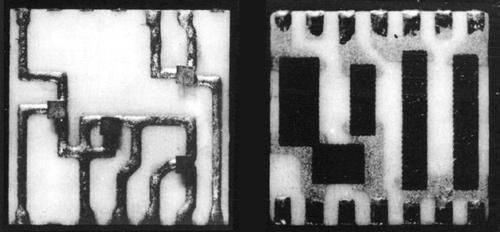
The photo below shows the internal components of a ULD module. On the left, the circuit traces are visible on the ceramic wafer, connected to four tiny square silicon dies. While this looks like a printed circuit board, keep in mind that it is much smaller than a fingernail. On the right, the black rectangles are thick-film resistors printed onto the underside of the wafer.

Top and underside of a ULD showing the silicon dies and resistors. While SLT modules had resistors on the upper surface, ULD modules had resistors underneath, increasing the density but also the cost. From IBM Study Report Figure III-11.

Top and underside of a ULD showing the silicon dies and resistors. While SLT modules had resistors on the upper surface, ULD modules had resistors underneath, increasing the density but also the cost. From IBM Study Report Figure III-11.

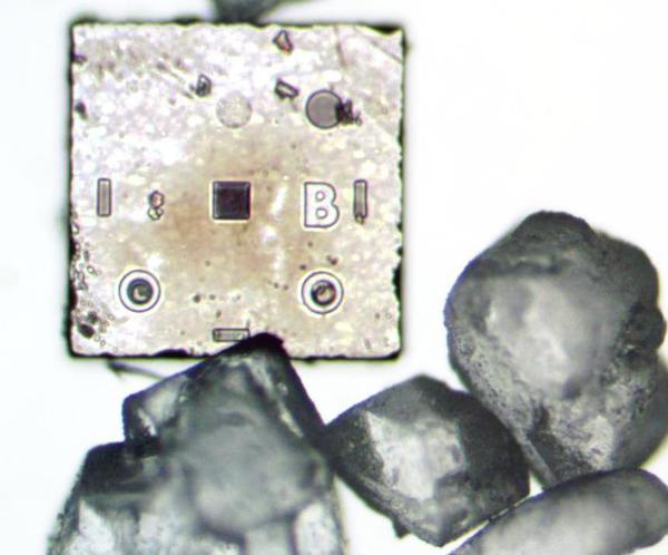
The microscope photo below shows a silicon die from a ULD module that implements two diodes.6 The die is very small; for comparison, grains of sugar are displayed next to the die. The die had three external connections through copper balls soldered to the three circles. The two lower circles were doped (darker regions) to form the anodes of the two diodes, while the upper-right circle was the cathode, connected to the substrate. Note that this die is much less complex than even a basic integrated circuit.

Photo of a two-diode silicon die next to sugar crystals. This photo is a composite of top-lighting to show the die details, with back-lighting to show the sugar.

Photo of a two-diode silicon die next to sugar crystals. This photo is a composite of top-lighting to show the die details, with back-lighting to show the sugar.

How core memory works

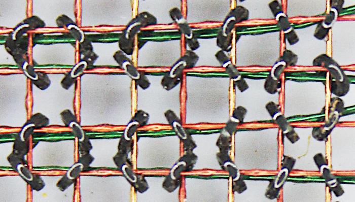
Core memory was the dominant form of computer storage from the 1950s until it was replaced by semiconductor memory chips in the 1970s. Core memory was built from tiny ferrite rings called cores, storing one bit in each core by magnetizing the core either clockwise or counterclockwise. A core was magnetized by sending a pulse of current through wires threaded through the core. The magnetization could be reversed by sending a pulse in the opposite direction.

To read the value of a core, a current pulse flipped the core to the 0 state. If the core was in the 1 state previously, the changing magnetic field created a voltage in a sense wire threaded through the cores. But if the core was already in the 0 state, the magnetic field wouldn't change and the sense wire wouldn't pick up a voltage. Thus, the value of the bit in the core was read by resetting the core to 0 and testing the sense wire. An important characteristic of core memory was that the process of reading a core destroyed its value, so it needed to be re-written.

Using a separate wire to flip each core would be impractical, but in the 1950s a technique called "coincident-current" was developed that used a grid of wires to select a core. This depended on a special property of cores called hysteresis: a small current has no effect on a core, but a current above a threshold would magnetize the core. This allowed a grid of X and Y lines to select one core from the grid. By energizing one X line and one Y line each with half the necessary current, only the core where both lines crossed would get enough current to flip leaving the other cores unaffected.

Closeup of an IBM 360 Model 50 core plane. The LVDC and Model 50 used the same type of cores, known as 19-32 because their
inner diameter was 19 mils and their outer diameter was 32 mils (0.8 mm).
While this photo shows three wires through each core, the LVDC used four wires.

Closeup of an IBM 360 Model 50 core plane. The LVDC and Model 50 used the same type of cores, known as 19-32 because their inner diameter was 19 mils and their outer diameter was 32 mils (0.8 mm). While this photo shows three wires through each core, the LVDC used four wires.

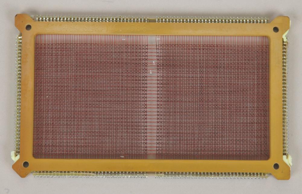
The photo below shows one core plane from the LVDC's memory.8 This plane has 128 X wires running vertically and 64 Y wires running horizontally, with a core at each intersection. For reading, a single sense wire runs through all the cores parallel to the Y wires. For writing, a single inhibit wire (explained below) runs through all the cores parallel to the X wires. The sense wires cross over in the middle of the plane; this reduces induced noise because noise from one half of the plane cancels out noise from the other half.

One core plane for the LVDC's memory, holding 8192 bits. Connections to the core plane are made through the pins around the outside. From Smithsonian National Air and Space Museum.

One core plane for the LVDC's memory, holding 8192 bits. Connections to the core plane are made through the pins around the outside. From Smithsonian National Air and Space Museum.

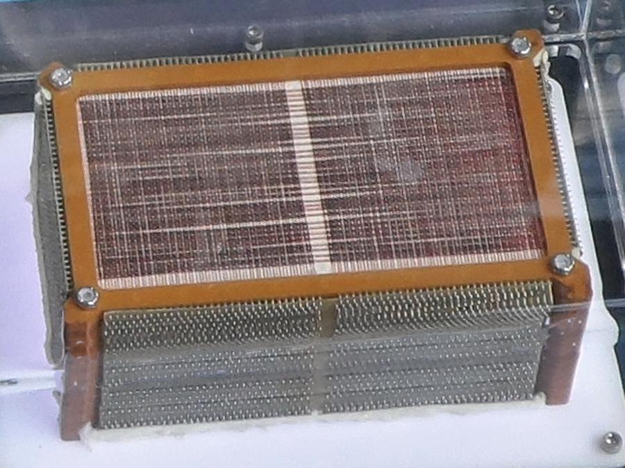
The plane above had 8192 locations, each storing a single bit. To store a word of memory, multiple core planes were stacked together, one plane for each bit in the word. The X and Y select lines were wired to zig-zag through all the core planes, in order to select a bit of the word from each plane. Each plane had a separate sense line for reading, and a separate inhibit line for writing. The LVDC memory used a stack of 14 core planes (below), storing a 13-bit "syllable" along with a parity bit.10

The LVDC core stack consists of 14 core planes. This stack is at the US Space & Rocket Center. Photo from NCAR EOL. I retouched the photo to reduce distortion from the plastic case.

The LVDC core stack consists of 14 core planes. This stack is at the US Space & Rocket Center. Photo from NCAR EOL. I retouched the photo to reduce distortion from the plastic case.

Writing to core memory required additional wires called the inhibit lines. Each plane had one inhibit line threaded through all the cores in the plane. In the write process, a current passed through the X and Y lines, flipping the selected cores (one per plane) to the 1 state, storing all 1's in the word. To write a 0 in a bit position, the plane's inhibit line was energized with half current, opposite to the X line. The currents canceled out, so the core in that plane would not flip to 1 but would remain 0. Thus, the inhibit line inhibited the core from flipping to 1. By activating the appropriate inhibit lines, any desired word could be written to the memory.

To summarize, a core memory plane had four wires through each core: X and Y drive lines, a sense line, and an inhibit line. These planes were stacked to form an array, one plane for each bit in the word. By energizing an X line and a Y line, one core in each plane was selected. The sense line was used to read the contents of the bit, while the inhibit line was used to write a 0 (by inhibiting the writing of a 1).9

The LVDC core memory module

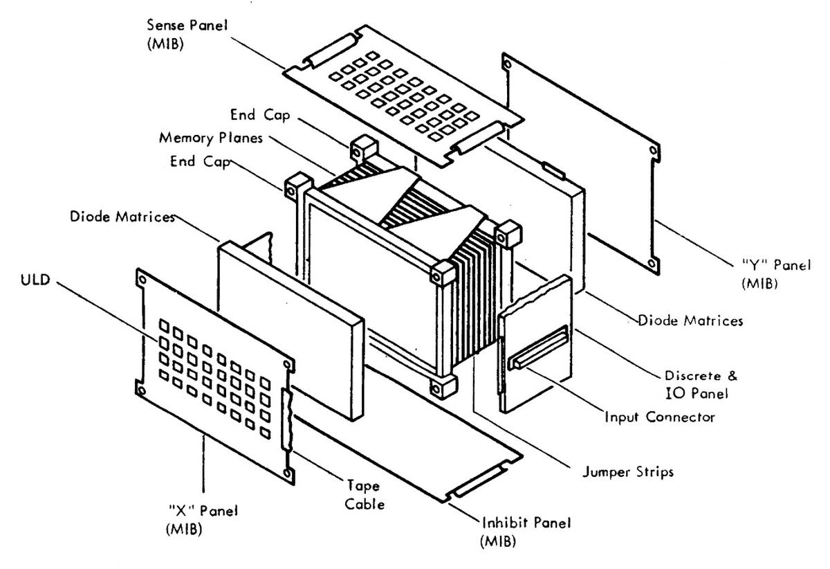
In this section, I'll explain how the LVDC core memory module was physically constructed. At its center, the core memory module contains the stack of 14 core planes shown earlier. This is surrounded by multiple boards with the circuitry to drive the X and Y select lines and the inhibit lines, read the bits from the sense lines, detect errors, and generate necessary clock signals.11

An exploded view of the memory module showing the key components.
An MIB (Multilayer Interconnection Board) is a 12-layer printed circuit board.
From Saturn V Guidance Computer Progress Report Fig 2-43.

An exploded view of the memory module showing the key components. An MIB (Multilayer Interconnection Board) is a 12-layer printed circuit board. From Saturn V Guidance Computer Progress Report Fig 2-43.

Memory Y driver panel

A word in core memory is selected by driving the appropriate X and Y lines through the core stack. I'll start by describing the Y driver circuitry and how it generates a signal through one of the 64 Y lines. Instead of having 64 separate driver circuits, the module reduces the amount of circuitry by using 8 "high" drivers and 8 "low" drivers. These are wired up in a "matrix" configuration so each combination of a high driver and a low driver selects a different line. Thus, the 8 high drivers and 8 low drivers select one of the 64 (8×8) Y lines. The footnote12 has more information on the matrix technique.

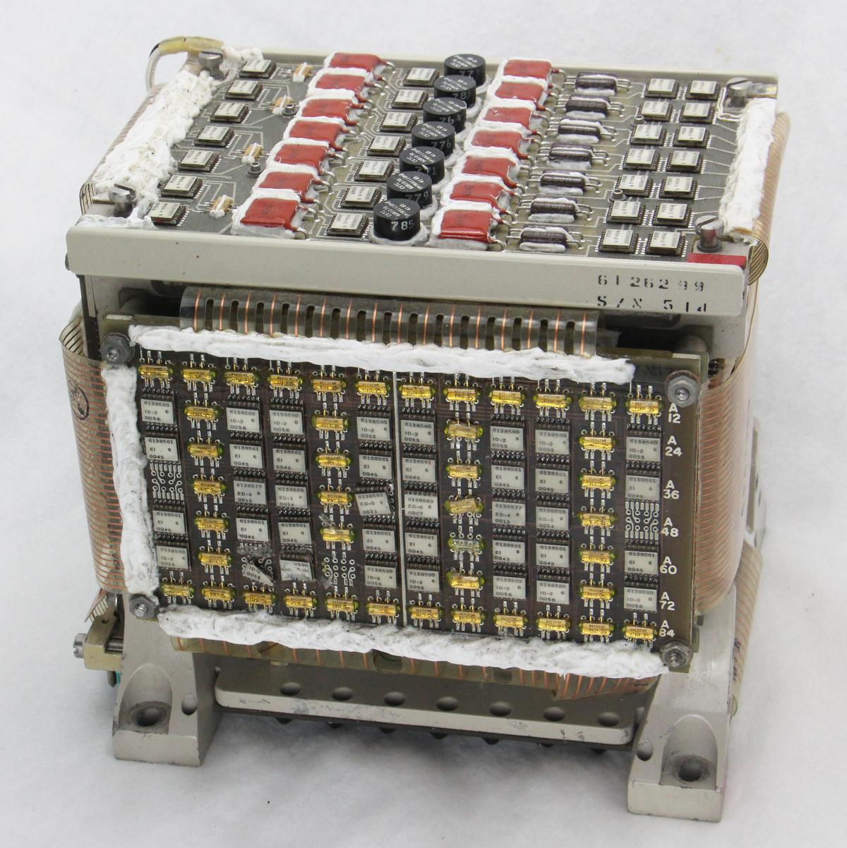
The Y driver board (front) drives the Y select lines in the core stack.

The Y driver board (front) drives the Y select lines in the core stack.

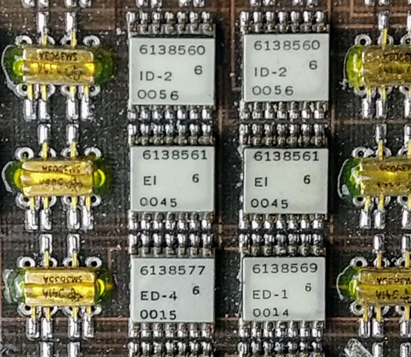
The closeup view below shows some of the ULD modules (white) and transistor pairs (golden) that drive the Y select lines. The "EI" module is the heart of the driver; it supplies a constant voltage pulse (E) or sinks a constant current pulse (I) through a select line.14 A select line is driven by activating an EI module in voltage mode at one end of the line and an EI module in current mode at the other end. The result is a pulse with the correct voltage and current to flip the core. It takes a hefty pulse to flip a core; the voltage pulse is fixed at 17 volts, while the current is adjusted from 180 mA to 260 mA depending on the temperature.13

Closeup of the Y driver board showing six ULD modules and six transistor pairs. Each ULD module is labeled with an IBM part number, the module type (e.g. "EI"), and an unknown code.

Closeup of the Y driver board showing six ULD modules and six transistor pairs. Each ULD module is labeled with an IBM part number, the module type (e.g. "EI"), and an unknown code.

The board also has error-detector (ED) modules that detect if more than one Y select line is driven at the same time. Implementing this with digital logic would require a complicated set of gates to detect if two or more of the 8 inputs are high. Instead, the ED module uses a simple semi-analog design: it sums the input voltages using a resistor network. If the resulting voltage is above a threshold, the output is triggered.

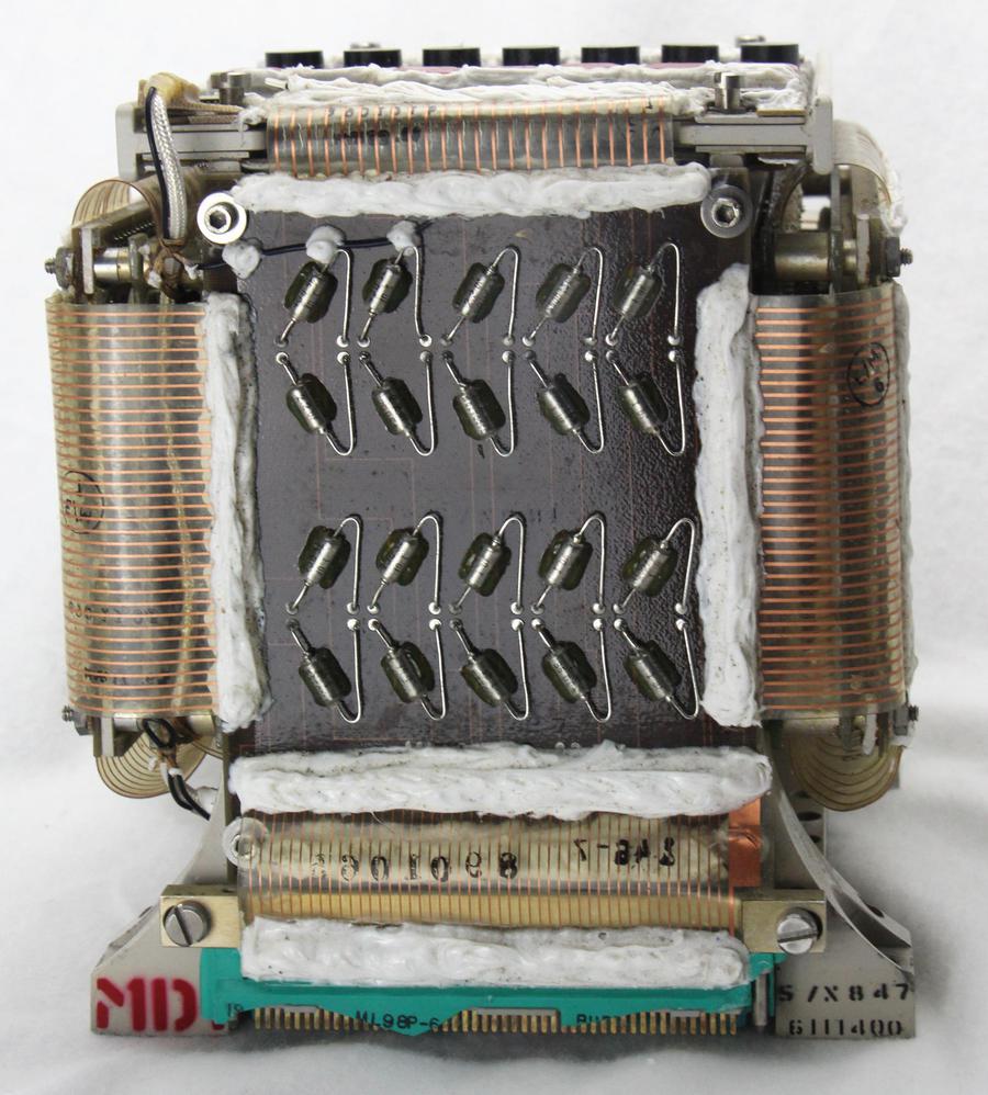
A diode matrix is underneath the driver board, containing 256 diodes and 64 resistors. This matrix converts the 8 high and 8 low pairs of signals from the driver board into connections to the 64 Y lines that pass through the core stack. Flex cables on the top and bottom of the board connect the board to the diode matrix. Two flex cables on the left (not visible in the photo) and two flex cables on the right (one visible) connect the diode matrix to the core stack.15 The flex cable visible on the left connects the Y board to the rest of the computer via the I/O board (described later) while a small flex cable on the lower right connects to the clock board.

Memory X driver panel

The circuitry to drive the X lines is similar to the Y circuitry, except there are 128 X lines compared to 64 Y lines. Because there are twice as many X lines, the module has a second X driver board underneath the one visible below. Although the X and Y boards have the same components, the wiring is different.

This board and the similar one underneath drive the X select lines in the core stack.

This board and the similar one underneath drive the X select lines in the core stack.

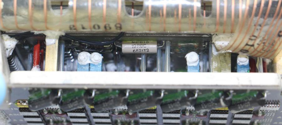
The closeup below shows that the board has suffered some component damage. One of the transistors has been dislodged, a ULD module has been broken in half, and the other ULD module is cracked. The wiring is visible inside the broken module as well as one of the tiny silicon dies (on the right). This photo also shows vertical and horizontal circuit board traces on several of the board's 12 layers.

A closeup of the X driver board showing some damaged circuitry.

A closeup of the X driver board showing some damaged circuitry.

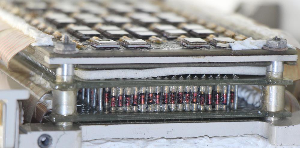
Underneath the X driver boards is the X diode matrix, containing 288 diodes and 128 resistors. The X diode matrix uses a different topology than the Y diode board to avoid doubling the number of components.16 Like the Y diode board, this board contains components mounted vertically between two printed circuit boards. This technique is called "cordwood" and allows the components to be packed together closely.

Closeup of X diode matrix showing diodes mounted vertically using cordwood construction between two printed circuit boards. The two X driver boards are above the diode board, separated from it by foam. Note how the circuit boards are packed very closely together.

Closeup of X diode matrix showing diodes mounted vertically using cordwood construction between two printed circuit boards. The two X driver boards are above the diode board, separated from it by foam. Note how the circuit boards are packed very closely together.

Memory sense amplifiers

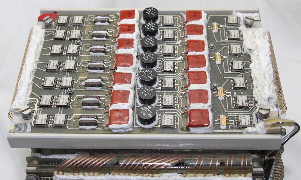
The photo below shows the sense amplifier board on top of the module.17 It has 7 channels to read 7 bits from the memory stack; an identical board below processes another 7 bits, for 14 bits in total. The job of the sense amplifier is to detect the small signal (20 millivolts) generated by a flipping core, and turn it into a 1-bit output. Each channel consists of a differential amplifier and buffer, followed by a differential transformer and an output latch. At the left, the 28-conductor flex cable connects to the memory stack, feeding the two ends of each sense wire into the amplifier circuitry, starting with an MSA-1 (Memory Sense Amplifier) module. The discrete components are resistors (brown cylinders), capacitors (red), transformers (black), and transistors (golden). The data bits exit the sense amplifier boards through the flex cable on the right.

The sense amplifier board on top of the memory module. This board amplifies the signals from the sense wires to produce the output bits.

The sense amplifier board on top of the memory module. This board amplifies the signals from the sense wires to produce the output bits.

Memory inhibit drivers

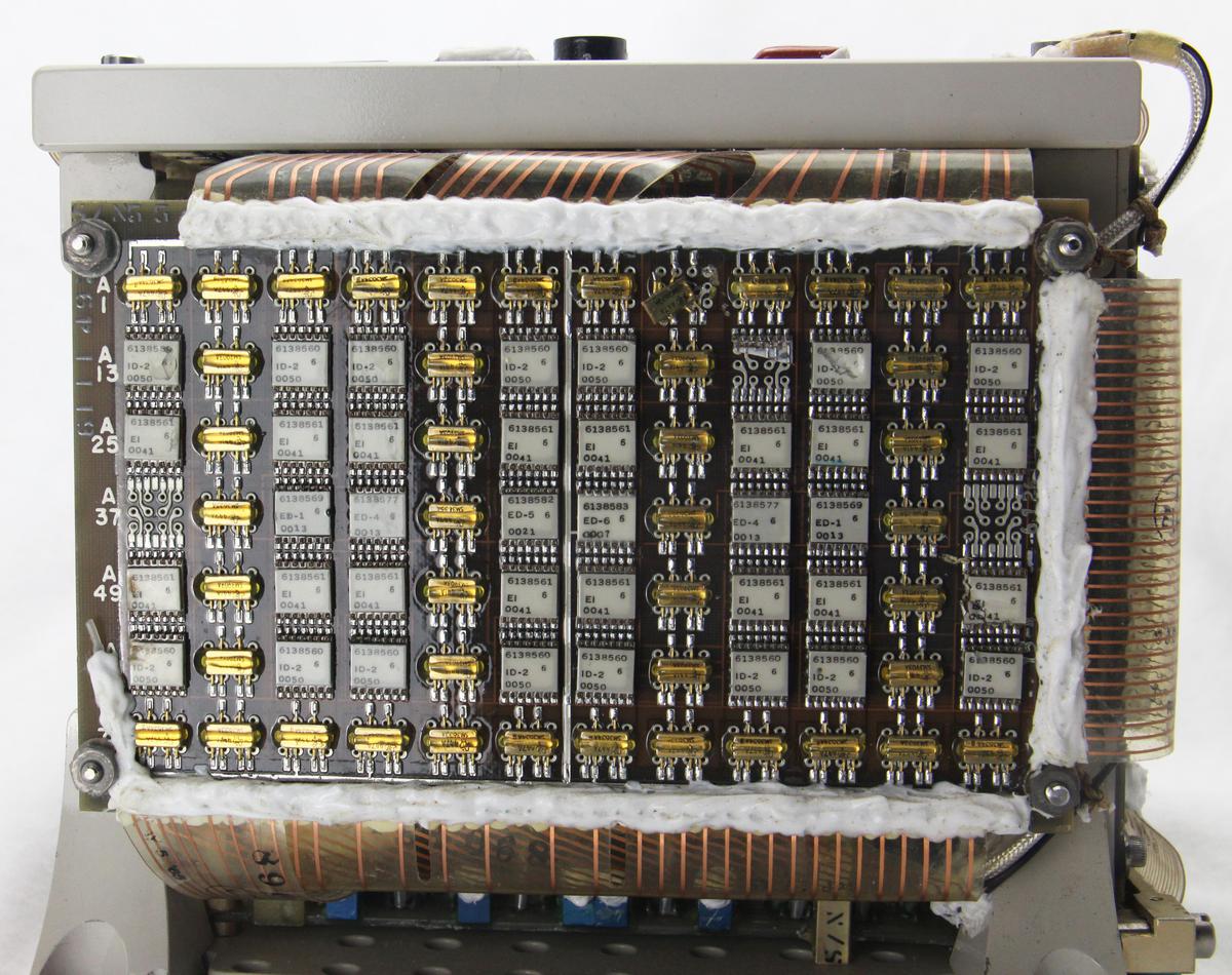
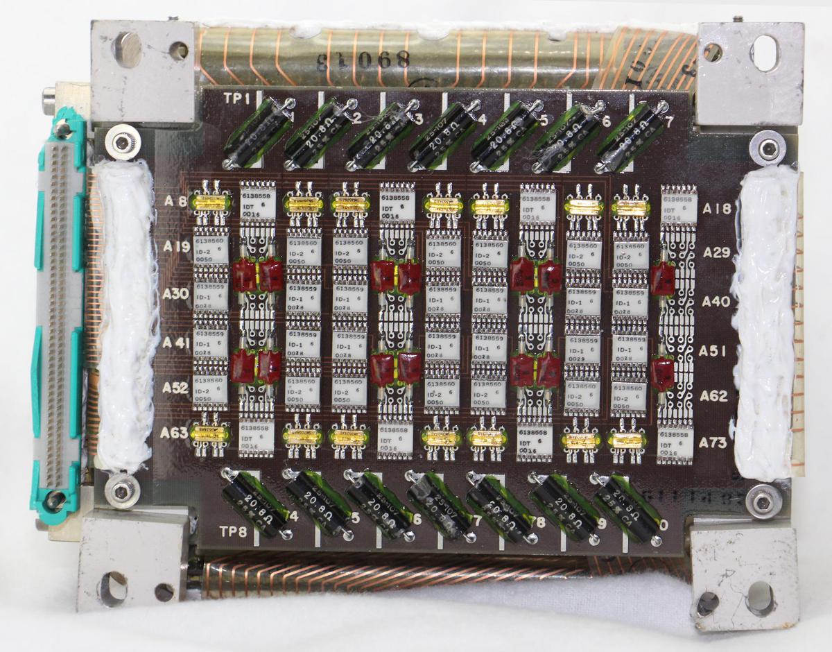
The inhibit board is on the underside of the core module and holds the inhibit drivers that are used for writing to memory. There are 14 inhibit lines, one for each plane in the core stack. To write a 0 bit, the corresponding inhibit driver is activated and the current through the inhibit line prevents the core from flipping to a 1. Each line is driven by an ID-1 and ID-2 (Inhibit Driver) module and a pair of transistors. The high-precision 20.8Ω resistors at the top and bottom of the board regulate the inhibit current. The 14-wire flex cable on the right connects the drivers to the 14 inhibit wires in the core stack.

The inhibit board on the bottom of the memory module. This board generates the 14 inhibit signals used during writing.

The inhibit board on the bottom of the memory module. This board generates the 14 inhibit signals used during writing.

Memory clock driver

The clock driver is a pair of boards that generate the timing signals for the memory module. Once the computer starts a memory operation, the various timing signals used by the memory module are generated asynchronously by the module's clock driver. The clock driver boards are on the bottom of the module, between the core stack and the inhibit board so it is hard to see the boards.

The clock driver boards are below the core memory stack but above the inhibit board.

The clock driver boards are below the core memory stack but above the inhibit board.

The photo above looks between the clock driver boards; the inhibit board is on the bottom. The blue components are multi-turn potentiometers, presumably to adjust timings or voltages. Resistors and capacitors are also visible on the boards. The schematic shows several MCD (Memory Clock Driver) modules, but I can't see any modules on the boards. I don't know if that is due to the limited visibility, a change in the circuitry, or another board with these modules.

Memory input-output panel

The final board of the memory module is the input-output panel (below), which distributes signals between the boards of the memory module and the remainder of the LVDC computer. At the bottom, the green 98-pin connector plugs into the LVDC's memory chassis, providing signals and power from the computer. (Much of the connector's plastic is broken, exposing the pins.) The distribution board is linked to this connector by two 49-pin flex cables at the bottom (only the front cable is visible). Other flex cables distribute signals to the X-driver board (left), the Y-driver board (right), the sense amplifier board (top), and inhibit board (underneath). The 20 capacitors on the board filter the power supplied to the memory module.

The input-output board is the interface between the memory module and the rest of the computer. The green connector at the bottom plugs into the computer, and these signals are routed through flat cables to other parts of the memory module. This board also has filter capacitors.

The input-output board is the interface between the memory module and the rest of the computer. The green connector at the bottom plugs into the computer, and these signals are routed through flat cables to other parts of the memory module. This board also has filter capacitors.

Conclusion

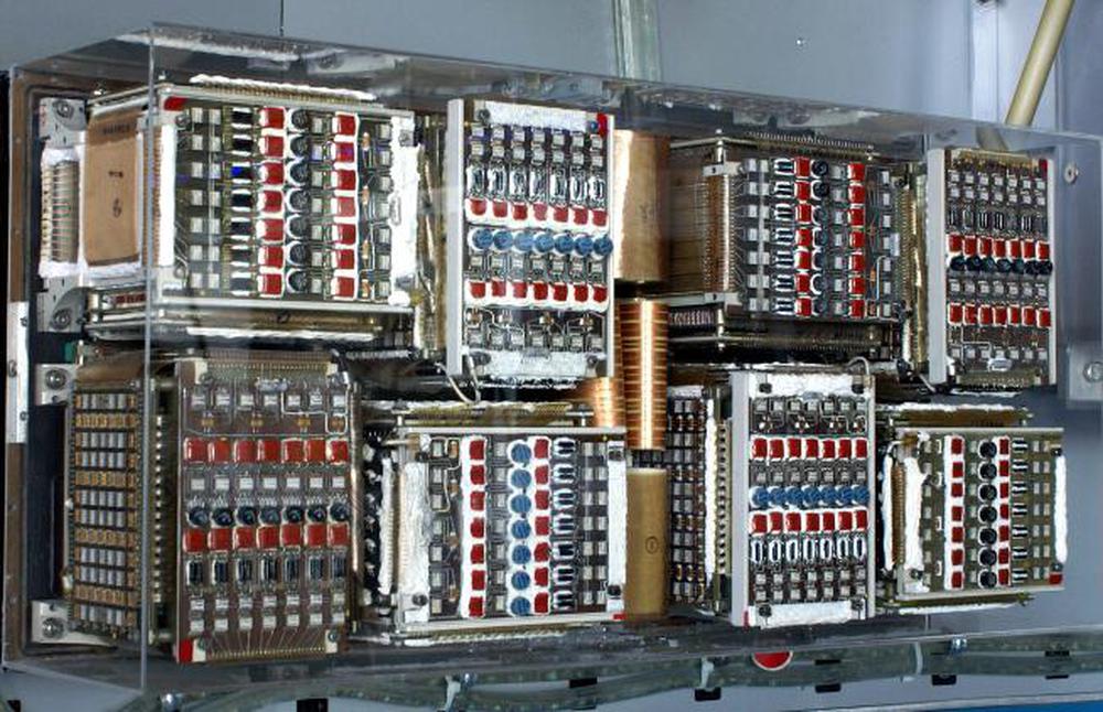
The LVDC's core memory module provided compact, reliable storage for the computer. The lower half of the computer (below) was filled by up to 8 core memory modules. This allowed the computer to hold a total of 32 kilowords of 26-bit words, or 16 kilowords in redundant high-reliability "duplex" mode.18

The LVDC held up to eight core memory modules. Photo at US Space & Rocket Center, courtesy of Mark Wells.

The LVDC held up to eight core memory modules. Photo at US Space & Rocket Center, courtesy of Mark Wells.

The core memory module provides an interesting view of a time when 8K of storage required a 5-pound module. While this core memory was technologically advanced for its time, the hybrid ULD modules were rapidly obsoleted by integrated circuits. Core memory as a whole died out in the 1970s with the advent of semiconductor DRAMs.

The contents of core memory are retained when the power is disconnected, so it's likely that the module still holds the software from when the computer was last used, even decades later. It would be interesting to try to recover this data, but the damaged circuitry poses a problem so the contents will probably remain locked inside the memory module for decades more.

I announce my latest blog posts on Twitter, so follow me @kenshirriff for future articles. I also have an RSS feed. For an explanation of core memory, see CuriousMarc's video where we wire up a core plane and demonstrate how it works. I've written before about core memory in the IBM 1401, core memory in the Apollo Guidance Computer, and core memory in the IBM S/360. Thanks to Steve Jurvetson for supplying the core array.

Notes and references

  1. A word size of 26 bits may seem bizarre, but in the 1960s computers hadn't yet standardized on bytes and word sizes that were a power of two. Business computers often used 6-bit characters, while aerospace computers typically used whatever word size provided the necessary accuracy. 

  2. It's interesting to compare the size of the LVDC's core memory to IBM's commercial core memories, which I wrote about here. The 128-kilobyte expansion for the IBM S/360 Model 40 computer required an additional cabinet weighing 610 pounds and measuring 62.5"×26"×60". An LVDC core memory module holds 4K words of 26 bits, equivalent to 13 kilobytes. Doing the math, the LVDC has 1/12 the weight and 1/40 the volume per byte. The core stack itself was very similar between the LVDC and the S/360 machines; the difference in weight and volume comes from the surrounding electronics and packaging. 

  3. For more information on the LVDC, see the Virtual AGC project's LVDC page. Also see the interesting SmarterEveryDay video on the LVDC. Fran Blanche did an extensive investigation into an LVDC circuit board. 

  4. The SLT modules in my photograph are mounted on an SMS card, rather than the expected SLT card. SMS cards were IBM's previous generation of circuit cards and normally used discrete germanium transistors. However, even after the introduction of SLT in 1964, IBM needed to support older computers with SMS cards. To reduce costs, they started building old-style SMS cards that used the more modern SLT modules. The point is that SLT modules were usually packed densely on multiple-layer circuit boards, rather than the low-density SMS card in the photo. 

  5. One question is why did IBM use SLT modules instead of integrated circuits? The main reason was that integrated circuits were still in their infancy, having been invented in 1959. In 1963, SLT modules had cost and performance advantages over integrated circuits. However, SLT modules were viewed outside IBM as backward compared to integrated circuits. One advantage of SLT modules over integrated circuits was that the resistors in SLT were much more accurate than those in integrated circuits. During manufacturing, the thick-film resistors in SLT modules were carefully sand-blasted to remove resistive film until they had the desired resistance. SLT modules were also cheaper than comparable integrated circuits in the 1960s. By 1969, IBM started using integrated circuits, which they called MST (Monolithic Systems Technology). IBM packaged their integrated circuits in SLT-style metal packages, rather than the industry-standard DIP epoxy packages. Chapter 2 of IBM's 360 and Early 370 Systems discusses the history of SLT modules in great detail. 

  6. Curiously, the ULD modules in the core memory did not contain any sealant inside. In contrast, the ULD modules examined by Fran Blanche were filled with pink silicone inside. 

  7. It's interesting to compare the AGC to the LVDC since they took two very different approaches to computer design and manufacture. Both computers had rectangular metal boxes, magnesium-lithium for the LVDC and magnesium for the AGC. Physically, the LVDC was about twice the size (2.2 cubic feet vs 1.1 cubic feet) even though they were both about 70 pounds. The LVDC used 138 Watts and was liquid-cooled, while the AGC used 55 watts and was cooled by conduction. The LVDC used 26-bit words compared to 15 bits in the AGC. One big architectural difference was that the LVDC was a serial computer, operating on one bit at a time, while the AGC operated on all bits in parallel (like most computers). Another important difference was that the LVDC used triple redundancy for reliability, while the AGC had no hardware fault handling. Both computers used a 2.048 MHz clock, but the LVDC was considerably slower because it was serial: 82 µs for an add operation compared to 23.4 µs for the AGC. The LVDC had up to 8 core memory modules, holding 4K words each. The AGC's core memory was only 2K words. However, the AGC also had 36K words of read-only storage in its hardwired core rope modules. (The LVDC did not use core rope.)

    The two computers were constructed in very different ways. The AGC was built from integrated circuits, while the LVDC used hybrid ULD modules. The AGC's logic gates were RTL (resistor-transistor logic) NOR gates, while the LVDC's were slightly more advanced DTL (diode-transistor logic) AND-OR-INVERT gates. While the AGC used two types of ICs (a dual NOR gate and a sense amplifier), the LVDC used many different types of modules.

    The AGC's circuit boards were encapsulated into rectangular modules, while the LVDC's circuit boards plugged into a backplane in a more standard way. The AGC's backplane was wire-wrapped by machine, while the LVDC's backplane was a 14-layer printed circuit board.

    IBM engaged in political battles, attempting to replace MIT's AGC with the LVDC. IBM argued that the AGC wasn't reliable enough compared to the triple-redundant LVDC. According to MIT, however, the AGC could run a guidance program 10 to 20 times faster than the LVDC, use half the memory, and provide more accuracy (by using double precision). MIT argued that the LVDC wasn't powerful enough to replace the AGC. In the end, the AGC survived the "naysayers" and was used on the Apollo spacecraft, while the LVDC had its role in the Saturn V rocket. The "showdown" is described in more detail here.  

  8. The Smithsonian website states that the core plane is approximately 4"×7"×1", but that can't be right since the entire memory module is less than 7" wide. The Study Report page 3-43 says each plane is 5.5"×3.5×0.15", which seems accurate. 

  9. The book Memories That Shaped an Industry discusses the history of core memory at IBM. 

  10. The LVDC has 26-bit words, each word consisting of two 13-bit syllables. Its core memory is described as holding 4K words, where each word is 26 data bits and 2 parity bits. However, the core memory is physically constructed to store 8K syllables (13 data bits and 1 parity bit). Thus, two memory accesses are required to read a complete word. An instruction is one 13-bit syllable so an instruction can be read in a single memory cycle. Thus, executing a typical instruction requires three memory accesses: one for the instruction and two for the data. (Keep in mind that reading from core memory erases the data, so a memory access consists of a read followed by a write to restore the data.) 

  11. Much of the memory-related circuitry is in the LVDC's computer logic, not the memory module itself. In particular, the computer's logic contains registers to hold the address and data word and convert between serial and parallel. It also contains circuitry to decode the address into drive lines, as well as to generate and check parity. 

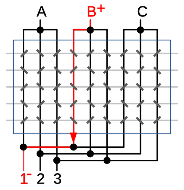
  12. Core memories typically used a "matrix" approach to reduce the number of circuits required to drive the X and Y select lines. The diagram below demonstrates this technique for the vertical lines in a hypothetical 9×5 core array. There are three "high" drivers (A, B and C), and three "low" drivers (1, 2 and 3). If driver B is energized positive and driver 1 is energized negative, current flows through the core line highlighted in red. By selecting a different pair of drivers, a different line is energized. In a large array, this approach significantly reduces the number of line drivers required.

    The "matrix" approach reduces the number of line drivers required.

    The "matrix" approach reduces the number of line drivers required.

    When using a matrix approach, each line must have diodes to prevent "sneak paths" through the cores. To see the need for diodes, note that in the example above current could flow from B to 2, up to A and finally down to 1, for instance, incorrectly energizing multiple lines and flipping the wrong cores. By putting diodes on each line, reverse current paths such as 2 to A can be blocked. Also note that writing core memory requires current pulses in the opposite direction from reading. Supporting this requires additional diodes in the opposite direction. 

  13. Because the characteristics of ferrite cores change with temperature, the memory module adjusts the current based on temperature, from 260 mA at 10 °C to 180 mA at 70 °C. A sensor in the stack detects the temperature, causing a TCV regulator (Temperature Controlled Voltage) to generate a voltage ranging from 6 V at 10 °C to 4 V at 70 °C. The TCV control voltage is fed into each EI module, causing the current to drop 1.33 mA per °C.  

  14. It's unclear why the driver boards use EI modules as well as ID-2 (Inhibit Driver) modules, since a separate board implements the inhibit drivers. The earlier schematics show just the EI modules. (See Laboratory Maintenance Instructions for LVDC Vol. II (1965) page 10-164 for the schematics.) The inhibit driver is similar to the current sink in the EI driver, so I suspect the ID-2 module is being used to boost the current.  

  15. For reference, this footnote provides details of the Y driver signal routing. There are 8 high drive signals and 8 low drive signals generating the 64 Y select lines through the core stack. However, the current through the select line needs to go both ways, so cores can be flipped both directions. Thus, the drive signals are in pairs, one from the "E" side (voltage source) of the EI chip and one from the "I" side (current sink). These 32 signals go from the driver board to the diode matrix through two 16-wire flat cables. The diode board is connected to 64 Y select lines, but each line has two ends. These 128 connections are through four 32-wire flat cables, two on the left and two on the right. The two cables connected to the front side of the diode matrix wrap around to the far side of the stack, while the two cables connected to the back side of the diode matrix go to the near side of the stack. Thus, alternating select lines go through the stack in opposite directions. 

  16. The X and Y diode matrices use a different wiring topology. There are 64 Y lines through the core stack. They are matrixed with 8 drivers at one end and 8 at the other end. The Y board has a diode pair (electrically) at each end of the 64 Y lines, so it has 256 diodes and 128 wires to the Y lines. (Because a line needs to be driven in either direction, one diode is required in each direction, making a pair at each end.)

    On the other hand, there are 128 X lines through the core stack, matrixed with 16 drivers at one end and 8 at the other end. To avoid doubling the number of diodes used, the X board only has a diode pair at one end of each of the 128 X lines. At the other end, groups of 8 X lines are tied together directly, forming 16 groups with one diode pair is used for each group. Thus, there are 256 diodes in the matrix, as well as 32 diodes associated with the 16 groups. As far as wires between the diode matrix and the core stack, there are 128 wires for the diode-connected end, and 32 wires corresponding to the grouped end. See Figures 10-42 and 10-43 in the Laboratory Maintenance Instructions for LVDC Vol. II (1965) for schematics.

    The X driver board is connected to other boards and the core stack through multiple flex cables. The cable on the right links the driver board to the rest of the computer via the I/O board. The top edge of the board has a 24-wire flex cable to the diode matrix, with a second 24-wire cable at the bottom. At the bottom, another smaller flex cable receives signals from the timing board underneath the core stack. The flex cables between the diode matrices and the core stack are not visible: there is a 16-wire cable and a 64-wire cable to the stack at the top and similar cables at the bottom.

    There is an important difference between the X and Y wiring. The four flat cables between the X diode matrix and the core planes went vertically, from the top and bottom of the matrix. The flat cables from the Y diode matrix went horizontally, from the sides of the matrix. In this way, the X and Y cables were attached to orthogonal sides of the core planes, connecting to the orthogonal X and Y wires. 

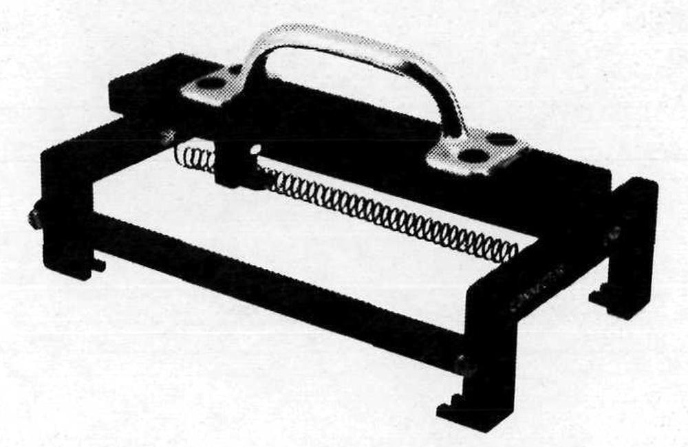
  17. A special handle was produced to insert, remove, or carry the memory module. Because the memory modules were delicate and mounted with little clearance, this tool was developed to manipulate the module safely. This handle slides over the four shoulder screws on top of the module and latches into place.

    The special carrying handle for the memory module. From Laboratory Maintenance Instructions for LVDC Vol. II page 4-5.

    The special carrying handle for the memory module. From Laboratory Maintenance Instructions for LVDC Vol. II page 4-5.


  18. One interesting feature of the LVDC was that memory modules could be mirrored for reliability. In "duplex" mode, each word was stored in two memory modules. If one module had an error, the correct word could be retrieved from the other module. While this provided reliability, it cut the memory capacity in half. Alternatively, memory modules could be used in "simplex" mode, with each word stored once.

    Note that the LVDC's circuitry was triply-redundant to detect and correct errors. However, memory only needed to be doubly redundant because parity indicated which value was incorrect. The LVDC used odd parity. Odd parity had the advantage that parity would catch a word that was stuck all 0's or all 1's. One interesting feature of the simplex and duplex memory modes is that the software could switch between them while running, even setting separate modes for instructions and data. This allowed some words to be stored in simplex mode while more important words were stored in duplex mode. However, it appears that in actual use, the entire memory would be duplexed rather than specific parts. 

Inside the digital clock from a Soyuz spacecraft

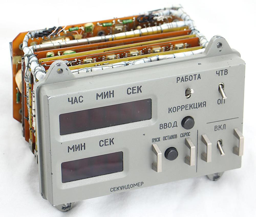
We recently obtained a clock that flew on a Soyuz space mission.1 The clock, manufactured in 1984, is much more complex inside than you'd expect, with over 100 integrated circuits on ten circuit boards. In this blog post, I examine the clock's circuitry and find that it needed so many chips because it was implemented with simple TTL logic. The clock also provides a glimpse into the little-known world of Soviet aerospace electronics and how it compares to American technology.

"Onboard space clock" from a Soyuz mission. The clock provides the time, an alarm, and a stopwatch.

"Onboard space clock" from a Soyuz mission. The clock provides the time, an alarm, and a stopwatch.

The Soyuz series of spacecraft was designed for the Soviet space program as part of the race to the Moon. Soyuz first flew in 1966 and has made more than 140 flights over the past 50 years. The spacecraft (below) consists of three parts. The round section on the left is the orbital or habitation module, holding cargo, equipment, and living space. The descent module in the middle is the only part that returns to Earth; the astronauts are seated in the descent module during launch and reentry. Finally, the service module on the right has the main engine, solar panels, and other systems.

Soyuz TMA-7 spacecraft departing from the International Space Station, 2006. Photo from NASA.

Soyuz TMA-7 spacecraft departing from the International Space Station, 2006. Photo from NASA.

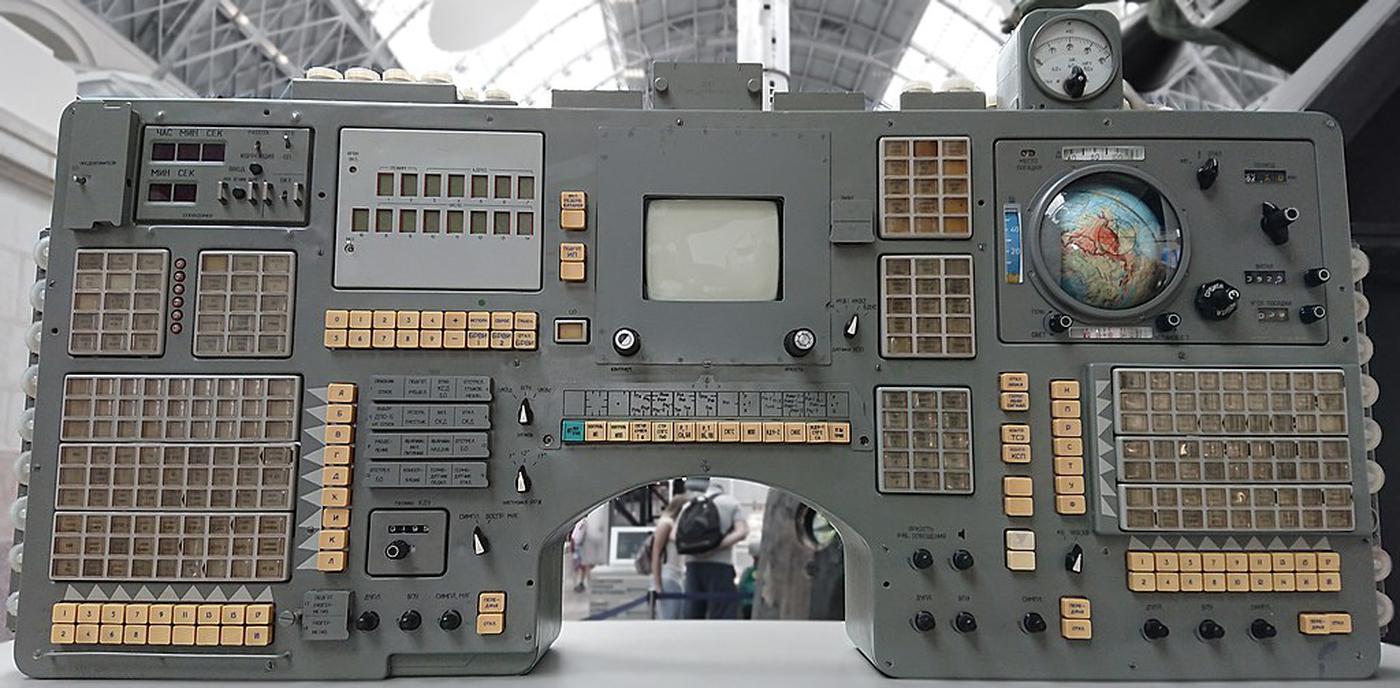
The descent module contains the spacecraft's control panel (below).2 Note the digital clock in the upper left. Early Soyuz spacecraft used an analog clock, but from 1996 to 2002, the spacecraft used a digital clock.3 The digital clock was also used in the Mir space station. The clock was eliminated from later Soyuz spacecraft, which used two computer screens on the control panel in place of the earlier controls.

Control panel from a Soyuz spacecraft. The digital clock is in the upper left of the panel. The screen in the middle is a TV monitor. Photo from Stanislav Kozlovskiy, CC BY-SA 4.0.

Control panel from a Soyuz spacecraft. The digital clock is in the upper left of the panel. The screen in the middle is a TV monitor. Photo from Stanislav Kozlovskiy, CC BY-SA 4.0.

A closer look at the clock

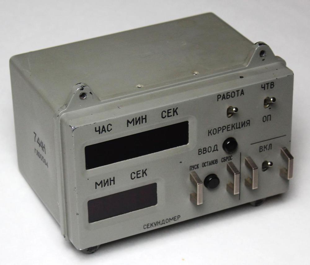
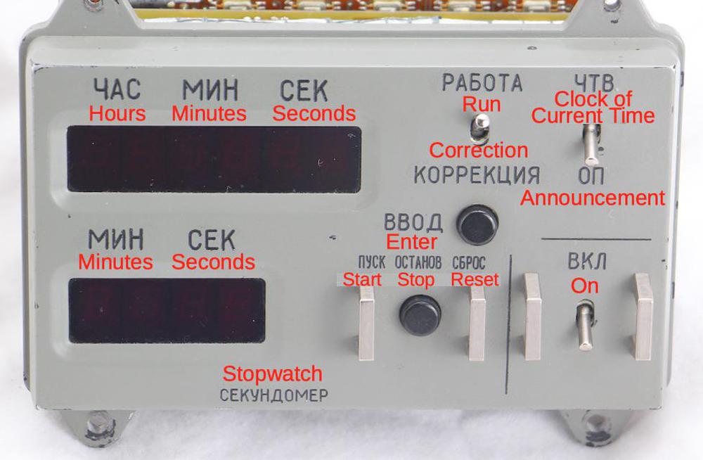
The diagram below shows the clock's labels translated into English. The clock has three functions: the time, an alarm, and a stopwatch. The "Clock of Current Time"5 mode shows the current Moscow time on the six upper LED digits, while "Announcement" shows the alarm time. The alarm can be set to a particular time; at that time, the clock triggers a relay activating an external circuit in the spacecraft.4 The clock is set using the "Correction" mode; digits are incremented using the "Enter" button. The lower half of the unit is the stopwatch; the bottom four LEDs display elapsed minutes and seconds. The lower pushbutton stops, starts, or resets the stopwatch.6 Finally, the power switch at the right turns the clock on.

Front of the clock. The red text is the translation of the Russian labels into English.

Front of the clock. The red text is the translation of the Russian labels into English.

We wanted to see what was inside the clock, of course, so Marc unscrewed the cover and removed it from the clock. This revealed a dense stack of circuit boards inside. The clock was much more complex than I expected, with ten circuit boards crammed full of surface-mount ICs and other components. The components are mounted on two-layer printed-circuit boards, a common construction technique. The boards use a mixture of through-hole components and surface-mount components. That is, components such as resistors and capacitors were mounted by inserting their leads through holes in the boards. The surface-mount integrated circuits, on the other hand, were soldered to pads on top of the board. This is more advanced than 1984-era American consumer electronics, which typically used larger through-hole integrated circuits and didn't move to surface-mount ICs until the late 1980s. (American aerospace computers, in contrast, had used surface-mount ICs since the 1960s.)

Space clock from Soyuz with the cover removed.

Space clock from Soyuz with the cover removed.

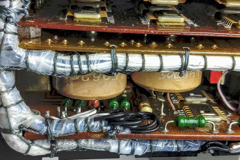
One interesting feature of the clock is that the boards are connected by individual wires that are bundled into wiring harnesses (below). (I expected the boards to plug into a backplane, or be connected by ribbon cables.) The boards have rows of pins along the sides, with wires soldered to these pins. These wires were gathered into bundles, wrapped in plastic, and then carefully laced into wiring harnesses that were tied to the boards.

The clock has point-to-point wires, wrapped into neat harnesses.

The clock has point-to-point wires, wrapped into neat harnesses.

At first, we thought that further disassembly of the clock would be impossible without unsoldering all the wires, but then we realized that the wiring harnesses were designed so the boards could be opened like a book (see below). This allowed us to examine the boards more closely. Inconveniently, some pairs of boards were soldered together at the front by short wires, so we couldn't see both sides of these boards.

The wiring bundles are arranged so the boards can swing apart.

The wiring bundles are arranged so the boards can swing apart.

In the photo above, you can see the numerous integrated circuits in the clock. These are mostly 14-pin "flat pack" integrated circuits in metal packages, unlike contemporary American integrated circuits which were usually packaged in black epoxy. There are also some 16-pin integrated circuits, encased in pink ceramic.

The circuitry inside

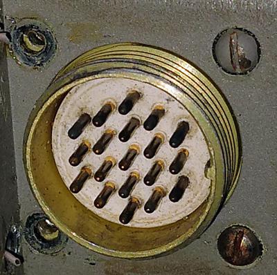
The next step was to examine the circuitry in more detail, which I'll discuss starting at the back of the clock. A 19-pin connector7 linked the clock to the rest of the spacecraft. The spacecraft provided the clock with 28 volts through this connector, as well as external timing pulses and stopwatch control signals. The clock could signal the spacecraft through relay contacts when the alarm time was reached.

This 19-pin connector interfaces the clock to the spacecraft.

This 19-pin connector interfaces the clock to the spacecraft.

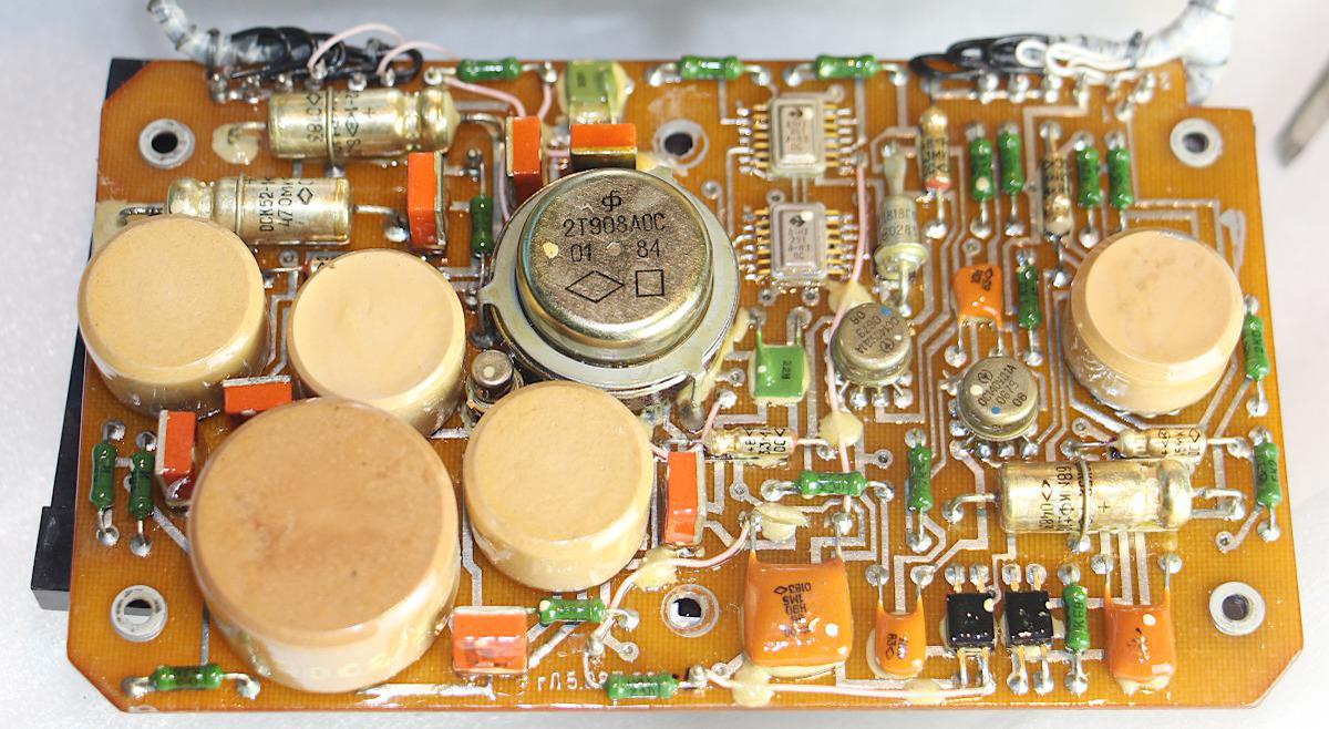
The two circuit boards at the back of the clock are the power supply, which was more complex than I expected. The first board (below) is a switching power supply that converts the spacecraft's 28-volt power to the 5 volts required by the integrated circuits. The round ceramic components are inductors, ranging from simple coils to complex 16-pin inductors. The control circuitry includes two op amps in metal can packages. Two other packages that look like integrated circuits each hold four transistors. Next to them, a bullet-shaped Zener diode sets the output voltage level. The large round switching power transistor is visible in the middle of the board. You might expect the power supply to be a simple buck converter. However, the power supply uses a more complicated design to provide electrical isolation between the spacecraft and the clock. I'm not sure, though, why isolation was necessary.8

Board 1 implements a switching power supply to produce 5 volts for the clock.

Board 1 implements a switching power supply to produce 5 volts for the clock.

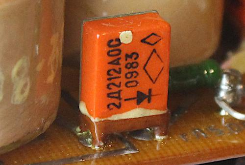
Many of the components in the power supply look different from American components. While American resistors are usually labeled with colored bands, the Soviet resistors are green cylinders with their values printed on them. The Soviet diodes have orange rectangular packages (below), unlike the usual cylindrical American diodes. The power transistor in the middle of the board is round, lacking the metal flanges of American power transistors in "TO-3" packages. I don't think the Soviet packaging is better or worse, but it's interesting to see how components from the two countries diverged.

The power supply uses 1 amp diodes in rectangular orange packages. The "OC" indicates a higher-quality military part.

The power supply uses 1 amp diodes in rectangular orange packages. The "OC" indicates a higher-quality military part.

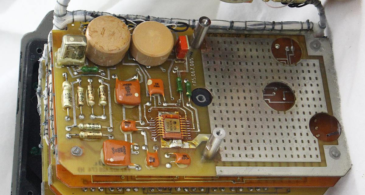
The second board is also part of the power supply, but is much simpler. It has inductors and capacitors to filter the power, as well as a linear voltage regulator chip (pink) to produce 15 volts for the op amp ICs in the first board. The voltage regulator chip has two large metal tabs on the bottom that were soldered to the circuit board to dissipate heat. Strangely, the board has three large holes in the right side. The obvious explanation would be that these holes made room for tall components, a situation that arises on another board. However, there are no components that fit the holes on this board. Thus, I suspect this board was originally designed for a different device and reused in the clock.

Power supply board 2 is half-empty, with the right half apparently acting as a heat sink.

Power supply board 2 is half-empty, with the right half apparently acting as a heat sink.

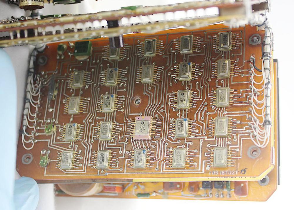
The remaining boards are filled with digital logic integrated circuits. Board 3 (below) and board 5 (which is similar) implement the current time and alarm time functions. Each board contains six BCD counter chips for the six digits (hours, minutes, and seconds).9 In addition, each digit counter requires a logic chip to control when it is incremented and another chip to control when it is reset, depending on whether the clock is being set or is running. (This is one reason why so many chips are required.) The pink chip on the board controls which digit is modified when setting the clock.10

Board 3 is filled with digital logic integrated circuits. Pins on either side connect the board to the wiring harnesses.

Board 3 is filled with digital logic integrated circuits. Pins on either side connect the board to the wiring harnesses.

Board 4 (below) has two functions. First, it controls whether the clock displays the current time or the alarm time. This is implemented with a selection chip for each digit. Second, the board signals the spacecraft when the current time reaches the alarm time. This is implemented with multiple chips to step through each digit, compare the times, and determine if they match. Thus, even though the functions of this board seem simple, they require a whole board of chips. The connections at the bottom of the board link board 4 to board 5. The board is connected to board 3 through the wiring harness.

Board 4 selects between the current time and the alarm time. It also compares the two values to determine when the alarm time has been reached.

Board 4 selects between the current time and the alarm time. It also compares the two values to determine when the alarm time has been reached.

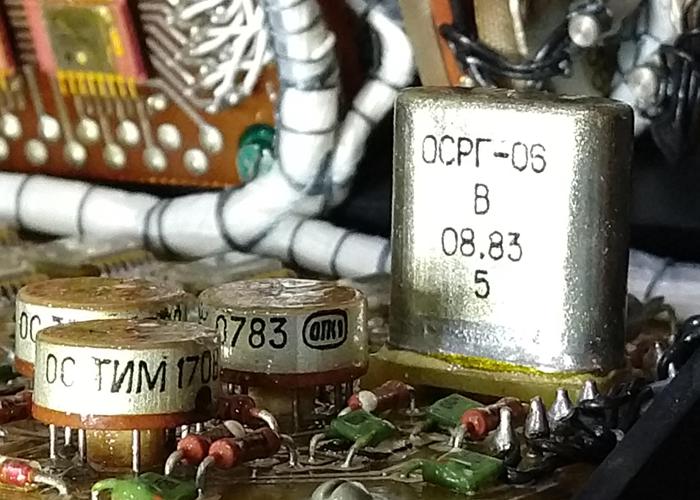
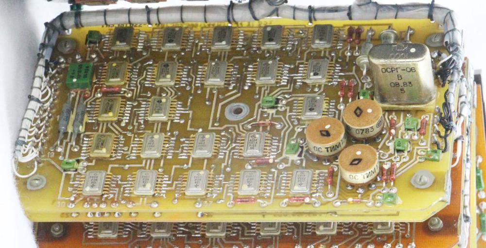
Some of the boards have more circuitry than just digital logic. For instance, boards 6 and 7 have pulse transformers to electrically isolate the control signals fed into the clock through the 19-pin connector. (In modern circuits, this role would be performed by an optoisolator.) These transformers look a bit like mushrooms or miniature water towers, and can be seen in the photo below. Board 7 also has a quartz crystal, the metal rectangle below.11

Board 7 has a 1 MHz crystal that provides the timing signals for the clock. It also has three round pulse transformers that isolate the control signals from the spacecraft.

Board 7 has a 1 MHz crystal that provides the timing signals for the clock. It also has three round pulse transformers that isolate the control signals from the spacecraft.

The two functions of board 7 (below) are to generate the clock's timing pulses and to implement the stopwatch. The quartz crystal generates accurate 1 megahertz pulses. These pulses are reduced to one-second pulses by six BCD counters; each counter chip divides the frequency by 10. These timing pulses are used by the rest of the clock. To implement the stopwatch, the board has four BCD counters for the four digits. It also has control logic to start, stop, and reset the stopwatch. The three pulse transformers allow the spacecraft to control the stopwatch when certain events happen. Additional chips handle these mode changes.

Board 7 contains the stopwatch circuitry, as well as the quartz crystal that generates timings for the whole clock. Wires along the front connect the board to Board 6.

Board 7 contains the stopwatch circuitry, as well as the quartz crystal that generates timings for the whole clock. Wires along the front connect the board to Board 6.

Boards eight and nine drive the LED displays. Each LED digit requires a chip to illuminates the appropriate segments of the 7-segment LED based on the BCD (binary-coded decimal) value. These BCD-to-7-segment driver chips are the pink 16-pin chips on the board.12 Since the clock displays 10 digits in total, 10 driver chips are used. Eight driver chips are on board 8, while board 9 has two chips along with numerous current-limiting resistors for the LEDs. The switches to control the clock are also visible in the photo below.

Board 8 is an LED driver board holding eight 7-segment driver chips. Board 9 (underneath) has two more driver chips and many resistors.

Board 8 is an LED driver board holding eight 7-segment driver chips. Board 9 (underneath) has two more driver chips and many resistors.

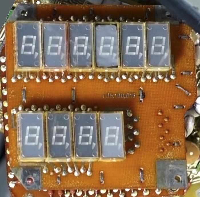
Finally, board 10 (below) holds the ten LED digits. Each digit consists of a seven-segment LED, along with a comma. I think one of the commas is wired up to indicate something; we'll find out what when we power up the clock.

Board 10 holds the ten LED digits. Photo from Marc Verdiell.

Board 10 holds the ten LED digits. Photo from Marc Verdiell.

Soviet integrated circuits

Next, I'll discuss the integrated circuits used in the clock. The clock is built mostly from TTL integrated circuits, a type of digital logic that was popular in the 1970s through the 1990s. (If you've done hobbyist digital electronics, you probably know the 7400-series of TTL chips.) TTL chips were fast, inexpensive and reliable. Their main drawback, however, was that a TTL chip didn't contain much functionality. A basic TTL chip contained just a few logic gates, such as 4 NAND gates or 6 inverters, while a more complex TTL chip implemented a functional unit such as a 4-bit counter. Eventually, TTL lost out to CMOS chips (the chips in modern computers), which use much less power and are much denser.

Because each chip in the Soyuz clock didn't do very much, the clock required many boards of chips to perform its functions. For example, each digit of the clock requires a counter chip, as well as a couple of logic chips to increment and clear that digit as needed, and a chip to drive the associated 7-segment LED display. Since the clock displays 10 digits, that's 40 chips already. Additional chips handle the buttons and switches, implement the alarm, keep track of the stopwatch state, run the oscillator, and so forth, pushing the total to over 100 chips.

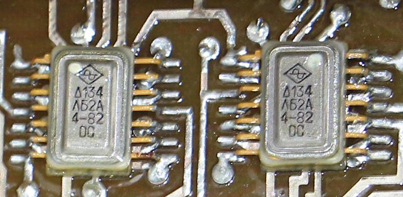
One nice thing about Soviet ICs is that the part numbers are assigned according to a rational system, unlike the essentially random numbering of American integrated circuits.13 Two letters in the part number indicate the function of the chip, such as a logic gate, counter, flip flop, or decoder. For example, the IC below is labeled "Δ134 ΛБ2A". The series number, 134, indicates the chip is a low-power TTL chip. The "Л" (L) indicates a logic chip (Логические), with "ЛБ" indicating NAND/NOR logic gates. Finally, "2" indicates a specific chip in the ЛБ category. (The 134ЛБ2 chip's functionality is two 4-input NAND gates and an inverter, a chip that doesn't have an American counterpart.) 14

Two integrated circuits inside the clock.

Two integrated circuits inside the clock.

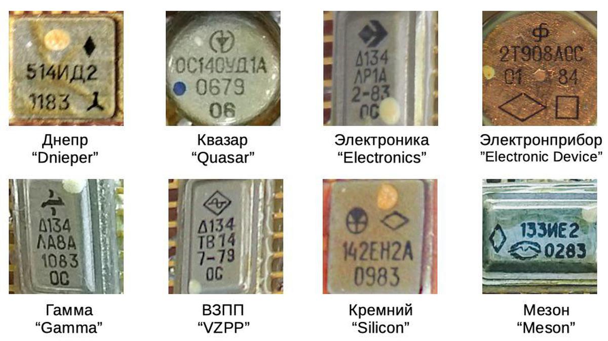
The logos on the integrated circuits reveal that they were manufactured by a variety of companies. Some of the chips in the clock are shown below, along with the name of the manufacturer and its English translation. More information on Soviet semiconductor logos can be found here and here.

By looking up the logo on each chip, the manufacturer can be determined.

By looking up the logo on each chip, the manufacturer can be determined.

Comparison with US technology

How does the Soyuz clock compare with US technology? When I first looked at the clock I would have guessed it was manufactured in 1969, not 1984, based on the construction and the large number of simple flat-pack chips. In comparison, American technology in 1984 produced the IBM PC/AT and the Apple Macintosh. It seemed absurd for the clock to use boards full of TTL chips a decade after the US had produced single-chip digital watches.16 However, the comparison turned out to be not so simple.

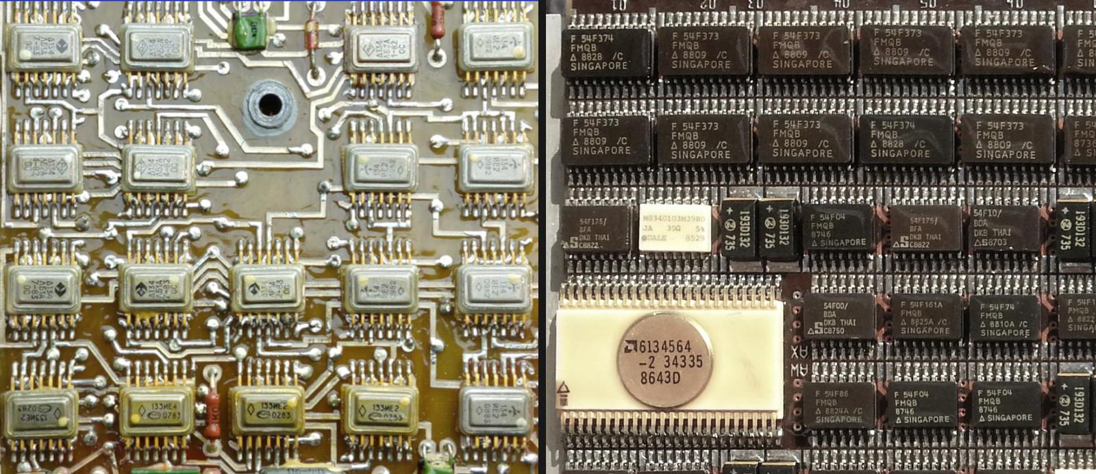
To compare the Soyuz clock with contemporary 1980s American space electronics, I looked at a board from the Space Shuttle's AP-101S computer.17 The photo below shows circuitry from the Soyuz clock (left) and the Shuttle computer (right). Although the Shuttle computer is technologically more advanced, the gap was smaller than I expected. Both systems were built from TTL chips, although the Shuttle computer used a faster generation of chips. Many Shuttle chips are slightly more complex; note the larger 20-pin chips at the top of the board. The large white chip is significantly more complex; it is an AMD Am2960 memory error correction chip. The Shuttle's printed-circuit board is more advanced, with multiple layers rather than two layers, allowing the chips to be packed 50% more densely. At the time, the USSR was estimated to be about 8 to 9 years behind the West in integrated circuit technology;15 this is in line with the differences I see between the two boards.

The Soyuz clock board (left) and Space Shuttle computer board (right), to the same scale. Both use surface-mount TTL chips.

The Soyuz clock board (left) and Space Shuttle computer board (right), to the same scale. Both use surface-mount TTL chips.

What surprised me, though, was the similarities between the Shuttle computer and the Soviet clock. I expected the Shuttle computer to use 1980s microprocessors and be a generation ahead of the Soyuz clock, but instead the two systems both use TTL technology, and in many cases chips with almost identical functionality. For example, both boards use chips that implement four NAND gates. (See if you can find the 134ΛБ1A chip on the left and the 54F00 on the right.)

Conclusion

Why does the Soyuz clock contain over 100 chips instead of being implemented with a single clock chip? Soviet integrated circuit technology was about 8 years behind American technology and TTL chips were a reasonable choice at the time, even in the US. Since each TTL chip doesn't do very much, it takes boards full of chips to implement even something simple like a clock.

The next step will be to power up the clock and see the clock in operation. I've been studying the power supply so we can make this happen. I plan to write more about the power supply and other parts of the clock, so follow me @kenshirriff for details. also have an RSS feed. Until then, you can watch Marc's video showing the disassembly of the space clock:

Notes and References

  1. CuriousMarc obtained the clock from an auction and it was advertised as flown to space, but I don't know which mission it was flown on. The date codes on the components inside the clock are mostly from 1983, with one from 1984, so the clock was probably manufactured in 1984. The Russian name for the clock is "Бортовые Часы Космические" (Onboard Space Clock), which is abbreviated as "БЧК". 

  2. The photo of the Soyuz console was mislabeled as from Soyuz 7K-VI. However, that mission was in the 1960s and the Soyuz-7K console was much different. A photo of the Soyuz-7K console is in this Russian article

  3. The digital clock was used in the Soyuz-TM version of the spacecraft. This version of the console was known as Neptune (Нептун). For details on Soyuz consoles, see The Integrated Information Display System for the Soyuz-TMA. Two Russian documents are this and (this. The analog clock can be seen in a Scott Manley video here and in some photos by Steve Jurvetson. 

  4. Most of the description of how the clock works is based on my reverse engineering, so I don't guarantee that everything in this post is accurate. When we power up the clock, I'll find out what I got wrong :-) 

  5. The clock has the label "ЧТВ", which is an abbreviation for "Часы Текущего Времени". The Soyuz Crew Ops Manual translates this as "Clock of Current Time". 

  6. The Soyuz Crew Ops Manual has some information on the clock on page 35. According to the manual, the stopwatch is controlled automatically during the propulsion system engine burn timing, to measure the time between the Engine Fire command and the Engine Cut Off command. It also automatically measures the time during descent until contact. 

  7. The 19-pin connector was a standard Soviet military connector of type RS19TV (РС19ТВ in Cyrillic). I was able to find a matching connector on eBay, which we will use for powering the clock. 

  8. Cell-phone chargers, for instance, use isolated power supplies for safety, to protect the user from the dangerous 120-volt line voltage. The clock, however, is powered with 28 volts, so there's no obvious reason for electrical isolation. (The Apollo Guidance Computer's power supply, for example, used a non-isolated switching power supply.) 

  9. The clock uses a BCD counter chip for each digit with some exceptions. The top hours digit only goes to "2" (for a 24-hour clock), so two flip flops are used instead of a counter. The top digit for minutes and seconds needs to roll over at 6 (i.e. 60 seconds/minutes), so the clock uses a divide-by-12 chip similar to the 7492 chip. (The chip can be configured to roll over at 6 rather than 12.) 

  10. The pink chip on board 3 is a К134ИД6 decimal decoder, which selects one of 10 outputs based on the 4-bit BCD value fed into it. (The part number ИД indicates a decoder, Дешифраторы.) This chip is a copy of the American 74L42 chip. For some reason, the 16-pin integrated circuits are in pink ceramic packages, while the more common 14-pin integrated circuits are in metal packages. 

  11. The Soyuz Crew Ops Manual (page 35) specifies the clock's accuracy as 30 seconds per day, which isn't very good. In comparison, a low-cost Timex quartz watch from the early 1970s was accurate within 15 seconds per month. According to the manual, the clock could be synchronized to external time pulses. During launch/injection and autonomous orbital flight phases, the clock was synchronized to the Program-Timing Control Equipment (АПВУ). It could also be synchronized to the TV unit (KЛ110). 

  12. LED displays often use multiplexing, where one driver chip is shared across all the digits and the display rapidly cycles through the digits. This reduces the number of chips and resistors required. I'm not sure why the clock uses separate drivers instead of multiplexing. 

  13. For more information on Soviet integrated circuits, including the ones used in the clock, see the databook Интегральные микросхемы и их зарубежные аналоги (Integrated circuits and their foreign counterparts). 

  14. The Soviet IC designation system is described in detail on Wikipedia. There are a few complications that make a chip's designation different from the labels printed on the chip. Because Л and П (Cyrillic L and P) look similar on small chips, the chip labels use Λ (Greek L) in place of Л (Cyrillic L). The Greek D (Δ) may replace Cyrillic D (Д) to avoid confusion with Cyrillic А. Moreover, names for commercial chips start with K, unlike the military chips used in the clock. Thus, a chip labeled "Δ134 ΛБ2A" appears in databooks and on the web under the name "К134ЛБ2". 

  15. Two CIA reports (1974 and 1986) provide information on the lag between Soviet IC technology and Western technology. 

  16. US manufacturers implemented clocks on a single chip in the early 1970s. Mostek introduced a single-chip digital clock chip in 1972, the Mostek MM5017. In 1974, Intel introduced a watch using a low-power CMOS chip, the Intel 5810 In other words, the Soyuz clock could (roughly) have been replaced with a single chip a decade earlier. 

  17. The AP-101S computer in the Space Shuttle was part of IBM's System/4π line of avionics computers. This 64-pound computer was built from TTL integrated circuits, using the 74F00 series (Fairchild's FAST line) for improved performance. (Its memory, however, was built from high-capacity CMOS chips.) The AP-101S computer was an updated version of the AP-101B used in the earlier Space Shuttle flights. (See The new AP101S general-purpose computer (GPC) for the space shuttle and Space Shuttle Avionics Upgrade.)

    At first, it surprised me that they designed both Shuttle computers from low-complexity TTL chips, but it made sense when the design of the earlier AP-101B computer started in 1972. Back in the 1970s, minicomputers were commonly built from TTL chips because microprocessors were new and much slower than TTL. The first Shuttle computer achieved a speed of 0.42 MIPS. This performance was respectable in 1972 but poor by 1981, when the Shuttle first flew.

    To improve performance, a redesign of the computer started in 1982. The updated AP-101S computer stuck with TTL, so its performance improved only moderately, to 1.27 MIPS, slightly slower than the Motorola 68010 (1982) which ran at 2.4 MIPS. Unfortunately, the gap between TTL computers and microcomputers got exponentially worse, following Moore's law. By 1991, when the AP-101S first flew, the Motorola 68040 ran at 44 MIPS. And by the end of the Shuttle program in 2011, the Intel Core i7 processor ran at 100,000 MIPS, many orders of magnitude faster than the Shuttle computer.

    So why did the Space Shuttle use mostly-obsolete TTL technology in the 1980s redesign? One reason was backward compatibility. Since the first Shuttle computer used the proprietary IBM 4π architecture, it couldn't be replaced by an off-the-shelf microprocessor. Reliability was another motivation for TTL. Commerical microprocessors weren't designed for the reliability needs of space systems and lacked features such as radiation resistance and parity-protected caches. Finally, the aerospace development cycle is very long; although the Shuttle computer redesign started in 1982, the computer wasn't used on a flight until 1991 and remained in use until 2011. The point is that there were reasons to build aerospace systems from TTL, even though microprocessors were much faster, more compact, and lower power.