Iconic consoles of the IBM System/360 mainframes, 55 years old

The IBM System/360 was a groundbreaking family of mainframe computers announced on April 7, 1964. Designing the System/360 was an extremely risky "bet-the-company" project for IBM, costing over $5 billion. Although the project ran into severe problems, especially with the software, it was a huge success, one of the top three business accomplishments of all time. System/360 set the direction of the computer industry for decades and popularized features such as the byte, 32-bit words, microcode, and standardized interfaces. The S/360 architecture was so successful that it is still supported by IBM's latest z/Architecture mainframes, 55 years later.

Prior to the System/360, IBM (like most computer manufacturers) produced multiple computers with entirely incompatible architectures. The System/360, on the other hand, was a complete line of computers sharing a single architecture. The fastest model in the original lineup was 50 times as powerful as the slowest,1 but they could all run the same software.2 The general-purpose System/360 handled business and scientific applications and its name symbolized "360 degrees to cover the entire circle of possible uses."34

Large computer room with an IBM System/360 Model 85. The CPU, the double-H unit in the center, weighed over 7 tons.
Cabinets in front are core memory storage, holding 256 kilobytes each.
Cabinets on the right are I/O channels, connected to I/O devices at the back:
tape drives, printers, disk drives, and card readers. Photo from IBM.

Large computer room with an IBM System/360 Model 85. The CPU, the double-H unit in the center, weighed over 7 tons. Cabinets in front are core memory storage, holding 256 kilobytes each. Cabinets on the right are I/O channels, connected to I/O devices at the back: tape drives, printers, disk drives, and card readers. Photo from IBM.

Although the S/360 models shared a common architecture, internally they were completely different to support the wide range of cost and performance levels. Low-end models used simple hardware and an 8-bit datapath while advanced models used features such as wide datapaths, fast semiconductor registers, out-of-order instruction execution, and caches. These differences were reflected in the distinctive front panels of these computers, covered with lights and switches.

This article describes the various S/360 models and how to identify them from the front panels. I'll start with the Model 30, a popular low-end system, and then go through the remaining models in order. Conveniently IBM assigned model numbers rationally, with the size and performance increasing with the model number, from the stripped-down but popular Model 20 to the high-performance Model 195.

IBM System/360 Model 30

The photo below shows a Model 30, one of the lower-end S/360 machines, with 8 to 64 kilobytes of magnetic core memory. The CPU cabinet was 5 feet high, 2'6" wide and 5'8" deep and weighed 1700 pounds, enormous by modern standards but a smaller computer for the time. System/360 computers were built from fingernail-sized modules called Solid Logic Technology (SLT) that contained a few transistors and resistors, not as dense as integrated circuits. Although the Model 30 was the least powerful model when the System/360 line was announced, it was very popular and profitable, renting for $8,000 a month and bringing IBM over a billion dollars in revenue by 1972.

IBM S/360 Model 30 on display at the Computer History Museum.

IBM S/360 Model 30 on display at the Computer History Museum.

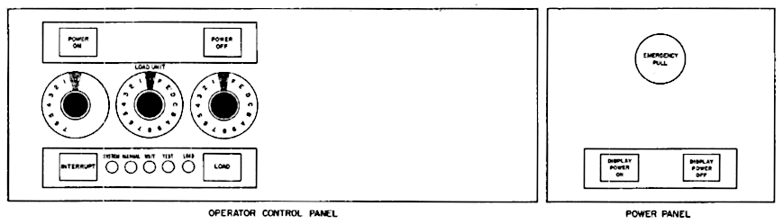
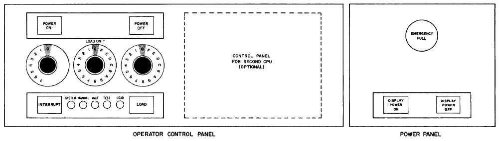
You might wonder why these computers had such complex consoles.5 There were three main uses for the console.6 The first use was basic "operator control" tasks such as turning the system on, booting it, or powering it off, using the controls shown below. These controls were consistent across the S/360 line and were usually the only controls the operator needed. The three hexadecimal dials selected the I/O unit that held the boot software.7 Once the system had booted, the operator generally typed commands into the system rather than using the console.

The "operator control" section of the control panel was used for basic tasks such as booting the system (called Initial Program Load or IPL). The buttons provided "Power On", "Power Off", "Interrupt", and "Load", while the lights indicated if the system was running.

The "operator control" section of the control panel was used for basic tasks such as booting the system (called Initial Program Load or IPL). The buttons provided "Power On", "Power Off", "Interrupt", and "Load", while the lights indicated if the system was running.

The second console function was "operator intervention": program debugging tasks such as examining and modifying memory or registers and setting breakpoints. The Model 30 console controls below were used for operator intervention. To display memory contents, the operator selected an address with the four hexadecimal dials on the left and pushed the Display button, displaying data on the lights above the dials. To modify memory, the operator entered a byte using the two hex dials on the far right and pushed the Store button. (Although the Model 30 had a 32-bit architecture, it operated on one byte at a time, trading off speed for lower cost.) The Address Compare knob in the upper right set a breakpoint.

The lower part of the Model 30 console was used for operator intervention. Note the binary-to-hexadecimal conversion chart below the hexadecimal dials.

The lower part of the Model 30 console was used for operator intervention. Note the binary-to-hexadecimal conversion chart below the hexadecimal dials.

The third console function was supporting system maintenance and repair performed by an IBM customer engineer. The customer engineering displays took up most of the console and provided detailed access to the computer's complex internal state. On the Model 30 console above, the larger middle knob (Display Store Selection) selected any of the internal registers for display or modification. The rows of lights below showed the microcode instruction being executed from "read only storage" and operations on the I/O channel.

Closeup of the IBM S/360 Model 30 console showing indicators for the microcode (read only storage) and I/O channel. These registers were used internally and were not visible to the programmer.

Closeup of the IBM S/360 Model 30 console showing indicators for the microcode (read only storage) and I/O channel. These registers were used internally and were not visible to the programmer.

The consoles also included odometer-style usage meters, below the Emergency Power Off knob.10 The standard IBM rental price covered a 40-hour week and a customer would be billed extra for excess usage. However, customers were not charged for computer time during maintenance. When repairing the system, the customer engineer turned the keyswitch, causing time to be recorded on the lower service meter instead of the customer usage meter.

The Emergency Power Off knob shut down the entire system. Below it were the usage meters. The keyswitch selected the maintenance meter, so customers would not be charged for computer operation during maintenance.

The Emergency Power Off knob shut down the entire system. Below it were the usage meters. The keyswitch selected the maintenance meter, so customers would not be charged for computer operation during maintenance.

IBM System/360 Model 20

Moving now to the bottom of the S/360 line, the Model 20 was intended for business applications.9 Its storage was limited, just 4K to 32K bytes of core storage, and it was extremely slow even by 1960s standards, performing about 5700 additions per second. This slow CPU was enough to generate business reports from punch cards since the card reader only read 8 cards per second. To reduce its price, the Model 20 implemented a subset of the S/360 instructions and used half-sized registers,8 making it incompatible with the rest of the S/360 line. Despite its limitations, the Model 20 was the most popular S/360 model due to its low price, with more than 7,400 Model 20s in operation by the end of 1970. The monthly rental price of the Model 20 started at $1280 with the purchase price starting at $62,710.

The low-end IBM System/360 Model 20 computer. The computer and its console were smaller than other systems in the S/360 line. Photo by Waelder, CC BY-SA 2.5.

The low-end IBM System/360 Model 20 computer. The computer and its console were smaller than other systems in the S/360 line. Photo by Waelder, CC BY-SA 2.5.

The Model 20's small console (above) allowed the operator to turn the computer on and off, load a program, and so forth. A few rows of lights showed the contents of the computer's registers and hexadecimal dials loaded a byte (left two dials) into a memory address (next four dials). Another dial let the operator debug a program by modifying memory, setting a breakpoint, or single-stepping through a program. The Emergency Power Off knob and usage meters are at the far right.

The Model 20 hid a separate control panel for customer engineers behind a cover (below). This panel provided additional controls and lights for diagnostics and access to the microcode. Because the Model 20 was simpler internally than the Model 30, not as much information needed to be displayed to the customer engineer.

Customer engineering control panel for the IBM S/360 Model 20. Photo by Ben Franske, CC BY-SA 2.5.

Customer engineering control panel for the IBM S/360 Model 20. Photo by Ben Franske, CC BY-SA 2.5.

IBM System/360 Model 22

The Model 22 was a cut-down version of the Model 30 at 1/3 the price, providing about 5 times the performance of the Model 20. It was the last S/360 computer introduced, announced in 1971. IBM said the Model 22 "combined intermediate-scale data processing capability with small-system economy."

A base Model 22 CPU rented for $850 a month (less than the Model 25 or most Model 20s) with a purchase price of $32,000 to $44,000. A typical configuration with three disk drives, line printer and card reader cost considerably more, renting for about $5,600 or purchased for $246,000. The processing unit weighed 1500 pounds and was about the size of two refrigerators.11 Unlike the Model 20, the Model 22 was compatible with the rest of the S/360 line.

IBM System/360 Model 22. Photo from IBM.

IBM System/360 Model 22. Photo from IBM.

The Model 22's console was very similar to the Model 30's, since the Model 22 was derived from the Model 30. The Model 22 had fewer rows of lights, though, and the bulbs projected from the console in individual holders, rather than being hidden behind the Model 30's flat overlay. Because of its late introduction date, the Model 22 used semiconductor memory rather than magnetic core memory.

IBM System/360 Model 25

The Model 25 was another low-end system, designed to be less expensive than the Model 30 but without the incompatibility of the Model 20. A typical Model 25 rented for $5,330 a month with a purchase price of $253,000. It was introduced in 1968, late in the S/360 line but before the Model 22.

It was a compact system, packaging I/O controllers in the main cabinet (unlike other S/360 systems). Unlike other low-end systems, it had a two-byte datapath for higher performance. One of the Model 25's features was a smaller easy-to-use console; on the Model 25, many operations used the console typewriter rather than the control panel. In the picture below, note the squat control panel, about 2/3 the height of the black computer cabinet behind it. The control panel reused dials for multiple functions (such as address and data), making it more compact than the Model 30 panel.

IBM System/360 Model 25. Photo from IBM.

IBM System/360 Model 25. Photo from IBM.

IBM System/360 Model 40

The Model 40 was a popular midrange model, more powerful than the Model 30. It typically rented for about $9,000-$17,000 per month and brought IBM over a billion dollars in revenue by 1972. For improved performance, the Model 40 used a two-byte datapath (unlike the Model 30, which handled data one byte at a time)

IBM System/360 Model 40. Photo by Daderot.

IBM System/360 Model 40. Photo by Daderot.

In the photo above, you can see that the Model 40 console is considerably more complex than the Model 30 console, reflecting the increased internal complexity of the system. Like the other models, it had three hex dials in the lower right to boot the system. But instead of hex dials for address and data entry, the Model 40 had rows of toggle switches: one for the address and one for the data.

To keep the number of lights manageable, the Model 40 used two "rollers" that allowed each row of lights to display eight different functions. Each roller had an 8-position knob on the right side of the console, allowing a particular register or display to be selected. The knob physically rotated the legend above the lights to show the meaning of each light for the selected function.

Multi-function rollers on the S/360 Model 40 allowed more data to be displayed on the console.

Multi-function rollers on the S/360 Model 40 allowed more data to be displayed on the console.

IBM System/360 Model 44

IBM's competitors in the scientific computing market offered cheaper but faster systems designed specifically for numerical computing. IBM created the Model 44 to address this gap, giving it faster floating point and data acquisition instructions while dropping business-oriented instructions (decimal arithmetic and variable field length instructions).3 These changes made the Model 44 somewhat incompatible with the rest of the S/360 line, but it was 30 to 60 percent faster than the more-expensive Model 50 on suitable workloads. Despite the improved performance, the Model 44 met with limited customer success.

IBM System/360 Model 44 control panel.

IBM System/360 Model 44 control panel.

The Model 44's console was superficially similar to the Model 40's, with toggle switches and two roller knobs, but on the Model 44, one of the rollers changed the function of the toggle switches. The two models were entirely different internally; for higher performance, the Model 44 used a hard-wired control system instead of microcode. It also used a four-byte datapath, moving data twice as fast as the Model 40, so it has had twice as many lights and switches in each row on the console (32 data bits + 4 parity bits).12

One unusual feature of the Model 44's console was a rotary knob (bottom knob on the left) to select floating point precision; reducing the precision increased speed. Another feature unique to the Model 44 was a disk drive built into the side of the computer. The removable disk cartridge held about 1 megabyte of data. The buttons in the lower left of the console controlled the disk drive.

The Model 44 had a disk drive or two in the side of the computer that used a removable IBM 2315 Disk Cartridge. Photo from Model 44 Functional Characteristics.

The Model 44 had a disk drive or two in the side of the computer that used a removable IBM 2315 Disk Cartridge. Photo from Model 44 Functional Characteristics.

IBM System/360 Model 50

The Model 50 had significantly higher performance than the Model 40, partly because it used a four-byte datapath for higher performance. Physically, the Model 50 was considerably larger than the lower models: the CPU with 512 KB of memory was 5 large frames weighing over 3 tons. The Model 50 typically rented for about $18,000 - $32,000 per month. It could be expanded with 8 more megabytes externally; each IBM 2361 "Large Capacity Storage" unit held 2 megabytes of core memory and weighed a ton.

IBM System/360 Model 50 control panel. The dataflow diagram in the upper right illustrates the system's internal design. Photo by Sandstein, CC BY-SA 3.0

IBM System/360 Model 50 control panel. The dataflow diagram in the upper right illustrates the system's internal design. Photo by Sandstein, CC BY-SA 3.0

The Model 50's console was more complex than the Model 40 or Model 44. Like the Model 44, the toggle switches and lights are 32 bits + parity because of the 4-byte datapath. The Model 50 used four roller knobs to support multiple functions on each row of lights. The voltmeter and voltage control knobs in the upper left were used by an IBM customer engineer for "marginal checking". By raising and lowering the voltage levels about 5% and checking for failures, borderline components could be detected and replaced before they caused problems.

Control panel of the IBM System/360 Model 50. This panel has marginal check controls for auxiliary storage in the upper right, replacing the dataflow diagram.

Control panel of the IBM System/360 Model 50. This panel has marginal check controls for auxiliary storage in the upper right, replacing the dataflow diagram.

IBM System/360 Models 60, 62, 65 and 67

The models in the 60 series were very similar, designed for large scale business and scientific computation. Models 60 and 62 were announced at the S/360 launch, but they were never shipped. Competitors announced faster machines so IBM improved the core memory to create the Model 65; it had fast .75μs memory, obsoleting the Model 60 (2μs) and Model 62 (1μs) before they shipped. The Model 65 typically rented for $50,000 a month.

IBM System/360 Model 60 with peripherals. Photo from  IBM 360 System Summary page 10.

IBM System/360 Model 60 with peripherals. Photo from IBM 360 System Summary page 10.

The Model 65's console had much in common with the Model 50, although it had 6 rollers instead of 4 to display more information. The Model 60 and higher models used an eight-byte datapath and storage interleaving for highest memory performance.13 To support the wide datapath, the console had two rows of toggle switches for data, as well as more address toggle switches to support the larger address range. Each roller controlled 36 lights (4 bytes + parity), so the 64-bit registers were split across two rows of lights.

IBM System/360 Model 65. From Michael J. Ross.

IBM System/360 Model 65. From Michael J. Ross.

The Model 67 was announced in 1965 and shipped in 1966 to support the demand for time-sharing systems, computers that could support numerous users at the same time. (Most computers back then were "batch" systems, running a single program at a time.) The Model 67 was essentially a Model 65 with the addition of virtual memory, called Dynamic Address Translation. It supported "on-line" computing with remote users, time-sharing, and multiple concurrent users. Unfortunately, due to delays in releasing the operating system the Model 67 was not a large success, with only 52 installations by the end of 1970.

The 60-series models were physically large, especially with multiple memory units attached. They could also be configured as a two-processor "duplex" multiprocessor, weighing over four tons and occupying about 400 square feet; note the two consoles in the photo below.

IBM System/360 Model 67, duplex system. From IBM System/360 System Summary page 6-13

IBM System/360 Model 67, duplex system. From IBM System/360 System Summary page 6-13

IBM System/360 Models 70 and 75

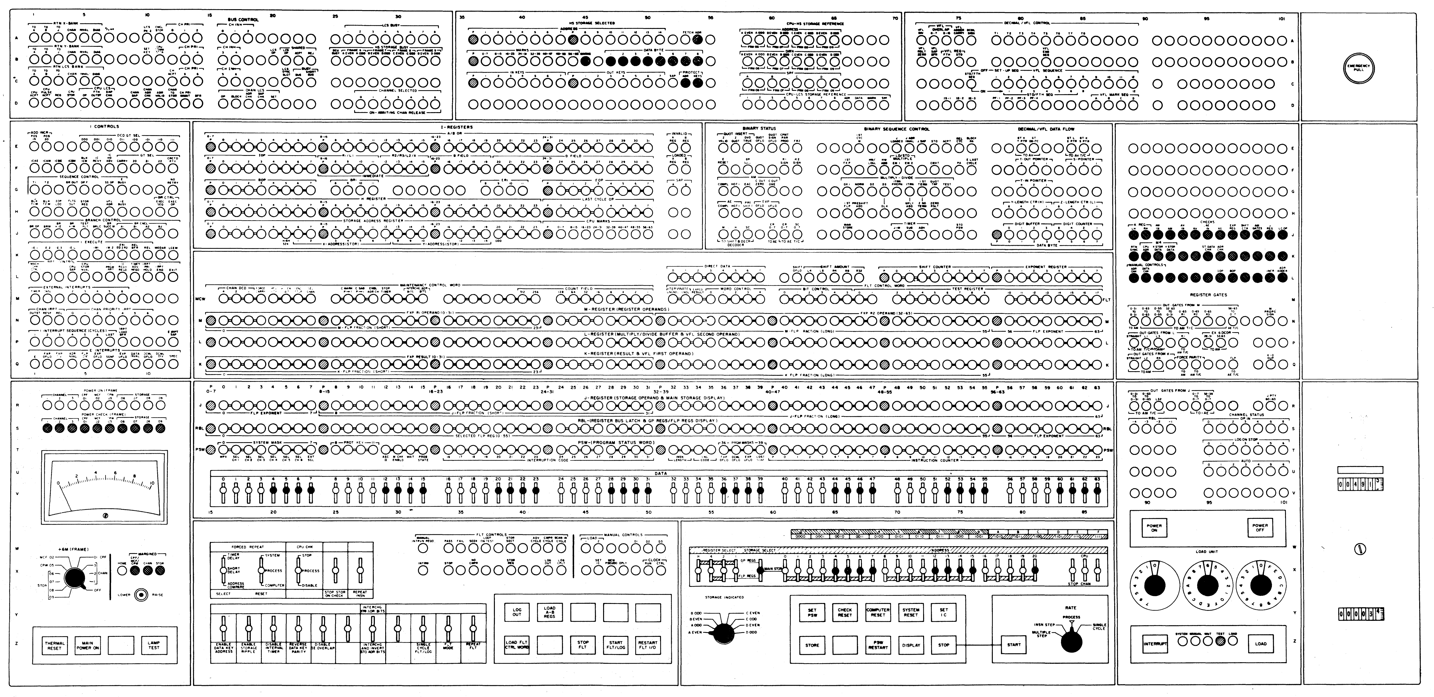
The high-end Model 70 was announced in April 1964, but as with the Model 60, improvements in memory speed caused the Model 70 to be replaced by the faster Model 75 before it shipped. The Model 75's console was much larger than the lower models with a remarkable number of lights, for two reasons.14 First, the Model 75's internal architecture was complex, with multiple data paths and internal registers to improve performance, resulting in more data to display. Second, instead of using rollers to display different functions, the Model 75 displayed everything at once on its vast array of lights.

IBM System/360 Model 75. This version has 1 megabyte of storage in four 2365 Processor Storage units, four of the "fins" off the central spine. From Model 75 Functional Characteristics page 4.

IBM System/360 Model 75. This version has 1 megabyte of storage in four 2365 Processor Storage units, four of the "fins" off the central spine. From Model 75 Functional Characteristics page 4.

I'll point out some of the highlights of the console. The standard operator dials to boot the system were in the lower right (section N), next to the usage meters (P). To examine and modify memory, the operator used the address switches (R), 64 data switches (M), and lights (M). Most of the other sections were for customer engineers. The voltmeter (K) was used for marginal checking. Other sections included bus control (A), high-speed storage (B), variable field length instructions (C), instruction controls (E), and registers (F, L).

The IBM S/360 Model 75 had a very large console. Diagram from Model 75 Functional Characteristics page 14.

The IBM S/360 Model 75 had a very large console. Diagram from Model 75 Functional Characteristics page 14.

The Model 75 had a monthly rental price of $50,000 to $80,000 and a purchase price from $2.2 million to $3.5 million. IBM considered the Model 75 a 1-MIPS computer, executing about 1 Million Instructions Per Second. (This would put its performance a bit below an Intel 80286, or about 1/10,000 the performance of a modern Intel Core I7.)

IBM System/360 Model 85

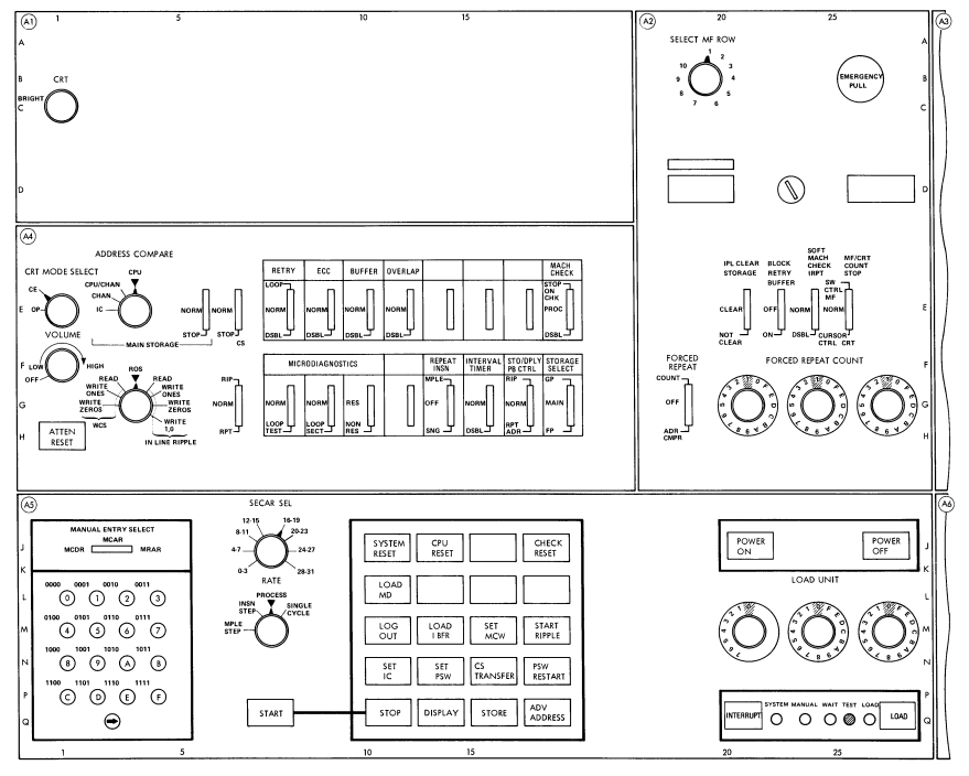
The high-end Model 85 was a later model in the S/360 line, introduced in 1968. Its massive processing unit consisted of a dozen frames and weighed about 7 tons, as shown in the photo at the beginning of the article. A key innovation of the Model 85 was the memory cache to speed up memory accesses. While caches are ubiquitous in modern computers, the Model 85 was the first commercial computer with a main-memory cache. The Model 85 was also IBM's first computer to use integrated circuits (which IBM called Monolithic System Technology or MST). Unfortunately, the Model 85 was not a success with customers; its price was relatively high at a time when the data processing industry was going through a slowdown. As a result, only about 30 Model 85 systems were ever built.

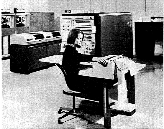
The Model 85 used a radically different approach for the console.15 The control panel of lights and switches was small compared to other S/360 systems. Instead, a CRT display and keyboard were used for many operator functions, visible in front of the operator below. To the left of the operator, an "indicator viewer" replaced most of the panel lights. The indicator viewer combined 240 lights with a microfiche projector that displayed the appropriate labels for ten different configurations, a more advanced version of the rollers that provided the equivalent of 2400 individual lights. The system also included a microfiche document viewer (far left of photo), replacing binders of maintenance documentation with compact microfiche cards.

Console for the IBM System/360 Model 85 at NSA (source).

Console for the IBM System/360 Model 85 at NSA (source).

IBM System/360 Models 90, 91, 92 and 95

The Model 90 was just a footnote in the original S/360 announcement, a conceptual "super computer". The improved Model 92 was announced a few months later but then scaled back to create the Model 91. The Model 91 was intended to compete with the CDC 6600 supercomputer (designed by Cray), but ended up shipping in 1967, about two years after the CDC 6600.16 As a result, the Model 91 was rather unsuccessful with only 15 to 20 Model 91's produced, despite cuts to the $6,000,000 price tag. In comparison, CDC built more than 200 computers in the 6000 series.

The Model 91 was architecturally advanced; it was highly pipelined with out-of-order execution and multiple functional units. Reflecting its complex architecture, the Model 91 had a massive control panel filled with lights and switches. The lower part of the main panel had the "operator intervention" functions, including toggle switches for a 24-bit address and 8 bytes of data. The remainder of the lights showed detailed system status for IBM customer engineers. The basic operator controls (power, boot) were not on the main panel, but on a small panel below and to the right of the main console. (It is visible in the photo below, just to the left of the operator's head.) The operator also used the CRT for many tasks.15

Console of the IBM System/360 Model 91. The very large computer itself is not visible in this photo. Photo source unknown.

Console of the IBM System/360 Model 91. The very large computer itself is not visible in this photo. Photo source unknown.

The Model 91 was a room-filling system as the central processor consisted of seven stand-alone units: the CPU itself, three power supplies (not counting the motor-generator set), a power distribution unit, a coolant distribution unit, and a system console. In addition, an installation had the usual storage control unit, I/O channel boxes, and I/O devices. The Model 91 was the first IBM system to use semiconductor memory, in its small "storage protect" memory but not the main memory.

As for the Model 95, IBM started researching thin-film storage as a replacement for core memory in 1951. After years of difficulty, in 1968 IBM shipped thin-film memory in the Model 95 (which was otherwise the same as the Model 91). Although this was the fastest megabyte memory for many years, IBM sold just two Model 95 computers (to NASA) and then abandoned thin-film memory.

IBM System/360 Model 195

The Model 195 was "designed for ultrahigh-speed, large-scale computer applications." It was a reimplementation of the Model 91 using integrated circuits (called "monolithic circuitry", still in IBM's SLT-style packages), and also included a 32K byte memory cache. It rented for $165,000 to $275,000 a month, with purchase prices from $7 million to $12.5 million. The Model 195's performance was comparable to the CDC 7600 supercomputer, but as with the Model 91, the Model 195 was delivered about two years later than the comparable CDC machine, limiting sales.

The Model 195's console (below) was very similar to the Model 95's. As with the Model 91, the Model 195 used a CRT15 for many operator tasks and had a separate small operator console (not shown). 17

Console for the IBM System/360 Model 195.
This console has the dark color scheme used for S/370 consoles even though it was an S/360 system.
With approximately 2000 light bulbs, the console has complex wiring, visible below the console.
Photo from Science Museum Group.

Console for the IBM System/360 Model 195. This console has the dark color scheme used for S/370 consoles even though it was an S/360 system. With approximately 2000 light bulbs, the console has complex wiring, visible below the console. Photo from Science Museum Group.

Identification at a glance

It can be hard to distinguish the consoles of the common Models 30, 40, 50 and 65. The diagram below shows the main features that separate these consoles, helping to identify them in photographs. The Model 30 had a flat silkscreened panel without individual indicators and toggle switches. It can also be distinguished by the 9 dials at the bottom, and the group of four dials on the right. The Model 40 had two rollers, and the group of four dials on the left. The Model 50 had four rollers, and a voltmeter next to a dozen knobs. The Model 60 had six rollers, and a voltmeter with just a couple knobs.

Common IBM System/360 consoles, with distinguishing features identified. The number of roller knobs on the right (0, 2, 4, or 6) provides a convenient way to tell the models apart.

Common IBM System/360 consoles, with distinguishing features identified. The number of roller knobs on the right (0, 2, 4, or 6) provides a convenient way to tell the models apart.

Conclusion

By modern standards the System/360 computers were unimpressive: the Model 20 was much slower and had less memory than the VIC-20 home computer (1980), while at the top of the line, the Model 195 was comparable to a Macintosh IIFX (1990), with about 1/1000 the compute power of an iPhone X. On the other hand, these mainframes could handle a room full of I/O devices and dozens of simultaneous users. Even with their low performance, they were running large companies, planning the mission to the Moon, and managing the nation's air traffic control.

Mainframe computers aren't thought about much nowadays, but they are still used more than you might expect; 92 of the top 100 banks use mainframes, for instance. Mainframe sales are still a billion-dollar market, and IBM continues to release new mainframes in its Z series. Although these are modern 64-bit processors, amazingly they are still backward-compatible with the System/360 and customers can still run their 1964 programs. Thus, the S/360 architecture lives on, 55 years later, making it probably the longest-lasting computer architecture.

I announce my latest blog posts on Twitter, so follow me @kenshirriff for future articles. I also have an RSS feed.

More information

The book IBM's 360 and Early 370 Systems describes the history of the S/360 in great detail. IBM lists data on each model, including dates, data flow width, cycle time, storage, and microcode size. Another list with model details is here. Diagrams of S/360 consoles are at quadibloc. The article System/360 and Beyond has lots of info. A list of 360 models and brief descriptions is here.

Here are some links for each specific model:

Model 20: Functional Characteristics manual, Field Engineering manuals, Wikipedia.
Model 22: Wikipedia, IBM.
Model 25: Functional Characteristics manual, Wikipedia, Field Engineering manuals.
Model 30: Functional Characteristics manual, Wikipedia, Field Engineering manuals, photos here, here, here, here, here.
Model 40: Functional Characteristics manual, Field Engineering manuals, Wikipedia. Other photos here (from IBM System/360 System Summary page 6-7), here, here. The photo here apparently shows a prototype console with a roller.
Model 44: Functional Characteristics manual, Wikipedia, brochure. The photo here shows an earlier prototype with a different console. Some interesting notes are here.
Model 50: Functional Characteristics manual, Field Engineering manuals, Wikipedia, photos here and here, CuriousMarc video.
Model 65: Functional Characteristics manual, Field Engineering manuals, Wikipedia, photo here.
Model 67: Functional Characteristics manual, Wikipedia, photos here, here.
Model 75: Functional Characteristics manual, Field Engineering manuals (console diagram), Wikipedia.
Model 85: Functional Characteristics manual (console diagram, page 20), Wikipedia.
Model 91: Functional Characteristics manual, Wikipedia. Other photos here, here here here and here.
Model 92: IBM info with photo.
Model 195: Functional Characteristics and Wikipedia, photo here.

Notes and references

  1. Many sources give the eventual performance range of the S/360 range as 200 to 1. However, if you include the extremely slow Model 20, the performance ratio is about 3000 to 1. between the powerful Model 195 and the Model 20. Based on several sources, the Model 20 had the dismal performance of 2 to 5.7 KIPS (thousand instructions per second), while the Model 195 was about 10 to 17.3 MIPS (million instructions per second). The Model 20 started at 4K of storage, while the Model 195 went up to 8 megabytes, a 2000:1 ratio.

    To compare with microprocessor systems, a 6502 performed about 430 KIPS. People claim the iPhone X does 600 billion instructions per second, but those are "neural processor" instructions, so not really comparable; based on benchmarks, about 15 billion instructions per second seems more realistic. 

  2. The System/360 architecture is described in detail in the Principles of Operation. However, the System/360 didn't completely meet the goal of a compatible architecture. IBM split out the business and scientific markets on the low-end machines by marketing subsets of the instruction set. The basic instructions were provided in the "standard" instruction set. On top of this, decimal instructions (for business) were in the "commercial" instruction set and floating point was in the "scientific" instruction set. The "universal" instruction set provided all these instructions plus storage protection (i.e. memory protection between programs). Additionally, cost-cutting on the low-end Model 20 made it incompatible with the S/360 architecture, and the Model 44 was somewhat incompatible to improve performance on scientific applications. 

  3. The IBM System/4 Pi family contained several incompatible models. The high-performance Model EP (Extended Performance) was based on the S/360 Model 44's (somewhat incompatible) instruction set, while other 4 Pi models were entirely incompatible with the S/360 line. 

  4. In 1970, IBM introduced the System/370, with "370" representing the 360 for the 1970s. Similarly, IBM introduced the System/390 in 1990. The initial IBM 370 model numbers generally added 105 to the corresponding S/360 model numbers. For example, the S/370 Models 135, 145, 155, 165 were based on the S/360 Models 30, 40, 50 and 65. The S/370 Model 195 was very similar to the S/360 Model 195.  

  5. Most S/360 models had console lights in round sockets that project from the panel. In contrast, the console lights on the Model 30 were hidden behind a flat silkscreened overlay. This is probably because the Model 30 was designed at IBM's Endicott site, the same site that built the low-end IBM 1401 computer with a similar silkscreened console. Different S/360 models were designed at different IBM sites, and the characteristics of the computer often depended on which site designed the computer.  

  6. The features of the system control panel were carefully defined in the System/360 Principles of Operation pages 117-121, providing a consistent operator experience across the S/360 line. (The customer engineering part of the panel, on the other hand, was not specified and wildly different across the product line.) 

  7. An I/O unit was selected for booting with the three hex dials. The first knob selected the I/O channel, while the next two selected a subchannel on that I/O channel. These unit addresses were somewhat standardized; for instance, a disk drive was typically 190 or 191 while tape drives were 180 through 187 or 280 through 287 if they were on channel 1 or 2 respectively. 

  8. The Model 20 was designed at IBM's Böblingen, Germany site. The Model 20 was radically different in appearance from the other S/360 machines. It also had a different, incompatible architecture. These characteristics are likely a consequence of the Model 20 being designed at a remote IBM site. Regardless, the Model 20 was very popular with customers. 

  9. Although the Model 20 Functional Characteristics manual says that it supported time sharing, this is not timesharing in the normal sense. Instead, it refers to overlapping I/O with processing, essentially DMA. 

  10. While the Emergency Power Off button looks dramatic and was rumored to trigger a guillotine blade through the power cable, its implementation was more mundane. It de-energized a power supply relay, cutting off the system power. Behind the console, a tab popped out of the button when pulled, so the EPO button couldn't be pushed back in until a customer engineer opened the console and pushed the tab back in. 

  11. For exact dimensions of the System/360 units, see the System/360 Installation Manual. While the CPU for a low-end 360 system was reasonably compact, you could easily fill a room once you add a card reader, line printer, a bunch of tape drives, disk storage, I/O channels, and other peripherals. The computers generally consisted of one or more cabinets (called "frames" because they were constructed from a metal frame), about 30"×60". (To make installation easier, the frames were sized to fit through doorways and in freight elevators.) The "main frame" was the CPU, with other frames for power, I/O, memory and other functions. 

  12. The Model 44 was developed by IBM's Data Systems Division in Poughkeepsie, NY in partnership with IBM's Hursley UK site. Since Hursley designed the Model 40 and Poughkeepsie designed the Model 50 and larger systems, this may explain why the Model 44 is similar to the Model 40 in some ways, but closer to the larger systems in other ways, such as the use of a two-byte datapath and hardwired control instead of microcode. 

  13. One of the challenges of the 360 line was that the original models differed in performance by a factor of 50, while raw core memory speeds only differed by a factor of 3.3 (See IBM's 360 and Early 370 Systems page 194.) Several techniques were used to get memory performance to scale with processor performance. First was transferring multiple bytes at a time in larger systems. Second was slowing low-end processors by, for example, using the same core memory for register storage. The third technique was interleaving, splitting the memory into 2 to 8 separate modules and prefetching. With prefetching, as long as accesses were sequential, data would be ready when needed. 

  14. The Model 75 and larger systems abandoned the use of microcode, using a hardwired control that could handle the higher speed. This may be connected with the drastic jump in console complexity between the Model 65 and the Model 75. 

  15. A CRT display was used for the console on the models 85, 91 and 195. (I suspect this was because CRT display technology had advanced by the time these later systems were built.) The models 91 and 195 used a display based on the IBM 2250 Graphics Display Unit. This was a vector display, drawing characters from line segments instead of pixels. The 2250 display was expensive, costing $40,134 and up (in 1970 dollars), which explains why only the high-end mainframes used a CRT (source, page 20). This display supported a light pen, allowing items on the screen to be selected, somewhat like a mouse. The Model 85, on the other hand, used a CRT display built into the console.

    Some of the later IBM System/370 computers (such as the Models 135, 165 and 168) used a console similar to the S/360 Model 85. This was called the 3066 System Console. (A Guide to the IBM System/370 Model 165 page 20.) 

  16. CDC's announcement of the 6600 supercomputer in 1963 triggered the famous janitor memo from IBM's president, Watson, Jr. He asked how the 6600 beat out IBM when the 6600 was designed by a team of just 34 people "including the janitor" compared to IBM's vast development team. Cray's supposed response was, "It seems Mr. Watson has answered his own question." 

  17. The Model 195 had a strange position straddling the S/360 and S/370 product lines. A System/370 version of the Model 195 was announced in 1971, updating the 195 to support the 370 architecture's expanded instruction set, but lacking some features of the rest of the 370 line. Some sources give the S/360 Model 195 the part number 2195 (S/360 part numbers were 2xxx) while other sources give it the part number 3195 (S/370 part numbers were 3xxx). 

Op amp on the Moon: Reverse-engineering a hybrid op amp module

I recently obtained a mysterious electronic component in a metal can, flatter and slightly larger than a typical integrated circuit.1 After opening it up and reverse engineering the circuit, I determined that this was an op amp built for NASA in the 1960s using hybrid technology. It turns out that the development of this component ties connected several important people in the history of semiconductors, and one of these op amps is on the Moon.

The module was packaged inside a TO-8 metal can, which is wider and flatter than a typical metal can IC. It is just a bit narrower than a dime.

The module was packaged inside a TO-8 metal can, which is wider and flatter than a typical metal can IC. It is just a bit narrower than a dime.

To determine what this component did and how it worked, I sawed the top off the metal can with a jeweler's saw, revealing the circuitry inside. There wasn't an integrated circuit inside but a larger hybrid module, built from tiny individual transistors on a ceramic substrate. In the photo below, the ceramic wafer has grayish conductive traces printed on it, similar to a printed circuit board. Individual silicon transistors (the smaller shiny squares) are attached to the traces on the ceramic. Thin gold wires connect the components together, and connect the circuit to the external pins.

Sawing off the top of the metal can reveals the hybrid circuitry inside. For scale, the package is slightly smaller than a dime.

Sawing off the top of the metal can reveals the hybrid circuitry inside. For scale, the package is slightly smaller than a dime.

Hybrid circuitry was widely used in the 1960s before complex circuits could be put on an integrated circuit. (The popular IBM System/360 computers (1964), for instance, were built from hybrid modules rather than ICs.) Although integrated circuit op amps were first produced in 1963, hybrids could avoid limitations of IC manufacturing and produce better performance, so hybrids remained popular in the 1970s and even 1980s.

At first, I couldn't identify this part, so I asked op amp expert Walt Jung for help. He identified the "a" on the package for Amelco, which helped me track down the rather obscure 2404BG op amp manufactured by the now-forgotten company Amelco.2 This part sold in 1969 for $58.50 each (equivalent to about $300 today). In comparison, you can get a modern JFET quad op amp for under 25 cents.

Some op amp history

The op amp is one of the most popular components of analog circuits because of its flexibility and versatility. An op amp takes two input voltages, subtracts them, multiplies the difference by a huge value (100,000 or more), and outputs the result as a voltage. In practice, a feedback circuit forces the inputs to be nearly equal; with an appropriate feedback circuit, an op amp can be used as an amplifier, a filter, integrator, differentiator, or buffer, for instance. A key figure in the early development of op amps was George Philbrick who started a company of the same name. The commercial history of the op amp started in 1952 when Philbrick introduced the K2-W op amp, a two-tube module that made op amps popular.3

I'll now jump to Jean Hoerni, who founded Amelco. One of the key events in the history of Silicon Valley was the 1957 departure from Shockley Semiconductor of eight employees, known as the "traitorous eight". They founded Fairchild, which led to dozens of startups and the growth of Silicon Valley. (Moore and Noyce, two of the eight, later left Fairchild to found Intel.) Physicist Jean Hoerni, of the traitorous eight, worked at Fairchild to improve transistors and succeeded beyond anyone's expectations. In 1959, he invented the planar transistor in 1959, which revolutionized semiconductor fabrication. (The planar process is essentially the technique used in modern transistors and ICs, using masks and diffusion on a flat silicon die.) Interestingly, the transistors in the op amp module (below) look identical to Hoerni's original teardrop-shaped planar transistors. Transistors from the 1970s and later look entirely different, so it was a bit surprising to find Hoerni's original design in use in this module.

An NPN transistor inside the hybrid module. Tiny bond wires are connected to the base and emitter, while the collector is on the underside.

An NPN transistor inside the hybrid module. Tiny bond wires are connected to the base and emitter, while the collector is on the underside.

Hoerni left Fairchild in 1961 and helped found a company called Amelco. It focused on semiconductors for space applications, avoiding direct competition with Fairchild. Linear (analog) integrated circuits were a major product for Amelco, with Amelco building op amps for Philbrick (the pioneering op amp company). Amelco also manufactured discrete transistors using Hoerni's planar process. At Amelco, Hoerni developed a technique to built a type of transistor called a JFET using his planar process, and these transistors became one of Amelco's most popular products. The key benefit of a JFET is that the input current to the transistor's gate is extraordinarily small, an advantage for applications such as op amps. Amelco used Hoerni's JFET in the industry's first JFET op amp, producing a high-performance op amp.

Bob Pease,4 a famous analog circuit designer, ties these threads together. In the 1960s, Bob Pease designed op amps for Philbrick, including the Q25AH hybrid FET op amp (1965). Amelco manufactured this op amp for Philbrick, so Bob Pease visited Amelco to help them with some problems. The story (here and here) is that during his visit Bob Pease got in a discussion with some Amelco engineers about NASA's requirements for a new low-power, low-noise amplifier. Bob Pease proceeded to design an op amp during his coffee break that met NASA's stringent requirements. This op amp was used in a seismic probe that Apollo 12 left on the Moon in 1969, so there's one of these op amps on the Moon now. Amelco marketed this op amp as the 2401BG.

As for the 2404BG I disassembled, its circuitry is very similar to Bob Pease's 2401BG design5, so I suspect he designed both parts. The 2404BG op amp also made it to the Moon; it was used in the high voltage power supply of the Lunar Atmosphere Composition Experiment (LACE). LACE was a mass spectrometer left on the Moon by the Apollo 17 mission in 1972. (LACE determined that even though the moon has almost no atmosphere, it does has some helium, argon, and possibly neon, ammonia, methane and carbon dioxide.)

In 1966 Amelco merged with Philbrick, forming Teledyne Philbrick Nexus which after some twists and turns was eventually acquired by Microchip Technology in 2000. (Among other things, Microchip produces the AVR microcontrollers used in the Arduino.)

Inside the hybrid op amp

In this section, I'll describe the construction and circuitry of the 2404BG op amp in more detail. The photo below shows a closeup of the ceramic wafer and the components on it. The grayish lines on the ceramic are conductive circuit traces. Most of the squares are NPN and PNP transistors, each on a separate silicon die. The underside of the die is the transistor's collector, connected to a trace on the ceramic. Tiny gold wires are attached to the emitter and base of the transistor, wiring it into the circuit. The two rectangular transistors in the lower right are the JFETs. The large square in the middle is a collection of resistors, and a single resistor is in the upper right. Note that unlike integrated circuits that can be mass-produced on a wafer, hybrid modules required a large amount of expensive mechanical processing and wiring to mount and connect the individual components.

A closeup of the hybrid module.

A closeup of the hybrid module.

I reverse engineered the circuitry of the op amp module and generated the schematic below.6 This circuit is fairly simple as op amps go, with about half the components of the classic 741 op amp. The inputs are buffered by the JFETs (green). The differential pair (blue), amplifies the input, directing current down one side of the pair or the other. The current source (red) generates a tiny fixed current for the differential pair using a current mirror circuit. The second stage amplifier (orange) provides additional amplification. The output transistors (purple) are set up in a class AB configuration to drive the output. The remaining components (uncolored) bias the output transistors. External capacitors on the compensation pins (8 and 9) prevent the op amp from oscillating.

Schematic of the 2404BG op amp.

Schematic of the 2404BG op amp.

Most of the resistors are on the single die in the middle of the module; this die is 1.7mm (1/16") on a side. The zig-zag shapes are thin-film resistors constructed from tantalum deposited on an oxide-coated silicon wafer. (One advantage of hybrid circuitry over integrated circuits was more accurate and better quality resistors.) The resistance is proportional to the length, so the meandering shapes allowed larger resistors to fit on the die. Around the outside of the die are metal pads; the bond wires attached to the pads connected the resistors to other parts of the circuit. Note the small circle to the left of the upper right pad; one innovation at Amelco was "mark-in-mark" targets to align the masks used for different layers of a chip.

The die in the middle of the module contains multiple resistors.

The die in the middle of the module contains multiple resistors.

The current source circuit needed a very high-valued resistor, so it used a separate resistor die (below). This resistor used a long, thinner trace to produce a higher resistance than the resistors on the previous die. Note the circular alignment target in the lower right. The die for this resistor is 0.8mm on a side.

This resistor controlled current through the op amp. The bond wire in the upper left was knocked off the pad during photography.

This resistor controlled current through the op amp. The bond wire in the upper left was knocked off the pad during photography.

The photo below shows one of the junction FET transistors used in the op amp. The metal fingers connect to source and drain regions. The gate (green) is connected underneath. This design is almost identical to the first planar JFET that Hoerni invented in 1963. It was initially difficult to produce high-quality JFETs on an integrated circuit, which motivated the production of hybrid JFET op amps. It wasn't until 1974 that National Semiconductor engineers developed the ion implantation technique for fabricating consistent, high-quality JFETs and used this "BIFET" technique to build better JFET op amp integrated circuits.

The diagram below compares the structure of the NPN and PNP transistors in the module, with photos at top and a cross-section diagram below.

A FET transistor inside the module. The die is are 0.6×0.3mm.

A FET transistor inside the module. The die is are 0.6×0.3mm.

Each transistor starts with a square die of silicon, which is doped with impurities to form N and P regions with different properties. The N and P doped silicon show up as different colors under the microscope. The shiny metal layer on top is visible, with one bond wire attached to the central emitter. A second bond wire is attached to the base region surrounding the emitter; the "teardrop" shape provides a wider area to attach the base wire. The underside of the die is the collector, which makes contact with the wiring on the ceramic wafer. The NPN transistor follows the straightforward planar structure. The PNP transistor, however, required an extra "annular ring" to operate at the op amp's higher voltages.7

Comparison of NPN and PNP transistors in the module. Each transistor is 0.5mm on a side. Approximate cross-sections are shown below.

Comparison of NPN and PNP transistors in the module. Each transistor is 0.5mm on a side. Approximate cross-sections are shown below.

Conclusions

This random component that I opened up turned out to have a more interesting history than I expected. It ties together the early days of op amps with Philbrick, Bob Pease's analog circuit development, now-forgotten Amelco, and NASA's scientific experiments on the Moon. The transistors inside this module were built using Hoerni's original planar designs, providing a glimpse into the development of the planar process that revolutionized semiconductors. Finally, this op amp shows the capabilities of hybrid technology, now almost completely eliminated by integrated circuits.

If you enjoyed this look inside a hybrid op amp, you may also like my analysis of another JFET op amp and the famous 741 op amp. I announce my latest blog posts on Twitter, so follow me at @kenshirriff. I also have an RSS feed. Thanks to op amp guru Walt Jung for help identifying the module.

Notes and references

  1. The module was packaged in a standard 12-pin TO-8 package. Most metal can integrated circuits are in the smaller TO-5 package, but the larger hybrid circuits require more room. 

  2. The "15818" on the package is a CAGE code, a NATO identifier used to track suppliers. Originally, 15818 was assigned to Amelco; due to mergers, this number now shows up as TelCom Semiconductor

  3. Several sources provided much of the information for this blog post. The book History of Semiconductor Engineering discusses in great detail the history of various semiconductor companies and the people involved. For an extremely detailed history of op amps, including the development of JFET op amps in the 1970s, see Op Amp History by Walt Jung, along with his Op Amp Applications Handbook. IC Op-Amps Through the Ages also has a history of op amps. 

  4. Bob Pease wrote a popular column "Pease Porridge" on analog circuits. He also wrote books such as Troubleshooting Analog Circuits

  5. Bob Pease's article What’s All This 2401BG Stuff, Anyhow? (page 54) provides a schematic of the 2401BG (below). Comparing the schematics, the 2401BG is very similar to the 2404BG that I examined. (I've colored the functional blocks to match my 2404BG schematic to make comparison easier.)

    Bob Pease's schematic of the 2401BG hybrid op amp that he designed for NASA.

    Bob Pease's schematic of the 2401BG hybrid op amp that he designed for NASA.

    The main difference is the output stage: the 2401BG takes the output directly from the second amplifying pair (with a current mirror at the bottom to sink current), while the 2404BG adds a class AB output stage. The 2401BG also has a separate current mirror for the bases of the input NPN transistors. 

  6. After I reverse-engineered the op amp schematic, I found a 1968 databook with a schematic for an Amelco hybrid op amp. The two schematics are almost identical, except the databook schematic includes two compensation capacitors, which are external on the 2404BG.

    Photo of an Amelco hybrid op amp.

    Photo of an Amelco hybrid op amp.

    The databook provided the above photo of the hybrid op amp, which is completely different from the 2404BG I examined. The databook did not give a part number (which is unusual for a databook), so I suspect this was a version of the 2404BG under development at the time. 

  7. You'd expect NPN and PNP transistors to be symmetrical, but the PNP transistors needed to be different to support high-voltage operation. The problem was that an interaction between the P region and the silicon dioxide on top caused N-type properties in a thin layer of the weakly-doped P region. At higher voltages, this could cause the transistor to short out. The solution was to create a strongly-doped P+ "annular ring" to interrupt this unwanted N behavior. Details in Jack Haenichen oral history and patent 3226611

Inside the Apollo Guidance Computer's core memory

The Apollo Guidance Computer (AGC) provided guidance, navigation and control onboard the Apollo flights to the Moon. This historic computer was one of the first to use integrated circuits, containing just two types of ICs: a 3-input NOR gate for the logic circuitry and a sense amplifier IC for the memory. It also used numerous analog circuits built from discrete components using unusual cordwood construction.

The Apollo Guidance Computer. The empty space on the left held the core rope modules. The connectors on the right communicate between the AGC and the spacecraft.

The Apollo Guidance Computer. The empty space on the left held the core rope modules. The connectors on the right communicate between the AGC and the spacecraft.

We1 are restoring the AGC shown above. It is a compact metal box with a volume of 1 cubic foot and weighs about 70 pounds. The AGC had very little memory by modern standards: 2048 words of RAM in erasable core memory and 36,864 words of ROM in core rope memory. (In this blog post, I'll discuss just the erasable core memory.) The core rope ROM modules (which we don't have)2 would be installed in the empty space on the left. On the right of the AGC, you can see the two connectors that connected the AGC to other parts of the spacecraft, including the DSKY (Display/Keyboard).3

By removing the bolts holding the two trays together, we could disassemble the AGC. Pulling the two halves apart takes a surprising amount of force because of the three connectors in the middle that join the two trays. The tray on the left is the "A" tray, which holds the logic and interface modules. The tangles of wire on the left of the tray are the switching power supplies that convert 28 volts from the spacecraft to 4 and 14 volts for use in the AGC. The tray on the right is the "B" tray, which holds the memory circuitry, oscillator and alarm. The core memory module was removed in this picture; it goes in the empty slot in the middle of the B tray.

The AGC is implemented with dozens of modules in two trays. The trays are connected through the three connectors in the middle.

The AGC is implemented with dozens of modules in two trays. The trays are connected through the three connectors in the middle.

Core memory overview

Core memory was the dominant form of computer storage from the 1950s until it was replaced by semiconductor memory chips in the early 1970s. Core memory was built from tiny ferrite rings called cores, storing one bit in each core. Cores were arranged in a grid or plane, as in the highly-magnified picture below. Each plane stored one bit of a word, so a 16-bit computer would use a stack of 16 core planes. Each core typically had 4 wires passing through it: X and Y wires in a grid to select the core, a diagonal sense line through all the cores for reading, and a horizontal inhibit line for writing.4

Closeup of a core memory (not AGC). Photo by Jud McCranie (CC BY-SA 4.0).

Closeup of a core memory (not AGC). Photo by Jud McCranie (CC BY-SA 4.0).

Each core stored a bit by being magnetized either clockwise or counterclockwise. A current in a wire through the core could magnetize the core with the magnetization direction matching the current's direction. To read the value of a core, the core was flipped to the 0 state. If the core was in 1 state previously, the changing magnetic field produced a voltage in the sense wire threaded through the cores. But if the core was in the 0 state to start, the sense line wouldn't pick up a voltage. Thus, forcing a core to 0 revealed the core's previous state (but erased it in the process).

A key property of the cores was hysteresis: a small current had no effect on a core; the current had to be above a threshold to flip the core. This was very important because it allowed a grid of X and Y lines to select one core from the grid. By energizing one X line and one Y line each with half the necessary current, only the core where both lines crossed would get enough current to flip and other cores would be unaffected. This "coincident-current" technique made core memory practical since a few X and Y drivers could control a large core plane.

The AGC's erasable core memory system

The AGC used multiple modules in the B tray to implement core memory. The Erasable Memory module (B12) contained the actual cores, 32768 cores to support 2048 words; each word was 15 bits plus a parity bit. Several more modules contained the supporting circuitry for the memory.5 The remainder of this article will describe these modules.

The erasable memory module in the Apollo Guidance Computer, with the supporting modules next to it. Image courtesy of Mike Stewart.

The erasable memory module in the Apollo Guidance Computer, with the supporting modules next to it. Image courtesy of Mike Stewart.

The photo below shows the Erasable Memory module after removing it from the tray. Unlike the other modules, this module has a black metal cover. Internally, the cores are encapsulated in Silastic (silicone rubber), which is then encapsulated in epoxy. This was intended to protect the delicate cores inside, but it took NASA a couple tries to get the encapsulation right. Early modules (including ours) were susceptible to wire breakages from vibrations. At the bottom of the modules are the gold-plated pins that plug into the backplane.

The erasable core memory module from the Apollo Guidance Computer.

The erasable core memory module from the Apollo Guidance Computer.

Core memory used planes of cores, one plane for each bit in the word. The AGC had 16 planes (which were called mats), each holding 2048 bits in a 64×32 grid. Note that each mat consists of eight 16×16 squares. The diagram below shows the wiring of the single sense line through a mat. The X/Y lines were wired horizontally and vertically. The inhibit line passed through all the cores in the mat; unlike the diagonal sense line it ran vertically.

The sense line wiring in an AGC core plane (mat). The 2048 cores are in a 64×32 grid.

The sense line wiring in an AGC core plane (mat). The 2048 cores are in a 64×32 grid.

Most computers physically stacked the core planes on top of each other but the AGC used a different mechanical structure, folding the mats (planes) to fit compactly in the module. The mats were accordion-folded to fit tightly into the module as shown in the diagram below. (Each of the 16 mats is outlined in cyan.) When folded, the mats formed a block (oriented vertically in the diagram below) that was mounted horizontally in the core module.

This folding diagram shows how 16 mats are folded into the core module. (Each cyan rectangle indicates a mat.)

This folding diagram shows how 16 mats are folded into the core module. (Each cyan rectangle indicates a mat.)

The photo below shows the memory module with the cover removed. (This is a module on display at the CHM, not our module.) Most of the module is potted with epoxy, so the cores are not visible. The most noticeable feature is the L-shaped wires on top. These connect the X and Y pins to 192 diodes. (The purpose of the diode will be explained later.) The diodes are hidden underneath this wiring in two layers, mounted horizontally cordwood-style. The leads from the diodes are visible as they emerge and connect to terminals on top of the black epoxy.

The AGC's memory module with the cover removed. This module is on display at the CHM. Photo courtesy of Mike Stewart.

The AGC's memory module with the cover removed. This module is on display at the CHM. Photo courtesy of Mike Stewart.

Marc took X-rays of the module and I stitched the photos together (below) to form an image looking down into the module. The four rows of core mats in the folding diagram correspond to the four dark blocks. You can also see the two rows of diodes as two darker horizontal stripes. At this resolution, the wires through the cores and the tangled mess of wires to the pins are not visible; these wires are very thin 38-gauge wires, much thinner than the wires to the diodes.

Composite X-ray image of the core memory module. The stitching isn't perfect in the image because the parallax and perspective changed in each image. In particular, the pins appear skewed in different directions.

Composite X-ray image of the core memory module. The stitching isn't perfect in the image because the parallax and perspective changed in each image. In particular, the pins appear skewed in different directions.

The diagram below shows a cross-section of the memory module. (The front of the module above corresponds to the right side of the diagram.) The diagram shows how the two layers of diodes (blue) are arranged at the top, and are wired (red) to the core stack (green) through the "feed thru". Also note how the pins (yellow) at the bottom of the module rise up through the epoxy and are connected by wires (red) to the core stack.

Cross-section of memory module showing internal wiring. From Apollo Computer Design Review page 9-39 (Original block II design.)

Cross-section of memory module showing internal wiring. From Apollo Computer Design Review page 9-39 (Original block II design.)

Addressing a memory location

The AGC's core memory holds 2048 words in a 64×32 matrix. To select a word, one of the 64 X select lines is energized along with one of the 32 Y select lines. One of the challenges of a core memory system is driving the X and Y select lines. These lines need to be driven at high current (100's of milliamps). In addition, the read and write currents are opposite directions, so the lines need bidirectional drivers. Finally, the number of X and Y lines is fairly large (64 + 32 for the AGC), so using a complex driver circuit on each line would be too bulky and expensive. In this section, I'll describe the circuitry in the AGC that energizes the right select lines for a particular address.

The AGC uses a clever trick to minimize the hardware required to drive the X and Y select lines. Instead of using 64 X line drivers, the AGC has 8 X drivers at the top of the matrix, and 8 at the bottom of the matrix. Each of the 64 select lines is connected to a different top and bottom driver pair. Thus, energizing a top driver and a bottom driver produces current through a single X select line. Thus, only 8+8 X drivers are required rather than 64.6 The Y drivers are similar, using 4 on one side and 8 on the other. The downside of this approach is 192 diodes are required to prevent "sneak paths" through multiple select lines.7

Illustration of how "top" and "bottom" drivers work together to select a single line through the core matrix. Original diagram here.

Illustration of how "top" and "bottom" drivers work together to select a single line through the core matrix. Original diagram here.

The diagram above demonstrates this technique for the vertical lines in a hypothetical 9×5 core array. There are three "top" drivers (A, B and C), and three "bottom" drivers (1, 2 and 3). If driver B is energized positive and driver 1 is energized negative, current flows through the core line highlighted in red. Reversing the polarity of the drivers reverses the current flow, and energizing different drivers selects a different line. To see the need for diodes, note that in the diagram above, current could flow from B to 2, up to A and finally down to 1, for instance, incorrectly energizing multiple lines.

The address decoder logic is in tray "A" of the AGC, implemented in several logic modules.9 The AGC's logic is entirely built from 3-input NOR gates (two per integrated circuit), and the address decoder is no exception. The image below shows logic module A14. (The other logic modules look essentially the same, but the internal printed circuit board is wired differently.) The logic modules all have a similar design: two rows of 30 ICs on each side, for 120 ICs in total, or 240 3-input NOR gates. (Module A14 has one blank location on each side, for 118 ICs in total.) The logic module plugs into the AGC via the four rows of pins at the bottom.10

Much of the address decoding is implemented in logic module A14. Photo courtesy of Mike Stewart.

Much of the address decoding is implemented in logic module A14. Photo courtesy of Mike Stewart.

The diagram below shows the circuit to generate one of the select signals (XB6—X bottom 6).11 The NOR gate outputs a 1 if the inputs are 110 (i.e. 6). The other select signals are generated with similar circuits, using different address bits as inputs.

This address decode circuit generates one of the select signals. The AGC has 28 decode circuits similar to this.

This address decode circuit generates one of the select signals. The AGC has 28 decode circuits similar to this.

Each integrated circuit implemented two NOR gates using RTL (resistor-transistor logic), an early logic family. These ICs were costly; they cost $20-$30 each (around $150 in current dollars). There wasn't much inside each IC, just three transistors and eight resistors. Even so, the ICs provided a density improvement over the planned core-transistor logic, making the AGC possible. The decision to use ICs in the AGC was made in 1962, amazingly just four years after the IC was invented. The AGC was the largest consumer of ICs from 1962 to 1965 and ended up being a major driver of the integrated circuit industry.

Each IC contains two NOR gates implemented with resistor-transistor logic. From Schematic 2005011.

Each IC contains two NOR gates implemented with resistor-transistor logic. From Schematic 2005011.

The die photo below shows the internal structure of the NOR gate; the metal layer of the silicon chip is most visible.12 The top half is one NOR gate and the bottom half is the other. The metal wires connect the die to the 10-pin package. The transistors are clumped together in the middle of the chip, surrounded by the resistors.

Die photo of the dual 3-input NOR gate used in the AGC. Pins are numbered counterclockwise; pin 3 is to the right of the "P". Photo by Lisa Young, Smithsonian.

Die photo of the dual 3-input NOR gate used in the AGC. Pins are numbered counterclockwise; pin 3 is to the right of the "P". Photo by Lisa Young, Smithsonian.

Erasable Driver Modules

Next, the Erasable Driver module converts the 4-volt logic-level signals from the address decoder into 14-volt pulses with controlled current. The AGC has two identical Erasable Driver modules, in slots B9 and B10.5 Two modules are required due to the large number of signals: 28 select lines (X and Y, top and bottom), 16 inhibit lines (one for each bit), and a dozen control signals.

The select line driver circuits are simple transistor switching circuits: a transistor and two resistors. Other circuits, such as the inhibit line drivers are a bit more complex because the shape and current of the pulse need to be carefully matched to the core module. This circuit uses three transistors, an inductor, and a handful of resistors and diodes. The resistor values are carefully selected during manufacturing to provide the desired current.

The erasable driver module, front and back. Photo courtesy of Mike Stewart.

The erasable driver module, front and back. Photo courtesy of Mike Stewart.

This module, like the other non-logic modules, is built using cordwood construction. In this high-density construction, components were inserted into holes in the module, passing through from one side of the module to the other, with their leads exiting on either side. (Except for transistors, with all three leads on the same side.) On each side of the module, point-to-point wiring connected the components with welded connections. In the photo below, note the transistors (golden, labeled with Q), resistors (R), diodes (CR for crystal rectifier, with K indicating the cathode), large capacitors (C), inductor (L), and feed-throughs (FT). A plastic sheet over the components conveniently labels them; for instance, "7Q1" means transistor Q1 for circuit 7 (of a repeated circuit). These labels match the designations on the schematic. At the bottom are connections to the module pins. Modules that were flown on spacecraft were potted with epoxy so the components were protected against vibration. Fortunately, our AGC was used on the ground and left mostly unpotted, so the components are visible.

A closeup of the Erasable Driver module, showing the cordwood construction. Photo courtesy of Mike Stewart.

A closeup of the Erasable Driver module, showing the cordwood construction. Photo courtesy of Mike Stewart.

Current Switch Module

You might expect that the 14-volt pulses from the Erasable Driver modules would drive the X and Y lines in the core. However, the signals go through one more module, the Current Switch module, in slot B11 just above the core memory module. This module generates the bidirectional pulses necessary for the X and Y lines.

The driver circuits are very interesting as each driver includes a switching core in the circuit. (These cores are much larger than the cores in the memory itself.)13 The driver uses two transistors: one for the read current, and the other for the write current in the opposite direction. The switching core acts kind of like an isolation transformer, providing the drive signal to the transistors. But the switching core also "remembers" which line is being used. During the read phase, the address decoder flips one of the cores. This generates a pulse that drives the transistor. During the write phase, the address decoder is not involved. Instead, a "reset" signal is sent through all the driver cores. Only the core that was flipped in the previous phase will flip back, generating a pulse that drives the other transistor. Thus, the driver core provides memory of which line is active, avoiding the need for a flip flop or other latch.

The current switch module. (This is from the CHM as ours is encapsulated and there's nothing to see but black epoxy.) Photo courtesy of Mike Stewart.

The current switch module. (This is from the CHM as ours is encapsulated and there's nothing to see but black epoxy.) Photo courtesy of Mike Stewart.

The diagram below shows the schematic of one of the current switches. The heart of the circuit is the switching core. If the driver input is 1, winding A will flip the the core when the set strobe is pulsed. This will produce a pulses on the other windings; the positive pulse on winding B will turn on transistor Q55, pulling the output X line low for reading.14 The output is connected via eight diodes to eight X top lines through the core. A similar bottom select switch (without diodes) will pull X bottom lines high; the single X line with the top low and the bottom high will be energized, selecting that row. For a write, the reset line is pulled low energizing winding D. If the core had flipped earlier, it will flip back, generating a pulse on winding C that will turn on transistor Q56, and pull the output high. But if the core had not flipped earlier, nothing happens and the output remains inactive. As before, one X line and one Y line through the core planes will be selected, but this time the current is in the opposite direction for a write.

Schematic of one of the current switches in the AGC. This switch is the driver for X top line 0. The schematic shows one of the 8 pairs of diodes connected to this driver.

Schematic of one of the current switches in the AGC. This switch is the driver for X top line 0. The schematic shows one of the 8 pairs of diodes connected to this driver.

The photo below shows one of the current switch circuits and its cordwood construction. The switching core is the 8-pin black module between the transistors. The core and the wires wound through it are encapsulated with epoxy, so there's not much to see. At the bottom of the photo, you can see the Malco Mini-Wasp pins that connect the module to the backplane.

Closeup of one switch circuit in the Current Switch Module. The switching core (center) has transistors on either side.

Closeup of one switch circuit in the Current Switch Module. The switching core (center) has transistors on either side.

Sense Amplifier Modules

When a core flips, the changing magnetic field induces a weak signal in the corresponding sense line. There are 16 sense lines, one for each bit in the word. The 16 sense amplifiers receive these signals, amplify them, and convert them to logic levels. The sense amplifiers are implemented using a special sense amplifier IC. (The AGC used only two different ICs, the sense amplifier and the NOR gate.) The AGC has two identical sense amplifier modules, in slots B13 and B14; module B13 is used by the erasable core memory, while B14 is used by the fixed memory (i.e. core rope used for ROM).

The signal from the core first goes through an isolation transformer. It is then amplified by the IC and the output is gated by a strobe transistor. The sense amplifier depends on carefully-controlled voltage levels for bias and thresholds. These voltages are produced by voltage regulators on the sense amplifier modules that use Zener diodes for regulation. The voltage levels are tuned during manufacturing by selecting resistor values and optional diodes, matching each sense amplifier module to the characteristics of the computer's core memory module.

The photo below shows one of the sense amp modules. The eight repeated units are eight sense amplifiers; the eight other sense amplifiers are on the other side of the module. The reddish circles are the pulse transformers, while the lower circles are the sense amplifier ICs. The voltage regulation is in the middle and right of the module. On top of the module (front in the photo) you can see the horizontal lines of the nickel ribbon that connects the circuits; it is somewhat similar to a printed circuit board.

Sense amplifier module with top removed. Note the nickel ribbon interconnect at the top of the module.

Sense amplifier module with top removed. Note the nickel ribbon interconnect at the top of the module.

The photo below shows a closeup of the module. At the top are two amplifier integrated circuits in metal cans. Below are two reddish pulse transformers. An output driver transistor is between the pulse transformers.15 The resistors and capacitors are mounted using cordwood construction, so one end of the component is wired on this side of the module, and one on the other side. Note the row of connections at the top of the module; these connect to the nickel ribbon interconnect.

Closeup of the sense amplifier module for the AGC. The sense amplifier integrated circuits are at the top and the reddish pulse transformers are below. The pins are at the bottom and the wires at the top go to the nickel ribbon, which is like a printed circuit board.

Closeup of the sense amplifier module for the AGC. The sense amplifier integrated circuits are at the top and the reddish pulse transformers are below. The pins are at the bottom and the wires at the top go to the nickel ribbon, which is like a printed circuit board.

The diagram below shows the circuitry inside each sense amp integrated circuit. The sense amp chip is considerably more complex than the NOR gate IC. The chip receives the sense amp signal inputs from the pulse transformer and the differential amplifier amplifies the signal.16 If the signal exceeds a threshold, the IC outputs a 1 bit when clocked by the strobe.

Circuitry inside the sense amp integrated circuit for the AGC.

Circuitry inside the sense amp integrated circuit for the AGC.

Writes

With core memory, the read operation and write operation are always done in pairs. Since a word is erased when it is read, it must then be written, either with the original value or a new value. In the write cycle, the X and Y select lines are energized to flip the core to 1, using the opposite current from the read cycle.

Since the same X and Y select lines go through all the planes, all bits in the word would be set to 1. To store a 0 bit, each plane has an inhibit line that goes through all the cores in the plane. Energizing the inhibit line in the opposite direction to the X and Y select lines partially cancels out the current and prevents the core from receiving enough current to flip it, so the bit remains 0. Thus, by energizing the appropriate inhibit lines, any value can be written to the word in core. The 16 inhibit lines are driven by the Erasable Driver modules.

The broken wire

During the restoration, we tested the continuity of all the lines through the core module. Unfortunately, we discovered that the inhibit line for bit 16 is broken internally. NASA discovered in early testing that wires could be sheared inside the module, due to vibrations between the silicone encapsulation and the epoxy encapsulation. They fixed this problem in the later modules that were flown, but our module had the original faulty design. We attempted to find the location of the broken wire with X-rays, but couldn't spot the break. Time-domain reflectometry suggests the break is inconveniently located in the middle of the core planes. We are currently investigating options to deal with this. Marc has a series of AGC videos; the video below provides detail on the broken wire in the memory module.

Conclusion

Core memory was the best storage technology in the 1960s and the Apollo Guidance Computer used it to get to the Moon. In addition to the core memory module itself, the AGC required several modules of supporting circuitry. The AGC's logic circuits used early NOR-gate integrated circuits, while the analog circuits were built from discrete components and sense amplifier ICs using cordwood construction.

The erasable core memory in the AGC stored just 2K words. Because each bit in core memory required a separate physical ferrite core, density was limited. Once semiconductor memory became practical in the 1970s, it rapidly replaced core memory. The image below shows the amazing density difference between semiconductor memory and core memory: 64 bits of core take about the same space as 64 gigabytes of flash.

Core memory from the IBM 1401 compared with modern flash memory.

Core memory from the IBM 1401 compared with modern flash memory.

I announce my latest blog posts on Twitter, so follow me @kenshirriff for future articles. I also have an RSS feed. See the footnotes for Apollo manuals17 and more information sources18. Thanks to Mike Stewart for supplying images and extensive information.

Notes and references

  1. The AGC restoration team consists of Mike Stewart (creator of FPGA AGC), Carl Claunch, Marc Verdiell (CuriousMarc) on YouTube and myself. The AGC that we're restoring belongs to a private owner who picked it up at a scrap yard in the 1970s after NASA scrapped it. For simplicity I refer to the AGC we're restoring as "our AGC".

    The Apollo flights had one AGC in the command module (the capsule that returned to Earth) and one AGC in the lunar module. In 1968, before the Moon missions, NASA tested a lunar module (with astronauts aboard) in a giant vacuum chamber in Houston to ensure that everything worked in space-like conditions. We believe our AGC was installed in that lunar module (LTA-8). Since this AGC was never flown, most of the modules are not potted with epoxy. 

  2. We don't have core rope modules, but we have a core rope simulator from the 1970s. Yes, we know about Francois; those are ropes for the earlier Block I Apollo Guidance Computer and are not compatible with our Block II AGC. 

  3. Many people have asked if we talked to Fran about the DSKY. Yes, we have. 

  4. There were alternative ways to wire a core plane. Using a diagonal sense wire reduced the noise in the sense wire from X and Y pulses but some used a horizontal sense wire. Some core systems used the same wire for sense and inhibit (which simplified manufacturing), but that made noise rejection more complex. 

  5. If you look carefully at the pictures of modules installed in the AGC, the Erasable Driver module in B10 is upside down. This is not a mistake, but how the system was designed. I assume this simplified the backplane wiring somehow, but it looks very strange. 

  6. The IBM 1401 business computer, for example, used a different approach to generate the X and Y select lines. To generate the 50 X select signals, it used a 5×10 matrix of cores (separate from the actual memory cores). Two signals into the matrix were energized at the same time, flipping one of the 50 cores and generating a pulse on that line. Thus, only 5+10 drivers were needed instead of 50. The Y select signals were similar, using an 8×10 matrix. Details here

  7. The AGC core memory required 192 diodes to prevent sneak paths, where a pulse could go backward through the wrong select lines. Each line required two diodes since the lines are driven one direction for read and the opposite for write. Since there are 64 X lines and 32 Y lines, 2×(64+32) = 192 diodes were required. These diodes were installed in two layers in the top of the core memory module. 

  8. The memory address is mapped onto the select lines as follows. The eight X bottom signals are generated from the lowest address bits, S01, S02 and S03. (Bits in a word are numbered starting at 1, not 0.) Each decoder output has as NOR gate to select a particular bit pattern, along with four more NOR gates as buffers. The eight X top signals are generated from address bits S04, S05, and S06. The four Y bottom signals are generated from address bits S07 and S08. The eight Y top signals are generated from address bits EAD09, EAD10, and EAD11; these in turn were generated from S09 and S10 along with bank select bits EB9, EB10 and EB11. (The AGC used 12-bit addresses, allowing 4096 words to be addressed directly. Since the AGC had 38K of memory in total, it had a complex memory bank system to access the larger memory space.) 

  9. For address decoding, the X drivers were in module A14, the Y top drivers were in A7 and the Y bottom drivers in A14. The memory address was held in the memory address register (S register) in module A12, which also held a bit of decoding logic. Module A14 also held some memory timing logic. In general, the AGC's logic circuits weren't cleanly partitioned across modules since making everything fit was more important than a nice design. 

  10. One unusual thing to notice about the AGC's logic circuitry is there are no bypass capacitors. Most integrated circuit logic has a bypass capacitor next to each IC to reduce noise, but NASA found that the AGC worked better without bypass capacitors. 

  11. The "Blue-nose" gate doesn't have the pull-up resistor connected, making it open collector. It is presumably named after its blue appearance on blueprints. Blue-nose outputs can be connected together to form a NOR gate with more inputs. In the case of the address decoder, the internal pull-up resistor is not used so the Erasable Driver module (B9/B10) can pull the signal up to BPLUS (+14V) rather than the +4V logic level. 

  12. The AGC project used integrated circuits from multiple suppliers, so die photos from different sources show different layouts.  

  13. The memory cores and the switching core were physically very different. The cores in the memory module had a radius between 0.047 and 0.051 inches (about 1.2mm). The switching cores were much larger (either .249" or .187" depending on the part number) and had 20 to 50 turns of wire through them. 

  14. For some reason, the inputs to the current switches are numbered starting at 0 (XT0E-XT7E) while the outputs are numbered starting at 1 (1AXBF-8AXBF). Just in case you try to understand the schematics. 

  15. The output from the sense amplifiers is a bit confusing because the erasable core memory (RAM) and fixed rope core memory (ROM) outputs are wired together. The RAM has one sense amp module with 16 amplifiers in slot B13, and the ROM has its own identical sense amp module in slot B14. However, each module only has 8 output transistors. The two modules are wired together so 8 output bits are driven by transistors in the RAM's sense amp module and 8 output bits are driven by transistors in the ROM's sense amp module. (The motivation behind this is to use identical sense amp modules for RAM and ROM, but only needing 16 output transistors in total. Thus, the transistors are split up 8 to a module.) 

  16. I'll give a bit more detail on the sense amps here. The key challenge with the sense amps is that the signal from a flipping core is small and there are multiple sources of noise that the sense line can pick up. By using a differential signal (i.e. looking at the difference between the two inputs), noise that is picked up by both ends of the sense line (common-mode noise) can be rejected. The differential transformer improved the common-mode noise rejection by a factor of 30. (See page 9-16 of the Design Review.) The other factor is that the sense line goes through some cores in the same direction as the select lines, and through some cores the opposite direction. This helps cancel out noise from the select lines. However, the consequence is that the pulse on the sense line may be positive or may be negative. Thus, the sense amp needed to handle pulses of either polarity; the threshold stage converted the bipolar signal to a binary output. 

  17. The Apollo manuals provide detailed information on the memory system. The manual has a block diagram of the AGC's memory system. The address decoder is discussed in the manual starting at 4-416 and schematics are here. Schematics of the Erasable Driver modules are here and here; the circuit is discussed in section 4-5.8.3.3 of the manual. Schematics of the Current Switch module are here and here; the circuit is discussed in section 4-5.8.3.3 of the manual. Sense amplifiers are discussed in section 4-5.8.3.4 of the manual with schematics here and here; schematics are here and here