Reverse engineering the ARM1, ancestor of the iPhone's processor

Almost every smartphone uses a processor based on the ARM1 chip created in 1985. The Visual ARM1 simulator shows what happens inside the ARM1 chip as it runs; the result (below) is fascinating but mysterious.[1] In this article, I reverse engineer key parts of the chip and explain how they work, bridging the gap between the puzzling flashing lines in the simulator and what the chip is actually doing. I describe the overall structure of the chip and then descend to the individual transistors, showing how they are built out of silicon and work together to store and process data. After reading this article, you can look at the chip's circuits and understand the data they store.

Simulation of the ARM1 processor chip.

Screenshot of the Visual ARM1 simulator, showing the activity inside the ARM1 chip as it executes a program.

Overview of the ARM1 chip

The ARM1 chip is built from functional blocks, each with a different purpose. Registers store data, the ALU (arithmetic-logic unit) performs simple arithmetic, instruction decoders determine how to handle each instruction, and so forth. Compared to most processors, the layout of the chip is simple, with each functional block clearly visible. (In comparison, the layout of chips such as the 6502 or Z-80 is highly hand-optimized to avoid any wasted space. In these chips, the functional blocks are squished together, making it harder to pick out the pieces.)

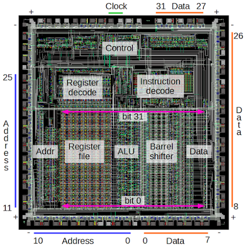
The diagram below shows the most important functional blocks of the ARM chip.[2] The actual processing happens in the bottom half of the chip, which implements the data path. The chip operates on 32 bits at a time so it is structured as 32 horizontal layers: bit 31 at the top, down to bit 0 at the bottom. Several data buses run horizontally to connect different sections of the chip. The large register file, with 25 registers, stands out in the image. The Program Counter (register 15) is on the left of the register file and register 0 is on the right.[3]

The main components of the ARM1 chip. Most of the pins are used for address and data lines; unlabeled pins are various control signals.

The main components of the ARM1 chip. Most of the pins are used for address and data lines; unlabeled pins are various control signals.

Computation takes place in the ALU (arithmetic-logic unit), which is to the right of the registers. The ALU performs 16 different operations (add, add with carry, subtract, logical AND, logical OR, etc.) It takes two 32-bit inputs and produces a 32-bit output. The ALU is described in detail here.[4] To the right of the ALU is the 32-bit barrel shifter. This large component performs a binary shift or rotate operation on its input, and is described in more detail below. At the left is the address circuitry which provides an address to memory through the address pins. At the right data circuitry reads and writes data values to memory.

Above the datapath circuitry is the control circuitry. The control lines run vertically from the control section to the data path circuits below. These signals select registers, tell the ALU what operation to perform, and so forth. The instruction decode circuitry processes each instruction and generates the necessary control signals. The register decode block processes the register select bits in an instruction and generates the control signals to select the desired registers.[5]

The pins

The squares around the outside of the image above are the pads that connect the processor to the outside world. The photo below shows the 84-pin package for the ARM1 processor chip. The gold-plated pins are wired to the pads on the silicon chip inside the package.
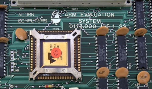
The ARM1 processor chip installed in the Acorn ARM Evaluation System. Original photo by Flibble, https://commons.wikimedia.org/wiki/File:Acorn-ARM-Evaluation-System.jpg, CC BY-SA 3.0.

The ARM1 processor chip installed in the Acorn ARM Evaluation System. Full photo by Flibble, CC BY-SA 3.0.

Most of the pads are used for the address and data lines to memory. The chip has 26 address lines, allowing it to access 64MB of memory, and has 32 data lines, allowing it to read or write 32 bits at a time. The address lines are in the lower left and the data lines are in the lower right. As the simulator runs, you can see the address pins step through memory and the data pins read data from memory. The right hand side of the simulator shows the address and data values in hex, e.g. "A:00000020 D:e1a00271". If you know hex, you can easily match these values to the pin states.

Each corner of the chip has a power pin (+) and a ground pin (-), providing 5 volts to run the chip. Various control signals are at the top of the chip. In the simulator, it is easy to spot the the two clock signals that step the chip through its operations (below). The phase 1 and phase 2 clocks alternate, providing a tick-tock rhythm to the chip. In the simulator, the clock runs at a couple cycles per second, while the real chip has a 8MHz clock, more than a million times faster. Finally, note below the manufacturer's name "ACORN" on the chip in place of pin 82.

The two clock signals for the ARM1 processor chip.

History of the ARM chip

The ARM1 was designed in 1985 by engineers Sophie Wilson (formerly Roger Wilson) and Steve Furber of Acorn Computers. The chip was originally named the Acorn RISC Machine and intended as a coprocessor for the BBC Micro home/educational computer to improve its performance. Only a few hundred ARM1 processors were fabricated, so you might expect ARM to be a forgotten microprocessor, a historical footnote of the 1980s. However, the original ARM1 chip led to the amazingly successful ARM architecture with more than 50 billion ARM chips produced. What happened?

In the early 1980s, academic research suggested that instead of making processor instruction sets more complex, designers would get better performance from a processor that was simple but fast: the Reduced Instruction Set Computer or RISC.[6] The Berkeley and Stanford research papers on RISC inspired the ARM designers to choose a RISC design. In addition, given the small size of the design team at Acorn, a simple RISC chip was a practical choice.[7]

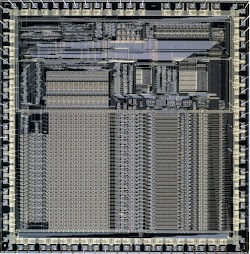
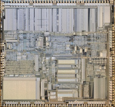
The simplicity of a RISC design is clear when comparing the ARM1 and Intel's 80386, which came out the same year: the ARM1 had about 25,000 transistors versus 275,000 in the 386.[8] The photos below show the two chips at the same scale; the ARM1 is 50mm2 compared to 104mm2 for the 386. (Twenty years later, an ARM7TDMI core was 0.1mm2; magnified at the same scale it would be the size of this square vividly illustrating Moore's law.)

Die photo of the ARM1 processor chip. Courtesy of Computer History Museum. Intel 386 CPU die photo (A80386DX-20). By Pdesousa359, https://commons.wikimedia.org/wiki/File:Intel_A80386DX-20_CPU_Die_Image.jpg (CC BY-SA 3.0)

Die photos of the ARM1 processor and the Intel 386 processor to the same scale. The ARM1 is much smaller and contained 25,000 transistors compared to 275,000 in the 386. The 386 was higher density, with a 1.5 micron process compared to 3 micron for the ARM1. ARM1 photo courtesy of Computer History Museum. Intel A80386DX-20 by Pdesousa359, CC BY-SA 3.0.

Because of the ARM1's small transistor count, the chip used very little power: about 1/10 Watt, compared to nearly 2 Watts for the 386. The combination of high performance and low power consumption made later versions of ARM chip very popular for embedded systems. Apple chose the ARM processor for its ill-fated Newton handheld system and in 1990, Acorn Computers, Apple, and chip manufacturer VLSI Technology formed the company Advanced RISC Machines to continue ARM development.[9]

In the years since then, ARM has become the world's most-used instruction set with more than 50 billion ARM processors manufactured. The majority of mobile devices use an ARM processor; for instance, the Apple A8 processor inside iPhone 6 uses the 64-bit ARMv8-A. Despite its humble beginnings, the ARM1 made IEEE Spectrum's list of 25 microchips that shook the world and PC World's 11 most influential microprocessors of all time.

Looking at the low-level construction of the ARM1 chip

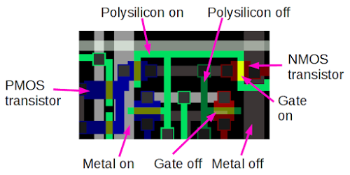
Getting back to the chip itself, the ARM1 chip is constructed from five layers. If you zoom in on the chip in the simulator, you can see the components of the chip, built from these layers. As seen below, the simulator uses a different color for each layer, and highlights circuits that are turned on. The bottom layer is the silicon that makes up the transistors of the chip. During manufacturing, regions of the silicon are modified (doped) by applying different impurities. Silicon can be doped positive to form a PMOS transistor (blue) or doped negative for an NMOS transistor (red). Undoped silicon is basically an insulator (black).

The ARM1 simulator uses different colors to represent the different layers of the chip.

The ARM1 simulator uses different colors to represent the different layers of the chip.

Polysilicon wires (green) are deposited on top of the silicon. When polysilicon crosses doped silicon, it forms the gate of a transistor (yellow). Finally, two layers of metal (gray) are on top of the polysilicon and provide wiring.[10] Black squares are contacts that form connections between the different layers.

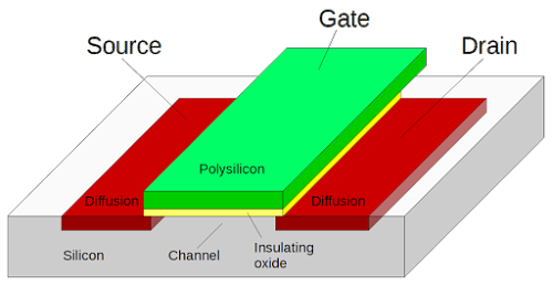
For our purposes, a MOS transistor can be thought of as a switch, controlled by the gate. When it is on (closed), the source and drain silicon regions are connected. When it is off (open), the source and drain are disconnected. The diagram below shows the three-dimensional structure of a MOS transistor.

Structure of a MOS transistor.

Structure of a MOS transistor.

Like most modern processors, the ARM1 was built using CMOS technology, which uses two types of transistors: NMOS and PMOS. NMOS transistors turn on when the gate is high, and pull their output towards ground. PMOS transistors turn on when the gate is low, and pull their output towards +5 volts.

Understanding the register file

The register file is a key component of the ARM1, storing information inside the chip. (As a RISC chip, the ARM1 makes heavy use of its registers.) The register file consists of 25 registers, each holding 32 bits. This section describes step-by-step how the register file is built out of individual transistors.

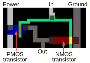
The diagram below shows two transistors forming an inverter. If the input is high (as below), the NMOS transistor (red) turns on, connecting ground to the output so the output is low. If the input is low, the PMOS transistor (blue) turns on, connecting power to the output so the output is high. Thus, the output is the opposite of the input, making an inverter.

An inverter in the ARM1 chip, as displayed by the simulator.

An inverter in the ARM1 chip, as displayed by the simulator.

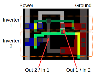
Combining two inverters into a loop forms a simple storage circuit. If the first inverter outputs 1, the second inverter outputs 0, causing the first inverter to output 1, and the circuit is stable. Likewise, if the first inverter outputs 0, the second outputs 1, and the circuit is again stable. Thus, the circuit will remain in either state indefinitely, "remembering" one bit until forced into a different state.

Two inverters in the ARM1 chip form one bit of register storage.

Two inverters in the ARM1 chip form one bit of register storage.

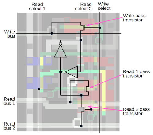
To make this circuit into a useful register cell, read and write bus lines are added, along with select lines to connect the cell to the bus lines. When the write select line is activated, the pass connector connects the write bus to the inverter, allowing a new value to be overwrite the current bit. Likewise, pass transistors connect the bit to a read bus when activated by the corresponding select line, allowing the stored value to be read out.

Schematic of one bit in the ARM1 processor's register file.

Schematic of one bit in the ARM1 processor's register file.

To create the register file, the register cell above is repeated 32 times vertically for each bit, and 25 times horizontally to form each register. Each bit has three horizontal bus lines — the write bus and the two read buses — so there are 32 triples of bus lines. Each register has three vertical control lines — the write select line and two read select lines — so there are 25 triples of control lines. By activating the desired control lines, two registers can be read and one register can be written at a time.[11] When the simulator is running, you can see the vertical control lines activated to select registers, and you can see the data bits flowing on the horizontal bus lines.

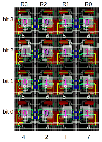
By looking at a memory cell in the simulator, you can see which inverter is on and determine if the bit is a 0 or a 1. The diagram below shows a few register bits. If the upper inverter input is active, the bit is 0; if the lower inverter input is active, the bit is 1. (Look at the green lines above or below the bit values.) Thus, you can read register values right out of the simulator if you look closely.

By looking at the ARM1 register file, you can determine the value of each bit. For a 0 bit, the input to the top inverter is active (green/yellow); for a 1 bit, the input to the bottom inverter is active.

By looking at the ARM1 register file, you can determine the value of each bit. For a 0 bit, the input to the top inverter is active (green/yellow); for a 1 bit, the input to the bottom inverter is active.

The barrel shifter

The barrel shifter, which performs binary shifts, is another interesting component of the ARM1. Most instructions use the barrel shifter, allowing a binary argument to be shifted left, shifted right, or rotated by any amount (0 to 31 bits). While running the simulator, you can see diagonal lines jumping back and forth in the barrel shifter.

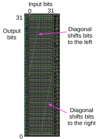
The diagram below shows the structure of the barrel shifter. Bits flows into the shifter vertically with bit 0 on the left and bit 31 on the right. Output bits leave the shifter horizontally with bit 0 on the bottom and bit 31 on top. The diagonal lines visible in the barrel shifter show where the vertical lines are connected to the horizontal lines, generating a shifted output. Different positions of the diagonals result in different shifts. The upper diagonal line shifts bits to the left, and the lower diagonal line shifts bits to the right. For a rotation, both diagonals are active; it may not be immediately obvious but in a rotation part of the word is shifted left and part is shifted right.

Structure of the barrel shifter in the ARM1 chip.

Structure of the barrel shifter in the ARM1 chip.

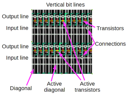
Zooming in on the barrel shifter shows exactly how it works. It contains a 32 by 32 crossbar grid of transistors, each connecting one vertical line to one horizontal line. The transistor gates are connected by diagonal control lines; transistors along the active diagonal connect the appropriate vertical and horizontal lines. Thus, by activating the appropriate diagonals, the output lines are connected to the input lines, shifted by the desired amounts. Since the chip's input lines all run horizontally, there are 32 connections between input lines and the corresponding vertical bit lines.

Details of the barrel shifter in the ARM1 chip. Transistors along a specific diagonal are activated to connect the vertical bit lines and output lines. Each input line is connected to a vertical bit line through the indicated connections.

Details of the barrel shifter in the ARM1 chip. Transistors along a specific diagonal are activated to connect the vertical bit lines and output lines. Each input line is connected to a vertical bit line through the indicated connections.

The demonstration program

When you run the simulator, it executes a short hardcoded program that performs shifts of increasing amounts. You don't need to understand the code, but if you're curious it is:
0000  E1A0100F mov     r1, pc        @ Some setup
0004  E3A0200C mov     r2, #12
0008  E1B0F002 movs    pc, r2
000C  E1A00000 nop
0010  E1A00000 nop
0014  E3A02001 mov     r2, #1        @ Load register r2 with 1
0018  E3A0100F mov     r1, #15       @ Load r1 with value to shift
001C  E59F300C ldr     r3, pointer
    loop:
0020  E1A00271 ror     r0, r1, r2    @ Rotate r1 by r2 bits, store in r0
0024  E2822001 add     r2, r2, #1    @ Add 1 to r2
0028  E4830004 str     r0, [r3], #4  @ Write result to memory
002C  EAFFFFFB b       loop          @ Branch to loop
Inside the loop, register r1 (0x000f) is rotated to the right by r2 bit positions and the result is stored in register r0. Then r2 is incremented and the shift result written to memory. As the simulator runs, watch as r2 is incremented and as r0 goes through the various values of 4 bits rotated. The A and D values show the address and data pins as instructions are read from memory.

The changing shift values are clearly visible in the barrel shifter, as the diagonal line shifts position. If you zoom in on the register file, you can read out the values of the registers, as described earlier.

Conclusion

The ARM1 processor led to the amazingly successful ARM processor architecture that powers your smart phone. The simple RISC architecture of the ARM1 makes the circuitry of the processor easy to understand, at least compared to a chip such as the 386.[12] The ARM1 simulator provides a fascinating look at what happens inside a processor, and hopefully this article has helped explain what you see in the simulator.

P.S. If you want to read more about ARM1 internals, see Dave Mugridge's series of posts:
Inside the armv1 Register Bank
Inside the armv1 Register Bank - register selection
Inside the armv1 Read Bus
Inside the ALU of the armv1 - the first ARM microprocessor

Notes and references

[1] I should make it clear that I am not part of the Visual 6502 team that built the ARM1 simulator. More information on the simulator is in the Visual 6502 team's blog post The Visual ARM1.

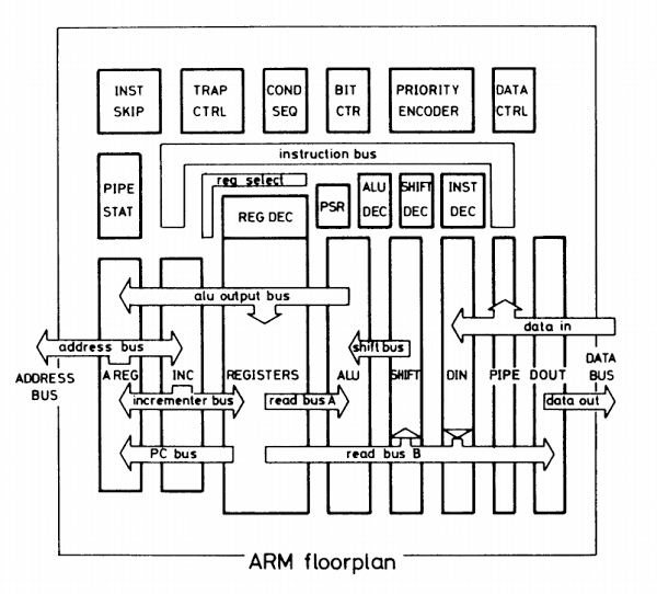
[2] The block diagram below shows the components of the chip in more detail. See the ARM Evaluation System manual for an explanation of each part.

Floorplan of the ARM1 chip, from ARM Evaluation System manual. (Bus labels are corrected from original.)

Floorplan of the ARM1 chip, from ARM Evaluation System manual. (Bus labels are corrected from original.)

[3] You may have noticed that the ARM architecture describes 16 registers, but the chip has 25 physical registers. There are 9 "extra" registers because there are extra copies of some registers for use while handling interrupts.

Another interesting thing about the register file is the PC register is missing a few bits. Since the ARM1 uses 26-bit addresses, the top 6 bits are not used. Because all instructions are aligned on a 32-bit boundary, the bottom two address bits in the PC are always zero. These 8 bits are not only unused, they are omitted from the chip entirely.

[4] The ALU doesn't support multiplication (added in ARM 2) or division (added in ARMv7).

[5] A bit more detail on the decode circuitry. Instruction decoding is done through three separate PLAs. The ALU decode PLA generates control signals for the ALU based on the four operation bits in the instruction. The shift decode PLA generates control signals for the barrel shifter. The instruction decode PLA performs the overall decoding of the instruction. The register decode block consists of three layers. Each layer takes a 4-bit register id and activates the corresponding register. There are three layers because ARM operations use two registers for inputs and a third register for output.

[6] In a RISC computer, the instruction set is restricted to the most-used instructions, which are optimized for high performance and can typically execute in a single clock cycle. Instructions are a fixed size, simplifying the instruction decoding logic. A RISC processor requires much less circuitry for control and instruction decoding, leaving more space on the chip for registers. Most instructions operate on registers, and only load and store instructions access memory. For more information on RISC vs CISC, see RISC architecture.

[7] For details on the history of the ARM1, see Conversation with Steve Furber: The designer of the ARM chip shares lessons on energy-efficient computing.

[8] The 386 and the ARM1 instruction sets are different in many interesting ways. The 386 has instructions from 1 byte to 15 bytes, while all ARM1 instructions are 32-bits long. The 386 has 15 registers - all with special purposes, while the ARM1 has 25 registers, mostly general-purpose. 386 instructions can usually operate on memory, while ARM1 instructions operate on registers except for load and store. The 386 has about 140 different instructions, compared to a couple dozen in the ARM1 (depending how you count). Take a look at the 386 opcode map to see how complex decoding a 386 instruction is. ARM1 instructions fall into 5 categories and can be simply decoded. (I'm not criticizing the 386's architecture, just pointing out the major architectural differences.)

See the Intel 80386 Programmer's Reference Manual and 80386 Hardware Reference Manual for more details on the 386 architecture.

[9] Interestingly the ARM company doesn't manufacture chips. Instead, the ARM intellectual property is licensed to hundreds of different companies that build chips that use the ARM architecture. See The ARM Diaries: How ARM's business model works for information on how ARM makes money from licensing the chip to other companies.

[10] The first metal layer in the chip runs largely top-to-bottom, while the second metal layer runs predominantly horizontally. Having two layers of metal makes the layout much simpler than single-layer processors such as the 6502 or Z-80.

[11] In the register file, alternating bits are mirrored to simplify the layout. This allows neighboring bits to share power and ground lines. The ARM1's register file is triple-ported, so two register can be read and one register written at the same time. This is in contrast to chips such as the 6502 or Z-80, which can only access registers one at a time.

[12] For more information on the ARM1 internals, the book VLSI Risc Architecture and Organization by ARM chip designer Steven Furber has a hundred pages of information on the ARM chip internals. An interesting slide deck is A Brief History of ARM by Lee Smith, ARM Fellow.

Creating high resolution integrated circuit die photos with Hugin or ICE

Have you ever wanted to take a bunch of photos of an integrated circuit die and combine them into a high-res image? The stitching software can be difficult, so I've written a guide to the process I use. These tips may also be useful for other Hugin panoramas.

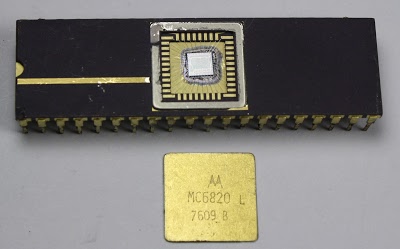
The first step is to take a bunch of photos of the die with a microscope. I used an old Motorola 6820 PIA (Peripheral Interface Adapter) chip. This chip had a metal cap over the die that popped off easily with a chisel, exposing the die. The 6820 is notable as the keyboard interface chip in the Apple I computer.

The MC6820 chip with the metal lid popped off to reveal the silicon die.

The MC6820 chip with the metal lid popped off to reveal the silicon die.

The next step is to take photos of the die through a microscope. I used an AmScope metallurgical microscope like the one below. A metallurgical microscope shines the light from above so you can view opaque objects such as chips. (The box on the right of the microscope is the light.) It's much easier if the microscope has an X-Y stage to precisely move the die for each picture.
The key to success is pictures with substantial overlap, so the software can figure out how to combine them. Use more overlap than you think necessary - at least 30% is good. Skimping on the overlap may result in hours of manual work later. The quality of the input photos is also important - make sure the die is level so you can get sharp focus across the whole image. Give the images structured names according to their grid position: 11.png, 12.png, 21.png, ... This will make it much easier to figure out which photos are overlapping neighbors when stitching them together.

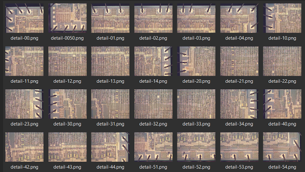
For this article, I used the set of images below. Some of them overlap substantially, and some ... not so much. As a result, this article describes a fairly difficult stitch. In the process I learned the importance of overlap, and Hugin worked much better when I tried again with a denser set of images.
The set of images used to generate the die photo.

The set of images used to generate the die photo.

The easiest way to stitch together photos is with Microsoft's Image Composite Editor (ICE). You simply import the photos, click Stitch, and save the result. If ICE works, it's super-easy, but it doesn't have any flexibility if you run into problems (as I did). ICE can be downloaded from Microsoft.

If ICE doesn't work for you, the open-source Hugin panorama photo stitcher is much more flexible and provides many more options. While Hugin is easy to use for simple panoramas, it's pretty confusing for more complex projects, which is why I've written this. The software can be downloaded from the Hugin website. To start a stitch with Hugin, load the images by dragging-and-dropping them into the Photos window. Enter "Normal (rectilinear)" for the lens type and 1 for HFOV in the dialog.
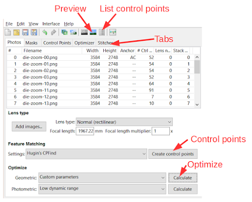
The next step is to generate the control points, which indicate features that match between pairs of images. The control points are what tie the images together, so high quality control points are critical. To generate control points, under "Feature Matching" select "Hugin's CPFind" and click "Create control points". (See the screenshot below.) It will take several minutes to generate control points. You can install other control point finders if you want. Autopano-SIFT-C is said to be good, but I didn't get good results at all with it; it is in a zip file here.

Main screen of the Hugin panorama program

Main screen of the Hugin panorama program

Next, optimize the control points to fit the images together. Select Custom Parameters under Optimize, which will add the Optimizer tab. Go to the Optimize tab, and disable rotation and lens parameter optimization, so only Pitch and Yaw are optimized: Right click on Roll, and select "Unselect all", so the roll entries are not underlined. Do the same for lens parameters. Back at the Photos tab, select "Positions (incremental, starting from anchor)" under Optimize and click "Calculate". Hugin will try to find the best positions for the images. You want a maximum distance of a few pixels, but if you're unlucky the distance may be in the hundreds. Click Yes to apply the optimization.

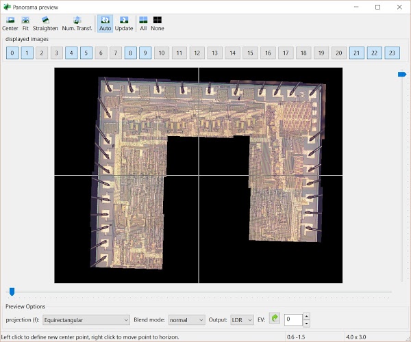
The Panorama Preview icon will generate a panorama based on the control points. To get the image to the center, click Center and then click the center of the images. Click Fit and it may fit the panorama into the window, or you may need to move the sliders (very slowly). Above the panorama, you can select which images you wish to display. Important: only the selected images will be optimized. If you don't have enough images selected, you'll get the mysterious error "No Feature Points". As you can see below, my first attempt was a mess with all the images in one badly-aligned horizontal strip.

An unsuccessful attempt to generate a composite photo of an IC die with Hugin.

An unsuccessful attempt to generate a composite photo of an IC die with Hugin.

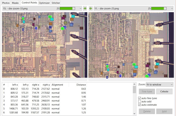
The next step is to fix the control points. Because Hugin optimizes globally, even a few bad control points can mess up the entire image. The main way to fix control points is the Control Points screen, shown below. Select an image on the left and an image on the right. The image selection dialog shows how many control points match between the images. The squares on the images indicate matching control points, which are also listed. If images overlap but don't have any control points, add control points by clicking matching spots in the left and right images. The images will then zoom so you can fine-tune the positions. Finally, click Add.

The control point editing screen in Hugin.

The control point editing screen in Hugin.

A quick way to create control points between two images that overlap is to re-run Hugin's feature mapper on the pair of images. Go to the Photos tab, control-click two images, and then click Create Control Points. If the images overlap sufficiently, Hugin should find control points. If this doesn't work, you're stuck with manually adding points as described above.

If two images shouldn't share control points, go to the Control Points tab, select the two images and delete their control points. This is where organized naming of the images helps - if you see control points between img00 and img35, there's probably something wrong.

You can also clean up bad control points with the control points list. Click the Show Control Points icon at the top and click Distance to sort. You should see a lot of small distances (good) and some very large distances (bad) at the bottom. Click a large distance, and it will bring up the Control Points page. Delete the bad control points. You can also do a bulk delete from the Show Control Points dialog. Click Select by Distance, enter 50 (for example), and then click delete. (But be warned this could delete some good control points too, so you might want to check them first.)

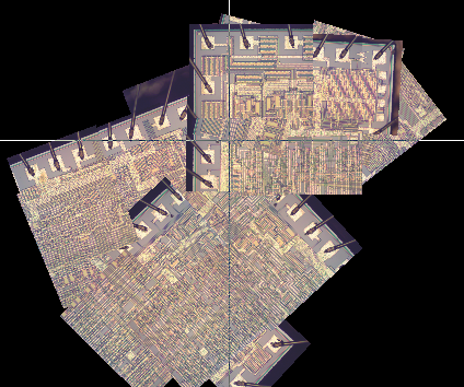
Once the control points are reasonably sensible, go back to the Photos tab and re-optimize. If you're lucky, the images will now be aligned. Unfortunately, I ended up with a cubist mess. I'll explain how to still get a panorama even if you run into problems like this.

Another unsuccessful attempt to make a composite die photo with Hugin.

Another unsuccessful attempt to make a composite die photo with Hugin.

If the parameters get too messed up, select Custom Parameters under Optimize, which will add the Optimizer tab. Under that tab you can reset all the parameters, or parameters for individual images. This is helpful if images start showing up rotated, for instance.

To debug your panorama, you can add images to the panorama one at a time to see which image is causing the problems. Use the Panorama Preview to select the images you want to process. After adding each new image, use the Optimizer tab to optimize the selected images: check "Only use control points between image selected in preview window" and click "Optimize now". If the image shows up in the right spot, all is well. Otherwise, there's something wrong with the last image's control points. Examine its control points under the Control Points tab, and delete any bad matches. (Since integrated circuits often have repeated blocks, it's easy for the matcher to generate convincing but entirely wrong control points.) If the newly-added image doesn't show up at all, it probably lacks any control points linking it with the rest of the images, and got placed at the origin. If the image shows up at an angle, it may have just one control point linking it to another image, letting it swivel around, so add more matching control points. After fixing the image's control points, re-optimize and hopefully it will now be placed correctly. You should be able to correct all the problems by proceeding image by image.

The Panorama Preview window in Hugin. By selecting a subset of the images to tile, control point errors can be corrected one image at a time.

The Panorama Preview window in Hugin. By selecting a subset of the images to tile, control point errors can be corrected one image at a time.

Once you have a good preview, you can generate the final image. Go to the Stitcher tab. Select Equirectangular project. Click Calculate field of view. I recommend starting with a small canvas; it's annoying to wait for a 100 megapixel image and then discover it's a mess. I suggest avoiding cropping; Hugin tends to crop too much, and it's easy to crop later with a tool such as Gimp. Finally, click Stitch, save the project, and wait while the image is generated.

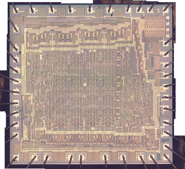
If the result looks good, increase the resolution and generate a high-res version. The photo below shows my final stitched image of the Motorola 6820 die. Click for the full-size image. I've left the image uncropped to make the tiling more visible. I've since made a better composite, starting with source images that overlapped more, and the process was much easier.

Die photo of the Motorola 6820 Peripheral Interface Adapter chip, composited with Hugin.

Die photo of the Motorola 6820 Peripheral Interface Adapter chip, composited with Hugin.

One advanced Hugin feature that may be useful is defining horizontal and vertical lines, so your image comes out straight (wiki). To do this, add control points on a horizontal line between two images, e.g. the upper edge at the left and the upper edge at the right. Note that unlike regular control points, you are not matching the same point in both images, just points on the same horizontal line. After clicking Add, change the mode to Horizontal Line using the dropdown. Put another horizontal edge on the bottom of the die. Vertical lines are similar.

To conclude, making a high-res die photo is an interesting project if you have the right kind of microscope. The Hugin compositing software has a steep learning curve, but hopefully this article will help. Starting with images that overlap significantly will make the process much easier. I should mention that I'm not at all an expert at Hugin or die photos - please leave a comment if you have suggestions.

Acknowledgements: Mikhail at zeptobars gave me helpful advice about Hugin. Other good sites with die photos are Visual 6502 and Silicon Pr0n.

Update: some more advanced information from Mikhail:

Regarding optimizing lens parameters – one of the optimal ways is to make a test panorama, some 10-20 shots with ~50-70% shots overlap. Then you align this (position only, no rotation), and at the end – add lens parameters (first optimize on a,b,c, then d,e then a,b,c,d,e). After that you can export lens distortion calibration data to a file and preload it for a large optimization job, so that you won’t need to optimize it. This works for the same lens and same microscope alignment. Good microscope lenses might be okay without lens correction though.

Another large topic is chromatic aberration correction on individual photos before stitching, which also could be done by Hugin tools.

"c:\Program Files\Hugin\bin\tca_correct.exe" -o cv -n 1000 -t 10 -m 1 5xsample.tif

This will try to detect optimal chromatic aberration correction for a single photo. It will give you coefficients, which could be tested by:

"c:\Program Files\Hugin\bin\fulla.exe" -r 0.0000094:0.0000000:0.0000097:0.9853381 -b -0.0000853:0.0000000:-0.0004039:1.0021658 -s -t 4 -o corrected.tif 5xsample.tif

If corrected looks better than original – you can do that for all photos in a batch before stitching. Each lens needs its own correction batch. So for example I have separate batches for 10x and 20x lenses. 5x lenses is quite good without chroma correction.

set path=%path%;"c:\Program Files\ImageMagick-6.8.7-Q16";"c:\Program Files\Hugin\bin\";
cd image
rem mogrify -shave 3
FOR %%I IN (*.tif) DO "fulla.exe" -r 0.0000000:0.0000000:-0.0003093:0.9990635 -b 0.0000000:0.0000000:0.0016437:1.0004672 -s -t 4 %%I -o %%I
mogrify -crop 4084x3276+6+5 *.tif
rem Original size: 4096x3286
ImageMagick crop is used at the end to cut any warped edges of the frame. Also some Chinese cameras have 1px artifacts on the very edges of the frame that should be cropped.

Macbook charger teardown: The surprising complexity inside Apple's power adapter

Have you ever wondered what's inside your Macbook's charger? There's a lot more circuitry crammed into the compact power adapter than you'd expect, including a microprocessor. This charger teardown looks at the numerous components in the charger and explains how they work together to power your laptop.

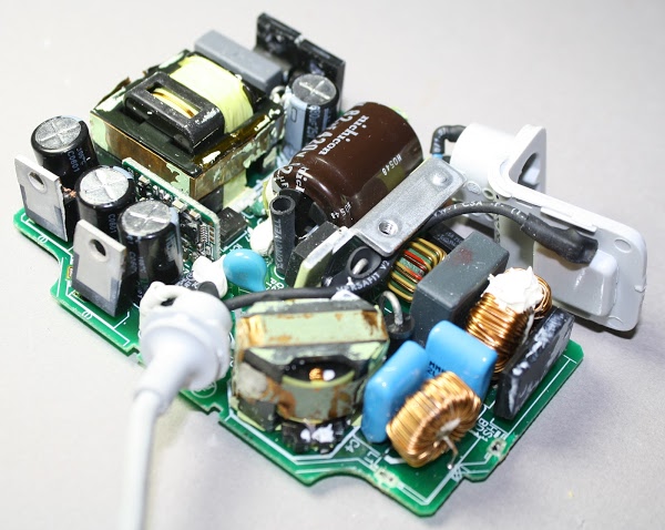
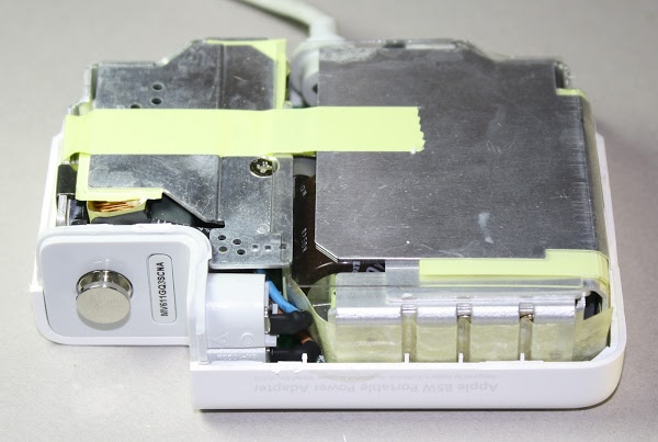
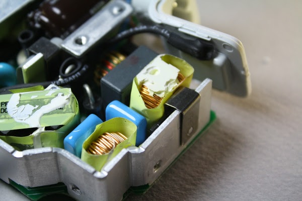
Inside the Macbook charger, after removing the heat sinks and insulating tape.

Inside the Macbook charger. Many electronic components work together to provide smooth power to your laptop.
Most consumer electronics, from your cell phone to your television, use a switching power supply to convert AC power from the wall to the low-voltage DC used by electronic circuits. The switching power supply gets its name because it switches power on and off thousands of times a second, which turns out to be a very efficient way to do this conversion.[1]

Switching power supplies are now very cheap, but this wasn't always the case. In the 1950s, switching power supplies were complex and expensive, used in aerospace and satellite applications that needed small, lightweight power supplies. By the early 1970s, new high-voltage transistors and other technology improvements made switching power supplies much cheaper and they became widely used in computers.[2] The introduction of a single-chip power supply controller in 1976 made switching power supplies simpler, smaller, and cheaper.

Apple's involvement with switching power supplies goes back to 1977 when Apple's chief engineer Rod Holt designed a switching power supply for the Apple II. According to Steve Jobs:[3]

"That switching power supply was as revolutionary as the Apple II logic board was. Rod doesn't get a lot of credit for this in the history books but he should. Every computer now uses switching power supplies, and they all rip off Rod Holt's design."

This is a fantastic quote, but unfortunately it is entirely false. The switching power supply revolution happened before Apple came along, Apple's design was similar to earlier power supplies[4] and other computers don't use Rod Holt's design. Nevertheless, Apple has extensively used switching power supplies and pushes the limits of charger design with their compact, stylish and advanced chargers.

Inside the charger

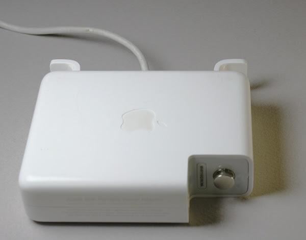
For the teardown I started with a Macbook 85W power supply, model A1172, which is small enough to hold in your palm. The picture below shows several features that can help distinguish the charger from counterfeits: the Apple logo in the case, the metal (not plastic) ground pin on the right, and the serial number next to the ground pin.

Apple 85W Macbook charger

Apple 85W Macbook charger
Strange as it seems, the best technique I've found for opening a charger is to pound on a wood chisel all around the seam to crack it open. With the case opened, the metal heat sinks of the charger are visible. The heat sinks help cool the high-power semiconductors inside the charger.

Inside the Apple 85W Macbook charger

Inside the Apple 85W Macbook charger
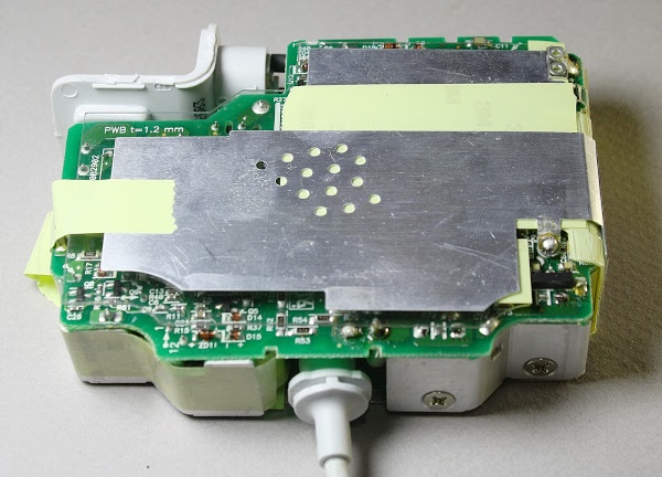
The other side of the charger shows the circuit board, with the power output at the bottom. Some of the tiny components are visible, but most of the circuitry is covered by the metal heat sink, held in place by yellow insulating tape.

The circuit board inside the Apple 85W Macbook charger.

The circuit board inside the Apple 85W Macbook charger. At the right, screws firmly attach components to the heat sinks.
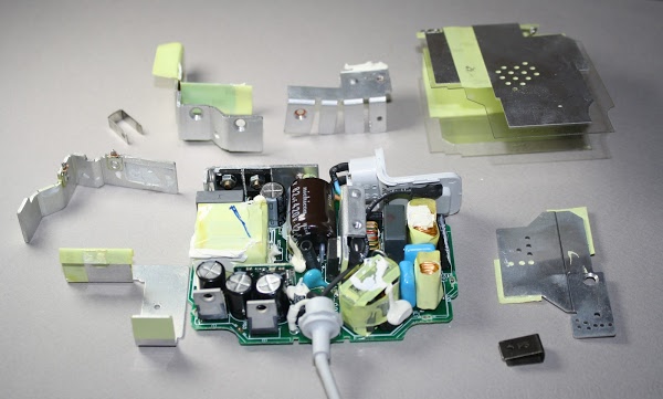
After removing the metal heat sinks, the components of the charger are visible. These metal pieces give the charger a substantial heft, more than you'd expect from a small unit.

Exploded view of the Apple 85W charger

Exploded view of the Apple 85W charger, showing the extensive metal heat sinks.
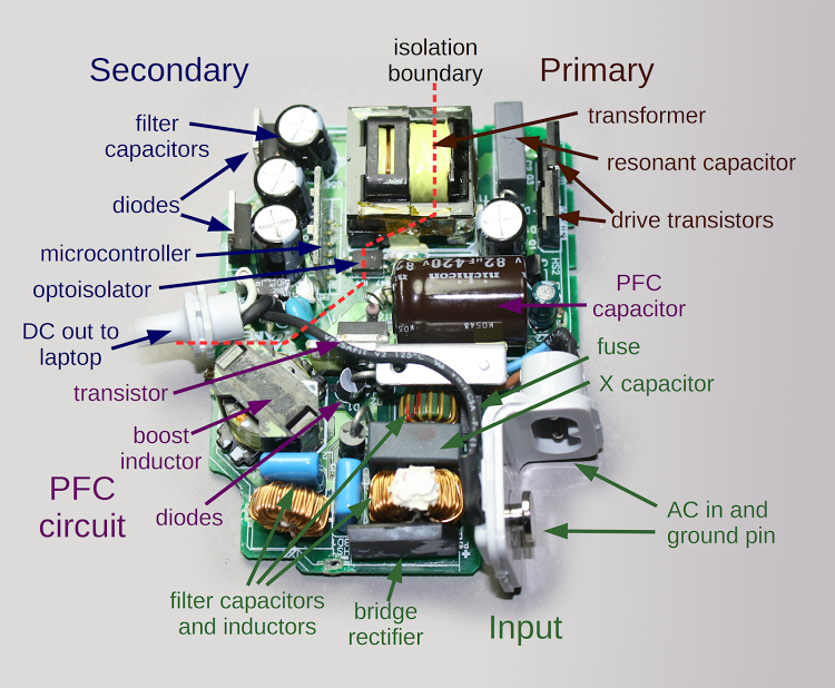
The diagram below labels the main components of the charger. AC power enters the charger and is converted to DC. The PFC circuit (Power Factor Correction) improves efficiency by ensuring the load on the AC line is steady. The primary chops up the high-voltage DC from the PFC circuit and feeds it into the transformer. Finally, the secondary receives low-voltage power from the transformer and outputs smooth DC to the laptop. The next few sections discuss these circuits in more detail, so follow along with the diagram below.

The components inside an Apple Macbook 85W power supply.

The components inside an Apple Macbook 85W power supply.

AC enters the charger

AC power enters the charger through a removable AC plug. A big advantage of switching power supplies is they can be designed to run on a wide range of input voltages. By simply swapping the plug, the charger can be used in any region of the world, from European 240 volts at 50 Hertz to North American 120 volts at 60 Hz. The filter capacitors and inductors in the input stage prevent interference from exiting the charger through the power lines. The bridge rectifier contains four diodes, which convert the AC power into DC. (See this video for a great demonstration of how a full bridge rectifier works.)

The input filtering in a Macbook charger. The diode bridge is attached to the metal heat sink with a clip.

The input components in a Macbook charger. The diode bridge rectifier is attached to the metal heat sink with a clip.

PFC: smoothing the power usage

The next step in the charger's operation is the Power Factor Correction circuit (PFC), labeled in purple. One problem with simple chargers is they only draw power during a small part of the AC cycle.[5] If too many devices do this, it causes problems for the power company. Regulations require larger chargers to use a technique called power factor correction so they use power more evenly.

The PFC circuit uses a power transistor to precisely chop up the input AC tens of thousands of times a second; contrary to what you might expect, this makes the load on the AC line smoother. Two of the largest components in the charger are the inductor and PFC capacitor that help boost the voltage to about 380 volts DC.[6]

The primary: chopping up the power

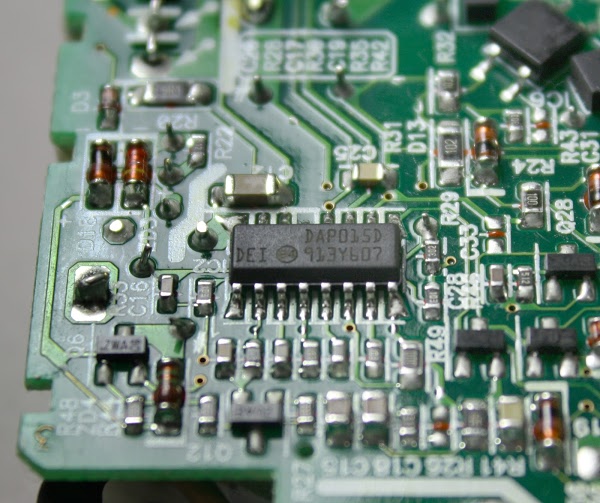
The primary circuit is the heart of the charger. It takes the high voltage DC from the PFC circuit, chops it up and feeds it into the transformer to generate the charger's low-voltage output (16.5-18.5 volts). The charger uses an advanced design called a resonant controller, which lets the system operate at a very high frequency, up to 500 kilohertz. The higher frequency permits smaller components to be used for a more compact charger. The chip below controls the switching power supply.[7]

The circuit board inside the Macbook charger. The chip in the middle controls the switching power supply circuit.

The circuit board inside the Macbook charger. The chip in the middle controls the switching power supply circuit.

The two drive transistors (in the overview diagram) alternately switch on and off to chop up the input voltage. The transformer and capacitor resonate at this frequency, smoothing the chopped-up input into a sine wave.

The secondary: smooth, clean power output

The secondary side of the circuit generates the output of the charger. The secondary receives power from the transformer and converts it DC with diodes. The filter capacitors smooth out the power, which leaves the charger through the output cable.

The most important role of the secondary is to keep the dangerous high voltages in the rest of the charger away from the output, to avoid potentially fatal shocks. The isolation boundary marked in red on the earlier diagram indicates the separation between the high-voltage primary and the low-voltage secondary. The two sides are separated by a distance of about 6 mm, and only special components can cross this boundary.

The transformer safely transmits power between the primary and the secondary by using magnetic fields instead of a direct electrical connection. The coils of wire inside the transformer are triple-insulated for safety. Cheap counterfeit chargers usually skimp on the insulation, posing a safety hazard. The optoisolator uses an internal beam of light to transmit a feedback signal between the secondary and primary. The control chip on the primary side uses this feedback signal to adjust the switching frequency to keep the output voltage stable.

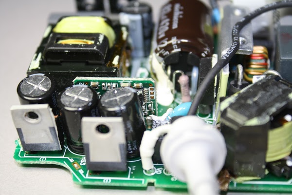
The output components in an Apple Macbook charger. The microcontroller board is visible behind the capacitors.

The output components in an Apple Macbook charger.The two power diodes are in front on the left. Behind them are three cylindrical filter capacitors.The microcontroller board is visible behind the capacitors.

A powerful microprocessor in your charger?

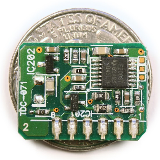
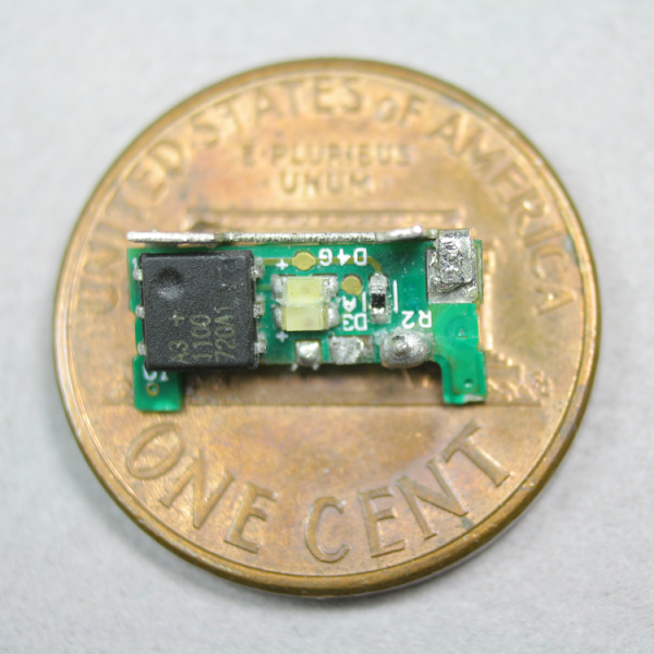
One unexpected component is a tiny circuit board with a microcontroller, which can be seen above. This 16-bit processor constantly monitors the charger's voltage and current. It enables the output when the charger is connected to a Macbook, disables the output when the charger is disconnected, and shuts the charger off if there is a problem. This processor is a Texas Instruments MSP430 microcontroller, roughly as powerful as the processor inside the original Macintosh.[8]

The microcontroller circuit board from an 85W Macbook power supply, on top of a quarter. The MPS430 processor monitors the charger's voltage and current.

The microcontroller circuit board from an 85W Macbook power supply, on top of a quarter. The MPS430 processor monitors the charger's voltage and current.

The square orange pads on the right are used to program software into the chip's flash memory during manufacturing.[9] The three-pin chip on the left (IC202) reduces the charger's 16.5 volts to the 3.3 volts required by the processor.[10]

The charger's underside: many tiny components

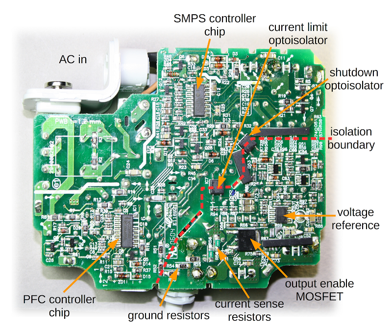
Turning the charger over reveals dozens of tiny components on the circuit board. The PFC controller chip and the power supply (SMPS) controller chip are the main integrated circuits controlling the charger. The voltage reference chip is responsible for keeping the voltage stable even as the temperature changes.[11] These chips are surrounded by tiny resistors, capacitors, diodes and other components. The output MOSFET transistor switches the power to the output on and off, as directed by the microcontroller. To the left of it, the current sense resistors measure the current flowing to the laptop.

The printed circuit board from an Apple 85W Macbook power supply, showing the tiny components inside the charger.

The printed circuit board from an Apple 85W Macbook power supply, showing the tiny components inside the charger.
The isolation boundary (marked in red) separates the high voltage circuitry from the low voltage output components for safety. The dashed red line shows the isolation boundary that separates the low-voltage side (bottom right) from the high-voltage side. The optoisolators send control signals from the secondary side to the primary, shutting down the charger if there is a malfunction.[12]

One reason the charger has more control components than a typical charger is its variable output voltage. To produce 60 watts, the charger provides 16.5 volts at 3.6 amps. For 85 watts, the voltage increases to 18.5 volts at 4.6 amps. This allows the charger to be compatible with lower-voltage 60 watt chargers, while still providing 85 watts for laptops that can use it.[13] As the current increases above 3.6 amps, the circuit gradually increases the output voltage. If the current increases too much, the charger abruptly shuts down around 90 watts.[14]

Inside the Magsafe connector

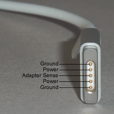
The magnetic Magsafe connector that plugs into the Macbook is more complex than you would expect. It has five spring-loaded pins (known as Pogo pins) to connect to the laptop. Two pins are power, two pins are ground, and the middle pin is a data connection to the laptop.

The pins of a Magsafe 2 connector. The pins are arranged symmetrically, so the connector can be plugged in either way.

The pins of a Magsafe 2 connector. The pins are arranged symmetrically, so the connector can be plugged in either way.
Inside the Magsafe connector is a tiny chip that informs the laptop of the charger's serial number, type, and power. The laptop uses this data to determine if the charger is valid. This chip also controls the status LEDs. There is no data connection to the charger block itself; the data connection is only with the chip inside the connector. For more details, see my article on the Magsafe connector.

The circuit board inside a Magsafe connector is very small. There are two LEDs on each side. The chip is a DS2413 1-Wire switch.

The circuit board inside a Magsafe connector is very small. There are two LEDs on each side. The chip is a DS2413 1-Wire switch.

Operation of the charger

You may have noticed that when you plug the connector into a Macbook, it takes a second or two for the LED to light up. During this time, there are complex interactions between the Macbook, the charger, and the Magsafe connector.

When the charger is disconnected from the laptop, the output transistor discussed earlier blocks the output power.[15] When the Magsafe connector is plugged into a Macbook, the laptop pulls the power line low.[16] The microcontroller in the charger detects this and after exactly one second enables the power output. The laptop then loads the charger information from the Magsafe connector chip. If all is well, the laptop starts pulling power from the charger and sends a command through the data pin to light the appropriate connector LED. When the Magsafe connector is unplugged from the laptop, the microcontroller detects the loss of current flow and shuts off the power, which also extinguishes the LEDs.

You might wonder why the Apple charger has all this complexity. Other laptop chargers simply provide 16 volts and when you plug it in, the computer uses the power. The main reason is for safety, to ensure that power isn't flowing until the connector is firmly attached to the laptop. This minimizes the risk of sparks or arcing while the Magsafe connector is being put into position.

Why you shouldn't get a cheap charger

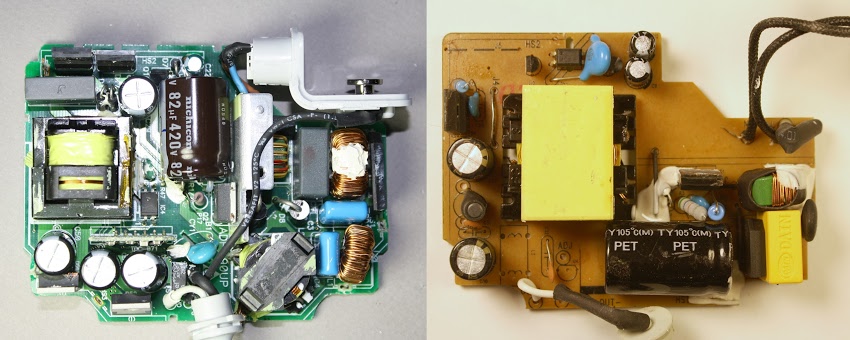
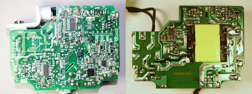
The Macbook 85W charger costs $79 from Apple, but for $14 you can get a charger on eBay that looks identical. Do you get anything for the extra $65? I opened up an imitation Macbook charger to see how it compares with the genuine charger. From the outside, the charger looks just like an 85W Apple charger except it lacks the Apple name and logo. But looking inside reveals big differences. The photos below show the genuine Apple charger on the left and the imitation on the right.

Inside the Apple 85W Macbook charger (left) vs an imitation charger (right). The genuine charger is crammed full of components, while the imitation has fewer parts.

Inside the Apple 85W Macbook charger (left) vs an imitation charger (right). The genuine charger is crammed full of components, while the imitation has fewer parts.

The imitation charger has about half the components of the genuine charger and a lot of blank space on the circuit board. While the genuine Apple charger is crammed full of components, the imitation leaves out a lot of filtering and regulation as well as the entire PFC circuit. The transformer in the imitation charger (big yellow rectangle) is much bulkier than in Apple's charger; the higher frequency of Apple's more advanced resonant converter allows a smaller transformer to be used.

The circuit board of the Apple 85W Macbook charger (left) compared with an imitation charger (right). The genuine charger has many more components.

The circuit board of the Apple 85W Macbook charger (left) compared with an imitation charger (right). The genuine charger has many more components.

Flipping the chargers over and looking at the circuit boards shows the much more complex circuitry of the Apple charger. The imitation charger has just one control IC (in the upper left).[17] since the PFC circuit is omitted entirely. In addition, the control circuits are much less complex and the imitation leaves out the ground connection.

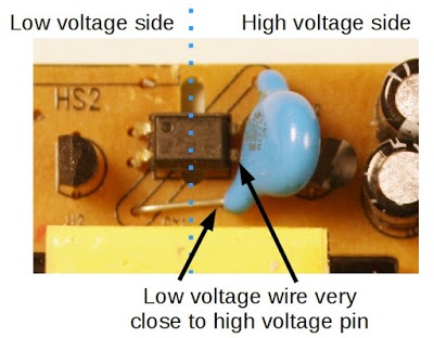
The imitation charger is actually better quality than I expected, compared to the awful counterfeit iPad charger and iPhone charger that I examined. The imitation Macbook charger didn't cut every corner possible and uses a moderately complex circuit. The imitation charger pays attention to safety, using insulating tape and keeping low and high voltages widely separated, except for one dangerous assembly error that can be seen below. The Y capacitor (blue) was installed crooked, so its connection lead from the low-voltage side ended up dangerously close to a pin on the high-voltage side of the optoisolator (black), creating a risk of shock.

Safety hazard inside an imitation Macbook charger. The lead of the Y capacitor is too close to the pin of the optoisolator, causing a risk of shock.

Safety hazard inside an imitation Macbook charger. The lead of the Y capacitor is too close to the pin of the optoisolator, causing a risk of shock.

Problems with Apple's chargers

The ironic thing about the Apple Macbook charger is that despite its complexity and attention to detail, it's not a reliable charger. When I told people I was doing a charger teardown, I rapidly collected a pile of broken chargers from people who had failed chargers. The charger cable is rather flimsy, leading to a class action lawsuit stating that the power adapter dangerously frays, sparks and prematurely fails to work. Apple provides detailed instructions on how to avoid damaging the wire, but a stronger cable would be a better solution. The result is reviews on the Apple website give the charger a dismal 1.5 out of 5 stars.

Burn mark inside an 85W Apple Macbook power supply that failed.

Burn mark inside an 85W Apple Macbook power supply that failed.

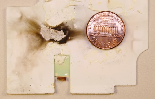
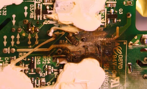
Macbook chargers also fail due to internal problems. The photos above and below show burn marks inside a failed Apple charger from my collection.[18] I can't tell exactly what went wrong, but something caused a short circuit that burnt up a few components. (The white gunk in the photo is insulating silicone used to mount the board.)

Burn marks inside an Apple Macbook charger that malfunctioned.

Burn marks inside an Apple Macbook charger that malfunctioned.

Why Apple's chargers are so expensive

As you can see, the genuine Apple charger has a much more advanced design than the imitation charger and includes more safety features. However, the genuine charger costs $65 more and I doubt the additional components cost more than $10 to $15[19]. Most of the cost of the charger goes into the healthy profit margin that Apple has on their products. Apple has an estimated 45% profit margin on iPhones[20] and chargers are probably even more profitable. Despite this, I don't recommend saving money with a cheap eBay charger due to the safety risk.

Conclusion

People don't give much thought to what's inside a charger, but a lot of interesting circuitry is crammed inside. The charger uses advanced techniques such as power factor correction and a resonant switching power supply to produce 85 watts of power in a compact, efficient unit. The Macbook charger is an impressive piece of engineering, even if it's not as reliable as you'd hope. On the other hand, cheap no-name chargers cut corners and often have safety issues, making them risky, both to you and your computer.

Notes and references

[1] The main alternative to a switching power supply is a linear power supply, which is much simpler and converts excess voltage to heat. Because of this wasted energy, linear power supplies are only about 60% efficient, compared to about 85% for a switching power supply. Linear power supplies also use a bulky transformer that may weigh multiple pounds, while switching power supplies can use a tiny high-frequency transformer.

[2] Switching power supplies were taking over the computer industry as early as 1971. Electronics World said that companies using switching regulators "read like a 'Who's Who' of the computer industry: IBM, Honeywell, Univac, DEC, Burroughs, and RCA, to name a few". See "The Switching Regulator Power Supply", Electronics World v86 October 1971, p43-47. In 1976, Silicon General introduced SG1524 PWM integrated circuit, which put the control circuitry for a switching power supply on a single chip.

[3] The quote about the Apple II power supply is from page 74 of the 2011 book Steve Jobs by Walter Isaacson. It inspired me to write a detailed history of switching power supplies: Apple didn't revolutionize power supplies; new transistors did. Steve Job's quote sounds convincing, but I consider it the reality distortion field in effect.

[4] If anyone can take the credit for making switching power supplies an inexpensive everyday product, it is Robert Boschert. He started selling switching power supplies in 1974 for everything from printers and computers to the F-14 fighter plane. See Robert Boschert: A Man Of Many Hats Changes The World Of Power Supplies in Electronic Design. The Apple II's power supply is very similar to the Boschert OL25 flyback power supply but with a patented variation.

[5] You might expect the bad power factor is because switching power supplies rapidly turn on and off, but that's not the problem. The difficulty comes from the nonlinear diode bridge, which charges the input capacitor only at peaks of the AC signal. (If you're familiar with power factors due to phase shift, this is totally different. The problem is the non-sinusoidal current, not a phase shift.)

The idea behind PFC is to use a DC-DC boost converter before the switching power supply itself. The boost converter is carefully controlled so its input current is a sinusoid proportional to the AC waveform. The result is the boost converter looks like a nice resistive load to the power line, and the boost converter supplies steady voltage to the switching power supply components.

[6] The charger uses a MC33368 "High Voltage GreenLine Power Factor Controller" chip to run the PFC. The chip is designed for low power, high-density applications so it's a good match for the charger.

[7] The SMPS controller chip is a L6599 high-voltage resonant controller; for some reason it is labeled DAP015D. It uses a resonant half-bridge topology; in a half-bridge circuit, two transistors control power through the transformer first one direction and then the other. Common switching power supplies use a PWM (pulse width modulation) controller, which adjusts the time the input is on. The L6599, on the other hand, adjusts the frequency instead of the pulse width. The two transistors alternate switching on for 50% of the time. As the frequency increases above the resonant frequency, the power drops, so controlling the frequency regulates the output voltage.

[8] The processor in the charger is a MSP430F2003 ultra low power microcontroller with 1kB of flash and just 128 bytes of RAM. It includes a high-precision 16-bit analog to digital converter. More information is here.

The 68000 microprocessor from the original Apple Macintosh and the 430 microcontroller in the charger aren't directly comparable as they have very different designs and instruction sets. But for a rough comparison, the 68000 is a 16/32 bit processor running at 7.8MHz, while the MSP430 is a 16 bit processor running at 16MHz. The Dhrystone benchmark measures 1.4 MIPS (million instructions per second) for the 68000 and much higher performance of 4.6 MIPS for the MSP430. The MSP430 is designed for low power consumption, using about 1% of the power of the 68000.

[9] The 60W Macbook charger uses a custom MSP430 processor, but the 85W charger uses a general-purpose processor that needs to loaded with firmware. The chip is programmed with the Spy-Bi-Wire interface, which is TI's two-wire variant of the standard JTAG interface. After programming, a security fuse inside the chip is blown to prevent anyone from reading or modifying the firmware.

[10] The voltage to the processor is provided by not by a standard voltage regulator, but a LT1460 precision reference, which outputs 3.3 volts with the exceptionally high accuracy of 0.075%. This seems like overkill to me; this chip is the second-most expensive chip in the charger after the SMPS controller, based on Octopart's prices.

[11] The voltage reference chip is unusual, it is a TSM103/A that combines two op amps and a 2.5V reference in a single chip. Semiconductor properties vary widely with temperature, so keeping the voltage stable isn't straightforward. A clever circuit called a bandgap reference cancels out temperature variations; I explain it in detail here.

[12] Since some readers are very interested in grounding, I'll give more details. A 1KΩ ground resistor connects the AC ground pin to the charger's output ground. (With the 2-pin plug, the AC ground pin is not connected.) Four 9.1MΩ resistors connect the internal DC ground to the output ground. Since they cross the isolation boundary, safety is an issue. Their high resistance avoids a shock hazard. In addition, since there are four resistors in series for redundancy, the charger remains safe even if a resistor shorts out somehow. There is also a Y capacitor (680pF, 250V) between the internal ground and output ground; this blue capacitor is on the upper side of the board. A T5A fuse (5 amps) protects the output ground.

[13] The power in watts is simply the volts multiplied by the amps. Increasing the voltage is beneficial because it allows higher wattage; the maximum current is limited by the wire size.

[14] The control circuitry is fairly complex. The output voltage is monitored by an op amp in the TSM103/A chip which compares it with a reference voltage generated by the same chip. This amplifier sends a feedback signal via an optoisolator to the SMPS control chip on the primary side. If the voltage is too high, the feedback signal lowers the voltage and vice versa. That part is normal for a power supply, but ramping the voltage from 16.5 volts to 18.5 volts is where things get complicated.

The output current creates a voltage across the current sense resistors, which have a tiny resistance of 0.005Ω each - they are more like wires than resistors. An op amp in the TSM103/A chip amplifies this voltage. This signal goes to tiny TS321 op amp which starts ramping up when the signal corresponds to 4.1A. This signal goes into the previously-described monitoring circuit, increasing the output voltage.

The current signal also goes into a tiny TS391 comparator, which sends a signal to the primary through another optoisolator to cut the output voltage. This appears to be a protection circuit if the current gets too high. The circuit board has a few spots where zero-ohm resistors (i.e. jumpers) can be installed to change the op amp's amplification. This allows the amplification to be adjusted for accuracy during manufacture.

[15] If you measure the voltage from a Macbook charger, you'll find about six volts instead of the 16.5 volts you'd expect. The reason is the output is deactivated and you're only measuring the voltage through the bypass resistor just below the output transistor.

[16] The laptop pulls the charger output low with a 39.41KΩ resistor to indicate that it is ready for power. An interesting thing is it won't work to pull the output too low - shorting the output to ground doesn't work. This provides a safety feature. Accidental contact with the pins is unlikely to pull the output to the right level, so the charger is unlikely to energize except when properly connected.

[17] The imitation charger uses the Fairchild FAN7602 Green PWM Controller chip, which is more advanced than I expected in a knock-off; I wouldn't have been surprised if it just used a simple transistor oscillator. Another thing to note is the imitation charger uses a single-sided circuit board, while the genuine uses a double-sided circuit board, due to the much more complex circuit.

[18] The burnt charger is an Apple A1222 85W Macbook charger, which is a different model from the A1172 charger in the rest of the teardown. The A1222 is in a slightly smaller, square case and has a totally different design based on the NCP 1203 PWM controller chip. Components in the A1222 charger are packed even more tightly than in the A1172 charger. Based on the burnt-up charger, I think they pushed the density a bit too far.

[19] I looked up many of the charger components on Octopart to see their prices. Apple's prices should be considerably lower. The charger has many tiny resistors, capacitors and transistors; they cost less than a cent each. The larger power semiconductors, capacitors and inductors cost considerably more. I was surprised that the 16-bit MSP430 processor costs only about $0.45. I estimated the price of the custom transformers. The list below shows the main components.

ComponentCost
MSP430F2003 processor$0.45
MC33368D PFC chip$0.50
L6599 controller chip$1.62
LT1460 3.3V reference$1.46
TSM103/A reference$0.16
2x P11NM60AFP 11A 600V MOSFET$2.00
3x Vishay optocoupler$0.48
2x 630V 0.47uF film capacitor$0.88
4x 25V 680uF electrolytic capacitor$0.12
420V 82uF electrolytic capacitor$0.93
polypropylene X2 capacitor$0.17
3x toroidal inductor$0.75
4A 600V diode bridge$0.40
2x dual common-cathode schottky rectifier 60V, 15A$0.80
20NC603 power MOSFET$1.57
transformer$1.50?
PFC inductor$1.50?

[20] The article Breaking down the full $650 cost of the iPhone 5 describes Apple's profit margins in detail, estimating 45% profit margin on the iPhone. Some people have suggested that Apple's research and development expenses explain the high cost of their chargers, but the math shows R&D costs must be negligible. The book Practical Switching Power Supply Design estimates 9 worker-months to design and perfect a switching power supply, so perhaps $200,000 of engineering cost. More than 20 million Macbooks are sold per year, so the R&D cost per charger would be one cent. Even assuming the Macbook charger requires ten times the development of a standard power supply only increases the cost to 10 cents.

Understanding silicon circuits: inside the ubiquitous 741 op amp

The 741 op amp is one of the most famous and popular ICs[1] with hundreds of millions sold since its invention in 1968 by famous IC designer Dave Fullagar. In this article, I look at the silicon die for the 741, discuss how it works, and explain how circuits are built from silicon.

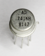
The 741 op amp, packaged in a TO-99 metal can.

The 741 op amp, packaged in a TO-99 metal can.

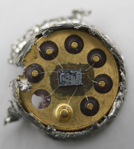
I started with a 741 op amp that was packaged in a metal can (above). Cutting the top off with a hacksaw reveals the tiny silicon die (below), connected to the pins by fine wires.

Inside a 741 op amp, showing the die. This is a TO-99 metal can package, with the top sawed off

Inside a 741 op amp, showing the die. This is a TO-99 metal can package, with the top sawed off

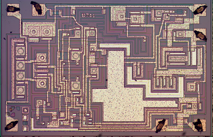
Under a microscope, the details of the silicon chip are visible, as shown below. At first, the chip looks like an incomprehensible maze, but this article will show how transistors, resistors and capacitors are formed on the chip, and explain how they combine to make the op amp.

Die photo of the 741 op amp

Die photo of the 741 op amp

Why op amps are important

Op amps are a key component in analog circuits. An op amp takes two input voltages, subtracts them, multiplies the difference by a huge value (100,000 or more), and outputs the result as a voltage. If you've studied analog circuits, op amps will be familiar to you, but otherwise this may seem like a bizarre and pointless device. How often do you need to subtract two voltages? And why amplify by such a huge factor: will a 1 volt input result in lightning shooting from the op amp? The answer is feedback: by using a feedback signal, the output becomes a sensible value and the high amplification makes the circuit performance stable.

Op amps are used as amplifiers, filters, integrators, differentiators, and many other circuits.[2] Op amps are all around you: your computer's power supply uses op amps for regulation. Your cell phone uses op amps for filtering and amplifying audio signals, camera signals, and the broadcast cell signal.

The structure of the integrated circuit

NPN transistors inside the IC

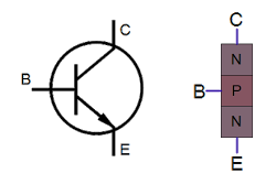
Transistors are the key components in a chip. If you've studied electronics, you've probably seen a diagram of a NPN transistor like the one below, showing the collector (C), base (B), and emitter (E) of the transistor, The transistor is illustrated as a sandwich of P silicon in between two symmetric layers of N silicon; the N-P-N layers make a NPN transistor. It turns out that transistors on a chip look nothing like this, and the base often isn't even in the middle!

Symbol and oversimplified structure of an NPN transistor.

Symbol and oversimplified structure of an NPN transistor.

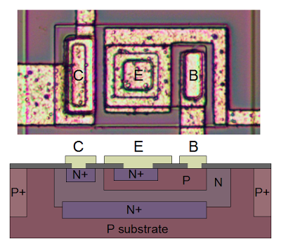
The photo below shows one of the transistors in the 741 as it appears on the chip. The different brown and purple colors are regions of silicon that has been doped differently, forming N and P regions. The whitish-yellow areas are the metal layer of the chip on top of the silicon - these form the wires connecting to the collector, emitter, and base.

Underneath the photo is a cross-section drawing showing approximately how the transistor is constructed. There's a lot more than just the N-P-N sandwich you see in books, but if you look carefully at the vertical cross section below the 'E', you can find the N-P-N that forms the transistor. The emitter (E) wire is connected to N+ silicon. Below that is a P layer connected to the base contact (B). And below that is a N+ layer connected (indirectly) to the collector (C).[3] The transistor is surrounded by a P+ ring that isolates it from neighboring components.

Structure of a NPN transistor in the 741 op amp

Structure of a NPN transistor in the 741 op amp

PNP transistors inside the IC

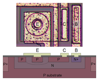
You might expect PNP transistors to be similar to NPN transistors, just swapping the roles of N and P silicon. But for a variety of reasons, PNP transistors have an entirely different construction. They consist of a circular emitter (P), surrounded by a ring shaped base (N), which is surrounded by the collector (P).[4] This forms a P-N-P sandwich horizontally (laterally), unlike the vertical structure of the NPN transistors.

The diagram below shows one of the PNP transistors in the 741, along with a cross-section showing the silicon structure. Note that although the metal contact for the base is on the edge of the transistor, it is electrically connected through the N and N+ regions to its active ring in between the collector and emitter.

Structure of a PNP transistor in the 741 op amp.

Structure of a PNP transistor in the 741 op amp.

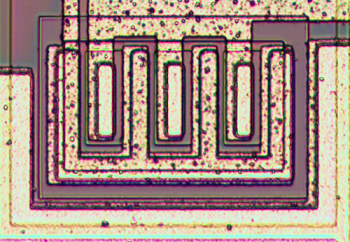
The output transistors in the 741 are larger than the other transistors and have a different structure in order to produce the high-current output. The output transistors must support 25mA, compared to microamps for the internal transistors. The photo below shows one of the output transistors. Note the multiple interlocking "fingers" of the emitter and base, surrounded by the large collector.

A high-current PNP transistor inside the 741 op amp

A high-current PNP transistor inside the 741 op amp

How resistors are implemented in silicon

Resistors are a key component of analog chips. Unfortunately, resistors in ICs are very inaccurate; the resistances can vary by 50% from chip to chip. Thus, analog ICs are designed so only the ratio of resistors matters, not the absolute values, since the ratios remain nearly constant from chip to chip.

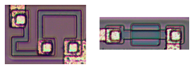
The photo below shows two resistors in the 741 op amp, formed using different techniques. The resistor on the left is formed from a meandering strip of P silicon, and is about 5KΩ. The resistor on the right is a pinch resistor and is about 50KΩ. In the pinch resistor, a layer of N silicon on top makes the conductive region much thinner (i.e. pinches it). This allows a much higher resistance for a given size. Both resistors are at the same scale below, but the pinch resistor has ten times the resistance. The tradeoff is the pinch resistor is much less accurate.

Two resistors from the 741 op amp. The left resistor is a simple 'base resistor', while the right resistor is a 'pinch resistor'.

Two resistors from the 741 op amp. The left resistor is a simple 'base resistor', while the right resistor is a 'pinch resistor'.

How capacitors are implemented in silicon

The 741's capacitor is essentially a large metal plate separated from the silicon by an insulating layer. The main drawback of capacitors on ICs is they are physically very large. The 25pF capacitor in the 741 has a very small value but takes up a large fraction of the chip's area.[5][6] You can see the capacitor in the middle of the die photo; it is the largest structure on the chip.

IC component: The current mirror

There are some subcircuits that are very common in analog ICs, but may seem mysterious at first. Before explaining the 741's circuit, I'll first give a brief overview of the current mirror and differential pair circuits.

Schematic symbols for a current source.

Schematic symbols for a current source.

If you've looked at analog IC block diagrams, you may have seen the above symbols for a current source and wondered what a current source is and why you'd use one. The idea of a current source is you start with one known current and then you can "clone" multiple copies of the current with a simple transistor circuit.

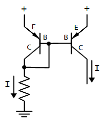
The following circuit shows how a current mirror is implemented.[7] A reference current passes through the transistor on the left. (In this case, the current is set by the resistor.) Since both transistors have the same emitter voltage and base voltage, they source the same current,[8] so the current on the right matches the reference current on the left.

Current mirror circuit. The current on the right copies the current on the left.

Current mirror circuit. The current on the right copies the current on the left.

A common use of a current mirror is to replace resistors. As explained earlier, resistors inside ICs are both inconveniently large and inaccurate. It saves space to use a current mirror instead of a resistor whenever possible. [9]

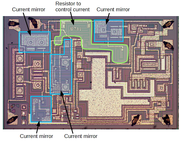
The diagram below shows that much of the 741 die is taken up by multiple current mirrors. The large resistor snaking around the upper middle of the IC controls the initial current. This current is then duplicated by multiple current mirrors, providing controlled currents to various parts of the chip. Using one large resistor and current mirrors is more compact and more accurate than using multiple large resistors. The current mirror in the middle is slightly different; it provides an active load for the input stage, improving the performance.

Die for the 741 op amp, showing the current mirrors, along with the resistor that controls the current.

Die for the 741 op amp, showing the current mirrors, along with the resistor that controls the current.

IC component: The differential pair

The second important circuit to understand is the differential pair, the most common two-transistor subcircuit used in analog ICs.[10] You may have wondered how the op amp subtracts two voltages; it's not obvious how to make a subtraction circuit. This is the job of the differential pair.

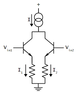
Schematic of a simple differential pair circuit. The current source sends a fixed current I through the differential pair. If the two inputs are equal, the current is split equally.

Schematic of a simple differential pair circuit. The current source sends a fixed current I through the differential pair. If the two inputs are equal, the current is split equally.

The schematic above shows a simple differential pair. The key is the current source at the top provides a fixed current I, which is split between the two input transistors. If the input voltages are equal, the current will be split equally into the two branches (I1 and I2). If one of the input voltages is a bit higher than the other, the corresponding transistor will conduct more current, so one branch gets more current and the other branch gets less. As one input continues to increase, more current gets pulled into that branch. Thus, the differential pair is a surprisingly simple circuit that routes current based on the difference in input voltages.

The internal blocks of the 741

The internal circuitry of the 741 op amp has been explained in many places[11], so I'll just give a brief description of the main blocks. The interactive chip viewer below provides more explanation.

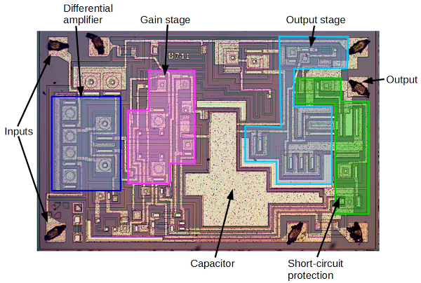
The two input pins are connected to the differential amplifier, which is based on the differential pair described above. The output from the differential amplifier goes to the second (gain) stage, which provides additional amplification of the signal. Finally, the output stage has large transistors to generate the high-current output, which is fed to the output pin.

Die for the 741 op amp, showing the main functional units.

Die for the 741 op amp, showing the main functional units.
A key innovation that led to the 741 was Fairchild's development of a new process for building capacitors on ICs using silicon nitride.[12] Op amps before the 741 required an external capacitor to prevent oscillation, which was inconvenient.[13] Dave Fullagar had the idea to put the compensation capacitor on the 741 chip using the new manufacturing process. Doing away with the external capacitor made the 741 extremely popular, either because engineers are lazy[14] or because the reduced part count was beneficial.

Another feature that made the 741 popular is its short-circuit protection. Many integrated circuits will overheat and self-destruct if you accidentally short circuit an output. The 741, though, includes clever circuits to shut down the output before damage occurs.

Interactive chip viewer

The die photo and schematic below are interactive. Click components in the die photo or schematic[15] to explore the chip, and a description will be displayed below. NPN transistors are highlighted in blue and PNP transistors are in red.

How I photographed the 741 die

Integrated circuit usually come in a black epoxy package. Dangerous concentrated acid is required to dissolve the epoxy package and see the die. But some ICs, such as the 741, are available in metal cans which can be easily opened with a hacksaw.[16] I used this safer approach. With even a basic middle-school microscope, you can get a good view of the die at low magnification but for the die photos, I used a metallurgical microscope, which shines light from above through the lens. A normal microscope shines light from below, which works well for transparent cells but not so well for opaque ICs. A metallurgical microscope is the secret to getting clear photos at higher magnification, since the die is brightly illuminated.[17]

Conclusion

Despite being almost 50 years old, the 741 op amp illustrates a lot of interesting features of analog integrated circuits. Next time you're listening to music, talking on your cell phone, or even just using your computer, think about the tiny op amps that make it possible and the 741 that's behind it all.

See more comments on Hacker News, Reddit and Hackaday. Los comentarios en español en Menéame.

We've got a winner! 741 op amp marketing letter from 1968. Courtesy of Dave Fullagar.

We've got a winner! 741 op amp marketing letter from 1968. Courtesy of Dave Fullagar.

Thanks to Dave Fullagar for providing information on the 741, including the letter above, which shows that the 741 was an instant success.

Notes and references

[1] The 741 op amp is one 25 Microchips That Shook the World and is popular enough to be on mugs and multiple tshirts, as well as available in a giant kit.

[2] To see the variety of circuits that can be built from an op amp, see this op amp circuit collection.

[3] You might have wondered why there is a distinction between the collector and emitter of a transistor, when the simple picture of a transistor is totally symmetrical. Both connect to an N layer, so why does it matter? As you can see from the die photo, the collector and emitter are very different in a real transistor. In addition to the very large size difference, the silicon doping is different. The result is a transistor will have poor gain if the collector and emitter are swapped.

[4] In many of the ICs that I've examined, it's easy to distinguish NPN and PNP transistors by their shape: NPN transistors are rectangular, while PNP transistors have circular emitters and bases with a circular metal layer on top. For some reason, this 741 chip uses rectangular and circular transistors for both NPN and PNP transistors. Thus, a closer examination is necessary to separate the NPN and PNP transistors.

[5] The capacitor in the 741 is located at a special point in the circuit where the effect of the capacitance is amplified due to something called the Miller effect. This allows the capacitor in the 741 to be much smaller than it would be otherwise. Given how much of the 741 die is used for the capacitor already, taking advantage of the Miller effect is very important.

[6] An alternative way to put capacitors on a chip is the junction capacitor, which is basically a large reverse-biased diode junction. The 741 doesn't use this technique; for more information on junction capacitors see my article on the TL431.

[7] For more information about current mirrors, you can check wikipedia, any analog IC book, or chapter 3 of Designing Analog Chips. If you're interested in how analog chips work, I strongly recommend you take a look at Designing Analog Chips.

[8] The current mirror doesn't provide exactly the same current for a variety of reasons. For instance, the base current is small but not zero. Transistor matching is very important: if the transistors are not identical, the currents will be different. (Using a single transistor with two collectors helps with matching.) If the collector voltages are different, the Early effect will cause the currents to be different. More complex current mirror circuits can reduce these problems.

[9] The 741 uses are several common extensions of the current source. First, by adding additional output transistors, you can create multiple copies of the current. Second, if you use a transistor with twice the collector size, you will get an output with twice the current (for instance). Third, instead of multiple output transistors, you can use one transistor with multiple collectors; this seems bizarre if you are used to discrete 3-pin transistors, but is a normal thing to do in IC designs. Finally, by flipping the circuit and using NPN transistors in place of PNP transistors, you can create a current sink, which is the same except current flows into the circuit instead of out of the circuit.

[10] Differential pairs are also called long-tailed pairs. According to Analysis and Design of Analog Integrated Circuits differential pairs are "perhaps the most widely used two-transistor subcircuits in monolithic analog circuits." (p214) For more information about differential pairs, see wikipedia, any analog IC book, or chapter 4 of Designing Analog Chips.

[11] You might expect 741 chips to all be pretty much the same, but the "741" name is really a category, not a single design. Manufacturers use diverse circuits for their 741 chips. Studying data sheet schematics, I found that 741 chips can be be divided into two categories based on the circuits for the second stage and output stage. The more common variant has 24 transistors, while the less common variant has 20 transistors. As far as I can tell, nobody has pointed this out before.

Wikipedia explains the 20-transistor variant while the 24-transistor variants are discussed in Operational Amplifiers IC Op-Amps Through the Ages, UNCC class notes and the book Microelectronic Circuits chapter 12. The 741 die I discuss in this article is the 24-transistor variant.

[12] For details on the 741's history, see this interesting discussion: Computer history museum: Fairchild Oral History Panel.

[13] If the output is too low, the feedback circuit pushes it higher. But if it goes too high, the feedback circuit pulls it lower. This could repeat, causing larger and larger oscillations. The capacitor blocks these oscillations. I've vastly oversimplified op amp stability and frequency compensation. Some more detailed discussions are here and here.

[14] IC Op-Amps Through the Ages says: "Despite a consequent near guarantee of suboptimal performance for most applications [because of the fixed capacitor], the ease of using the 741 has made it tremendously popular, proving Fullager's assumption that engineers are basically lazy (I mean, very time-efficient)."

[15] The schematic is from the Fairchild LM741 datasheet. I added the missing collector-base connection on Q12 and removed R12 (which is unused in this die). The component I photographed is the Analog Devices AD741, but that datasheet doesn't have a schematic.

[16] A plain hacksaw works to cut open an IC can. For later ICs, I used a jeweler's saw which gives a cleaner cut than a hacksaw - the IC doesn't look like it was ripped open by a bear. I got a saw on eBay for $14, and used the #2 blade. Make sure you cut near the top of the IC so you don't hit the internal pins or the die.

[17] To form the large image of the 741 die, I used Microsoft ICE to composite four images into a larger image. The Hugin photo stitcher can also be used for this, but I had trouble with it.