Macbook charger teardown: The surprising complexity inside Apple's power adapter

Have you ever wondered what's inside your Macbook's charger? There's a lot more circuitry crammed into the compact power adapter than you'd expect, including a microprocessor. This charger teardown looks at the numerous components in the charger and explains how they work together to power your laptop.

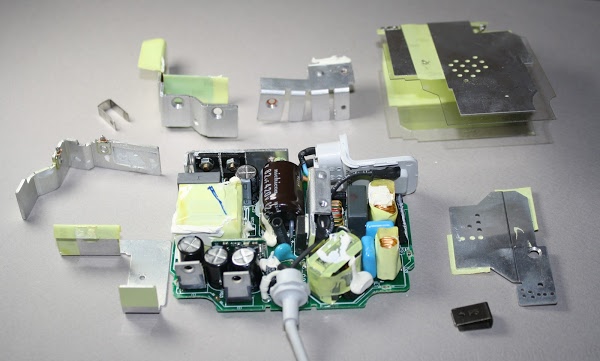
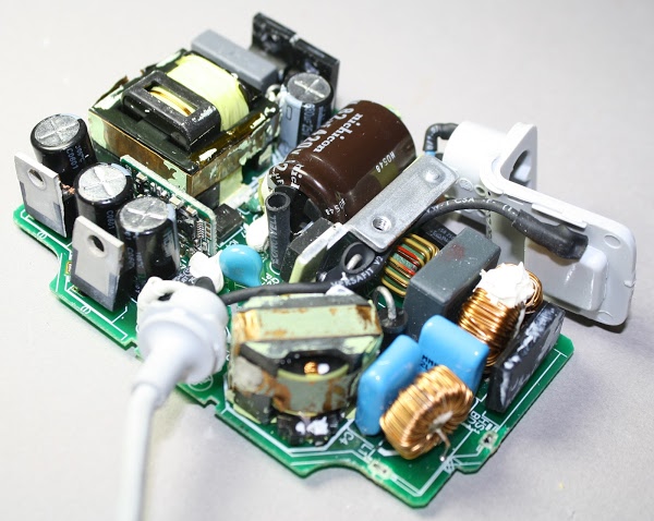
Inside the Macbook charger, after removing the heat sinks and insulating tape.

Inside the Macbook charger. Many electronic components work together to provide smooth power to your laptop.
Most consumer electronics, from your cell phone to your television, use a switching power supply to convert AC power from the wall to the low-voltage DC used by electronic circuits. The switching power supply gets its name because it switches power on and off thousands of times a second, which turns out to be a very efficient way to do this conversion.[1]

Switching power supplies are now very cheap, but this wasn't always the case. In the 1950s, switching power supplies were complex and expensive, used in aerospace and satellite applications that needed small, lightweight power supplies. By the early 1970s, new high-voltage transistors and other technology improvements made switching power supplies much cheaper and they became widely used in computers.[2] The introduction of a single-chip power supply controller in 1976 made switching power supplies simpler, smaller, and cheaper.

Apple's involvement with switching power supplies goes back to 1977 when Apple's chief engineer Rod Holt designed a switching power supply for the Apple II. According to Steve Jobs:[3]

"That switching power supply was as revolutionary as the Apple II logic board was. Rod doesn't get a lot of credit for this in the history books but he should. Every computer now uses switching power supplies, and they all rip off Rod Holt's design."

This is a fantastic quote, but unfortunately it is entirely false. The switching power supply revolution happened before Apple came along, Apple's design was similar to earlier power supplies[4] and other computers don't use Rod Holt's design. Nevertheless, Apple has extensively used switching power supplies and pushes the limits of charger design with their compact, stylish and advanced chargers.

Inside the charger

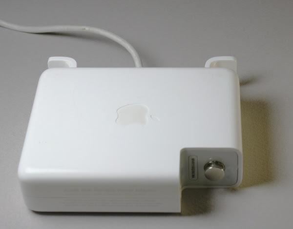
For the teardown I started with a Macbook 85W power supply, model A1172, which is small enough to hold in your palm. The picture below shows several features that can help distinguish the charger from counterfeits: the Apple logo in the case, the metal (not plastic) ground pin on the right, and the serial number next to the ground pin.

Apple 85W Macbook charger

Apple 85W Macbook charger
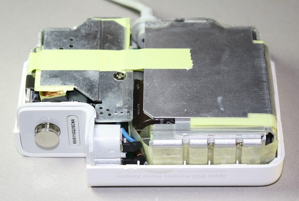
Strange as it seems, the best technique I've found for opening a charger is to pound on a wood chisel all around the seam to crack it open. With the case opened, the metal heat sinks of the charger are visible. The heat sinks help cool the high-power semiconductors inside the charger.

Inside the Apple 85W Macbook charger

Inside the Apple 85W Macbook charger
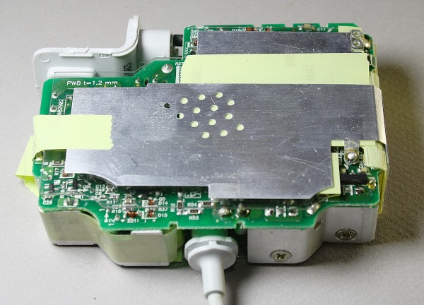
The other side of the charger shows the circuit board, with the power output at the bottom. Some of the tiny components are visible, but most of the circuitry is covered by the metal heat sink, held in place by yellow insulating tape.

The circuit board inside the Apple 85W Macbook charger.

The circuit board inside the Apple 85W Macbook charger. At the right, screws firmly attach components to the heat sinks.
After removing the metal heat sinks, the components of the charger are visible. These metal pieces give the charger a substantial heft, more than you'd expect from a small unit.

Exploded view of the Apple 85W charger

Exploded view of the Apple 85W charger, showing the extensive metal heat sinks.
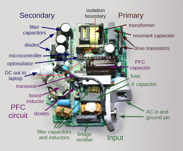
The diagram below labels the main components of the charger. AC power enters the charger and is converted to DC. The PFC circuit (Power Factor Correction) improves efficiency by ensuring the load on the AC line is steady. The primary chops up the high-voltage DC from the PFC circuit and feeds it into the transformer. Finally, the secondary receives low-voltage power from the transformer and outputs smooth DC to the laptop. The next few sections discuss these circuits in more detail, so follow along with the diagram below.

The components inside an Apple Macbook 85W power supply.

The components inside an Apple Macbook 85W power supply.

AC enters the charger

AC power enters the charger through a removable AC plug. A big advantage of switching power supplies is they can be designed to run on a wide range of input voltages. By simply swapping the plug, the charger can be used in any region of the world, from European 240 volts at 50 Hertz to North American 120 volts at 60 Hz. The filter capacitors and inductors in the input stage prevent interference from exiting the charger through the power lines. The bridge rectifier contains four diodes, which convert the AC power into DC. (See this video for a great demonstration of how a full bridge rectifier works.)

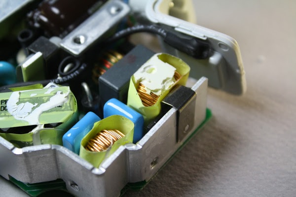
The input filtering in a Macbook charger. The diode bridge is attached to the metal heat sink with a clip.

The input components in a Macbook charger. The diode bridge rectifier is attached to the metal heat sink with a clip.

PFC: smoothing the power usage

The next step in the charger's operation is the Power Factor Correction circuit (PFC), labeled in purple. One problem with simple chargers is they only draw power during a small part of the AC cycle.[5] If too many devices do this, it causes problems for the power company. Regulations require larger chargers to use a technique called power factor correction so they use power more evenly.

The PFC circuit uses a power transistor to precisely chop up the input AC tens of thousands of times a second; contrary to what you might expect, this makes the load on the AC line smoother. Two of the largest components in the charger are the inductor and PFC capacitor that help boost the voltage to about 380 volts DC.[6]

The primary: chopping up the power

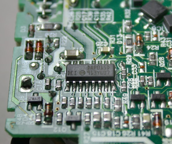
The primary circuit is the heart of the charger. It takes the high voltage DC from the PFC circuit, chops it up and feeds it into the transformer to generate the charger's low-voltage output (16.5-18.5 volts). The charger uses an advanced design called a resonant controller, which lets the system operate at a very high frequency, up to 500 kilohertz. The higher frequency permits smaller components to be used for a more compact charger. The chip below controls the switching power supply.[7]

The circuit board inside the Macbook charger. The chip in the middle controls the switching power supply circuit.

The circuit board inside the Macbook charger. The chip in the middle controls the switching power supply circuit.

The two drive transistors (in the overview diagram) alternately switch on and off to chop up the input voltage. The transformer and capacitor resonate at this frequency, smoothing the chopped-up input into a sine wave.

The secondary: smooth, clean power output

The secondary side of the circuit generates the output of the charger. The secondary receives power from the transformer and converts it DC with diodes. The filter capacitors smooth out the power, which leaves the charger through the output cable.

The most important role of the secondary is to keep the dangerous high voltages in the rest of the charger away from the output, to avoid potentially fatal shocks. The isolation boundary marked in red on the earlier diagram indicates the separation between the high-voltage primary and the low-voltage secondary. The two sides are separated by a distance of about 6 mm, and only special components can cross this boundary.

The transformer safely transmits power between the primary and the secondary by using magnetic fields instead of a direct electrical connection. The coils of wire inside the transformer are triple-insulated for safety. Cheap counterfeit chargers usually skimp on the insulation, posing a safety hazard. The optoisolator uses an internal beam of light to transmit a feedback signal between the secondary and primary. The control chip on the primary side uses this feedback signal to adjust the switching frequency to keep the output voltage stable.

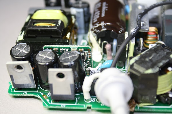
The output components in an Apple Macbook charger. The microcontroller board is visible behind the capacitors.

The output components in an Apple Macbook charger.The two power diodes are in front on the left. Behind them are three cylindrical filter capacitors.The microcontroller board is visible behind the capacitors.

A powerful microprocessor in your charger?

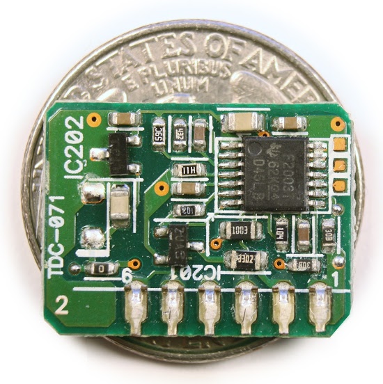
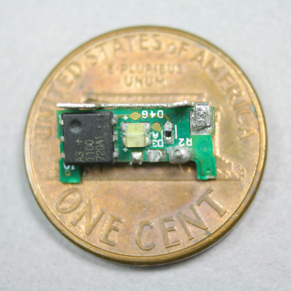
One unexpected component is a tiny circuit board with a microcontroller, which can be seen above. This 16-bit processor constantly monitors the charger's voltage and current. It enables the output when the charger is connected to a Macbook, disables the output when the charger is disconnected, and shuts the charger off if there is a problem. This processor is a Texas Instruments MSP430 microcontroller, roughly as powerful as the processor inside the original Macintosh.[8]

The microcontroller circuit board from an 85W Macbook power supply, on top of a quarter. The MPS430 processor monitors the charger's voltage and current.

The microcontroller circuit board from an 85W Macbook power supply, on top of a quarter. The MPS430 processor monitors the charger's voltage and current.

The square orange pads on the right are used to program software into the chip's flash memory during manufacturing.[9] The three-pin chip on the left (IC202) reduces the charger's 16.5 volts to the 3.3 volts required by the processor.[10]

The charger's underside: many tiny components

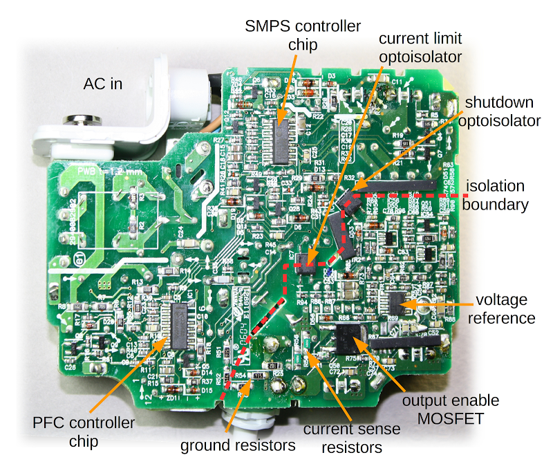
Turning the charger over reveals dozens of tiny components on the circuit board. The PFC controller chip and the power supply (SMPS) controller chip are the main integrated circuits controlling the charger. The voltage reference chip is responsible for keeping the voltage stable even as the temperature changes.[11] These chips are surrounded by tiny resistors, capacitors, diodes and other components. The output MOSFET transistor switches the power to the output on and off, as directed by the microcontroller. To the left of it, the current sense resistors measure the current flowing to the laptop.

The printed circuit board from an Apple 85W Macbook power supply, showing the tiny components inside the charger.

The printed circuit board from an Apple 85W Macbook power supply, showing the tiny components inside the charger.
The isolation boundary (marked in red) separates the high voltage circuitry from the low voltage output components for safety. The dashed red line shows the isolation boundary that separates the low-voltage side (bottom right) from the high-voltage side. The optoisolators send control signals from the secondary side to the primary, shutting down the charger if there is a malfunction.[12]

One reason the charger has more control components than a typical charger is its variable output voltage. To produce 60 watts, the charger provides 16.5 volts at 3.6 amps. For 85 watts, the voltage increases to 18.5 volts at 4.6 amps. This allows the charger to be compatible with lower-voltage 60 watt chargers, while still providing 85 watts for laptops that can use it.[13] As the current increases above 3.6 amps, the circuit gradually increases the output voltage. If the current increases too much, the charger abruptly shuts down around 90 watts.[14]

Inside the Magsafe connector

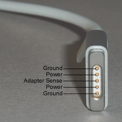
The magnetic Magsafe connector that plugs into the Macbook is more complex than you would expect. It has five spring-loaded pins (known as Pogo pins) to connect to the laptop. Two pins are power, two pins are ground, and the middle pin is a data connection to the laptop.

The pins of a Magsafe 2 connector. The pins are arranged symmetrically, so the connector can be plugged in either way.

The pins of a Magsafe 2 connector. The pins are arranged symmetrically, so the connector can be plugged in either way.
Inside the Magsafe connector is a tiny chip that informs the laptop of the charger's serial number, type, and power. The laptop uses this data to determine if the charger is valid. This chip also controls the status LEDs. There is no data connection to the charger block itself; the data connection is only with the chip inside the connector. For more details, see my article on the Magsafe connector.

The circuit board inside a Magsafe connector is very small. There are two LEDs on each side. The chip is a DS2413 1-Wire switch.

The circuit board inside a Magsafe connector is very small. There are two LEDs on each side. The chip is a DS2413 1-Wire switch.

Operation of the charger

You may have noticed that when you plug the connector into a Macbook, it takes a second or two for the LED to light up. During this time, there are complex interactions between the Macbook, the charger, and the Magsafe connector.

When the charger is disconnected from the laptop, the output transistor discussed earlier blocks the output power.[15] When the Magsafe connector is plugged into a Macbook, the laptop pulls the power line low.[16] The microcontroller in the charger detects this and after exactly one second enables the power output. The laptop then loads the charger information from the Magsafe connector chip. If all is well, the laptop starts pulling power from the charger and sends a command through the data pin to light the appropriate connector LED. When the Magsafe connector is unplugged from the laptop, the microcontroller detects the loss of current flow and shuts off the power, which also extinguishes the LEDs.

You might wonder why the Apple charger has all this complexity. Other laptop chargers simply provide 16 volts and when you plug it in, the computer uses the power. The main reason is for safety, to ensure that power isn't flowing until the connector is firmly attached to the laptop. This minimizes the risk of sparks or arcing while the Magsafe connector is being put into position.

Why you shouldn't get a cheap charger

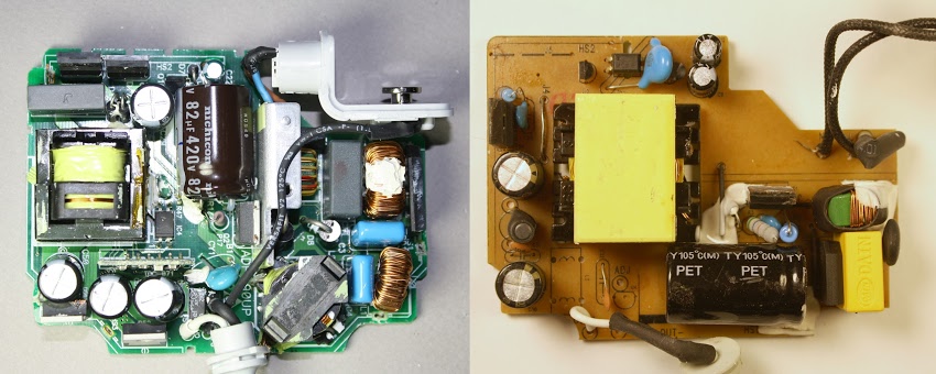
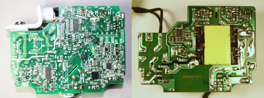
The Macbook 85W charger costs $79 from Apple, but for $14 you can get a charger on eBay that looks identical. Do you get anything for the extra $65? I opened up an imitation Macbook charger to see how it compares with the genuine charger. From the outside, the charger looks just like an 85W Apple charger except it lacks the Apple name and logo. But looking inside reveals big differences. The photos below show the genuine Apple charger on the left and the imitation on the right.

Inside the Apple 85W Macbook charger (left) vs an imitation charger (right). The genuine charger is crammed full of components, while the imitation has fewer parts.

Inside the Apple 85W Macbook charger (left) vs an imitation charger (right). The genuine charger is crammed full of components, while the imitation has fewer parts.

The imitation charger has about half the components of the genuine charger and a lot of blank space on the circuit board. While the genuine Apple charger is crammed full of components, the imitation leaves out a lot of filtering and regulation as well as the entire PFC circuit. The transformer in the imitation charger (big yellow rectangle) is much bulkier than in Apple's charger; the higher frequency of Apple's more advanced resonant converter allows a smaller transformer to be used.

The circuit board of the Apple 85W Macbook charger (left) compared with an imitation charger (right). The genuine charger has many more components.

The circuit board of the Apple 85W Macbook charger (left) compared with an imitation charger (right). The genuine charger has many more components.

Flipping the chargers over and looking at the circuit boards shows the much more complex circuitry of the Apple charger. The imitation charger has just one control IC (in the upper left).[17] since the PFC circuit is omitted entirely. In addition, the control circuits are much less complex and the imitation leaves out the ground connection.

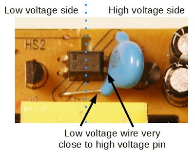
The imitation charger is actually better quality than I expected, compared to the awful counterfeit iPad charger and iPhone charger that I examined. The imitation Macbook charger didn't cut every corner possible and uses a moderately complex circuit. The imitation charger pays attention to safety, using insulating tape and keeping low and high voltages widely separated, except for one dangerous assembly error that can be seen below. The Y capacitor (blue) was installed crooked, so its connection lead from the low-voltage side ended up dangerously close to a pin on the high-voltage side of the optoisolator (black), creating a risk of shock.

Safety hazard inside an imitation Macbook charger. The lead of the Y capacitor is too close to the pin of the optoisolator, causing a risk of shock.

Safety hazard inside an imitation Macbook charger. The lead of the Y capacitor is too close to the pin of the optoisolator, causing a risk of shock.

Problems with Apple's chargers

The ironic thing about the Apple Macbook charger is that despite its complexity and attention to detail, it's not a reliable charger. When I told people I was doing a charger teardown, I rapidly collected a pile of broken chargers from people who had failed chargers. The charger cable is rather flimsy, leading to a class action lawsuit stating that the power adapter dangerously frays, sparks and prematurely fails to work. Apple provides detailed instructions on how to avoid damaging the wire, but a stronger cable would be a better solution. The result is reviews on the Apple website give the charger a dismal 1.5 out of 5 stars.

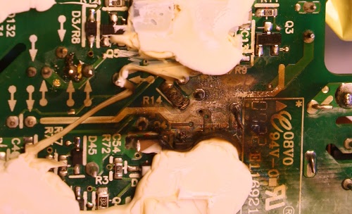
Burn mark inside an 85W Apple Macbook power supply that failed.

Burn mark inside an 85W Apple Macbook power supply that failed.

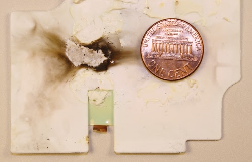
Macbook chargers also fail due to internal problems. The photos above and below show burn marks inside a failed Apple charger from my collection.[18] I can't tell exactly what went wrong, but something caused a short circuit that burnt up a few components. (The white gunk in the photo is insulating silicone used to mount the board.)

Burn marks inside an Apple Macbook charger that malfunctioned.

Burn marks inside an Apple Macbook charger that malfunctioned.

Why Apple's chargers are so expensive

As you can see, the genuine Apple charger has a much more advanced design than the imitation charger and includes more safety features. However, the genuine charger costs $65 more and I doubt the additional components cost more than $10 to $15[19]. Most of the cost of the charger goes into the healthy profit margin that Apple has on their products. Apple has an estimated 45% profit margin on iPhones[20] and chargers are probably even more profitable. Despite this, I don't recommend saving money with a cheap eBay charger due to the safety risk.

Conclusion

People don't give much thought to what's inside a charger, but a lot of interesting circuitry is crammed inside. The charger uses advanced techniques such as power factor correction and a resonant switching power supply to produce 85 watts of power in a compact, efficient unit. The Macbook charger is an impressive piece of engineering, even if it's not as reliable as you'd hope. On the other hand, cheap no-name chargers cut corners and often have safety issues, making them risky, both to you and your computer.

Notes and references

[1] The main alternative to a switching power supply is a linear power supply, which is much simpler and converts excess voltage to heat. Because of this wasted energy, linear power supplies are only about 60% efficient, compared to about 85% for a switching power supply. Linear power supplies also use a bulky transformer that may weigh multiple pounds, while switching power supplies can use a tiny high-frequency transformer.

[2] Switching power supplies were taking over the computer industry as early as 1971. Electronics World said that companies using switching regulators "read like a 'Who's Who' of the computer industry: IBM, Honeywell, Univac, DEC, Burroughs, and RCA, to name a few". See "The Switching Regulator Power Supply", Electronics World v86 October 1971, p43-47. In 1976, Silicon General introduced SG1524 PWM integrated circuit, which put the control circuitry for a switching power supply on a single chip.

[3] The quote about the Apple II power supply is from page 74 of the 2011 book Steve Jobs by Walter Isaacson. It inspired me to write a detailed history of switching power supplies: Apple didn't revolutionize power supplies; new transistors did. Steve Job's quote sounds convincing, but I consider it the reality distortion field in effect.

[4] If anyone can take the credit for making switching power supplies an inexpensive everyday product, it is Robert Boschert. He started selling switching power supplies in 1974 for everything from printers and computers to the F-14 fighter plane. See Robert Boschert: A Man Of Many Hats Changes The World Of Power Supplies in Electronic Design. The Apple II's power supply is very similar to the Boschert OL25 flyback power supply but with a patented variation.

[5] You might expect the bad power factor is because switching power supplies rapidly turn on and off, but that's not the problem. The difficulty comes from the nonlinear diode bridge, which charges the input capacitor only at peaks of the AC signal. (If you're familiar with power factors due to phase shift, this is totally different. The problem is the non-sinusoidal current, not a phase shift.)

The idea behind PFC is to use a DC-DC boost converter before the switching power supply itself. The boost converter is carefully controlled so its input current is a sinusoid proportional to the AC waveform. The result is the boost converter looks like a nice resistive load to the power line, and the boost converter supplies steady voltage to the switching power supply components.

[6] The charger uses a MC33368 "High Voltage GreenLine Power Factor Controller" chip to run the PFC. The chip is designed for low power, high-density applications so it's a good match for the charger.

[7] The SMPS controller chip is a L6599 high-voltage resonant controller; for some reason it is labeled DAP015D. It uses a resonant half-bridge topology; in a half-bridge circuit, two transistors control power through the transformer first one direction and then the other. Common switching power supplies use a PWM (pulse width modulation) controller, which adjusts the time the input is on. The L6599, on the other hand, adjusts the frequency instead of the pulse width. The two transistors alternate switching on for 50% of the time. As the frequency increases above the resonant frequency, the power drops, so controlling the frequency regulates the output voltage.

[8] The processor in the charger is a MSP430F2003 ultra low power microcontroller with 1kB of flash and just 128 bytes of RAM. It includes a high-precision 16-bit analog to digital converter. More information is here.

The 68000 microprocessor from the original Apple Macintosh and the 430 microcontroller in the charger aren't directly comparable as they have very different designs and instruction sets. But for a rough comparison, the 68000 is a 16/32 bit processor running at 7.8MHz, while the MSP430 is a 16 bit processor running at 16MHz. The Dhrystone benchmark measures 1.4 MIPS (million instructions per second) for the 68000 and much higher performance of 4.6 MIPS for the MSP430. The MSP430 is designed for low power consumption, using about 1% of the power of the 68000.

[9] The 60W Macbook charger uses a custom MSP430 processor, but the 85W charger uses a general-purpose processor that needs to loaded with firmware. The chip is programmed with the Spy-Bi-Wire interface, which is TI's two-wire variant of the standard JTAG interface. After programming, a security fuse inside the chip is blown to prevent anyone from reading or modifying the firmware.

[10] The voltage to the processor is provided by not by a standard voltage regulator, but a LT1460 precision reference, which outputs 3.3 volts with the exceptionally high accuracy of 0.075%. This seems like overkill to me; this chip is the second-most expensive chip in the charger after the SMPS controller, based on Octopart's prices.

[11] The voltage reference chip is unusual, it is a TSM103/A that combines two op amps and a 2.5V reference in a single chip. Semiconductor properties vary widely with temperature, so keeping the voltage stable isn't straightforward. A clever circuit called a bandgap reference cancels out temperature variations; I explain it in detail here.

[12] Since some readers are very interested in grounding, I'll give more details. A 1KΩ ground resistor connects the AC ground pin to the charger's output ground. (With the 2-pin plug, the AC ground pin is not connected.) Four 9.1MΩ resistors connect the internal DC ground to the output ground. Since they cross the isolation boundary, safety is an issue. Their high resistance avoids a shock hazard. In addition, since there are four resistors in series for redundancy, the charger remains safe even if a resistor shorts out somehow. There is also a Y capacitor (680pF, 250V) between the internal ground and output ground; this blue capacitor is on the upper side of the board. A T5A fuse (5 amps) protects the output ground.

[13] The power in watts is simply the volts multiplied by the amps. Increasing the voltage is beneficial because it allows higher wattage; the maximum current is limited by the wire size.

[14] The control circuitry is fairly complex. The output voltage is monitored by an op amp in the TSM103/A chip which compares it with a reference voltage generated by the same chip. This amplifier sends a feedback signal via an optoisolator to the SMPS control chip on the primary side. If the voltage is too high, the feedback signal lowers the voltage and vice versa. That part is normal for a power supply, but ramping the voltage from 16.5 volts to 18.5 volts is where things get complicated.

The output current creates a voltage across the current sense resistors, which have a tiny resistance of 0.005Ω each - they are more like wires than resistors. An op amp in the TSM103/A chip amplifies this voltage. This signal goes to tiny TS321 op amp which starts ramping up when the signal corresponds to 4.1A. This signal goes into the previously-described monitoring circuit, increasing the output voltage.

The current signal also goes into a tiny TS391 comparator, which sends a signal to the primary through another optoisolator to cut the output voltage. This appears to be a protection circuit if the current gets too high. The circuit board has a few spots where zero-ohm resistors (i.e. jumpers) can be installed to change the op amp's amplification. This allows the amplification to be adjusted for accuracy during manufacture.

[15] If you measure the voltage from a Macbook charger, you'll find about six volts instead of the 16.5 volts you'd expect. The reason is the output is deactivated and you're only measuring the voltage through the bypass resistor just below the output transistor.

[16] The laptop pulls the charger output low with a 39.41KΩ resistor to indicate that it is ready for power. An interesting thing is it won't work to pull the output too low - shorting the output to ground doesn't work. This provides a safety feature. Accidental contact with the pins is unlikely to pull the output to the right level, so the charger is unlikely to energize except when properly connected.

[17] The imitation charger uses the Fairchild FAN7602 Green PWM Controller chip, which is more advanced than I expected in a knock-off; I wouldn't have been surprised if it just used a simple transistor oscillator. Another thing to note is the imitation charger uses a single-sided circuit board, while the genuine uses a double-sided circuit board, due to the much more complex circuit.

[18] The burnt charger is an Apple A1222 85W Macbook charger, which is a different model from the A1172 charger in the rest of the teardown. The A1222 is in a slightly smaller, square case and has a totally different design based on the NCP 1203 PWM controller chip. Components in the A1222 charger are packed even more tightly than in the A1172 charger. Based on the burnt-up charger, I think they pushed the density a bit too far.

[19] I looked up many of the charger components on Octopart to see their prices. Apple's prices should be considerably lower. The charger has many tiny resistors, capacitors and transistors; they cost less than a cent each. The larger power semiconductors, capacitors and inductors cost considerably more. I was surprised that the 16-bit MSP430 processor costs only about $0.45. I estimated the price of the custom transformers. The list below shows the main components.

ComponentCost
MSP430F2003 processor$0.45
MC33368D PFC chip$0.50
L6599 controller chip$1.62
LT1460 3.3V reference$1.46
TSM103/A reference$0.16
2x P11NM60AFP 11A 600V MOSFET$2.00
3x Vishay optocoupler$0.48
2x 630V 0.47uF film capacitor$0.88
4x 25V 680uF electrolytic capacitor$0.12
420V 82uF electrolytic capacitor$0.93
polypropylene X2 capacitor$0.17
3x toroidal inductor$0.75
4A 600V diode bridge$0.40
2x dual common-cathode schottky rectifier 60V, 15A$0.80
20NC603 power MOSFET$1.57
transformer$1.50?
PFC inductor$1.50?

[20] The article Breaking down the full $650 cost of the iPhone 5 describes Apple's profit margins in detail, estimating 45% profit margin on the iPhone. Some people have suggested that Apple's research and development expenses explain the high cost of their chargers, but the math shows R&D costs must be negligible. The book Practical Switching Power Supply Design estimates 9 worker-months to design and perfect a switching power supply, so perhaps $200,000 of engineering cost. More than 20 million Macbooks are sold per year, so the R&D cost per charger would be one cent. Even assuming the Macbook charger requires ten times the development of a standard power supply only increases the cost to 10 cents.
Understanding silicon circuits: inside the ubiquitous 741 op amp

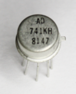
The 741 op amp is one of the most famous and popular ICs[1] with hundreds of millions sold since its invention in 1968 by famous IC designer Dave Fullagar. In this article, I look at the silicon die for the 741, discuss how it works, and explain how circuits are built from silicon.

The 741 op amp, packaged in a TO-99 metal can.

The 741 op amp, packaged in a TO-99 metal can.

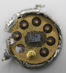
I started with a 741 op amp that was packaged in a metal can (above). Cutting the top off with a hacksaw reveals the tiny silicon die (below), connected to the pins by fine wires.

Inside a 741 op amp, showing the die. This is a TO-99 metal can package, with the top sawed off

Inside a 741 op amp, showing the die. This is a TO-99 metal can package, with the top sawed off

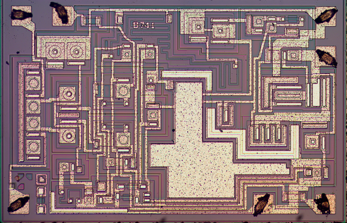
Under a microscope, the details of the silicon chip are visible, as shown below. At first, the chip looks like an incomprehensible maze, but this article will show how transistors, resistors and capacitors are formed on the chip, and explain how they combine to make the op amp.

Die photo of the 741 op amp

Die photo of the 741 op amp

Why op amps are important

Op amps are a key component in analog circuits. An op amp takes two input voltages, subtracts them, multiplies the difference by a huge value (100,000 or more), and outputs the result as a voltage. If you've studied analog circuits, op amps will be familiar to you, but otherwise this may seem like a bizarre and pointless device. How often do you need to subtract two voltages? And why amplify by such a huge factor: will a 1 volt input result in lightning shooting from the op amp? The answer is feedback: by using a feedback signal, the output becomes a sensible value and the high amplification makes the circuit performance stable.

Op amps are used as amplifiers, filters, integrators, differentiators, and many other circuits.[2] Op amps are all around you: your computer's power supply uses op amps for regulation. Your cell phone uses op amps for filtering and amplifying audio signals, camera signals, and the broadcast cell signal.

The structure of the integrated circuit

NPN transistors inside the IC

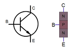
Transistors are the key components in a chip. If you've studied electronics, you've probably seen a diagram of a NPN transistor like the one below, showing the collector (C), base (B), and emitter (E) of the transistor, The transistor is illustrated as a sandwich of P silicon in between two symmetric layers of N silicon; the N-P-N layers make a NPN transistor. It turns out that transistors on a chip look nothing like this, and the base often isn't even in the middle!

Symbol and oversimplified structure of an NPN transistor.

Symbol and oversimplified structure of an NPN transistor.

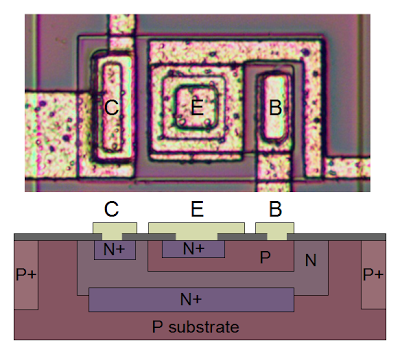
The photo below shows one of the transistors in the 741 as it appears on the chip. The different brown and purple colors are regions of silicon that has been doped differently, forming N and P regions. The whitish-yellow areas are the metal layer of the chip on top of the silicon - these form the wires connecting to the collector, emitter, and base.

Underneath the photo is a cross-section drawing showing approximately how the transistor is constructed. There's a lot more than just the N-P-N sandwich you see in books, but if you look carefully at the vertical cross section below the 'E', you can find the N-P-N that forms the transistor. The emitter (E) wire is connected to N+ silicon. Below that is a P layer connected to the base contact (B). And below that is a N+ layer connected (indirectly) to the collector (C).[3] The transistor is surrounded by a P+ ring that isolates it from neighboring components.
Structure of a NPN transistor in the 741 op amp

Structure of a NPN transistor in the 741 op amp

PNP transistors inside the IC

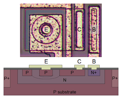
You might expect PNP transistors to be similar to NPN transistors, just swapping the roles of N and P silicon. But for a variety of reasons, PNP transistors have an entirely different construction. They consist of a circular emitter (P), surrounded by a ring shaped base (N), which is surrounded by the collector (P).[4] This forms a P-N-P sandwich horizontally (laterally), unlike the vertical structure of the NPN transistors.

The diagram below shows one of the PNP transistors in the 741, along with a cross-section showing the silicon structure. Note that although the metal contact for the base is on the edge of the transistor, it is electrically connected through the N and N+ regions to its active ring in between the collector and emitter.

Structure of a PNP transistor in the 741 op amp.

Structure of a PNP transistor in the 741 op amp.

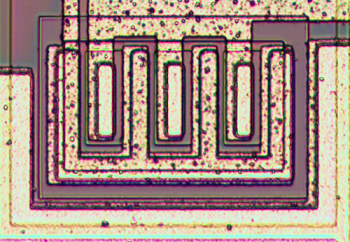
The output transistors in the 741 are larger than the other transistors and have a different structure in order to produce the high-current output. The output transistors must support 25mA, compared to microamps for the internal transistors. The photo below shows one of the output transistors. Note the multiple interlocking "fingers" of the emitter and base, surrounded by the large collector.

A high-current PNP transistor inside the 741 op amp

A high-current PNP transistor inside the 741 op amp

How resistors are implemented in silicon

Resistors are a key component of analog chips. Unfortunately, resistors in ICs are very inaccurate; the resistances can vary by 50% from chip to chip. Thus, analog ICs are designed so only the ratio of resistors matters, not the absolute values, since the ratios remain nearly constant from chip to chip.

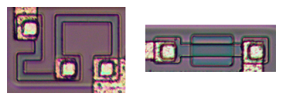
The photo below shows two resistors in the 741 op amp, formed using different techniques. The resistor on the left is formed from a meandering strip of P silicon, and is about 5KΩ. The resistor on the right is a pinch resistor and is about 50KΩ. In the pinch resistor, a layer of N silicon on top makes the conductive region much thinner (i.e. pinches it). This allows a much higher resistance for a given size. Both resistors are at the same scale below, but the pinch resistor has ten times the resistance. The tradeoff is the pinch resistor is much less accurate.

Two resistors from the 741 op amp. The left resistor is a simple 'base resistor', while the right resistor is a 'pinch resistor'.

Two resistors from the 741 op amp. The left resistor is a simple 'base resistor', while the right resistor is a 'pinch resistor'.

How capacitors are implemented in silicon

The 741's capacitor is essentially a large metal plate separated from the silicon by an insulating layer. The main drawback of capacitors on ICs is they are physically very large. The 25pF capacitor in the 741 has a very small value but takes up a large fraction of the chip's area.[5][6] You can see the capacitor in the middle of the die photo; it is the largest structure on the chip.

IC component: The current mirror

There are some subcircuits that are very common in analog ICs, but may seem mysterious at first. Before explaining the 741's circuit, I'll first give a brief overview of the current mirror and differential pair circuits.

Schematic symbols for a current source.

Schematic symbols for a current source.

If you've looked at analog IC block diagrams, you may have seen the above symbols for a current source and wondered what a current source is and why you'd use one. The idea of a current source is you start with one known current and then you can "clone" multiple copies of the current with a simple transistor circuit.

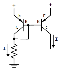
The following circuit shows how a current mirror is implemented.[7] A reference current passes through the transistor on the left. (In this case, the current is set by the resistor.) Since both transistors have the same emitter voltage and base voltage, they source the same current,[8] so the current on the right matches the reference current on the left.

Current mirror circuit. The current on the right copies the current on the left.

Current mirror circuit. The current on the right copies the current on the left.

A common use of a current mirror is to replace resistors. As explained earlier, resistors inside ICs are both inconveniently large and inaccurate. It saves space to use a current mirror instead of a resistor whenever possible. [9]

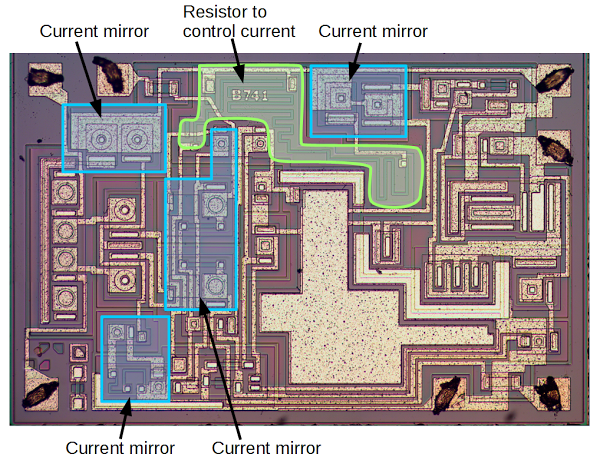
The diagram below shows that much of the 741 die is taken up by multiple current mirrors. The large resistor snaking around the upper middle of the IC controls the initial current. This current is then duplicated by multiple current mirrors, providing controlled currents to various parts of the chip. Using one large resistor and current mirrors is more compact and more accurate than using multiple large resistors. The current mirror in the middle is slightly different; it provides an active load for the input stage, improving the performance.

Die for the 741 op amp, showing the current mirrors, along with the resistor that controls the current.

Die for the 741 op amp, showing the current mirrors, along with the resistor that controls the current.

IC component: The differential pair

The second important circuit to understand is the differential pair, the most common two-transistor subcircuit used in analog ICs.[10] You may have wondered how the op amp subtracts two voltages; it's not obvious how to make a subtraction circuit. This is the job of the differential pair.

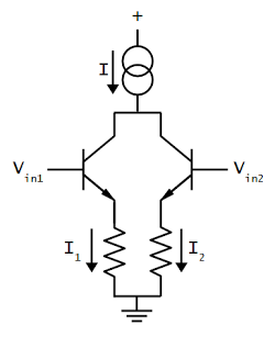
Schematic of a simple differential pair circuit. The current source sends a fixed current I through the differential pair. If the two inputs are equal, the current is split equally.

Schematic of a simple differential pair circuit. The current source sends a fixed current I through the differential pair. If the two inputs are equal, the current is split equally.

The schematic above shows a simple differential pair. The key is the current source at the top provides a fixed current I, which is split between the two input transistors. If the input voltages are equal, the current will be split equally into the two branches (I1 and I2). If one of the input voltages is a bit higher than the other, the corresponding transistor will conduct more current, so one branch gets more current and the other branch gets less. As one input continues to increase, more current gets pulled into that branch. Thus, the differential pair is a surprisingly simple circuit that routes current based on the difference in input voltages.

The internal blocks of the 741

The internal circuitry of the 741 op amp has been explained in many places[11], so I'll just give a brief description of the main blocks. The interactive chip viewer below provides more explanation.

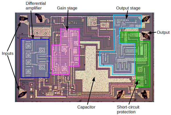
The two input pins are connected to the differential amplifier, which is based on the differential pair described above. The output from the differential amplifier goes to the second (gain) stage, which provides additional amplification of the signal. Finally, the output stage has large transistors to generate the high-current output, which is fed to the output pin.

Die for the 741 op amp, showing the main functional units.

Die for the 741 op amp, showing the main functional units.
A key innovation that led to the 741 was Fairchild's development of a new process for building capacitors on ICs using silicon nitride.[12] Op amps before the 741 required an external capacitor to prevent oscillation, which was inconvenient.[13] Dave Fullagar had the idea to put the compensation capacitor on the 741 chip using the new manufacturing process. Doing away with the external capacitor made the 741 extremely popular, either because engineers are lazy[14] or because the reduced part count was beneficial.

Another feature that made the 741 popular is its short-circuit protection. Many integrated circuits will overheat and self-destruct if you accidentally short circuit an output. The 741, though, includes clever circuits to shut down the output before damage occurs.

Interactive chip viewer

The die photo and schematic below are interactive. Click components in the die photo or schematic[15] to explore the chip, and a description will be displayed below. NPN transistors are highlighted in blue and PNP transistors are in red.

How I photographed the 741 die

Integrated circuit usually come in a black epoxy package. Dangerous concentrated acid is required to dissolve the epoxy package and see the die. But some ICs, such as the 741, are available in metal cans which can be easily opened with a hacksaw.[16] I used this safer approach. With even a basic middle-school microscope, you can get a good view of the die at low magnification but for the die photos, I used a metallurgical microscope, which shines light from above through the lens. A normal microscope shines light from below, which works well for transparent cells but not so well for opaque ICs. A metallurgical microscope is the secret to getting clear photos at higher magnification, since the die is brightly illuminated.[17]

Conclusion

Despite being almost 50 years old, the 741 op amp illustrates a lot of interesting features of analog integrated circuits. Next time you're listening to music, talking on your cell phone, or even just using your computer, think about the tiny op amps that make it possible and the 741 that's behind it all.

See more comments on Hacker News, Reddit and Hackaday. Los comentarios en español en Menéame.

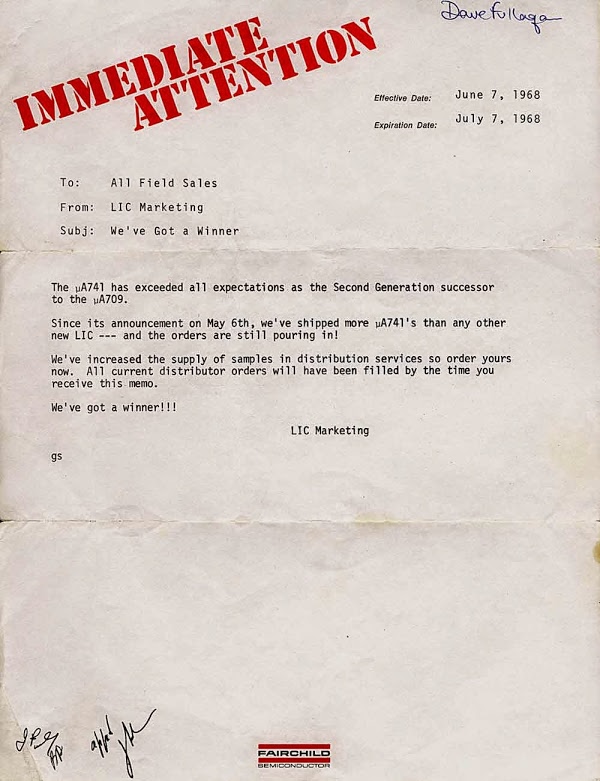
We've got a winner! 741 op amp marketing letter from 1968. Courtesy of Dave Fullagar.

We've got a winner! 741 op amp marketing letter from 1968. Courtesy of Dave Fullagar.

Thanks to Dave Fullagar for providing information on the 741, including the letter above, which shows that the 741 was an instant success.

Notes and references

[1] The 741 op amp is one 25 Microchips That Shook the World and is popular enough to be on mugs and multiple tshirts, as well as available in a giant kit.

[2] To see the variety of circuits that can be built from an op amp, see this op amp circuit collection.

[3] You might have wondered why there is a distinction between the collector and emitter of a transistor, when the simple picture of a transistor is totally symmetrical. Both connect to an N layer, so why does it matter? As you can see from the die photo, the collector and emitter are very different in a real transistor. In addition to the very large size difference, the silicon doping is different. The result is a transistor will have poor gain if the collector and emitter are swapped.

[4] In many of the ICs that I've examined, it's easy to distinguish NPN and PNP transistors by their shape: NPN transistors are rectangular, while PNP transistors have circular emitters and bases with a circular metal layer on top. For some reason, this 741 chip uses rectangular and circular transistors for both NPN and PNP transistors. Thus, a closer examination is necessary to separate the NPN and PNP transistors.

[5] The capacitor in the 741 is located at a special point in the circuit where the effect of the capacitance is amplified due to something called the Miller effect. This allows the capacitor in the 741 to be much smaller than it would be otherwise. Given how much of the 741 die is used for the capacitor already, taking advantage of the Miller effect is very important.

[6] An alternative way to put capacitors on a chip is the junction capacitor, which is basically a large reverse-biased diode junction. The 741 doesn't use this technique; for more information on junction capacitors see my article on the TL431.

[7] For more information about current mirrors, you can check wikipedia, any analog IC book, or chapter 3 of Designing Analog Chips. If you're interested in how analog chips work, I strongly recommend you take a look at Designing Analog Chips.

[8] The current mirror doesn't provide exactly the same current for a variety of reasons. For instance, the base current is small but not zero. Transistor matching is very important: if the transistors are not identical, the currents will be different. (Using a single transistor with two collectors helps with matching.) If the collector voltages are different, the Early effect will cause the currents to be different. More complex current mirror circuits can reduce these problems.

[9] The 741 uses are several common extensions of the current source. First, by adding additional output transistors, you can create multiple copies of the current. Second, if you use a transistor with twice the collector size, you will get an output with twice the current (for instance). Third, instead of multiple output transistors, you can use one transistor with multiple collectors; this seems bizarre if you are used to discrete 3-pin transistors, but is a normal thing to do in IC designs. Finally, by flipping the circuit and using NPN transistors in place of PNP transistors, you can create a current sink, which is the same except current flows into the circuit instead of out of the circuit.

[10] Differential pairs are also called long-tailed pairs. According to Analysis and Design of Analog Integrated Circuits differential pairs are "perhaps the most widely used two-transistor subcircuits in monolithic analog circuits." (p214) For more information about differential pairs, see wikipedia, any analog IC book, or chapter 4 of Designing Analog Chips.

[11] You might expect 741 chips to all be pretty much the same, but the "741" name is really a category, not a single design. Manufacturers use diverse circuits for their 741 chips. Studying data sheet schematics, I found that 741 chips can be be divided into two categories based on the circuits for the second stage and output stage. The more common variant has 24 transistors, while the less common variant has 20 transistors. As far as I can tell, nobody has pointed this out before.

Wikipedia explains the 20-transistor variant while the 24-transistor variants are discussed in Operational Amplifiers IC Op-Amps Through the Ages, UNCC class notes and the book Microelectronic Circuits chapter 12. The 741 die I discuss in this article is the 24-transistor variant.

[12] For details on the 741's history, see this interesting discussion: Computer history museum: Fairchild Oral History Panel.

[13] If the output is too low, the feedback circuit pushes it higher. But if it goes too high, the feedback circuit pulls it lower. This could repeat, causing larger and larger oscillations. The capacitor blocks these oscillations. I've vastly oversimplified op amp stability and frequency compensation. Some more detailed discussions are here and here.

[14] IC Op-Amps Through the Ages says: "Despite a consequent near guarantee of suboptimal performance for most applications [because of the fixed capacitor], the ease of using the 741 has made it tremendously popular, proving Fullager's assumption that engineers are basically lazy (I mean, very time-efficient)."

[15] The schematic is from the Fairchild LM741 datasheet. I added the missing collector-base connection on Q12 and removed R12 (which is unused in this die). The component I photographed is the Analog Devices AD741, but that datasheet doesn't have a schematic.

[16] A plain hacksaw works to cut open an IC can. For later ICs, I used a jeweler's saw which gives a cleaner cut than a hacksaw - the IC doesn't look like it was ripped open by a bear. I got a saw on eBay for $14, and used the #2 blade. Make sure you cut near the top of the IC so you don't hit the internal pins or the die.

[17] To form the large image of the 741 die, I used Microsoft ICE to composite four images into a larger image. The Hugin photo stitcher can also be used for this, but I had trouble with it.

Qui-binary arithmetic: how a 1960s IBM mainframe does math

The IBM 1401 computer uses an unusual technique called qui-binary arithmetic to perform arithmetic. In the early 1960s, the IBM 1401 was the most popular computer, used by many businesses for the low monthly price of $2500. For a business computer, error detection was critical: if a company sent out bad payroll checks because of a hardware fault, it would be catastrophic. By using qui-binary arithmetic, the IBM 1401 detects arithmetic errors.

If you've studied digital circuits, you've seen the standard binary adder circuits that add two numbers. But the IBM 1401 uses a totally different approach. Unlike modern computers, the IBM 1401 operates on decimal digits, not binary numbers, using BCD (binary-coded decimal). To add two numbers, digits are converted from BCD to qui-binary, added together with a special qui-binary adder, and then converted back to digits in BCD. This may seem pointlessly complex, but it allows easy error detection.

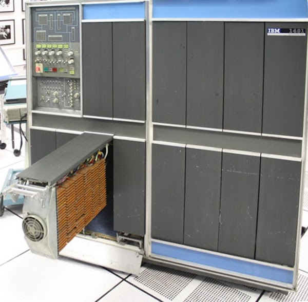
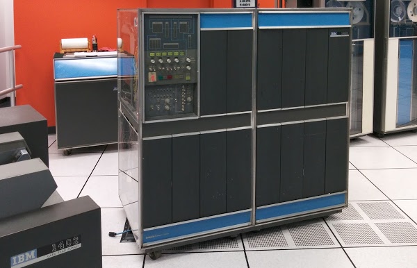
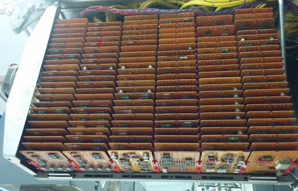
The photo below shows the IBM 1401 with one panel opened to show the addition/subtraction circuitry, made up of dozens of Standard Module System (SMS) cards. Each SMS card holds a simple circuit with a few germanium transistors (the computer predates silicon transistors). This article explains in detail how these circuits implement it.

The IBM 1401 mainframe with gate 01B3 opened. This gate contains the arithmetic circuitry, made up of many SMS cards.

The IBM 1401 mainframe with gate 01B3 opened. This gate contains the arithmetic circuitry, made up of many SMS cards.

What is qui-binary?

Qui-binary code is a way of representing a decimal digit with 7 bits. The number is split into a qui part (0, 2, 4, 6, or 8) and a binary part (0 or 1).[1] For example, 3 is split into 2+1, and 8 is split into 8+0. The qui part is labeled Q0, Q2, Q4, Q6, or Q8 and the binary part is B0 or B1. The number is then represented by seven bits: Q8Q6Q4Q2Q0B1B0. The following table summarizes the qui-binary representation.

DigitQuiBinary Bits: Q8Q6Q4Q2Q0B1B0
0Q0B00000101
1Q0B10000110
2Q2B00001001
3Q2B10001010
4Q4B00010001
5Q4B10010010
6Q6B00100001
7Q6B10100010
8Q8B01000001
9Q8B11000010

The advantage of qui-binary is error detection, since it is straightforward to detect an invalid qui-binary number.[2] A valid qui-binary number has exactly one qui bit and exactly one binary bit. Any other qui-binary number is faulty. For instance, Q4 Q2 B0 is bad, as is Q8. A problem in any bit creates a bad qui-binary number and can be detected.

Overview of the 1401's qui-binary circuit

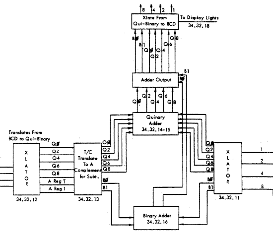
The IBM 1401's arithmetic unit operates on one digit at a time, adding them with a qui-binary adder.[3] The block diagram below[4] shows how the adder takes two binary-coded decimal digits, stored in the A and B temporary registers, and produces their sum. The digit from the A register enters on the left, and is translated to qui-binary by the translation circuit (labeled XLATOR). This qui-binary value goes through a translate/complement circuit which is used for subtraction. The digit in the B register enters on the right and is also converted to qui-binary. The binary bits (B0/B1) are added by the binary adder at the bottom. The quinary values are added with a special quinary adder. The adder output circuit combines the quinary bits with any carry, generating the qui-binary result. Finally, the translation circuit at the top converts the qui-binary result back to a BCD digit, sending the BCD value to core memory and to the console display lights.[5]

Overview of the arithmetic unit in the IBM 1401 mainframe.

Overview of the arithmetic unit in the IBM 1401 mainframe.

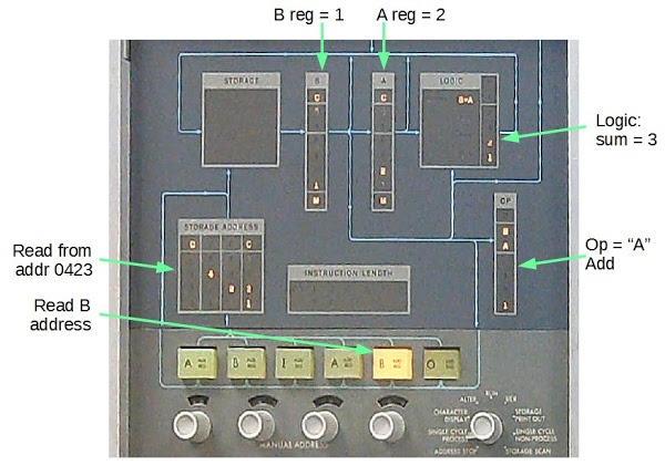
The photo below shows the IBM 1401 console during an addition instruction. The numbers are displayed in binary-coded decimal; the qui-binary representation is entirely hidden from the programmer. At this point in the addition instruction, the digit 1 was read from address 423 into the B register, and is added to the digit 2 already in the A register. The result from the qui-binary adder is 3 (binary 2 + 1), which is stored back to memory.[6]

The IBM 1401 console, showing an addition operation.

The IBM 1401 console, showing an addition operation.

BCD to qui-binary translation

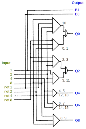
To examine the addition/subtraction circuitry in more detail, we'll start with the logic that converts a BCD digit to qui-binary. The logic is implement with an AND-OR structure that is common in the 1401. Note that the logic gate symbols are different from modern symbols: an AND gate is represented as a triangle, and an OR gate is represented as a semi-circle. Each bit of the BCD digit, as well as the bit's complement, is provided as input. Each AND gate matches a specific bit pattern, and then the results are combined with an OR gate to generate an output.

The circuit in an IBM 1401 mainframe to translate a BCD digit into qui-binary code.

The circuit in an IBM 1401 mainframe to translate a BCD digit into qui-binary code.

To see how this works, look at the AND gate at the bottom (labeled 8, 9). Tracing the wires to the inputs, this gate will be active if input 8 AND input not-4 AND input not-2 are set, i.e. if the input is binary 1000 or 1001. Thus, output Q8 will be set if the input digit is 8 or 9, just as required for the qui-binary code.

For a slightly more complicated case, the first AND gate matches binary 1010 (decimal 10), and the second AND gate matches binary 000x (decimal 0 or 1). Thus, Q0 will be set for inputs 0, 1, or 10. Likewise, Q2 is set for inputs 2, 3, or 11. The other Q outputs are simpler, computed with a single AND gate.[7]

The B0 and B1 outputs are simply wires from the not-1 and 1 inputs. If the input is even, B0 is set, and if the input is odd, B1 is set.

9's complement circuit

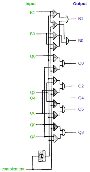
To perform subtraction, the IBM 1401 adds the 9's complement of the digit. The 9's complement is simply 9 minus the digit. The complement circuit below passes the qui-binary number through unchanged for addition or complemented for subtraction.[8] The complement input selects which mode to use; it is generated from the operation (addition or subtraction), and the signs of the input numbers.

To see how complementation works in qui-binary, consider 3 (Q2 B1). Its complement is 6 (Q6 B0). The general pattern for complementation is B0 and B1 get swapped. Q0 and Q8 are swapped, and Q2 and Q6 are swapped. Q4 is unchanged; for example, 4 (Q4 B0) is complemented to 5 (Q4 B1).[9]

The complement circuit from the IBM 1401 mainframe. This converts a digit to its 9's complement value.

The complement circuit from the IBM 1401 mainframe. This converts a digit to its 9's complement value.

Quinary adder

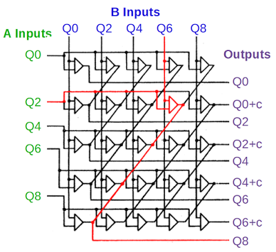
The circuit below adds the quinary parts of the two numbers and can be considered the "meat" of the adder. The qui part from the A register is on the left, the qui part from the B register is on the top, and the qui output is on the right. The outputs with "+c" indicate a carry if the result is 10 or more. The addition logic is implemented with a "brute force" matrix, connecting each pair of inputs to the appropriate output. An example is Q2 + Q6, shown in red. If these two inputs are set, the indicated AND gate will trigger the Q8 output.[10]

The quinary addition circuit in the IBM 1401 mainframe. This adds the quinary parts of two qui-binary digits. Highlighted in red is the addition of Q2 and Q6 to form Q8.

The quinary addition circuit in the IBM 1401 mainframe. This adds the quinary parts of two qui-binary digits. Highlighted in red is the addition of Q2 and Q6 to form Q8.

In the photo below, we can find the exact card in the IBM 1401 that performs this addition. The card in the upper left marked with a red asterisk computes the output Q8.[11]

The SMS cards in the IBM 1401 that perform arithmetic.

The SMS cards in the IBM 1401 that perform arithmetic.

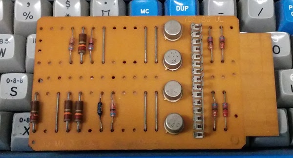
The circuitry in the IBM 1401 is simple enough that you can follow it all the way to the function of individual transistors.[12] The asterisk-marked card is a 3JMX SMS card containing 4 AND gates, and is shown below. Each of the round metal transistors corresponds to one AND gate for one of the sums that generates the output Q8. The top transistor is activated by inputs 8+0, the next for 0+8, the next 6+2, and the bottom one 2+6. Thus, the bottom transistor corresponds to the red AND gate in the schematic above.[13]

The SMS card of type 3JMX has four AND gates.

The SMS card of type 3JMX has four AND gates.

Qui-binary to BCD translation

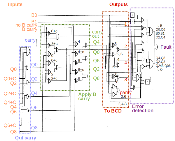
The diagram below shows the remainder of the qui-binary adder, which combines the qui and binary parts of the output, converts the output back to BCD, and detects errors. I'll just give an overview here, with more explanation in the footnotes.[14] The qui-binary carry circuit, in the blue box, processes the carry signals from the adder circuit. The next circuit, in the green box, applies any carry from the B bits, incrementing the qui component if necessary. The translation circuit, in red, converts the qui-binary result to BCD, using AND-OR logic. It also generates the parity output used for error detection in memory. The final circuit, in purple, is the error detection circuit which verifies the qui-binary result is valid and halts the computer if there is a fault.

The circuitry in the IBM 1401 mainframe to convert a qui-binary sum to a BCD result.

The circuitry in the IBM 1401 mainframe to convert a qui-binary sum to a BCD result.

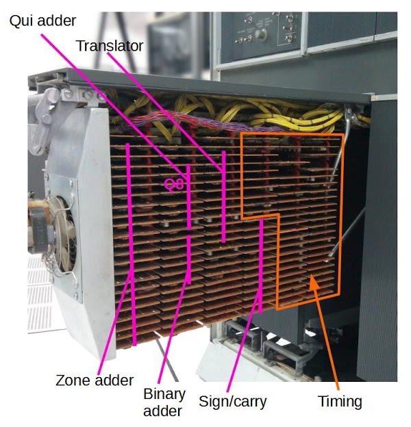
The photo below shows the functions of the different cards in the arithmetic rack.[15] The cards in the left half perform arithmetic operations. Each function takes multiple cards, since a single SMS card has a small amount of circuitry. "Q8" indicates the card discussed earlier that computes Q8. The right half is taken up with clock and timing circuits, which generate the clock signals that control the 1401.

This rack of circuitry in the IBM 1401 contains arithmetic logic (left) and timing circuitry (right).

This rack of circuitry in the IBM 1401 contains arithmetic logic (left) and timing circuitry (right).

Conclusion

This article has discussed how the 1401 adds or subtracts a single digit. The complete addition/subtraction process in the 1401 is even more complex because the 1401 handles numbers of arbitrary length; the hardware loops over each digit to process the entire numbers.[16][17]

Studying old computers such as the IBM 1401 is interesting because they use unusual, forgotten techniques such as qui-binary arithmetic. While qui-binary arithmetic seems strange at first, its error-detection properties made it useful for the IBM 1401. Old computers are also worth studying because their circuitry can be thoroughly understood. After careful examination, you can see how arithmetic, for instance, works, down to the function of individual transistors.

Thanks to the 1401 restoration team and the Computer History Museum for their assistance with this article. The IBM 1401 is regularly demonstrated at the Computer History Museum, usually on Wednesdays and Saturdays (schedule), so check it out if you're in Silicon Valley.

Notes and references

[1] Qui-binary is the opposite of bi-quinay encoding used in abacuses and old computers such as the IBM 650. In bi-quinary, the bi part is 0 or 5, and the quinary part is 0, 1, 2, 3, or 4.

[2] You might wonder why IBM didn't just use parity instead of qui-binary numbers. While parity detects bit errors, it doesn't work well for detecting errors during addition. There's no easy way to figure out what the parity should be for a sum.

[3] The IBM 1401 has hardware to multiply and divide numbers of arbitrary length. The multiplication and division operations are based on repeated addition and subtraction, so they use the qui-binary addition circuit, along with qui-binary doublers.

[4] The logic diagrams are all from the 1401 Instructional Logic Diagrams (ILD). Pages 25 and 26 show the addition and subtraction logic if you want to see the diagrams in context.

[5] The IBM 1401 performs operations on memory locations and the A and B registers provide temporary storage for digits as they are read from core memory. They are not general-purpose registers as in most microprocessors.

[6] A few more details about the console display. The "C" bit at the top of each register is the check (parity) bit used for error detection. The 1401 uses odd parity, so if an even number of bits are set, the C bit is also set. The "M" bit at the bottom is the word mark, which indicates the end of a variable-length field. The machine opcode character is zone B + zone A + 1, which indicates the letter "A".

Unlike modern computers, the 1401 uses intuitive opcodes so "A" means add, "S" means subtract, "B" means branch and so forth. (This is the actual opcode in memory, not the assembly mnemonic.) In the lower right, the mode knob is set to "Single cycle process", which allowed me to step through the instruction to get this picture. Normally this knob is set to "Run" and the console flashes frantically as instructions are executed.

[7] One surprising feature of the BCD translator is that it accepts binary inputs from 0 to 15, not just "valid" inputs 0 to 9. Input 10 is treated as 0, since the 1401 stores the digit 0 as decimal 10 in core. Values 11 through 15 are treated as 3 through 7. Thus, every binary input results in a valid (but probably unexpected) qui-binary value. As a result, the 1401 can perform addition on non-decimal characters, but the results aren't very useful.

[8] The IBM 1401 uses 9's complements since it is a decimal machine, unlike modern binary computers which use 2's complements. For example, the complement of 1 is 8, and the complement of 4 is 5. To subtract a number, the 9's complement of each digit is added (along with a carry). An example of using complements for subtration is 432 - 145. The 9's complement of 145 is 854. 432 + 854 + 1 = 1287. Discarding the top digit yields the desired result 432 - 145 = 287. Complements are explained in more detail in Wikipedia.
[9] If you trace through the AND-OR logic in the complement circuit, you can see that each pair of AND gates and and OR gate forms a multiplexer, selecting one input or the other. For example for the B1 output: if complement is 0 AND B1 is 1, the output is 1. OR, if complement is 1 AND B0 is 1, the output is 1. In other words, the output matches the B1 input if complement is 0, and matches the B0 input if complement is 1. The box labeled I in the schematic is an inverter.

[10] The quinary adder is implemented using wired-OR logic. Instead of an explicit OR gate, the AND outputs are simply wired together to produce the OR output. While the quinary adder looks symmetrical and regular in the schematic, its implementation uses three different SMS cards: 3JMX and 4JMX AND/OR gates, and JGVW AND gates, depending on the number of AND gates feeding the output.

[11] One component of interest in the photo of SMS cards is the silver rectangle on the lower right card. This is the quartz crystal that generates timing for the 1401. The SMS card is type RK, and the crystal runs the 347.5kHz oscillator. Eight oscillator half-cycles make up the 11.5 microsecond cycle time of the 1401. At the top of the photo are the wiring bundles connecting these circuits to other parts of the computer.

[12] Due to the simplicity of the IBM 1401 compared to modern computers, it's possible to understand how the IBM 1401 works at every level all the way to quantum physics. I'll give an outline here. The gates in an SMS card use a simple form of logic called CTDL by IBM and DTL (Diode-Transistor Logic) by the rest of the world. The 3JMX card schematic shows that each input is connected through a diode to the output transistor. If any input is high, current flows through the diode and turns off the transistor. The result is an AND gate (with inverted inputs). IBM Transistor Component Circuits (page 108) explains this circuit in detail.

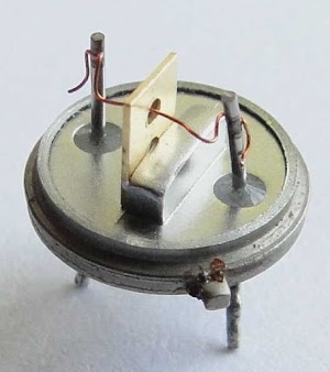
Going deeper, we can look inside the transistor. The board uses type 034 germanium alloy-junction transistors (details, details), very different from modern silicon-based planar transistors. These transistors consist of a germanium crystal base with indium beads fused on either side to form the emitter and collector. The regions of germanium-indium alloy form the "P" regions. In the photo, the germanium disk is in the small circular hole. Copper wires are connected to the indium beads. The photo below shows an IBM 083 transistor from the IBM 1401. This is the NPN version of the transistors in the 3JMX card. If you want a deeper understanding, look at bipolar junction transistor theory, which in turn is explained by quantum physics and solid-state device theory.

Inside a germanium alloy-junction transistor used in the IBM 1401 computer. This is an IBM 083 NPN transistor. Photo from http://ibm-1401.info/GermaniumAlloy.html

Inside a germanium alloy-junction transistor used in the IBM 1401 computer. This is an IBM 083 NPN transistor. Photo from IBM 1401 restoration team.

[13] You may wonder how 8=4+4 gets computed, since the card described doesn't handle that. The sum 4+4 is computed by the card just below the asterisk (a triple AND gate card of type JGVW). The other two AND gates in that card compute 6+6 and 8+8. To determine what each board in the IBM 1401 does, look at the Automated Logic Diagrams, page 34.32.14.2.

[14] The qui-binary carry logic happens in several phases. The qui parts are added, generating a carry if needed. The binary parts are added with a simple binary adder (not shown). A carry from the binary part shifts the qui part by 2. A carry out signal is also generated as needed. For instance, adding 3 + 5 is done by adding Q2 B1 + Q4 B1. This generates Q6 + B0 + B carry. The B carry increments the qui component to Q8, yielding the result Q8 B0 (i.e. 8).

The qui-binary to BCD translation circuit uses straightforward AND-OR logic, detecting the various combinations. Note that 0 is represented in the 1401 as binary 1010 (because binary 0000 indicates a blank), so the BCD output bits 8 and 2 are set for qui-binary value Q0 B0. The parity output is generate by combining the binary parity (even for B0; odd for B1) with the qui parity value. The qui even parity signal is set for Q0 or Q6, while the qui odd parity signal is set for Q2, Q4, Q8. Note that representing 0 as binary 1010 instead of 0000 doesn't affect the parity.

The error detection circuit uses AND-OR logic to detect bad qui-binary results. It detects a fault if no B bits are set or both B bits are set. Instead of testing every qui bit combination, it implements a short cut from the qui parity circuit. If the even qui parity signal and the odd qui parity signal are both set, this indicates multiple qui lines are set, triggering a fault. If neither qui parity signal is set, then no qui lines are set, also triggering a fault. The parity check misses a few qui combinations (such as Q0 and Q6 set), so these are tested separately. The result is that any invalid qui-binary result triggers a fault.
[15] The rack of cards shown is officially known as gate 01B3. The functions assigned to each card in the photo are approximate, because some cards are used by multiple functions. For exact information, see the plug list, which specifies the card type and function for every card in the 1401.
[16] One complication with the 1401's arithmetic instructions are numbers are stored as a positive value with a sign bit (on the last digit). This format makes printing of positive and negative numbers simpler, which is important for a business computer, but it makes arithmetic more complicated. First, the signs must be checked to determine if the numbers are being added or subtracted. Next, each digit is added or subtracted in sequence until the end of the number is reached. If the result is negative, the 1401 flips the result sign and converts the answer back to a positive value by making two additional digit-by-digit passes over the number. Modern computers use binary and handle negative numbers with two's complement, which makes subtraction much simpler. It takes 9 pages of documentation to explain the addition operation, complete with multiple flowcharts: see IBM 1401 Data Flow pages 24-32. (Keep in mind that these flowcharts are implemented in hardware, not with microcode or subroutines.)

[17] Arithmetic on the 1401 and the qui-binary adder are discussed in detail in 1401 Instruction Logic, pages 49-67. For the history leading up to qui-binary arithmetic, see this article by Carl Claunch.

Fixing the core memory in a vintage IBM 1401 mainframe

I recently had the chance to help fix one of the vintage IBM 1401 computer systems at the Computer History Museum when its core memory started acting up. As you might imagine, keeping old mainframes running is a difficult task. Most of the IBM 1401 restoration and repairs are done by a team of retired IBM engineers. But after I studied the 1401's core memory system in detail, they asked if I wanted to take a look at a puzzling memory problem: some addresses ending in 2, 4 or 6 had started failing.

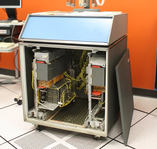
An IBM 1401 mainframe computer at the Computer History Museum. Behind it is the IBM 1406 Storage Unit, providing an additional 12,000 characters of storage. IBM 729 tape drives are at the right and an IBM 1402 Card Read Punch is at the far left.

An IBM 1401 mainframe computer at the Computer History Museum. Behind it to the left is the IBM 1406 Storage Unit, providing an additional 12,000 characters of storage. IBM 729 tape drives are at the right and an IBM 1402 Card Read Punch is at the far left.

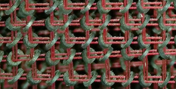
The IBM 1401 was low-end business computer that became the most popular computer of the early 1960s due to its low cost: $2500 a month, Like most computers of its era it uses ferrite core memory, which stores bits on tiny magnetized rings. The photo below shows a closeup of the ferrite cores, strung on red wires.

Closeup of the core memory in the IBM 1401 mainframe, showing the tiny ferrite cores.

Closeup of the core memory in the IBM 1401 mainframe, showing the tiny ferrite cores.

The 1401 had only 4,000 characters of storage internally, but could hold 16,000 characters with the addition of the IBM 1406 Storage Unit. This core memory expansion unit was about the size of a dishwasher and was connected to the 1401 computer by two thick cables.[1] This 12,000 character expansion box could be leased for $1575 a month or purchased for $55,100. (In comparison, a new house in San Francisco was about $27,000 at the time.) The failing memory locations were all in the same 4K block in the IBM 1406, which helped narrow down the problem.

A view inside the IBM 1406 Storage Unit, which provides 12,000 characters of storage for the IBM 1401 mainframe. At the left is the 8,000 character core module below the cards that control it.

A view inside the IBM 1406 Storage Unit, which provides 12,000 characters of storage for the IBM 1401 mainframe. At the left is the 8,000 character core module below the cards that control it.
The 1406 contains two separate core memory modules: one with 8,000 characters and one with 4,000 characters. In the picture above, the 8K core module is visible on the left, while the 4K core module is out of sight at the back right. Associated with each core module is circuitry to decode addresses, drive the core module, and amplify signals from the module; these circuits are in three rows of cards above each module. The 1406 also provided an additional machine opcode (Modify Address) for handling extended addresses. Surprisingly, the logic for this new opcode is implemented in the external 1406 box (the cards on the right), not in the 1401 computer itself. The 1406 box also contains hardware to dump the entire contents of memory to the line printer, performing a core dump.

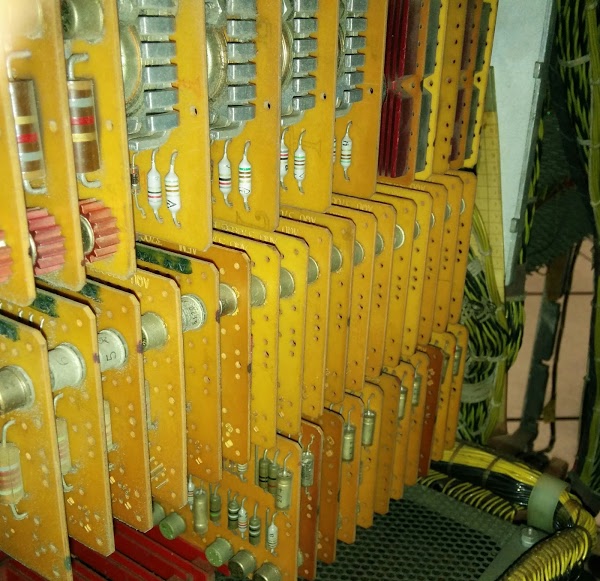
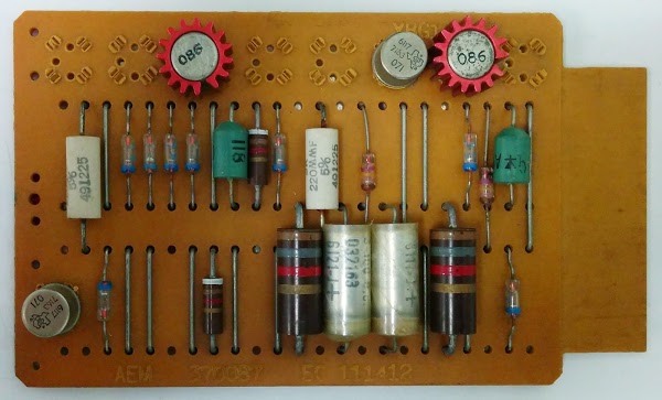
The circuits in the 1406 (and the 1401) are made up of Standardized Module System (SMS) cards. A typical card has a few transistors and implements a logic gate or two. Unlike modern transistors, these transistors are made from germanium, not silicon. The photo below shows rows of SMS cards inside the 1406. Note the metal heat sinks on the high-current transistors driving the core module.

A closeup of SMS cards inside an IBM 1406 Storage Unit. The top cards have heat sinks on high-current driver transistors.

A closeup of SMS cards inside an IBM 1406 Storage Unit. The top cards have heat sinks on high-current driver transistors.
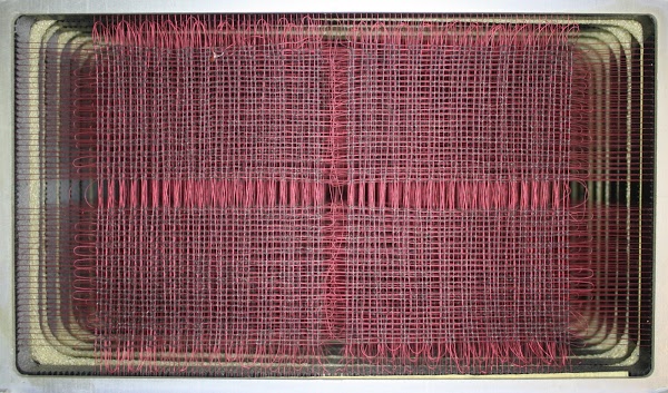
The core memory is made from planes of 4,000 cores, as seen below. Each plane is built from a grid of 50 by 80 wires, with cores where the wires cross. By simultaneously energizing one of the 50 horizontal (X) wires and one of the 80 vertical (Y) wires, the core at the intersection of the two wires is selected. Each plane holds one bit of each character, so 8 planes are stacked to hold a full character.

Core memory in the IBM 1401 mainframe. Each layer (plane) has 4,000 tiny cores in an 80x50 grid. Multiple planes are stacked to form the memory.

Core memory in the IBM 1401 mainframe. Each layer (plane) has 4,000 tiny cores in an 80x50 grid. Multiple planes are stacked to form the memory.
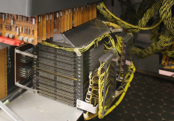
The photo below shows the 8K memory module inside the 1406, built from a stack of 16 core planes. (Since a stack of 8 planes makes 4K, 16 planes make 8K.) Mounted on the right of the core module are the "matrix switches", which drive the X and Y select lines; my previous core memory article explains them.

The 8,000 character core memory in the IBM 1406 Storage Unit consists of 16 layers (planes) of cores wired together. The matrix switches at the right (behind plastic) drive the control lines.

The 8,000 character core memory in the IBM 1406 Storage Unit consists of 16 layers (planes) of cores wired together. The matrix switches at the right (behind plastic) drive the control lines.
The IBM 1401 is a decimal machine and it uses 3-digit decimal addresses to access memory. The obvious question is how can it access 16,000 locations with a 3-digit address. To understand that requires a look at the characters used by the IBM 1401.

The IBM 1401 predates 8-bit bytes, and it used 6-bit characters. Each character consisted of a 4-bit BCD (binary-coded decimal) digit along with two extra "zone" bits. By setting zone bits, letters and a few symbols could be stored. For instance, with both zone bits set, the BCD digit values 1 through 9 corresponded to the characters "A" through "I". Other zone bit combinations provided the rest of the alphabet. While this encoding may seem strange, it maps directly onto IBM punched cards, which have 10 rows for the digit and two rows for zone punches. This encoding was called BCDIC (Binary-Coded Decimal Interchange Code), and later became the much-derided EBCDIC (Extended BCDIC) encoding. (You may have noticed that 8 planes are used for 6-bit characters. One extra plane holds special "word mark" bits, and the other holds parity.)

The point of this digression into IBM character encoding is that a three-digit address also included 6 zone bits. Four of these bits were used as part of the address, allowing 16,000 addresses in total.[2] For example, the address 14,578 would be represented as the digits 578 along with the appropriate zone bits, so the resulting address would be represented as the three characters "N7H".[3]

Getting back to the problem with the memory unit, the 4K bank was failing with addresses ending in 2, 4 and 6. Looking at 2, 4 and 6, I immediately concluded that what these all had in common was the 2 bit was set. Except 4 doesn't have the 2 bit set. So maybe the problem was with even addresses. Except 0 and 8 worked. After staring at bit patterns a while, I became puzzled because 2, 4 and 6 didn't really have anything in common.

Looking at the logic diagrams reveals the hardware optimization that makes 2, 4, and 6 have something in common. Since the problem happened with specific unit digits, the problem was most likely in the address decoding circuitry that translates the unit digit to a particular select line.[4] The normal way of decoding a digit is to look at the 4 bits of the digit to determine the value. Unexpectedly, the decoder only looks at 3 bits; this reduces the hardware required, saving money. For instance, the digit 2 is detected below if the 4 bit is clear, the 1 bit is clear, and the 8 bit is clear. The digit 4 is detected if the parity (CD) bit is clear, the 4 bit is set, and the 1 bit is clear. The digit 6 is detected if the 1 bit is clear, the 2 bit is set, and the 4 bit is set.[5] Looking at the decode logic, decoding of the digits 2, 4, and 6 (and only these digits) tests that the 1 bit is clear. Now the failure starts to make sense. If something is wrong with the units 1-bit-clear signal, these digits would not be decoded properly and memory would fail in the way observed.

The Instructional Logic Diagrams (ILD) for the IBM 1401 explain the circuitry of the computer. The above diagram shows the address decode logic used for the core memory.

The Instructional Logic Diagrams (ILD) for the IBM 1401 explain the circuitry of the computer. The above diagram shows part of the address decode logic used for the core memory.
The next step was to figure out how the units 1-bit-clear signal could be wrong. You'd expect a failure of one address bit to be catastrophic, not just limited to one memory bank. Looking at the specifics of the decoder circuitry revealed the problem.

Every connection and circuit of the IBM 1401 is documented in an Automated Logic Diagram (ALD). These diagrams were generated by computer and put in a set of binders for use by service engineers. The code number 42.73.11.2 on the previous diagram provides the page number of the related ALD. While these diagrams are extremely detailed, they are nearly incomprehensible. Since I'm using copies of reduced 50-year-old line printer output, the ALDs are also barely readable.

The Automated Logic Diagrams (ALD) for the IBM 1401 mainframe computer consist of hundreds of pages that show every card and connection in the computer. The above diagram shows part of the address decode circuitry in the IBM 1406 Storage Unit.

The Automated Logic Diagrams (ALD) for the IBM 1401 mainframe computer consist of hundreds of pages that show every card and connection in the computer. The above diagram shows part of the address decode circuitry in the IBM 1406 Storage Unit.
The diagram above shows part of the ALD for the units memory address decoding. Each box corresponds to a logic component on an SMS card and the lines show the wiring between cards. At the bottom of each box, "AEM-" indicates the type of SMS card. The reference information for an AEM/AQU card reveals that it is a Switch Decode card with two circuits. Each circuit combines an inverter, a three-input AND gate, and a high-current driver.[6]

Now we can see the root cause of the problem. The unit address bit 1 (highlighted in red on the ALD) goes into pin A of the Units 4 card and is inverted. The inverted value (pin D, yellow) then goes to the Units 2 and Units 6 cards, generating the decode outputs (green). If something is wrong with this signal, addresses 2, 4, and 6 won't decode, which is exactly the problem encountered. Thus, the Units 4 card seemed like the problem.

This IBM Standard Modular System (SMS) card is used by the core memory to decode addresses. It has two high-current outputs, driven by the germanium transistors at the top with red heat sinks.

This IBM Standard Modular System (SMS) card is used by the core memory to decode addresses. It has two high-current outputs, driven by the germanium transistors at the top with red heat sinks. The card type "AEM" is stamped into the bottom left of the card.
The diagram above indicates that the Units 4 card is card E15 in rack 06B5, which is in the right rear of the 1406 unit.[7] Once I'd located the right rack, I needed to find card E15. The three rows of cards are D through F (top). I counted to position 15 of 26 in row E. The photo below shows the position of the card (red arrow).

Circuitry inside the IBM 1406 Storage Unit. The green arrow indicates the 4,000 character core memory. The cards above it control the memory. The top row of cards has high-current drivers for the memory. The cards in the middle row decode addresses. The bottom row contains amplifiers to read the signals from the memory. The red arrow indicates the position of the faulty card. The fan above the cards provides cooling airflow. At the right, colorful wire bundles connect the circuitry.

Circuitry inside the IBM 1406 Storage Unit. The green arrow indicates the 4,000 character core memory. The cards above it control the memory. The top row of cards has high-current drivers for the memory. The cards in the middle row decode addresses. The bottom row contains amplifiers to read the signals from the memory. The red arrow indicates the position of the faulty card. The fan above the cards provides cooling airflow. At the right, colorful wire bundles connect the circuitry.

One convenient thing about the IBM 1401 and its peripherals is they are designed for easy maintenance. In many cases, you don't even need any tools. To get inside the IBM 1406, you just pop the front or side panels off (as shown below). The SMS cards have a metal cover to guide the cooling airflow, but that just pops off too. It's easy to attach an oscilloscope to see what's happening, although I didn't need to do that. The SMS cards themselves are easily pulled from their sockets. I'm told you don't even need to power down the system to replace cards, but of course I turned off the power.

Inside the IBM 1406 Storage Unit. At the left are the power supplies, including a 450W ferro-resonant regulator. The 8K core memory is at the right, connected by yellow wire bundles to the control circuitry above.

Inside the IBM 1406 Storage Unit. At the left are the power supplies, including a 450W ferro-resonant regulator. The 8K core memory is at the right, connected by yellow wire bundles to the control circuitry above.

I pulled out the card in slot E15, plugged in a replacement card from the 1401 lab's collection, and powered up the system. Much to my surprise, the memory worked perfectly after replacing the card. Some of the engineers (Stan, Marc, and Dave) tested the transistors on the bad card but didn't find any problems. After cleaning the bad card and swapping it back, the memory still worked, so there must have been some dirt or corrosion making a bad connection. They say this is the first problem they've seen due to bad connections, so the thick gold plating on the SMS card contacts must work well.

Conclusion

It's not every day one gets the chance to help fix a 50 year old mainframe, so it was an interesting experience. I was lucky that this problem turned out to be easy to resolve. The guys repairing the tape drives and card reader have much harder problems, since those devices are full of mechanical parts that haven't aged well.

Thanks to the members of the 1401 restoration team and the Computer History Museum for their assistance. Special thanks to Stan Paddock, Marc Verdiell and Dave Lion for inviting me to investigate this problem.

The IBM 1401 is demonstrated at the Computer History Museum on Wednesdays and Saturdays (unless there is a hardware problem) so check it out if you're in Silicon Valley (schedule).

Notes and references

[1] The 1406 expansion unit was 29" wide, 30 5/8" deep and 39 5/8" high and weighed 350 lbs. The 10 foot cables between the 1401 computer and the 1406 storage unit are each 1 1/4" thick; one provides power and the other has signals. The 1406 generates 250 watts of heat, which is less than I would have expected. Details are in the installation manual.

[2] The three-digit address has six zone bits in total. Four are used as part of the address. The other two zone bits to indicate an indexed address using one of three index registers (which are actually part of core, not separate registers). Indexed addressing was part of the "Advanced Programming" option which cost an extra $105 per month.

[3] For full information on converting addresses to characters, see the IBM 1401 Pocket Reference Manual, page 3.

[4] Scans of the Instructional Logic Diagrams (ILDs) are available online. The memory decode circuits are on page 56. Scans of the Automated Logic Diagrams (ALDs) are also available online; the core memory is in section 42.

[5] The IBM 1401 predates standardized logic symbols, so the logic diagram symbols may be confusing: the triangular symbol is an AND gate. The SWD (Switch Decode) card inverts its inputs, but that isn't shown on the logic diagram.

There are few subtleties in the decoding logic. You might think that the circuit described would decode a 0 digit as a 2 digit since the 1, 4, and 8 bits are clear. However, the IBM 1401 stores the digit 0 as the value 10 (8 bit and 2 bit set), since a blank is stored with all bits clear.

For the decoding using the parity bit, note that the IBM 1401 uses odd parity. For instance, the digit 4 (binary 0100) already has odd parity, so the CD (check digit) parity bit is clear. The digit 5 (binary 0101) has the CD parity bit set so three bits are set in total.

[6] The original idea of SMS cards was to build computers from a small set of standardized cards, but as you can guess from the complexity of the AEM card, engineers created highly-specialized SMS cards for specific purposes. IBM ended up with thousands of different SMS card types, defeating the advantages of standardization. I've created an SMS card database that describes a thousand different SMS cards.

[7] The 06B5 designation indicates which gate holds the card. (Each rack of cards is called a "gate" in IBM terminology. Confusingly, this has nothing to do with a logic gate.) The 06 indicates the 1406 frame. The B indicates a lower frame. Position 5 is in the back right. The same numbering system is used in the IBM 1401 itself. The 1401 is built around the same frame structure as the 1406, except with four frames, stacked 2x2. The left frames are numbered 01, and the right frames are 02. The frames on top are A, and the frames on the bottom are B. Gates 1 through 4 are in the front, and 5 through 8 continue around the back. A typical 1401 gate identifier is "01B2", which indicates the rack on the front of the 1401 below the console. (The use of frames to build computers and peripherals led to the term "main frame" to describe the processing unit itself.)