12-minute Mandelbrot: fractals on a 50 year old IBM 1401 mainframe

When I found out that the Computer History Museum has a working IBM 1401 computer[1], I wondered if it could generate the Mandelbrot fractal. I wrote a fractal program in assembly language and the computer chugged away for 12 minutes to create the Mandelbrot image on its line printer. In the process I learned a bunch of interesting things about the IBM 1401, which I discuss in this article.

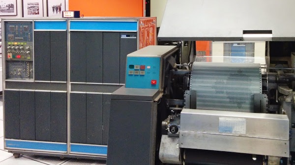
The IBM 1401 at the Computer History Museum printing the Mandelbrot fractal on the 1403 printer.

The IBM 1401 mainframe computer (left) at the Computer History Museum printing the Mandelbrot fractal on the 1403 printer (right). Note: this is a line printer, not a dot matrix printer.

The IBM 1401 computer was announced in 1959, and went on to become the best-selling computer of the mid-1960s, with more than 10,000 systems in use. The 1401 leased for $2500 a month[2] (about $20,000 in current dollars), a low price that let many more companies use computers. Even a medium-sized business could use the 1401 for payroll, accounting, inventory, order processing, invoicing, analysis, and many other tasks. The 1401 was called the Model-T of the computer industry due to its low price and great popularity.[3] Even for its time, IBM 1401 only had moderate performance, especially compared to a high-end business computer like the IBM 7080 (rental fee: $48,000 a month).[2] But the IBM 1401 became hugely popular because of its affordability, reliability, ease of use, high-quality printer and stylish appearance[4].

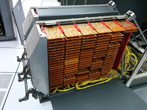
The 1401 was an early all-transistorized computer. These weren't silicon transistors, though, they were germanium transistors, the technology before silicon. The transistors and other components were mounted on circuit boards about the size of a playing card. These boards were called Standard Modular System (SMS) boards and each one provided a function such as a flip flop or simple logic functions. The IBM 1401 could contain thousands of SMS cards, depending on the features installed - the basic system had about 933 cards[5], while the system I used has 2881 SMS cards. (For more information on SMS cards, see my earlier article.)

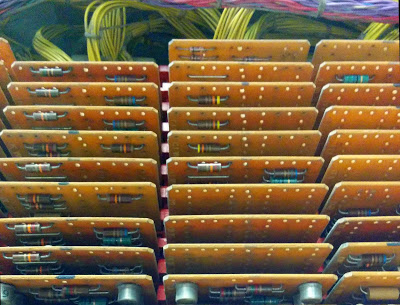
SMS cards inside the IBM 1401. These cards are part of the tape drive control, amplifying signals read from tape.

SMS cards inside the IBM 1401. These cards are part of the tape drive control, amplifying signals read from tape.

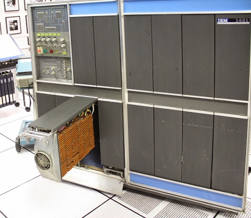
The SMS cards plug into racks (which IBM confusingly calls "gates"), that fold out from the computer as shown below. The 1401 is designed for easy maintenance - to access a gate, you just grab the handle and it swings out from the computer, exposing the wires and boards for maintenance. At the bottom of the gate, wiring harnesses connect the gate to other parts of the computer.[6] There are 24 of these gates in total.

The IBM 1401 computer is built from thousands of SMS circuit cards. This open rack (called a gate) shows about 150 SMS cards.

The IBM 1401 computer is built from thousands of SMS circuit cards. This open rack (called a gate) shows about 150 SMS cards.

Unusual features of the IBM 1401

It's interesting to look at old computers because they do things very differently. Some of the unusual features of the IBM 1401 are that it used decimal arithmetic and 6-bit characters, it had arbitrary-length words, and additional instructions were available for a rental fee.

The IBM 1401 is based on decimal arithmetic, not binary. Of course it uses 0's and 1's internally, but numbers are stored as digits using binary coded decimal (BCD). The number 123 is stored as three characters: '1', '2', and '3'. If you add 7 and 8, you get the digit 1 and the digit 5. Addresses are in decimal, so storage is in multiples of 1000, not 1024: the system with 16K of memory stores exactly 16,000 characters. All arithmetic is done in base-10. So if you divide two numbers, the IBM 1401 does base-10 long division, in hardware.

The IBM 1401 does not use bytes.[9] Instead, it uses 6-bit BCD storage. Every character is stored as a 4-bit BCD digit with two extra bits called "zone bits", named A and B.[7] The two extra zone bits allow upper-case letters (and a few special symbols) to be stored, as well as digits.[8] Using a byte as the unit of operation didn't become popular until later with the IBM System/360; in the early 1960s, computers often used strange word sizes such as 13, 17, 19, 22, 26, 33, 37, 41, 45, and 50 bit words.[9]

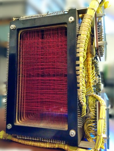
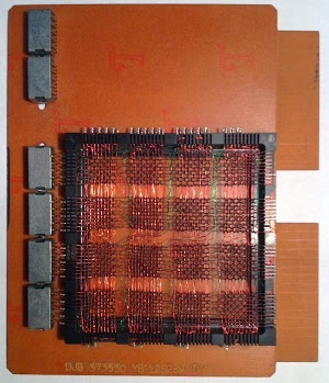
The photo below shows the core memory module from the IBM 1401, with 4,000 characters of memory. Each bit is stored in a tiny donut-shaped ferrite core with wires running through it. The core module is more complex than you'd expect, with 16 layers (frames) in total. Eight frames hold the 6 bits of data, plus the word mark bits (explained below) and parity bits. Six frames hold data from the card reader brushes and the print hammers, for data and error checking.[10] The remaining two frames are just used for wiring.

The 4000 character core memory module from the IBM 1401 computer.

The 4000 character core memory module from the IBM 1401 computer requires a huge amount of wiring.

Probably the most unusual feature of the 1401 is that it uses variable-length words, with word marks indicating each word. You might expect that variable-length words would let you use words of perhaps 8, 16, and 32 bits. But the IBM 1401 permitted words of arbitrarily many characters, up to the total size of memory! For instance, an instruction could move a 47-character string, or add 11-digit numbers. (Personally, I think it's easier to think of it as variable-length fields, rather than variable-length words.)

The word mark itself is a bit that is set on a memory location to indicate the boundary of a word (i.e. field).[11] An instruction on the IBM 1401 processes data through memory sequentially until it hits a word mark. It's important to remember that word marks are not part of the characters, but more like metadata, so they remain as new data records are read in and processed.[11] The main motivation behind variable-length words was to save expensive core memory, since each field length can be fit to the exact size required.

Another interesting thing about the IBM 1401 is that many instructions were extra-price options. The "advanced programming" feature provided new instructions for moving records, storing registers, and using index registers; this required the installation of 105 new SMS cards and (coincidentally) cost $105 a month. Even the comparison instruction cost extra. Because the 1401 uses BCD, you can't just subtract two characters to compare them as you would on most processors. Instead, the 1401 uses a bunch of additional circuitry for comparison, about 37 SMS cards for which you pay $75 a month.[12] Renting the printer buffer feature for $375 a month added a separate core storage module, 267 more SMS cards, and two new instructions. The bit test instruction cost only $20 a month and additional card punch control instructions were $25 a month. If you bought one of these features, an IBM engineer would install the new cards and move some wires on the backplane to enable the feature. The wire-wrapped backplanes made it relatively easy to update the wiring in the field.

The 1401 could be expanded up to 16,000 characters of core memory storage: 4,000 characters in the 1401 itself, and 12,000 characters in a 1406 expansion box, about the size of a dishwasher. The 12K expansion sold for $55,100 (about $4.60 per character), or rented for $1,575 a month. (You can see why using memory efficiently was important.) Along with the expanded memory came additional instructions to manipulate the larger addresses.

The tiny magnetic cores providing storage inside the IBM 1401's 4,000 character memory.

The tiny magnetic cores providing storage inside the IBM 1401's 4,000 character memory. Wires pass through each core to read and write memory. You can see multiple layers of cores in this photo.

One feature that you'd expect a computer to have is a subroutine call instruction and a stack. This is something the 1401 didn't have. To call a subroutine on the IBM 1401, you jump to the start of the subroutine. The subroutine then stores the return address into a jump instruction at the end, actually modifying the code, so at the end of the subroutine it jumps back to the caller.[13] If you want recursion, you're on your own.

Some advanced features of the 1401

Compared to modern computers, the IBM 1401 is extremely slow and limited. But it's not as primitive as you might expect and it has several surprisingly advanced features.

One complex feature of the IBM 1401 is Editing, which is kind of like printf implemented in hardware. The Edit instruction takes a number such as 00123456789 and a format string. The computer removes leading zeros and inserts commas as needed, producing an output such as 1,234,567.89. With the optional Expanded Editing feature (just $20/month more), you can obtain floating asterisks (******1,234.56) or a floating dollar sign ($1,234.56), which is convenient for printing checks. Keep in mind that this formatting is not done with a subroutine; it is implemented entirely in hardware, with the formatting applied by discrete transistors.

Another advanced feature of the IBM 1401 is extensive checking for errors. With tens of thousands of components on thousands of boards, many things can go wrong. The 1401 catches malfunctions so they don't cause a catastrophe (such as printing million dollar payroll checks). First, the memory, internal data paths, instruction decode, and BCD conversion are all protected by parity and validity checks. The ALU uses qui-binary addition to detect arithmetic errors. The card reader reads each card twice and compares the results.[10] The 1401 verifies the printer's operation on each line. (The read, punch, and print checks use the additional core memory planes discussed earlier.) As a result, the 1401 turned out to be remarkably reliable.

Because the IBM 1401 has variable word length, it can perform arbitrary-precision arithmetic. For instance, it can multiply or divide thousand-digit numbers with a single instruction. Try doing that on your Intel processor! (I tried multiplying 1000-digit numbers on the 1401; it takes just under a minute.) Hardware multiply/divide is another extra-cost feature; to meet the 1401's price target, they made it an option with the relatively steep price of $325 per month. You do get a lot of circuitry for that price, though - about 246 additional SMS cards installed in two gates.[14] And remember, this is decimal multiplication and division, which is much more difficult to do in hardware than binary.

The 1401 I used is the Sterling model which it supports arithmetic on pounds/shillings/pence, which is a surprising thing to see implemented in hardware. (Up until 1971, British currency was expressed in pounds, shillings, and pence, with 12 pence in a shilling and 20 shillings in a pound. This makes even addition complicated, as tourists often discovered.) By supporting currency arithmetic in hardware, the 1401 made code faster and simpler.[15]

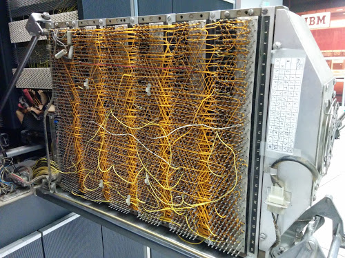
A maze of wire-wrapped wires connects the circuits of the IBM 1401 computer.

A maze of wire-wrapped wires on the back of a gate connects the circuits of the IBM 1401 computer. The wiring was installed by automated machinery, but the wiring could be modified by field engineers as needed.

Implementing the Mandelbrot in 1401 assembly language

Writing the Mandelbrot set code on the 1401 is a bit tricky since I did it in assembly language (called Autocoder). The hardest part was thinking about word marks. Another complication was the 1401 doesn't have native floating point arithmetic, so I used fixed point: I scaled each number by 10000, so I could represent 4 decimal places with an integer. The 1401 is designed for business applications, not scientific applications, so it's not well-suited for fractal generation. But it still got the job done.

The 1401 didn't need to be programmed in assembly language - it supports languages such as Fortran and COBOL - but I wanted the full 1401 experience. It does amaze me though that you can run a COBOL compiler on a machine with just 4,000 characters of memory. The Fortran compiler required a machine with 8,000 memory location; in order to fit, it ran in 63 separate phases.

The assembly language code for the Mandelbrot fractal is shown below. The first part of the code defines constants and variables with DCW. This is followed by three nested loops to loop over each row, each column, and the iterations for each pixel. Some of the instructions in the code are M (multiply), A (add), S (subtract), and C (compare). Comments start with asterisks.

               JOB  MANDELBROT
     *GENERATES A MANDELBROT SET ON THE 1401
     *KEN SHIRRIFF  HTTP://RIGHTO.COM
               CTL  6641
               ORG  087
     X1        DCW  001  *INDEX 1, COL COUNTER TO STORE PIXEL ON LINE
               ORG  333
     *
     *VALUES ARE FIXED POINT, I.E. SCALED BY 10000
     *Y RANGE (-1, 1). 60 LINES YIELDS INC OF 2/60*10000
     *
     YINC      DCW  333
     XINC      DCW  220          *STEP X BY .0220
     *
     *Y START IS -1, MOVED TO -333*30 FOR SYMMETRY
     *
     Y0        DCW  -09990       *PIXEL Y COORDINATE
     *
     *X START IS -2.5
     *
     X0INIT    DCW  -22000       *LEFT HAND X COORDINATE
     X0        DCW  00000        *PIXEL X COORDINATE
     ONE       DCW  001
     ZR        DCW  00000        *REAL PART OF Z
     ZI        DCW  00000        *IMAGINARY PART OF Z
     ZR2       DCW  00000000000  *ZR^2
     ZI2       DCW  00000000000  *ZI^2
     ZRZI      DCW  00000000000  *2 *ZR *ZI
     ZMAG      DCW  00000000000  *MAGNITUDE OF Z: ZR^2 + ZI^2
     TOOBIG    DCW  00400000000  *4 (SCALED BY 10000 TWICE)
     I         DCW  00           *ITERATION LOOP COUNTER
     ROW       DCW  01
     ROWS      DCW  60
     COLS      DCW  132
     MAX       DCW  24           *MAXIMUM NUMBER OF ITERATIONS
     *
     *ROW LOOP
     *X1 = 1  (COLUMN INDEX)
     *X0 = -2.2 (X COORDINATE)
     *
     START     LCA  ONE, X1     *ROW LOOP: INIT COL COUNT
               LCA  X0INIT, X0  *X0 = X0INIT
               CS   332         *CLEAR PRINT LINE
               CS               *CHAIN INSTRUCTION
     *
     *COLUMN LOOP
     *
     COLLP     LCA  @00@, I     *I = 0
               MCW  X0, ZR      *ZR = X0
               MCW  Y0, ZI      *ZI = Y0
     *
     *INNER LOOP:
     *ZR2 = ZR^2
     *ZI2 = ZI^2
     *IF ZR2+ZI2 > 4: BREAK
     *ZI = 2*ZR*ZI + Y0
     *ZR = ZR2 - ZI2 + X0
     *
     INLP      MCW  ZR, ZR2-6   *ZR2 =  ZR
               M    ZR, ZR2     *ZR2 *= ZR
               MCW  ZI, ZI2-6   *ZI2 =  ZI
               M    ZI, ZI2     *ZI2 *= ZI
               MCW  ZR2, ZMAG   *ZMAG = ZR^2
               A    ZI2, ZMAG   *ZMAG += ZI^2
               C    TOOBIG, ZMAG  *IF ZMAZ > 4: BREAK
               BH   BREAK
               MCW  ZI, ZRZI-6  *ZRZI = ZI
               M    ZR, ZRZI    *ZRZI = ZI*ZR
               A    ZRZI, ZRZI  *ZRZI = 2*ZI*ZR
               MCW  ZRZI-4, ZI  *ZI = ZRZI (/10000)
               MZ   ZRZI, ZI    *TRANSFER SIGN
               A    Y0, ZI      *ZI += Y0
               S    ZI2, ZR2    *ZR2 -= ZI2
               MCW  ZR2-4, ZR   *ZR = ZR2 (/10000)
               MZ   ZR2, ZR     *TRANSFER SIGN
               A    X0, ZR      *ZR += X0
     *
     *IF I++ != MAX: GOTO INLP
     *
               A    ONE, I      *I++
               C    MAX, I      *IF I != MAX THEN LOOP
               BU   INLP
               MCW  @X@, 200&X1  *STORE AN X INTO THE PRINT LINE
     BREAK     C    X1, COLS    *COL LOOP CONDITION
               A    ONE, X1
               A    XINC, X0    *X0 += 0.0227
               BU   COLLP
               W                *WRITE LINE
     *
     *Y0 += YINC
     *IF ROW++ != ROWS: GOTO ROWLP
     *
               C    ROW, ROWS   *ROW LOOP CONDITION
               A    ONE, ROW
               A    YINC, Y0    *Y0 += 0.0333
               BU   START
     FINIS     H    FINIS       HALT LOOP
               END  START

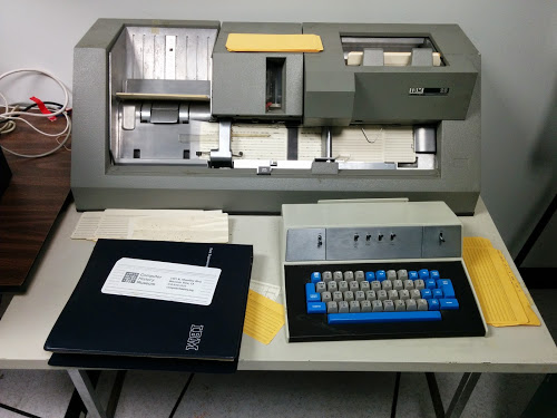
I compiled and ran the code with the ROPE compiler and simulator before using the real computer.[16] The cards were punched automatically by an IBM 029 keypunch controlled by a PC through a bunch of USB-controlled relays. The photo below shows the keypunch in operation. Each blank card drops down from the feeder in the upper right. The card is punched as it moves to the left. Punched cards are then flipped up and stacked in the upper left area (empty in this picture).

An IBM 029 keypunch preparing a card deck that generates the Mandelbrot fractal.

An IBM 029 keypunch preparing a card deck that generates the Mandelbrot fractal.

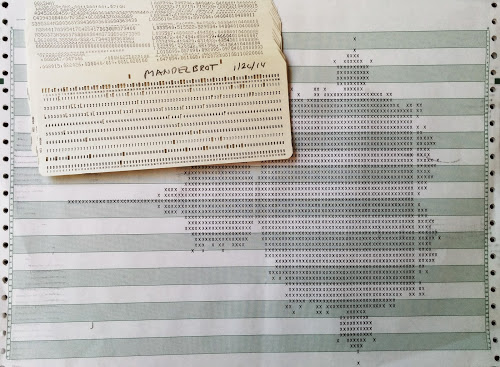
The resulting card deck is shown below, along with the output of execution. The program fits onto just 16 cards, but the card format is a bit unusual. The machine code for the Mandelbrot program is punched into the left half of the each card, with code such as M384417A395417. An interesting thing about the 1401 is the machine code is almost human-readable. M384417 means Move field from address 384 to address 417. A395417 means Add the number at address 395 to the number at address 417. The text on these cards is the actual machine code that gets executed, not the assembly code. Since the machine is character-based, not binary, there's no difference between the characters "428" and the address 428.

The card deck to generate the Mandelbrot fractal on the IBM 1401 computer.

The card deck to generate the Mandelbrot fractal on the IBM 1401 computer, along with the output. The white stripe through the fractal near the right is where a hammer in the printer malfunctioned.

If you look at the right half of the cards, there's something totally different going on, with text like L033540,515522,5259534. There's no operating system, so, incredibly, each card has code to copy its contents into the right place in memory (L instruction), add the word marks (, instruction), and load the next card. In other words, the right hand side of each card is a program that runs card-by-card to load into memory the program on the left hand side of the card deck, which is executed after the last card is loaded.[17]

To run the program, first you hit the "Power On" button on the IBM 1401 console. Relays clunk for a moment to power up the system and then the computer is ready to go (unlike modern computers that take so long to boot). You put the cards into the card reader and hit the "Load" button. The cards fly through the reader at the remarkable speed of 800 cards per minute so the Mandelbrot program loads in just over a second. The console starts flickering as the program runs, and every few seconds the line printer hammers out another line of the fractal. After 12 minutes of execution, the fractal is done. (Interestingly enough, the very first picture of a Mandelbrot set was printed on a line printer in 1978.[18])

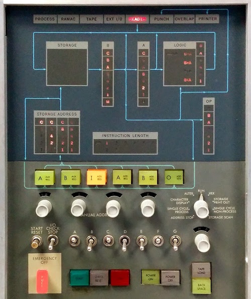
The console of an IBM 1401 mainframe.

The console of the IBM 1401 mainframe. The top half shows the data flow through the computer, from storage to the B and A registers and the logic unit. Each 6-bit value is displayed as 1248ABC, where A and B are zone bits and C is the check (parity) bit. On the right, "OP" shows the operation being executed. Below are knobs to manually access memory. On the left, the "Start Reset" button clears an error, such as the card read failures I would hit. At the bottom are the important buttons to turn the computer on and off. Note the Emergency Off handle that immediately cuts the power.

Conclusions

Writing a Mandelbrot program for the IBM 1401 was an interesting project. You think a bit differently about programming when using decimal numbers and keeping track of word marks. But I have to say that comparing the performance with a current machine - not to mention the storage capacity - makes me appreciate Moore's Law.

The Computer History Museum in Mountain View runs demonstrations of the IBM 1401 on Wednesdays and Saturdays. It's amazing that the restoration team was able to get this piece of history working, so if you're in the area you should definitely check it out. The schedule is here. Tell the guys running the demo that you heard about it from me and maybe they'll run my prime number program or Pi program. You probably wouldn't want to wait for the Mandelbrot to run.

Thanks to the Computer History Museum and the members of the 1401 restoration team, Robert Garner, Ed Thelen, Van Snyder, and especially Stan Paddock. The 1401 team's website (ibm-1401.info) has a ton of interesting information about the 1401 and its restoration.

Notes and references

[1] The Computer History Museum has two working 1401 computers: the "German 1401" and the "Connecticut 1401" (based on where they came from). I used the German 1401 since the Connecticut 1401 was undergoing card reader maintenance at the time.

[2] While the $2500 per month rental rate is quoted in many places, the price could climb to $10,000 a month for a full system with multiple tape drives. The price varied greatly depending on the 1401 model, the amount of memory, and the peripherals (tape drives, card reader, printer, disk drive). The minimal configuration (1401 Model A, 1402 card reader, and 1403 printer) went for $2,475 a month (or purchased for $125,600 - about $1 million accounting for inflation). A "recommended" configuration with 8K of memory, processor options, and another printer went for $4,610 a month. Tape drives boosted the price at $980 a month for the interface and $1100 a month for each 729 IV tape drive. A 4000 character memory expansion cost $575 per month.

Detailed information on 1961 computers including rental rates is available in an interesting survey of computers in 1961, the thousand-page A Third Survey of Domestic Electronic Digital Computing Systems", Report No. 1115, March 1961 (1401 page). The basic IBM rental price was for one 8-hour shift (176 hours a month). The computers included a time counter, and users were billed extra if they went over the allotted time. Customers often paid a higher rental fee so they could run 24/7.

[3] The comment that the 1401 became the Model-T of the computer industry is from the article IBM System/360, by IBM VP Bob Evans. One piece of trivia from that article is the IBM 1620 rented for $1600 a month, making it the first IBM system renting for a price less than its model number.

[4] The IBM 1401 has a very distinctive style, especially compared to earlier IBM computers (such as the 650 or 704) with a very utilitarian, industrial appearance. The sleek, modernist style of the 1401 isn't arbitrary, but the result of a detailed industrial design process. The book The Interface: IBM and the Transformation of Corporate Design has a very interesting discussion of the effort IBM put into industrial design. Edgar Kaufmann, Jr came up with important design ideas that were developed by Eliot Noyes. Some design concepts were recessed pedestals for a feeling of floating and lightness, the concealment of most of the circuitry, expressing the "inherent drama" of computers, the carefully controlled color scheme, and modern materials for the cabinets. The tape drives in particular were wildly successful at expressing the "inherent drama" of computing, to the point that spinning tape drives became a movie cliche (tvtropes: Computer Equals Tapedrive).

[5] The number of SMS cards in an IBM 1401 depends on the model, the options installed, engineering changes (i.e. fixes) applied to the system, and the amount of memory in use. I got the number 1206 by analyzing the SMS plug chart and counting 933 basic cards, 267 Sterling basic cards, 6 power supply cards, and 11 cards for storage support. This machine is the Sterling model, so it is slightly more complex than the regular model.

[6] The IBM 1401 has 32 "potential" gates: 16 on the front and another 16 on the back, but only 24 of these are gates with circuitry. The two potential panels in the upper left are taken up by the control panel, which swings out to reveal the core memory behind it. Four panels have power supplies behind them (although much of the power supply is inside the card reader, strangely). Two more spots are occupied by the surprisingly thick cables connecting the 1401 to peripherals. This leaves 24 swing-out gates; some may be unused, depending on the optional features installed.

[7] The zone bits are closely related to the zone punches in IBM punch cards. The top row of a punch card is the 12 (Y) zone, and the row beneath it is the 11 (X) zone. A number has one hole punched in the card row corresponding to the number (rows 0 through 9). A character usually has two holes punched: 1 through 9 for the BCD value, and a zone punch for the zone bits. The zone punch is card zone 11 for zone bit B set, card zone 12 for zone bits A and B, or card row 0 for zone bit A.

There are a few complications, though, that mess up this pattern. First, for characters outside the 0-9 range, two digit punches are used: 8 and the digit for the low three bits. (e.g. '#' is stored as bits 8, 2, and 1, so it is punched as 8 and 3.) Second, because card row 0 is used both for the digit 0 and as a zone punch, there is a conflict and the value 0 is treated as 10 in certain conditions (and punched as 8 and 2). Because a blank has no punches and is stored as 0 internally, the digit 0 is stored as 10. Different IBM systems treat these corner cases differently. Custom features were available for the 1401 to provide compatibility as needed.

[8] The zone bits are used for a few things in addition to letters. A zone bit is added to the low-order digit of a number to indicate the sign of the number. Memory addresses are expressed as three digits, which would allow access to 1000 locations; by using zone bits, the three digit address can reach 16,000 locations. The zone bits also track overflow in arithmetic operations.

[9] Originally byte referred to the group of bits used to encode a character, even if it wasn't 8 bits (see Planning a Computer System: Project Stretch, p40). Some examples of unusual word lengths: The RCA 601 supported 6, 8, 12, 16-bit, or variable-length words. SPEC used 13-bit words. The Hughes Airborne Computer used 17-bit words, while the Hughes D Pat used 19-bit words and the Hughes M 252 used 20-bit words. The RW 300 used 18-bit words, while the RW 400 used 26-bit words. The Packard Cell 250 used 22-bit words. UNIVAC 1101 used 24-bit words. ALWAC II used 32 bits plus sign (33 bits). COMPAC used 37 bits (36 + sign). AN/MJQ used 41-bit words. SEAC used 45 bits (44 plus sign). AN/FSQ 31 used 48 bit words. ORACLE used 50-bit words. The Rice University computer used 54-bit words. Details on these computers are in A Third Survey of Domestic Electronic Digital Computing Systems.

[10] The card reader reads each card twice and verifies that the hole count is the same for both reads. If the counts don't match, the card reader detects the error and stops. In more detail, each card is read "sideways", a row of 80 positions at a time. Two bits keep the status of each column. One bit is turned on if there is any hole. The other bit is toggled for each hole. (Thus, it's not exactly a count, simplifying the logic.) The process is reversed on the second read, so both bits will end up back at 0 for a correct read.

Since the next card is already getting read as the first card is getting verified, two sets of bits are needed, one for the first card and one for the second card. Thus, four planes of 80 bits each are used in total to verify card reads.

Each of the 240 brushes in the card reader has a separate wire that goes through a specific core in the 1401's core memory. Likewise, each of the 132 print hammers in the printer is wired directly to an individual core. Thus, there are thick cables containing hundreds of wires between the IBM 1401 and the card reader and the printer.

[11] There are several details of wordmarks I'll point out. The IBM 1401 is obviously big-endian, since that's how numbers are punched on cards. Since arithmetic operations need to start with the lowest-order digit, they start at the "end" of the number and work backwards through memory to the highest-order digit. The consequence is an instruction is given the address of the end of the field and progresses to lower addresses until it hits the word mark, which is at the beginning of the field. This seems backwards if you're a C programmer, where you start at the beginning of a string and go forwards until you hit the end.

Word marks are also used to indicate the start of each instruction. Instructions can be 1 to 8 characters long, and the presence of a word mark controls the length. Bootstrapping the word marks for the first instructions loaded into the computer requires some tricks.

[12] The comparison logic is more complex than you'd expect. Surprisingly, the comparison order doesn't match the binary order of characters. Also, comparisons aren't implemented with subtraction (like most processors). Instead, logic first determines if the characters are special characters or not - special characters are before regular characters (with some exceptions: for example, - is between I and J). Then a lot of AND-OR logic performs basically brute-force comparison by looking at various bit patterns. The results of a comparison can be seen on the control panel in the Logic box. The optional compare logic is shown on the Intermediate Level Diagrams (ILD), page 37.

[13] Self-modifying code, where the program changes its own instructions, was common in the past. A guide to IBM 1401 programming, 1961, has a whole chapter (6) on this, discussing how "we are able to operate on instruction in storage just as through they were data". Treating code as data wasn't done only by Lisp programmers. In fact, the book calls the ability of a program to modify itself "by all odds the most important single feature of the stored program concept." As well as subroutine returns, IBM 1401 programmers used self-modifying code for indexing, address computation, and complex conditional branching. On current machines, Self-modifying code is rare because it's harder to debug and messes up the instruction pipeline.

[14] For details on how the multiply and divide operations work internally, see the optional feature manual. This circuit has some complicated optimizations. For example, to speed up the repeated additions, it will add the doubled value instead if appropriate. But doubling a decimal value takes a fairly complicated circuit (unlike binary doubling, which is trivial). And there's error checking to make sure nothing goes wrong in the doubling.

[15] The Sterling circuitry to support £sd math is even more complicated because shillings and pence are stored in a compressed form. The obvious representation is a two-digit field for pence (0 to 11) and a two-digit field for shillings (0 to 19). But to save precious memory and storage space, the BSI standard and incompatible IBM standard use one-digit fields and special characters. A knob on the control panel selects which standard to use. The Sterling hardware must perform arithmetic on this compressed representation, as well as handling the non-decimal bases of shillings and pence.

This knob on the control panel of the IBM 1401 computer selects the storage mode for pence and shillings.

This knob on the control panel of the IBM 1401 computer selects the storage mode for pence and shillings.

[16] If you want to write a program for the 1401, instructions on using the ROPE simulator are here. It's a simple IDE that lets you edit assembly code (which is called Autocoder), assemble it, and then run it on the simulator. Take a look at A guide to IBM 1401 Programming and Programming the 1401 if you want to understand how to program the 1401. The 1401 Reference Manual is also useful for understanding what the instructions do.

[17] Each card also has a four-digit sequence number in the last columns. This lets you re-sort the cards if you happen to drop the deck and scramble the program.

[18] The first picture of the Mandelbrot set appears in 1978 paper by Brooks and Matelski, prior to Mandelbrot's work. (Thanks to Robert Garner for pointing this out.) There's some controversy over who "really" discovered the Mandelbrot set. See Who Discovered the Mandelbrot Set? in Scientific American for a discussion.
A database of SMS cards: The technology inside IBM's 1960s mainframes

IBM's mainframes of the 1960s are based on an interesting technology - Standard Modular System cards or SMS cards. These cards, created in the early years of transistorized computing, each implement a simple circuit on a board about the size of a playing card. You probably think of silicon as the basis for computers, but SMS cards use earlier transistors based on a semiconductor called germanium[1]. Eventually, of course, silicon took over, but in the early 1960s it was germanium not silicon that ran computers.

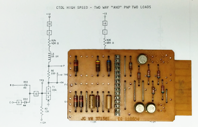
SMS cards were originally created for the IBM 7030 Stretch supercomputer.[2] The idea of SMS cards was to have a few standard cards that formed the building blocks that could be combined to build a computer. Each card provides a basic function such as a flip flop or a few logic gates. The board below, for example, implements three AND gates[3], using a relatively slow type of logic called diode-transistor logic that only requires one transistor per gate. You can see the transistors (silver circles) and diodes on the right, while resistors and inductors[4] are on the left.

This SMS card is used in the IBM 1401 for arithmetic. This card is a JGVW triple AND gate.

This SMS card is a JGVW triple AND gate. Note the card code "JG VW" is embossed in the lower left corner of the card.

SMS cards became the basis of of IBM's systems and were used on computers such as the IBM 1401, IBM 1620, and IBM 7000 series, as well as in tape drivers, printers, and other peripheral devices. SMS cards continued to be used well into the 1970s, even after integrated circuits made discrete transistors obsolete: advanced mainframes of the 1970s such as the IBM 370 still used multiple SMS cards for power supply regulation.
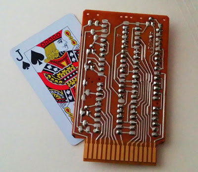
The picture below shows the back of an SMS card. The 16 gold-plated contacts on the end plug into a socket in the computer, connecting the card. The circuit board pattern is considerably more complex than necessary; depending on the components installed, one circuit board can implement several different SMS cards, reducing manufacturing costs.

An IBM SMS card (type DGU) with a playing card for scale.

An IBM SMS card (type DGU) with a playing card for scale.

Since each SMS card is so basic, it takes thousands of them to build a computer. The picture below shows an IBM 1401 mainframe, a very popular business computer of the 1960s. One of the racks of cards (which IBM confusingly calls a "gate") is open, showing more than 125 SMS cards plugged in. The circuitry in this specific gate below implements timing and logic functions (such as addition and subtraction). For maintenance, each gate swings out of the computer simply by pulling on the handle above the fan. The 1401 has 24 gates like this full of SMS cards, each one implementing different functionality of the computer. In total, the IBM 1401 computer contains more than 3400 SMS cards.

The IBM 1401 computer with gate 01B3 open, showing the timing and logic circuitry.

The IBM 1401 computer with gate 01B3 open, showing the SMS cards that implement timing and logic circuitry.

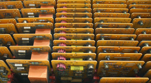
The picture below is a closeup of the SMS cards plugged into a gate in the IBM 1401. At the top of the gate, wiring harnesses connect this circuitry to other parts of the computer. On the back of each gate, the SMS cards are connected together by wirewrapping.

SMS cards installed in the IBM 1401 computer

SMS cards installed in the IBM 1401 computer

Although the original idea of SMS cards was to standardize on a few types, the number of different cards exploded as time went one, resulting in thousands of different SMS card types. As well as logic gates, SMS cards can have an amazing variety of functions such as an oscillator, voltage regulator, core memory, fuses, printer hammer driver, disk speed detector or temperature switch. The 1401 computer alone uses 162 different types of SMS cards.

This DJB double-width SMS card provides core memory storage in the IBM 1443 printer

This double-width SMS card provides core memory storage in the IBM 1443 printer. Photo courtesy of maisorbus.

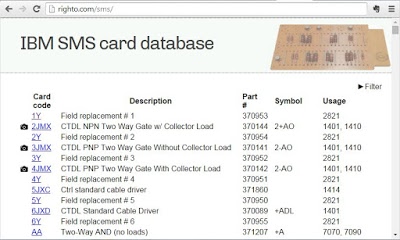
Information on particular SMS cards is surprisingly hard to find, so I made a database of SMS cards, collecting information on 900 different cards. Given the historical importance of SMS cards, I think information on this technology should be preserved. I pulled together information from scans of old IBM documents and a bunch of other sources (which was more work than I expected). You can access the database at righto.com/sms and see the wide variety of cards along with photos, descriptions, schematics, and the devices that use them.

Database of IBM SMS cards, click to access

In the 1960s, IBM made SMS cards by the millions, but most of them have been scrapped for the gold in their contacts.[5] You can still find a few SMS cards on places such as eBay[6], though, where they are collectables for about $15 each. If you want to see SMS cards in operation, the Computer History Museum in Mountain View has live demonstrations of the 1401 computer on Wednesdays and Saturdays (schedule). Check it out if you're in the area.[7]

In conclusion, SMS cards are an important part of computer history of the 1960s. It's hard to imagine computers before silicon, but SMS cards provide a window into that time. While the technology of today's computers is hidden away in microchips, the whole circuitry of older computers is exposed, letting you see how individual components make simple logic circuits, these boards are combined into functional units, and the computer is built from these units. And if technology had progressed slightly differently, this area might be known as Germanium Valley instead of Silicon Valley.

Notes and references

[1] For the first few years, transistors were made of germanium, not silicon. In 1954, silicon transistors were introduced and rapidly took over because they were more stable and had better operating characteristics. Germanium transistors are almost entirely obsolete now, but they still remain popular in fuzz and distortion pedals, where they are said to give a better sound than silicon transistors.
[2] The IBM 7030 Stretch supercomputer is described in detail in The engineering design of the Stretch Computer, 1959. The Stretch used 22,000 SMS cards, of which 4,000 were double cards. Stretch used just 42 different types of SMS cards (24 single-width and 18 double-width), with two types of cards making up more than half of the computer. In comparison, the IBM 1401 is a much smaller system with just 3047 total cards, but it has more than 120 different card types. Some cards can be modified by jumpers; counting the variants the 1401 has 162 different card types. (The 3047 figure is for the Computer History Museum's IBM 1401; the figure will vary for models with different optional features.)

[3] The JGVW SMS card has three two-input AND gates, running on -12V. Inputs are +6V or -6V, outputs are -12V or 0V. (SMS cards use a variety of voltages for their inputs and outputs.) Details on this SMS card are here.

[4] You don't see inductors in logic circuits very often these days, but inductors were commonly used on SMS cards to improve performance. The inductors filtered the output signals to make the signal transitions faster.

[5] To figure out the value of the gold in an SMS card, I measured the gold contacts as 2.26mm by 10.74mm with 1.62mm by 1.13 mm traces, which works out to 24.27mm^2 per contact. With 16 contacts and a thickness of 2.54 microns, that works out to just over 1 cubic mm of gold per SMS card. At the current gold price of $1200 per ounce, that's 79 cents of gold per board. In total, the 3047 SMS cards in an IBM 1401 contain $2400 worth of gold.

[6] On eBay, two sellers of SMS cards that I have found to be very helpful are rolyath and maisorbus.

[7] Thanks to the members of the 1401 restoration team, especially Randall Neff, Ed Thelen, Jay Jaeger and Tim Coslet for their help with my SMS card exploration.
How to display the Bitcoin symbol using a webfont

Bitcoin Wiki describes some alternative ways to display the symbol that are easier than my approach. You're probably better off reading that page than this article.
I couldn't find an easy way to display a Bitcoin symbol in text on a web page, so I created a small webfont with the Bitcoin symbol ฿. (Edit: I found out that Font Awesome already has a BTC font, so use that instead of mine.) By adding this webfont to a page, you can put Bitcoin symbols into your text. The following is an example of use with different text fonts:

This demonstrates the Bitcoin symbol ฿ used in text ฿123.
The Bitcoin symbol ฿ scales with the font like this ฿123.
Large text: ฿0.456.

Note that the symbol above is not an image, but an actual font character in the text. You can zoom the page or print the page, and the symbol will remain smooth. (If you see ฿ or a box instead of the Bitcoin symbol above, something went wrong.)

How to use it

  1. Download the font file here, unzip and put on your web server.
  2. Insert the following CSS into your web page:
    <style>
    @font-face {
        font-family: 'bitcoinregular';
        src: url('bitcoin-webfont.eot');
        src: url('bitcoin-webfont.eot?#iefix') format('embedded-opentype'),
             url('bitcoin-webfont.woff2') format('woff2'),
             url('bitcoin-webfont.woff') format('woff'),
             url('bitcoin-webfont.ttf') format('truetype');
        font-weight: normal;
        font-style: normal;
    
    }
    </style>
    
  3. Use style="font-family: bitcoinregular, arial, sans-serif" on your text.
  4. Insert the Bitcoin symbol in your text. You can use HTML entity &#x0e3f; or you can use the UTF-8 character ฿ directly.

How it works

The webfont defines two characters: Bitcoin symbol without serifs and Bitcoin symbol with serifs. These are mapped to the Unicode characters U+0243 and U+0e3f. So when you use the character Ƀ the font displays Ƀ and when you use ฿ the font displays ฿. The Bitcoin symbols could be assigned to any characters; I used these since many people already use these characters as a stand-in for the Bitcoin symbol.

Some browser still don't support webfonts. If you see square boxes or the wrong characters on this page, your browser probably doesn't support webfonts and this page will make no sense. Here's a screenshot of what you should see at the top of the page:


For an explanation of webfonts, see here or here.

Why do this?

Without an easy way to use the standard symbol for Bitcoin, people end up using substitutes such as Ƀ and ฿. Text would look nicer with the standard Bitcoin symbol ฿. And once the Bitcoin symbol is in common use in text, it will be much easier to get it added to Unicode and available automatically.

Technical notes

The page has been tested on Chrome (Windows/Mac), IE (Windows), Safari (Windows/Mac), and Firefox (Windows). If it's broken for you, let me know your browser and system. The font was generated from the Bitcoin logo with Inkscape, Font Forge, and Font Squirrel based on the icon webfont process here. Undoubtedly someone with font design skills could do much better. My webfonts originally failed to display with "Missing Cross-Origin Resource Sharing (CORS) Response Header" error because my webpage is at righto.com and the fonts are at static.righto.com (a different domain). I added the Cross-Origin header to fix this. If you want to view-source and see how it works, a simpler version of the page is at //righto.com/bitcoinfont.

Inside the Intel 1405: die photos of a shift register memory from 1970

In 1970, MOS memory chips were just becoming popular, but were still very expensive. Intel had released their first product the previous year, the 3101 RAM chip with 64 bits of storage.[1] For this chip (with enough storage to hold the word "aardvark") you'd pay $99.50.[2] To avoid these astronomical prices, some computers used the cheaper alternative of shift register memory. Intel's 1405 shift register provided 512 bits of storage — 8 times as much as their RAM chip — at a significantly lower price.[3][4] In a shift register memory, the bits go around and around in a circle, with one bit available at each step. The big disadvantage is that you need to wait for the bit you want to come around, which can take half a millisecond.

One computer that used shift register memory is the Datapoint 2200 computer. (This is a very interesting computer — the 8008 was created for it following the architecture specified by Datapoint — but that's a topic for another blog post.) In the Datapoint 2200, each memory board had 32 shift registers, providing 2K of storage. The processor board used a counter to keep track of the shift register position, and would stop processing until the right bits were available. (Kind of like a cache miss in modern processors.)

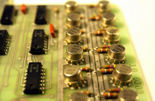
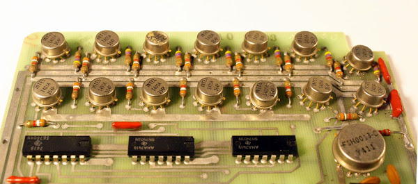
I got a display board from a Datapoint 2200[5], which uses Intel 1405 shift registers for the display storage. This board uses 14 shift registers and holds 896 bytes.[6] Shift-register memory was convenient for a video display board, since the circuitry needed to access each character in sequence to display it.

Intel 1405 shift registers provide memory storage for a Datapoint 2200 display.

Intel 1405 shift registers provide memory storage for a Datapoint 2200 display.

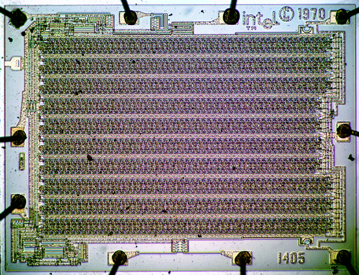
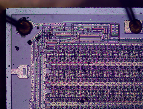
I opened up one of the shift register chips with a hacksaw and looked at it under a metallurgical microscope to get some die photos. Since the shift registers are in metal cans, they are easy to open up, unlike the plastic packages used by most chips. The following photo shows the die. The chip is fairly simple, with most of the chip taken up with the shift register cells. Around the outside of the chip you can see the nine pads with black wires connected.

The die shows some of the reasons that shift registers were cheaper than RAM chips. Unlike a RAM chip, the chip does not need to form a regular grid — the rows in the middle are shorter than the others because of the pin on the right. In addition, the chip doesn't need any address decoding logic. Thus, more bits can be fit onto a chip. Because there are no address lines, the chip has fewer pins than a RAM chip and can fit into a smaller package.

Die shot of the Intel 1405 MOS 512-bit shift register memory.

Die shot of the Intel 1405 MOS 512-bit shift register memory.

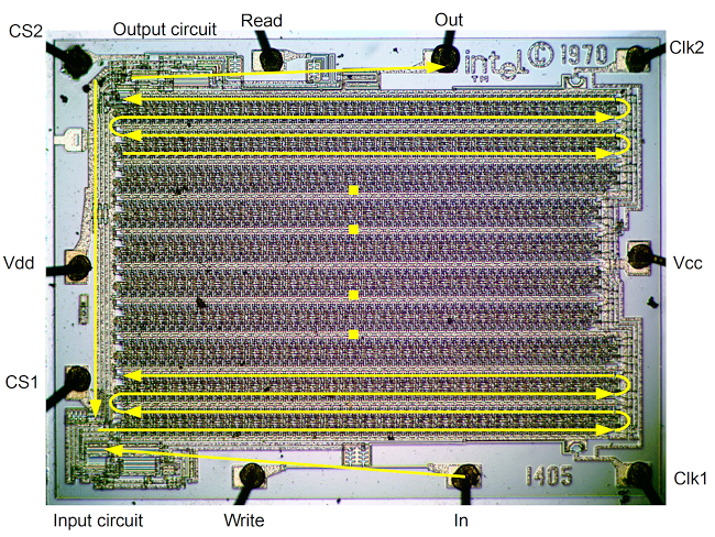
The diagram below shows the flow of bits through the shift register, in yellow. Bits enter through the input pin at the bottom. They zig-zag through the 20 rows of the shift register and exit at the top through the output pin. Bits recirculate back to the input along the left. The clock lines are at the right and are connected to each cell of the shift register.

Labeled die shot of the Intel 1405 MOS 512-bit shift register memory.

Labeled die shot of the Intel 1405 MOS 512-bit shift register memory.

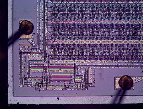
In the lower left is the circuit to control input to the shift register, which consists of a few gates. Either a new bit can be written to the shift register each cycle, or the exiting bit can recirculate and re-enter the shift register. The photo below zooms in on this circuit. The four vertical wires at the left are the chip select 2, chip select 1, recirculated bit, and Vdd.

Input circuit of the 1405 shift register.

Input circuit of the 1405 shift register.

The image below shows the circuit to control the output from the shift register, which is in the upper left of the chip. The chip has two chip select inputs, which makes it convenient to arrange the shift registers in a grid with one set of lines enabling a row and a perpendicular set of lines enabling a column.

Output circuit of the 1405 shift register.

Output circuit of the 1405 shift register.
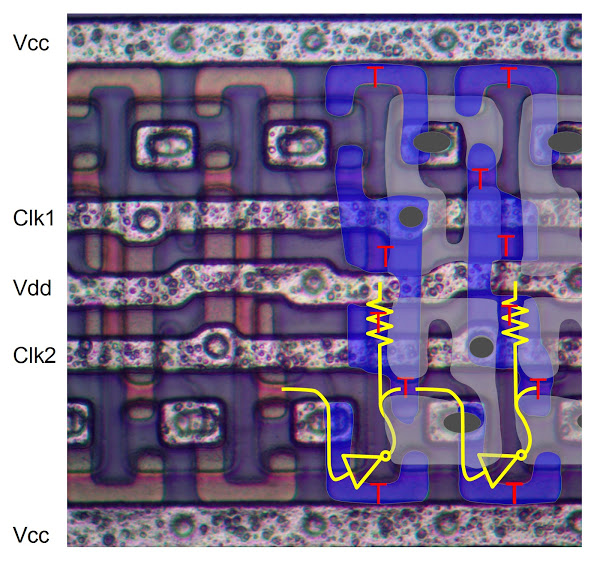
The image below shows the shift register cells at high magnification. On the left is the actual die photo, while the right labels the components of the die. Bits flow to the right through the bottom half of the picture, and then back to the left in the top half.

The large U shapes at the bottom are transistors (red T's) that form inverters (drawn in yellow). Between each inverter is a pass transistor that controls the flow of bits from inverter to inverter. The first T is connected to clock 1, allowing the bit to flow from the first inverter to the second when clock 1 is activated. The next T is connected to clock 2, passing the bit along another step on clock 2. As the clock lines are triggered in sequence, the bits pass step-by-step through the shift register.

The chip uses silicon-gate technology. This was an important innovation in chip design that was developed in 1968 at Fairchild by Federico Faggin (who also developed the Z80), and became a core technology at Intel. With this technology, polysilicon is used as the gates for transistors instead of aluminum metal, as previous MOS integrated circuits used. For various reasons, this made chips much faster and easier to manufacture.

In the picture below, polysilicon is indicated in blue. Where it overlaps the underlying doped silicon, a transistor is formed (red T). The horizontal gray lines are the metal layer, with the voltage supplies and the clocks. The circles show connections between the different layers.[7]

Close up of the cells in an Intel 1405 512-bit shift register memory. The actual photo is on the left, and the circuit is drawn on the right.

Close up of the cells in an Intel 1405 512-bit shift register memory. The actual photo is on the left, and the circuit is drawn on the right.

The clock driver

The display circuit board below has 14 shift registers in round metal cans. But there's a huge metal can at the right — what is this IC? That turns out to be the driver chip that provides the clock signals for the shift registers, and it's pretty interesting inside.

The shift registers require two alternating clock signals to shift. These signals must not overlap, or else the data will get messed up. In addition, the shift registers require up to 30 volts in the clock, due to their old technology. Finally, a lot of current (500mA) is needed in the clock signals to drive all the chips. To meet these requirements, a special clock driver chip is used to generate the clock signals. This is the Fairchild SH0013-C "Two phase MOS clock driver".[8]

1405 shift registers provide 896 bytes of storage on a Datapoint 2200 display card.

1405 shift registers provide 896 bytes of storage on a Datapoint 2200 display card.

I expected to find an IC with big transistors inside the clock driver chip, but opening it up revealed something entirely different. Inside is a hybrid integrated circuit made up of eight separate silicon dies mounted on a tiny circuit board and connected with gold traces and gold wires. In addition, there are thick film resistors printed onto the board — these are the black "E" shapes in the picture below.

Interactive viewer

The image and schematic[8] below are an interactive exploration of the SH0013 clock driver. Click a component to see its location on the board and in the schematic highlighted. The box below will give an explanation of the component.

Click image below for details.

Conclusion

While using shift registers as memory seems bizarre now, it was a cost-effective way to implement storage in 1970. Looking inside the shift register chips shows how they work and how they could be implemented more cheaply than RAM. Providing the high-power clock signals required a special driver chip, which turns out to be a hybrid circuit with tiny semiconductors and resistors on a circuit board in a large metal IC package.

Notes and references

[1] Intel didn't invent the memory chip, of course. There were many companies making memory chips in the 1960s. For instance, Texas Instruments announced the SN5481 bipolar memory chip in 1966 (Electronics, V39 #1, p151) and Transitron had the TMC 3162 and 3164 16-bit RAM (Electrical Design News, Volume 11, p14). In 1968, RCA made 72-bit CMOS memories for the Air Force (document, photo). Lee Boysel built 256-bit dynamic RAMs at Fairchild in 1968 and 1K dynamic RAMs at Four Phase Systems in 1969 (1970 — MOS Dynamic RAM Competes with Magnetic Core Memory on Price and Boysel presentation). For more information on the history of memory technology, see 1966 — Semiconductor RAMs Serve High-speed Storage Needs and History of Semiconductor Engineering, p215. Another source for memory history is To the Digital Age: Research Labs, Start-up Companies, and the Rise of MOS Technology, p193.

[2] Memory chips started out very expensive, but prices rapidly dropped. Computer Design Volume 9 page 28, 1970, announced a price drop of the 3101 from $99.50 to $40 in small volumes. Electrical Design News Volume 15, 1970 gave the initial price of the 1405 as $13.30 in quantities of 100. Ironically, the Intel 3101 is now a collector's item and costs much more than the original price on eBay — hundreds of dollars for the right package.

[3] The datasheet for the 1405A shift register is available at Intel-vintage.info or Intel's data catalog 1976 (at archive.org).

[4] Many companies made shift register memories. For instance, in 1969 Philco (an electronics manufacturer owned by Ford Motor Company) claimed to have the longest commercially available shift register at 256 bits (Electronic Design, Volume 17, p251). For lots more information on shift register memory, see Don Lancaster's December 1974 Radio-Electronics article, " How it works: IC MOS shift registers.

[5] I obtained the Datapoint display board on eBay from Zuigadrummer, who currently has other Datapoint boards for sale. She was very helpful to me and I recommend her.

[6] The Datapoint 2200's display provided 12 lines of 80 characters. The display memory held 1024 7-bit ASCII characters. A pair of shift registers provided 1024 bits of storage, with 7 pairs in total.

[7] For those who want to know more details of the layout... The resistor symbols are not actually resistors, but clocked precharge transistors that pull the inverter outputs high. A few years later, MOS chips would use depletion transistors instead.

The metal rectangles form connections between the silicon layer and the polysilicon layer. This technique was soon obsoleted by buried contacts which connected the two layers directly without using the metal layer. This made chip layout easier, since the metal layer could be used for interconnections without being interrupted by these connections.

The gray blobs show the undoped silicon, which can be considered non-conductive. The doped silicon is conductive, except where the polysilicon crosses it and forms a transistor. Doped and undoped silicon are hard to distinguish in the die photo, but the boundary between them is visible as a faint black line. The polysilicon is much more visible in the die photo; it is orange, or red when it forms a transistor. The colors are due to the thicknesses of the layers.

[8] A datasheet for the SH0013 clock driver is in the 1973 Fairchild Linear Integrated Circuits Data Catalog, page 6-126. A datasheet for the equivalent MH0013 is in the 1972 National MOS Integrated Circuits databook, page 123.

Down to the silicon: how the Z80's registers are implemented

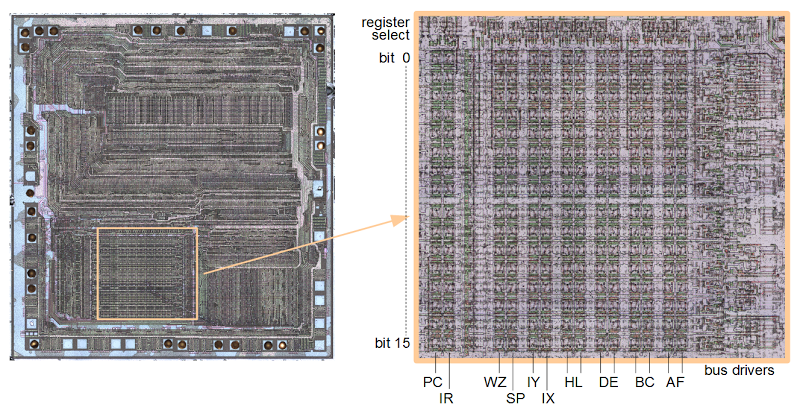
The 8-bit Z80 microprocessor is famed for use in many early personal computers such the Osborne 1, TRS-80, and Sinclair ZX Spectrum. The Z80 has an innovative design for its internal registers, with two sets of general-purpose registers. The diagram below shows a highly-magnified photo of the Z80 chip, from the Visual 6502 team. Zooming in on the register file at the right, the transistors that make up the registers are visible (with difficulty). Each register is in a column, with the low bit on top and high bit on the bottom. This article explains the details of the Z80's register structure: its architecture, how it works, and exactly how it is implemented, based on my reverse-engineering of the chip.

The die of the Z80 microprocessor, zooming in on the register file. Each register is stored vertically, with bit 0 and the top and bit 15 at the bottom. At the right, drivers connect the registers to the data buses. At the top, circuitry selects a register.

The die of the Z80 microprocessor, zooming in on the register file. Each register is stored vertically, with bit 0 and the top and bit 15 at the bottom. There are two sets of AF/BC/DE/HL registers. At the right, drivers connect the registers to the data buses. At the top, circuitry selects a register.

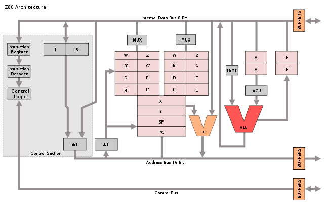
The Z80's architecture is often described with the diagram below, which shows the programmer's model of the chip.[1][2] But as we will see, the Z80's actual register and bus organization differs from this diagram in many ways. For instance, the data bus on the real chip has multiple segments. The diagram shows a separate incrementer for the refresh register (IR), an adder for IX and IY offsets, and a W'Z' register but those don't exist on the real chip. The Z80 shows that the physical implementation of a chip may be very different from how it appears logically.

Programmer's model of Z80 architecture by Appaloosa. Licensed under CC BY-SA 3.0

Programmer's model of Z80 architecture from Wikipedia. Diagram by Appaloosa CC BY-SA 3.0. Original by Rodnay Zaks.

Register overview and layout

The diagram below shows how the Z80's registers are physically arranged on the chip, matching the die photo above. The register file consists of 14 pairs of 8-bit registers. In many cases, a pair of 8-bit registers is treated as a single 16-bit register. The bits are ordered from 0 at the top to 15 at the bottom, so the low-order byte is on the top and the high-order byte is on the bottom.

At the right of the register file are the 8-bit accumulator (A) and 8-bit flag register (F). The accumulator holds the result of arithmetic and logic operations, so it is a very important register. The flag register holds condition flags, for instance indicating a zero value, negative value, overflow value or other conditions.

Note that there are two A registers and two F registers, along with two of BC, DE, and HL. The Z80 is described as having a main register set (AF, BC, DE, and HL) and an alternate register set (A'F', B'C', D'E', and H'L'), and this is how the architecture diagram earlier is drawn. It turns out, though, that this is not how the Z80 is actually implemented. There isn't a main register set and an alternate register set. Instead, there are two of each register and either one can be the main or alternate. This will be explained in more detail below.

Structure of the Z-80's register file. The address is 16 bits wide, while the data buses are 8 bits wide. Gray lines show switches between bus segments.

Structure of the Z-80's register file as implemented on the chip. The address is 16 bits wide, while the data buses are 8 bits wide. Gray lines show switches between bus segments.

To the left of the AF registers are the two general-purpose BC registers. These can be used as 8-bit registers (B or C), or a 16-bit register (BC). Next to them are the similar DE and HL registers. The HL register is often used to reference a location in memory; H holds the high byte of the address, and L holds the low byte. This register structure is based on the earlier 8080 microprocessor. (As will be explained later, DE and HL can swap roles, so these registers should really be labeled H/D and L/E.)

Next to the left are the 16-bit IX and IY index registers. These are used to point to the start of a region in memory, such as a table of data. The 16-bit stack pointer SP is to the left of the index registers. The stack pointer indicates the top of the stack in memory. Data is pushed and popped from the stack, for instance in subroutine calls. To the left of the stack pointer are the 8-bit W and Z registers. As will be discussed below, these are internal registers used for temporary storage and are invisible to the programmer.

Separated from the previous registers is the special-purpose memory refresh register R, which simplifies the hardware when dynamic memory is used.[3] The interrupt page address register I is below R, and is used for interrupt handling. (It provides the high-order byte of an interrupt handler address.)

Finally, at the left is the 16-bit PC (Program Counter), which steps through memory to fetch instructions. Since it is 16 bits, the Z80 can address 64K of memory. Its position next to the incrementer/decrementer is important and will be discussed below.

The Z80's register buses

An important part of the Z80's architecture is how the registers are connected to other parts of the system by various buses. The Z80 is described as having a 16-bit address bus and an 8-bit data bus, but the implementation is more complicated.[3][4] The point of this complexity is to permit multiple register activities as the same time, so the chip can execute faster.

The PC and IR registers are separated from the rest of the registers. As the diagram above shows, these registers are connected to the other registers through a 16-bit bus (thick black line). However, this bus can be connected or disconnected as needed (by pass transistors indicated by the vertical gray line). When disconnected, the PC and R registers can be updated while registers on the right are in use.

The internal register bus connects the PC and IR registers to an incrementer/decrementer/latch circuit. It has multiple uses, but the main purpose is to step the PC from one instruction to the next, and to increment the R register to refresh memory. The resulting address goes to the address pins via the address bus (magenta). I describe the incrementer/decrementer/latch in detail here.

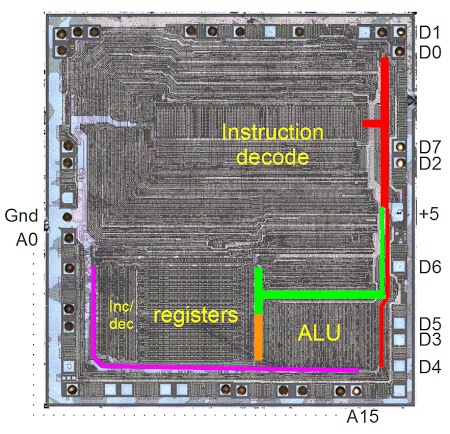
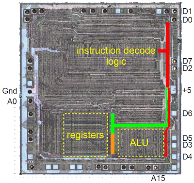
At the right, separate 8-bit data buses connect to the low-order and high-order registers. These two buses can be connected or disconnected as needed. The lower bus (orange) provides access to the ALU (arithmetic logic unit). The upper bus (green) connects to another data bus (red) that accesses the data pins and instruction decoder.

Photo of the Z80 die. The address bus is indicated in purple. The data bus segments are in red, green, and orange.

Photo of the Z80 die. The address bus is indicated in purple. The data bus segments are in red, green, and orange.

Specifying registers in the opcodes

The Z80 uses 8-bit opcodes to specify its instructions, and these instructions are carefully designed to efficiently specify which registers to use. Register instructions normally use three bits to specify the register used: 000=B, 001=C, 010=D, 011=E, 100=H, 101=L, 110=indirect through HL, 111=A.[5] For instance, the ADD instructions have the 8-bit binary values 10000rrr, where the rrr bits specify the register to use as above. Note that in this pattern the two high-order bits specify the register pair, while the low order bit specifies which half of the pair to use; for example 00x is BC, 000 is B, and 001 is C. For instructions operating on a register pair (such as 16-bit increment INC), the opcode uses just the two bits to specify the pair.

By using this structure for opcodes, the instruction decoding logic is simplified since the same circuitry can be reused to select a register or register pair for many different instructions. Instruction decode circuitry located above the register file uses the two bits to select the register pair and then uses the third bit to pick the lower or upper half of the register file.

The register selection bits can be in bits 2-0 of the instruction, for example AND; in bits 5-3 of the instruction, for example DEC (decrement); or in both positions, for example register-to-register LD.[6] To handle this, a multiplexer selects the appropriate group of bits and feeds them into the register select logic. Thus, the same circuit efficiently handles register bits in either position. By designing the instruction set in this way, the Z80 combines the ability to use a large register set with a compact hardware implementation.

Swapping registers through register renaming

The Z80 has several instructions to swap registers or register sets. The EX DE, HL instruction exchanges the DE and HL registers. The EX AF, AF' instruction exchanges the AF and AF' registers. The EXX instruction exchanges the BC, DE, and HL registers with the BC', DE', and HL' registers. These instructions complete very quickly, which raises the question of how multiple 16-bit register values can move around the chip at once.

It turns out that these instructions don't move anything. They just toggle a bit that renames the appropriate registers. For example, consider exchanging the DE and HL registers. If the DE/HL bit is set, an instruction acting on DE uses the first register and an instruction acting on HL uses the second register. If the bit is cleared, a DE instruction uses the second register and a HL instruction uses the first register. Thus, from the programmer's perspective, it looks like the values in the registers have been swapped, but in fact just the meanings/names/labels of the registers have been swapped. Likewise, a bit selects between AF and AF', and a bit selects between BC, DE, HL and the alternates. In all, there are four registers that can be used for DE or HL; physically there aren't separate DE and HL registers.

The hardware to implement register renaming is interesting, using four toggle flip flops.[7] These flip flops are toggled by the appropriate EX and EXX instructions. One flip flop handles AF/AF'. The second flip flop handles BC/DE/HL vs BC'/DE'/HL'. The last two flip flops handle DE vs HL and DE' vs HL'. Note that two flip flops are required since DE and HL can be swapped independently in either register bank.

The flags

The flags have a dual existence. The flags are stored inside the register file, but at the start of every instruction,[8] they are copied into latches above the ALU. From this location, the flags can be used and modified by the ALU. (For example, add or shift operations use the carry flag.) At the end of an instruction that affects flags, the flags are copied from the latches back to the register file.

Most of the flags are generated by the ALU (details here). The circuitry to set and use the carry is complicated, since it is used in different ways by shifts and rotates, as well as arithmetic. Conditional operations are another important use of the flags.[9]

The WZ temporary registers

The Z80 (like the 8080 and 8085) has a WZ register pair that is used for temporary storage but is invisible to the programmer. The primary use of WZ is to hold an operand from a two or three byte instruction until it can be used.[10]

The JP (jump) instruction shows why the WZ registers are necessary. This instruction reads a two-byte address following the opcode and jumps to that address. Since the Z80 only reads one byte at a time, the address bytes must be stored somewhere while being read in, before the jump takes place. (If you read the bytes directly into the program counter, you'd end up jumping to a half-old half-new address.) The WZ register pair is used to hold the target address as it gets read in. The CALL (subroutine call) instruction is similar.

Another example is EX (SP), HL which exchanges two bytes on the stack with the HL register. The WZ register pair holds the values at (SP+1) and (SP) temporarily during the exchange.

How the registers are implemented in silicon

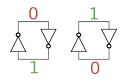
The building block for the registers is a simple circuit to store one bit, consisting of two inverters in a feedback loop. In the diagram below, if the top wire has a 0, the right inverter will output a 1 to the bottom wire. The left inverter will then output a 0 to the top wire, completing the cycle. Thus, the circuit is stable and will "remember" the 0. Likewise, if the top wire is a 1, this will get inverted to a 0 at the bottom wire, and back to a 1 at the top. Thus, this circuit can store either a 0 or a 1, forming a 1-bit memory.[11]

In the Z80, two coupled inverters hold a single bit in the register. This circuit is stable in either the 0 or 1 state.

In the Z80, two coupled inverters hold a single bit in the register. This circuit is stable in either the 0 or 1 state.

How does a value get stored into this inverter pair? Surprisingly, the Z80 just puts stronger signals on the wires, forcing the inverters to take the new values.[12] There's no logic involved, just "might makes right". (In contrast, the 6502 uses an additional transistor in the inverter feedback loop to break the feedback loop when writing a new value.)

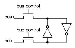
To support multiple registers, each register bit is connected to bus lines by two pass transistors. These transistors act as switches that turn on to connect one register to the bus. Each register has a separate bus control signal, connecting the register to the bus when needed. Note that there are two bus lines for each bit - the value and its complement. As explained above, to write a new value to the bit, the new value is forced into the inverters. There are 16 pairs of bus lines running horizontally through the register file, one for each bit.

Each bit of register storage is connected to the bus by pass transistors, allowing the bit to be read or written.

Each bit of register storage is connected to the bus by pass transistors, allowing the bit to be read or written.

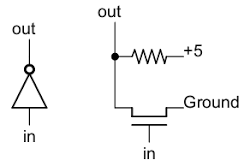
Next, to see how an inverter works, the schematic below shows how an inverter is implemented in the Z80. The Z80 uses NMOS transistors, which can be viewed as simple switches. If a 1 is input to the transistor's gate, the switch closes, connecting ground (0) to the output. If a 0 is input to the gate, the switch opens and the output is pulled high (1) by the resistor. Thus, the output is the opposite of the input.[13]

Implementation of an inverter in NMOS.

Implementation of an inverter in NMOS.

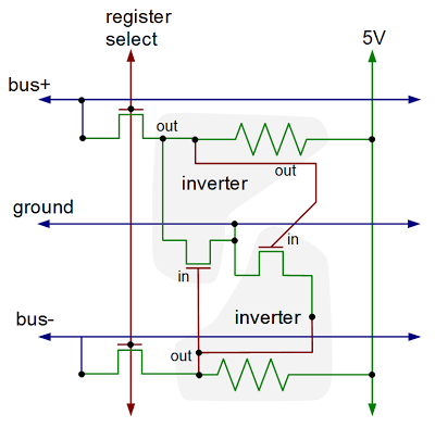
Putting this all together - the two inverters and the pass transistors - yields the following schematic for a single bit in the register file. The layout of the schematic matches the actual silicon where the inverters are positioned to minimize the space they take up. The bus lines and ground run horizontally. The control line to connect a register to the buses runs vertically, along with the 5V power line.

Schematic of one bit inside the Z80's register file.

Schematic of one bit inside the Z80's register file.

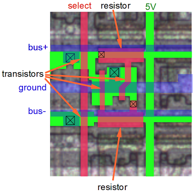
The diagram below shows the physical implementation of a register bit in the Z80, superimposed on a photo of the die. It's tricky to understand this, but comparing with the schematic above should help. The silicon is in green, the polysilicon is in red, and the metal lines are in blue. Transistors occur where the polysilicon (red) crosses the silicon (green). The X in a box indicates a contact connecting two layers. Note the large area taken up by the resistors (which are formed from depletion-mode transistors). Additional register bits can be seen in the photo, surrounding the bit illustrated.

This diagram shows the layout on silicon of one bit of register storage. Green indicates silicon, red indicates polysilicon, and blue is the metal layer.

This diagram shows the layout on silicon of one bit of register storage. Green indicates silicon, red indicates polysilicon, and blue is the metal layer.

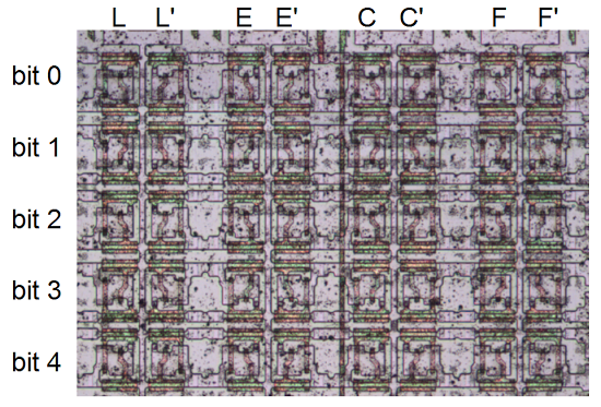
Zooming out, the picture below shows the upper right part of the register file. Each bit consists of a structure like the one above. Each column is a separate register, with a separate control line, and each row is one of the bits. The columns are in groups of two, with the register control lines between the pairs of columns. Zooming out more, the image at the top of the article shows the full register file and its location in the chip. Thus, you can see how the entire register file is built up from simple transistors.

A detail of the Z80 chip, showing part of the register file.

A detail of the Z80 chip, showing part of the register file.

Comparison with the 6502 and 8085

While the Z80's register complement is tiny compared to current processors, it has a solid register set by 1976 standards - about twice as many registers as the 8085 and about four times as many registers as the 6502. Because they share the 8080 heritage, many of the 8085's registers are similar to the Z80, but the Z80 adds the IX and IY index registers, as well as the second set of registers.

The physical structure of the Z80's register file is similar to the 8085 register file. Both use 6-transistor static latches arranged into a 16-bit wide grid. The 8085, however, uses complex differential sense amplifiers to read the values from the registers. The Z80, by contrast, just uses regular gates. I suspect the 8085's designers saved space by making the register transistors as small as possible, requiring extra circuitry to read the weak values on the bus lines.

The 6502, on the other hand, doesn't have a separate register file. Instead, registers are put on the chip where it turns out to be convenient. Since the 6502 has fewer registers, the register circuitry doesn't need to be as optimized and each bit is more complex. The 6502 adds a transistor to each bit so it is clocked, and separate pass transistors for read and write. One consequence is direct register-to-register transfers are possible on the 6502, since the source and destination registers can be distinguished. Instead of a separate incrementer unit, the 6502's program counter is tangled in with the incrementer circuitry.

Conclusion

By looking at the silicon of the Z80 in detail, we can determine exactly how it works. The Z80's register file has more complexity than you'd expect and the hardware implementation is different from published architecture diagrams. By splitting the register file in two, the Z80 runs faster since registers can be updated in parallel. The Z80 includes a WZ register pair for temporary storage that isn't visible to the programmer. The Z80's register storage has many similarities to the 8085, both in the registers provided and their hardware implementation, but is very different from the 6502.

Credits: This couldn't have been done without the Visual 6502 team especially Chris Smith, Ed Spittles, Pavel Zima, Phil Mainwaring, and Julien Oster. All die photos are from the visual 6502 team.

Notes and references

[1] There are many variants of that architecture diagram; the one above is from Wikipedia. The original source of the common Z80 architecture diagram is the book Programming the Z80 by Rodnay Zaks, page 65 (HTML or PDF). The book is an extremely detailed guide to the Z80, down to the instruction cycles. I don't mean to criticize the architecture diagram by pointing out differences between it and the actual silicon. After all, it is a logic-level diagram intended for use by programmers, not a hardware reference. But it is interesting to see the differences between the programmer's view and the hardware implementation.

[2] Zilog's Z80 CPU user manual is a key reference on the instruction set and operation of the Z80, but it doesn't provide any information on the internal architecture.

[3] The Z80's memory refresh feature is described in patent 4332008. Figure 15 in the patent shows the segmented data bus used by the Z80, although it is a mirror image of the actual die.

[4] I wrote more about the data buses in the Z-80 in Why the Z-80's data pins are scrambled.

[5] The bit pattern 110 is an exception to the encoding of registers in instructions, since it refers to a memory location indexed by the HL register pair, rather than a register. Likewise the bit pattern 11x referring to a register pair is also an exception. It can indicate the SP register, for example in 16-bit LD, INC and DEC instructions.

[6] The Z80 specifies registers in instruction bits 0-2 and bits 3-5. This maps cleanly onto octal, but not hexadecimal. One consequence is the opcodes are more logical if you arrange them in octal (like this), instead of hexadecimal (like this). Perhaps the designers of the Z80 were thinking in octal and not hex.

[7] The toggle flip flops are unlike standard flip flops formed from gates. Instead they use pass transistors; this lets it hold the previous state while toggling to avoid oscillation. Because the pass transistor circuits depend on capacitance holding the values, you have to keep the clock running. This is one reason the clock in the Z80 can't stop for more than a couple microseconds. (The CMOS version is different and the clock can stop arbitrarily long.) From looking at the silicon, it appears that these flip flops required some modifications to work reliably, probably to ensure they toggled exactly once.

These flip flops have no reset logic, so it is unpredictable how the registers get assigned on power-up. Since there's no way to tell which register is which, this doesn't matter.

The active DE vs HL flip flop swaps the DE and HL register control lines using pass-gate multiplexers. The main vs alternate register set flip flops direct each AF/BC/DE/HL register control line to one of the two registers in the pair.

[8] Like many processors of its era, the Z80 starts fetching a new instruction before the previous instruction is finished; this is known as fetch/execute overlap. As a result, the flags are actually written from the latches to the register file three cycles into the next instruction (i.e. T3), and the flags are read from the register file into the latches four cycles into the instruction (i.e. T4).

[9] I'll explain briefly how conditional instructions such as jump (JP) work with the flags. Bits 4 and 5 of the opcode select the flag to use (via a multiplexer just to the right of the registers). Bit 3 of the opcode indicates the desired value (clear or set); this bit is XORed with the selected flag's value. The result indicates if the desired condition is satisfied or not, and is fed into the control logic to determine the appropriate action. The JR and DJNZ don't exactly fit the pattern so a couple additional gates adjust their bits to pick the right flags.

[10] For more explanation of the WZ registers, see Programming the Z80, pages 87-91.

[11] The register storage in the Z80 is called "static" memory, since it will store data as long as the circuit has power. In contrast, your computer uses dynamic memory, which will lose data in milliseconds if the data isn't constantly refreshed. The advantage of dynamic memory is it is much simpler (a transistor and a capacitor), and thus each cell is much smaller. (This is how DRAM can fit gigabits onto a single chip.) Another alternative is flash memory, which has the big advantage of keeping its contents while the power is turned off.

[12] If you've built electronic circuits, it may seem dodgy to force the inverters to change values by overpowering the outputs. But this is a standard technique in chips. To understand what happens, remember that in an NMOS circuit, a 0 output is created by a transistor to ground, while a 1 output is made by a much weaker resistor. So if one of the inverters is outputting a 1 and a 0 is connected to the output, the 0 will "win". This will cause the other inverter to immediately switch to 1. At this point, the original inverter will switch to output 0 and the inverter pair is now stable with the new values.

To improve speed, and to prevent a low voltage on the bus from accidentally clearing a bit while reading a register, the bus lines are all precharged to +5 every clock cycle. A low output from an inverter will have no trouble pulling the bus line low, and a high output will leave the bus line high. The precharging is done through transistors in the space between the IR and WZ registers.

[13] One disadvantage of NMOS logic is the pull-up resistors waste power. In addition, the output is fairly slow (by computer standards) to change from 0 to 1 because of the limited current through the resistor. For these, reasons, NMOS has been almost entirely replaced by CMOS logic which instead of resistors uses complementary transistors to pull the output high. (As a result, CMOS uses almost no power except while switching outputs from one state to another. For this reason, CMOS power usage scales up with frequency, which is why CPUs are hitting clock limits - they're too hot to run any faster.)

Mining Bitcoin with pencil and paper: 0.67 hashes per day

I decided to see how practical it would be to mine Bitcoin with pencil and paper. It turns out that the SHA-256 algorithm used for mining is pretty simple and can in fact be done by hand. Not surprisingly, the process is extremely slow compared to hardware mining and is entirely impractical. But performing the algorithm manually is a good way to understand exactly how it works.

A pencil-and-paper round of SHA-256

A pencil-and-paper round of SHA-256

The mining process

Bitcoin mining is a key part of the security of the Bitcoin system. The idea is that Bitcoin miners group a bunch of Bitcoin transactions into a block, then repeatedly perform a cryptographic operation called hashing zillions of times until someone finds a special extremely rare hash value. At this point, the block has been mined and becomes part of the Bitcoin block chain. The hashing task itself doesn't accomplish anything useful in itself, but because finding a successful block is so difficult, it ensures that no individual has the resources to take over the Bitcoin system. For more details on mining, see my Bitcoin mining article.

A cryptographic hash function takes a block of input data and creates a smaller, unpredictable output. The hash function is designed so there's no "short cut" to get the desired output - you just have to keep hashing blocks until you find one by brute force that works. For Bitcoin, the hash function is a function called SHA-256. To provide additional security, Bitcoin applies the SHA-256 function twice, a process known as double-SHA-256.

In Bitcoin, a successful hash is one that starts with enough zeros.[1] Just as it is rare to find a phone number or license plate ending in multiple zeros, it is rare to find a hash starting with multiple zeros. But Bitcoin is exponentially harder. Currently, a successful hash must start with approximately 17 zeros, so only one out of 1.4x10²⁰ hashes will be successful. In other words, finding a successful hash is harder than finding a particular grain of sand out of all the grains of sand on Earth.

The following diagram shows a block in the Bitcoin blockchain along with its hash. The yellow bytes are hashed to generate the block hash. In this case, the resulting hash starts with enough zeros so mining was successful. However, the hash will almost always be unsuccessful. In that case, the miner changes the nonce value or other block contents and tries again.

Structure of a Bitcoin block

Structure of a Bitcoin block

The SHA-256 hash algorithm used by Bitcoin

The SHA-256 hash algorithm takes input blocks of 512 bits (i.e. 64 bytes), combines the data cryptographically, and generates a 256-bit (32 byte) output. The SHA-256 algorithm consists of a relatively simple round repeated 64 times. The diagram below shows one round, which takes eight 4-byte inputs, A through H, performs a few operations, and generates new values of A through H.

SHA-256 round, from Wikipedia

One round of the SHA-256 algorithm showing the 8 input blocks A-H, the processing steps, and the new blocks. Diagram created by kockmeyer, CC BY-SA 3.0.

The blue boxes mix up the values in non-linear ways that are hard to analyze cryptographically. Since the algorithm uses several different functions, discovering an attack is harder. (If you could figure out a mathematical shortcut to generate successful hashes, you could take over Bitcoin mining.)

The Ma majority box looks at the bits of A, B, and C. For each position, if the majority of the bits are 0, it outputs 0. Otherwise it outputs 1. That is, for each position in A, B, and C, look at the number of 1 bits. If it is zero or one, output 0. If it is two or three, output 1.

The Σ0 box rotates the bits of A to form three rotated versions, and then sums them together modulo 2. In other words, if the number of 1 bits is odd, the sum is 1; otherwise, it is 0. The three values in the sum are A rotated right by 2 bits, 13 bits, and 22 bits.

The Ch "choose" box chooses output bits based on the value of input E. If a bit of E is 1, the output bit is the corresponding bit of F. If a bit of E is 0, the output bit is the corresponding bit of G. In this way, the bits of F and G are shuffled together based on the value of E.

The next box Σ1 rotates and sums the bits of E, similar to Σ0 except the shifts are 6, 11, and 25 bits.

The red boxes perform 32-bit addition, generating new values for A and E. The input Wt is based on the input data, slightly processed. (This is where the input block gets fed into the algorithm.) The input Kt is a constant defined for each round.[2]

As can be seen from the diagram above, only A and E are changed in a round. The other values pass through unchanged, with the old A value becoming the new B value, the old B value becoming the new C value and so forth. Although each round of SHA-256 doesn't change the data much, after 64 rounds the input data will be completely scrambled.[3]

Manual mining

The video below shows how the SHA-256 hashing steps described above can be performed with pencil and paper. I perform the first round of hashing to mine a block. Completing this round took me 16 minutes, 45 seconds.

To explain what's on the paper: I've written each block A through H in hex on a separate row and put the binary value below. The maj operation appears below C, and the shifts and Σ0 appear above row A. Likewise, the choose operation appears below G, and the shifts and Σ1 above E. In the lower right, a bunch of terms are added together, corresponding to the first three red sum boxes. In the upper right, this sum is used to generate the new A value, and in the middle right, this sum is used to generate the new E value. These steps all correspond to the diagram and discussion above.

I also manually performed another hash round, the last round to finish hashing the Bitcoin block. In the image below, the hash result is highlighted in yellow. The zeroes in this hash show that it is a successful hash. Note that the zeroes are at the end of the hash. The reason is that Bitcoin inconveniently reverses all the bytes generated by SHA-256.[4]

Last pencil-and-paper round of SHA-256, showing a successfully-mined Bitcoin block.

Last pencil-and-paper round of SHA-256, showing a successfully-mined Bitcoin block.

What this means for mining hardware

Each step of SHA-256 is very easy to implement in digital logic - simple Boolean operations and 32-bit addition. (If you've studied electronics, you can probably visualize the circuits already.) For this reason, custom ASIC chips can implement the SHA-256 algorithm very efficiently in hardware, putting hundreds of rounds on a chip in parallel. The image below shows a mining chip that runs at 2-3 billion hashes/second; Zeptobars has more photos.

The silicon die inside a Bitfury ASIC chip. This chip mines Bitcoin at 2-3 Ghash/second. Image from http://zeptobars.ru/en/read/bitfury-bitcoin-mining-chip (CC BY 3.0 license)

The silicon die inside a Bitfury ASIC chip. This chip mines Bitcoin at 2-3 Ghash/second. Image from Zeptobars. (CC BY 3.0)

In contrast, Litecoin, Dogecoin, and similar altcoins use the scrypt hash algorithm, which is intentionally designed to be difficult to implement in hardware. It stores 1024 different hash values into memory, and then combines them in unpredictable ways to get the final result. As a result, much more circuitry and memory is required for scrypt than for SHA-256 hashes. You can see the impact by looking at mining hardware, which is thousands of times slower for scrypt (Litecoin, etc) than for SHA-256 (Bitcoin).

Conclusion

The SHA-256 algorithm is surprisingly simple, easy enough to do by hand. (The elliptic curve algorithm for signing Bitcoin transactions would be very painful to do by hand since it has lots of multiplication of 32-byte integers.) Doing one round of SHA-256 by hand took me 16 minutes, 45 seconds. At this rate, hashing a full Bitcoin block (128 rounds)[3] would take 1.49 days, for a hash rate of 0.67 hashes per day (although I would probably get faster with practice). In comparison, current Bitcoin mining hardware does several terahashes per second, about a quintillion times faster than my manual hashing. Needless to say, manual Bitcoin mining is not at all practical.[5]

A Reddit reader asked about my energy consumption. There's not much physical exertion, so assuming a resting metabolic rate of 1500kcal/day, manual hashing works out to almost 10 megajoules/hash. A typical energy consumption for mining hardware is 1000 megahashes/joule. So I'm less energy efficient by a factor of 10^16, or 10 quadrillion. The next question is the energy cost. A cheap source of food energy is donuts at $0.23 for 200 kcalories. Electricity here is $0.15/kilowatt-hour, which is cheaper by a factor of 6.7 - closer than I expected. Thus my energy cost per hash is about 67 quadrillion times that of mining hardware. It's clear I'm not going to make my fortune off manual mining, and I haven't even included the cost of all the paper and pencils I'll need.

2017 edit: My Bitcoin mining on paper system is part of the book The Objects That Power the Global Economy, so take a look.

Follow me on Twitter to find out about my latest blog posts.

Notes

[1] It's not exactly the number of zeros at the start of the hash that matters. To be precise, the hash must be less than a particular value that depends on the current Bitcoin difficulty level.

[2] The source of the constants used in SHA-256 is interesting. The NSA designed the SHA-256 algorithm and picked the values for these constants, so how do you know they didn't pick special values that let them break the hash? To avoid suspicion, the initial hash values come from the square roots of the first 8 primes, and the Kt values come from the cube roots of the first 64 primes. Since these constants come from a simple formula, you can trust that the NSA didn't do anything shady (at least with the constants).

[3] Unfortunately the SHA-256 hash works on a block of 512 bits, but the Bitcoin block header is more than 512 bits. Thus, a second set of 64 SHA-256 hash rounds is required on the second half of the Bitcoin block. Next, Bitcoin uses double-SHA-256, so a second application of SHA-256 (64 rounds) is done to the result. Adding this up, hashing an arbitrary Bitcoin block takes 192 rounds in total. However there is a shortcut. Mining involves hashing the same block over and over, just changing the nonce which appears in the second half of the block. Thus, mining can reuse the result of hashing the first 512 bits, and hashing a Bitcoin block typically only requires 128 rounds.

[4] Obviously I didn't just have incredible good fortune to end up with a successful hash. I started the hashing process with a block that had already been successfully mined. In particular I used the one displayed earlier in this article, #286819.

[5] Another problem with manual mining is new blocks are mined about every 10 minutes, so even if I did succeed in mining a block, it would be totally obsolete (orphaned) by the time I finished.

Why the Z-80's data pins are scrambled

If you look closely at the datasheet for a Z-80 chip, you'll notice the data pins are in a random-looking order. The address pins (A) are nicely arranged in order counterclockwise from 0 to 15, but the data pins (D) are all shuffled around.[1] After studying the internals of the chip, I have a hypothesis to explain this.

Pinout of the Z-80, from the Zilog Data Book.

Pinout of the Z-80, from the Zilog Data Book.

I have been reverse-engineering the Z-80 processor using images and data from the Visual 6502 team. The image below is a photograph of the Z-80 die. Around the outside of the chip are the pads that connect to the external pins. (The die photo is rotated 180° compared to the datasheet pinout, if you try to match up the pins.) At the right are the 8 data pins for the Z-80's 8-bit data bus in a strange order.

The 8-bit data bus in the Z-80 is used for communication among the different parts of the chip. But instead of a single data bus, the Z-80 has a complex data bus that is split into 3 segments. The first segment of the data bus (in red) connects to the data pins to the instruction decode logic. The first segment is also connected to the second segment (green). The green data bus provides access to the lower byte of registers and is also connected to the fourth segment of the data bus (orange). The orange data bus is connected to the high byte of registers and also to the ALU (Arithmetic Logic Unit)[2]. Note that because the green segment splits off from the red segment, only half of the red bus (4 bits) goes down to the lower part of the chip. [There was an extra segment in an earlier version of this article.]

The Z-80's silicon die, showing the data and address pins, data buses and other internal components.

The Z-80's silicon die, showing the data and address pins, data buses and other internal components.

The motivation behind splitting the data bus is to allow the chip to perform activities in parallel. For instance an instruction can be read from the data pins into the instruction logic at the same time that data is being copied between the ALU and registers. The partitioned data bus is described briefly in the Z-80 oral history[3], but doesn't appear in architecture diagrams.

The complex structure of the data buses is closely connected to the ordering of the data pins. But before explaining the data pin layout, a few more features of the Z-80 need to be discussed.

How the Z-80 processes instructions

To execute an instruction, the Z-80 loads the instruction from memory through the data pins and feeds it into the instruction decode logic via the red segment of the data bus. First, the instruction is stored from the data bus into the instruction register, which is a simple latch that holds the instruction while it is being executed. This feeds the instruction into the PLA (Programmable Logic Array), which decodes the instruction into approximately 98 different categories (details). The instruction logic below the PLA combines these signals with timing signals and determines exactly what should happen at what step. This logic generates the control signals that control the operation of the register file, ALU, and other parts of the chip.

Since the Z-80 is an 8-bit processor, instruction op codes are 8 bits long. Many of the instructions have the bits arranged as follows:

ggiiirrr

In that arrangement, the two gg bits select a group of instructions (e.g. load or arithmetic), the next three iii bits select the particular instruction, and the last three rrr bits select the register to use. There are many exceptions to this format, but it provides an underlying structure. (This instruction structure was inherited from the 8080 microprocessor, since the Z-80 was designed to be backwards compatible with it.)

Bit instructions in the Z-80

One feature the Z-80 has that goes beyond the 8080 is instructions to set, clear, or test a single bit in a register.[4] These instructions fit the pattern described above, with the top two bits in the instruction selecting the test, clear, or set function, the next three bits in the instruction selecting which bit in the byte to operate on, and the final three bits selecting the register. That is, bits 5, 4, and 3 of the instruction select which of the eight bits in the register to operate on.

The processing of the Z-80's bit operations is unusual compared to other instructions. While most of the instruction execution is controlled by the same instruction decoding logic described above, the bit selection is done by feeding the three instruction bits directly into the ALU, bypassing the instruction decoding logic entirely. That is, there are simple circuits (at the right side of the ALU) to select one of the 8 bits, depending on the instruction that was read in. In the diagram of the chip, you can see the connection between the data bus (red) and the ALU to accomplish this.

The hardware to do the bit selection is fairly straightforward. There are eight 3-input NOR gates, each looking at a different combination of the instruction bits, either inverted or non-inverted. For example, an instruction that operates on bit 2 will have an opcode of the form gg010rrr (since 010 is binary 2). Instruction bit 5 is 0, instruction bit 4 is 1, and instruction bit 3 is 0. (Don't confuse the bits in the instruction with the bit being selected.) In logic, this becomes:

modify_data_bit_2 = (NOT bit5) AND bit4 AND (NOT bit3).

It turns out that NOR gates are easiest to build in silicon (as will be explained below), so the logic in hardware is the equivalent:

modify_data_bit_2 = bit5 NOR (NOT bit4) NOR bit3.

Selection of the other 7 bits is done with similar functions of the instruction bits bit5, bit4, and bit3.

The hardware implementation of bit instructions

For a bit operation, one of the 8 bits will be selected and fed into the ALU. The ALU will then test, clear, or set that bit in the appropriate register. Below is a zoomed-in look at the portion of the die that selects bit 2. This is in the lower right corner of the chip, to the right of the ALU by the D3 pad. The white vertical stripes are metal lines, providing the data lines, control lines, and power and ground. Underneath the metal is the polysilicon layer. Underneath this is silicon layer, where the transistors are. It's hard to make out the polysilicon and silicon structures in this photo, but at the left you can see the horizontal polysilicon bus lines for ALU bits 5 and 2. These lines provide data flow through the ALU, and are how the selected bit is fed into the ALU.

The circuitry in the Z-80 to handle bit operations on bit 2.

The circuitry in the Z-80 to handle bit operations on bit 2.

The data bus provides bits 5, 4, and 3 to this part of the chip. (Just to make thing confusing, the data on the Z-80's data bus is inverted, which is indicated by a slash.) Underneath this bus is the NOR gate (outlined in blue) that computes the function described earlier: bit5 NOR (NOT bit4) NOR bit3. The inverter to bit3 from the inverted bit3 on the data bus is also visible (outlined in yellow). A buffer (green) strengthens this signal. The "ALU load bit value" control line is activated by the instruction decode logic; this control line allows the selected bit to pass into the ALU only for a bit operation.

A NOR gate is a simple circuit when implemented with MOS transistors, as the schematic below shows. The transistors can be thought of as switches that close if their gate (middle connection) receives a 1 input. In the circuit below, if any of the inputs are 1, the corresponding transistor will connect the output to ground, and the output will be 0. Otherwise, the resistor (which is actually a special depletion-mode transistor) will pull the output high and the output is 1. Thus, the output is the NOR of the three inputs.

Schematic of a 3-input NOR gate in the Z-80.

Schematic of a 3-input NOR gate in the Z-80.

The diagram below shows how the above NOR gate is actually implemented in silicon. The diagram is a zoomed-in version of the image above, focusing on the NOR gate (blue outline). Instead of a photograph, the diagram shows the different layers in the chip as extracted by the Visual 6502 team: blue is metal, brown is polysilicon, green is silicon, and orange is a connection between layers. A transistor is formed when polysilicon crosses silicon.

Implementation of a 3-input NOR gate in the Z-80 chip.

Implementation of a 3-input NOR gate in the Z-80 chip.

The "T" symbols indicate the three transistors that are connected to ground (as shown by yellow arrows). The transistors are all connected together in the middle, and the final yellow arrow shows the connection to the output. Finally, the pull-up resistor is at the lower left. The cyan outline matches the outline in the die photo and with difficulty you can find the structures in the photo.

The important thing to notice in the diagram above is that everything is packed together as tightly as possible to get the Z-80 to fit on the available silicon. The layout of the Z-80 was done by hand, with each transistor and connection manually positioned. Every possible trick was used to minimize space - for example, each transistor above is oriented in a different direction. Drafting this layout was an extremely time-consuming task that took Zilog founder Federico Faggin 3 1/2 months of 80-hour weeks[3]. (Yes, the CEO drafted the chip himself!) But you can see from the result that there is very little wasted space in the chip.

The data pins

This article has looked at many different aspects of the Z-80 design, and now it's time to see how they constrain the position of the data pins. First, because the Z-80 splits the data bus into multiple segments, only four data lines run to the lower right corner of the chip. And because the Z-80 was very tight for space, running additional lines would be undesirable. Next, the BIT instructions use instruction bits 3, 4, and 5 to select a particular bit. This was motivated by the instruction structure the Z-80 inherited from the 8080. Finally, the Z-80's ALU requires direct access to instruction bits 3, 4, and 5 to select the particular data bit. Putting these factors together, data pins 3, 4, and 5 are constrained to be in the lower right corner of the chip next to the ALU. This forces the data pins to be out of sequence, and that's why the Z-80 has out-of-order data pins.[5]

Credits: The chip analysis couldn't have been done without the Visual 6502 team especially Chris Smith, Ed Spittles, Pavel Zima, Phil Mainwaring, and Julien Oster.

Notes and references

[1] Even though the Z-80 has out-of-order data pins, it is an improvement over the 8080, where both address and data pins are in a strange order. The 6502, on the other hand, has a nice linear order for its pins.

[2] Unexpectedly, the Z-80's ALU is 4 bits wide. I've written up details here.

[3] The Computer History Museum created an oral history of the Z-80, which is very interesting. A couple parts of it are especially relevant to this article. Page 10 discusses the segmented data bus. Pages 5, 9, and 19 discuss Zilog CEO Federico Faggin laying out the chip over several months. One interesting story is how he ran out of room and had to erase two weeks of work and start over. In the end he completed the layout with only a couple mils of space left.

[4] The Z-80 has multiple operations to set, clear, or test a single bit. These instructions are expressed by two bytes. The first byte is the prefix CB, and the second byte is the specific instruction. The top two bits (ii) of the instruction are 01 for BIT (test bit), 10 for RES (reset bit), and 11 for SET (set bit). For more details, see the Z-80 User Manual, page 240.

[5] Even with pins 3, 4, and 5 out of order, the Z-80 could have used a "semi-linear" sequence such as 0,1,2,6,7,3,4,5. Why didn't the Z-80 do this? My hypothesis is that once some pins were forced out of sequence, the Z-80's designers decided to take advantage of any other micro-optimizations from reordering the pins. For example, pins D0 and D1 have their drivers in order on the chip, but the routing from the drivers to the pins swaps the order to avoid crossing. Pin D7 is probably where it is because its driver lines up well with bit 7 in the PLA. Switching the positions of pins D3 and D4 would make the routing a tiny bit longer.

There are a bunch of good comments on this article at Hacker News.