Reverse-engineering the register codes for the 8086 processor's microcode

Like most processors, the Intel 8086 (1978) provides registers that are faster than main memory. As well as the registers that are visible to the programmer, the 8086 has a handful of internal registers that are hidden from the user. Internally, the 8086 has a complicated scheme to select which register to use, with a combination of microcode and hardware. Registers are assigned a 5-bit identifying number, either from the machine instruction or from the microcode. In this blog post, I explain how this register system works.

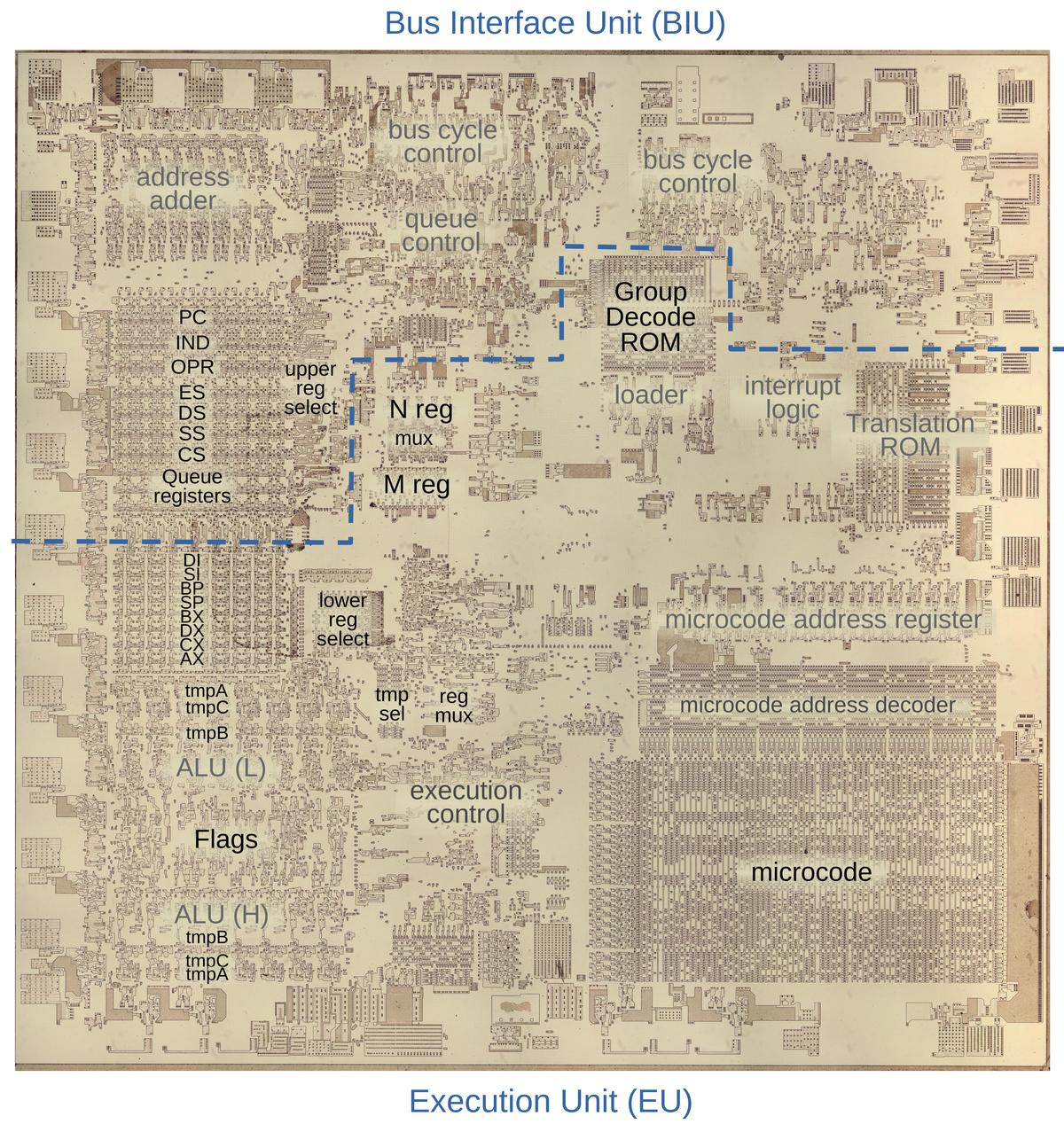
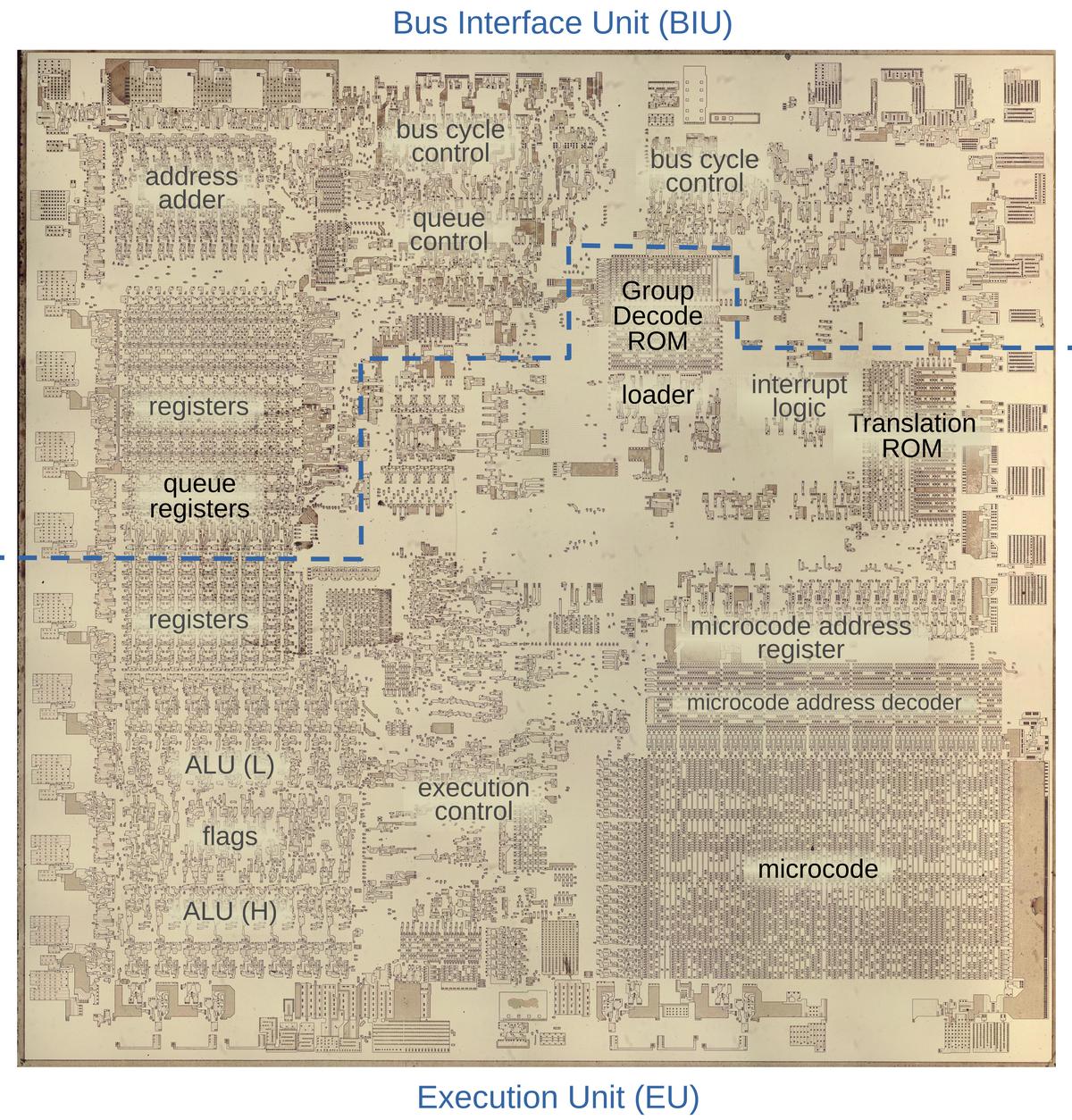
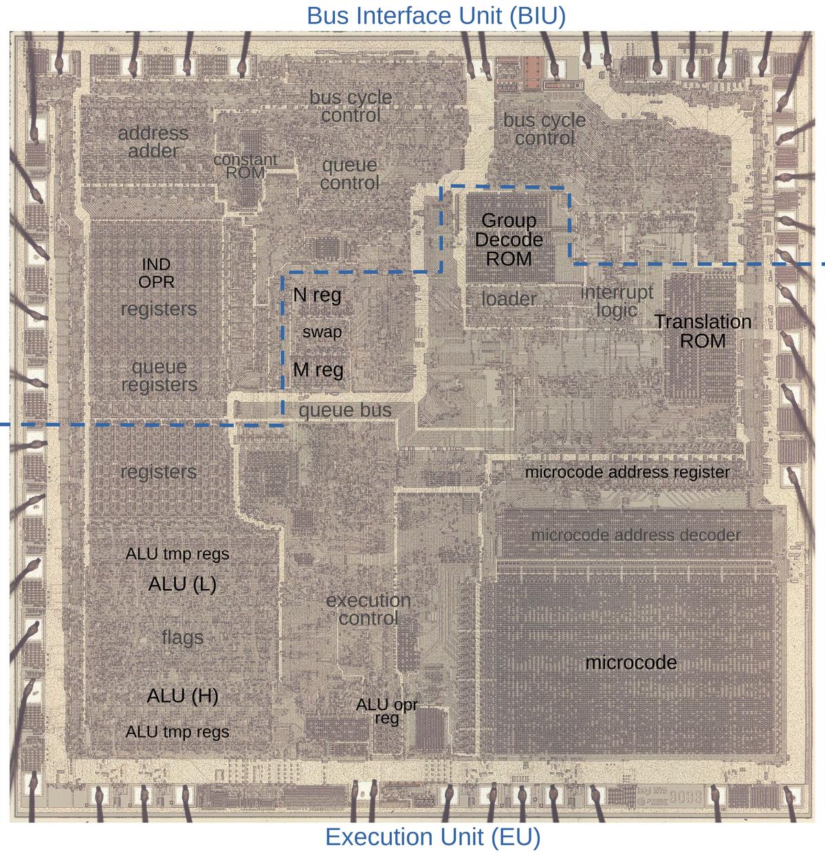
My analysis is based on reverse-engineering the 8086 from die photos. The die photo below shows the chip under a microscope. For this die photo, I removed the the metal and polysilicon layers, revealing the silicon underneath. I've labeled the key functional blocks; the ones that are important to this post are darker. In particular, the registers and the Arithmetic/Logic Unit (ALU) are at the left and the microcode ROM is in the lower right. Architecturally, the chip is partitioned into a Bus Interface Unit (BIU) at the top and an Execution Unit (EU) below. The BIU handles bus and memory activity as well as instruction prefetching, while the Execution Unit (EU) executes the instructions.

The 8086 die under a microscope, with main functional blocks labeled.  Click on this image (or any other) for a larger version.

The 8086 die under a microscope, with main functional blocks labeled. Click on this image (or any other) for a larger version.

Microcode

Most people think of machine instructions as the basic steps that a computer performs. However, many processors (including the 8086) have another layer of software underneath: microcode. With microcode, instead of building the control circuitry from complex logic gates, the control logic is largely replaced with code. To execute a machine instruction, the computer internally executes several simpler micro-instructions, specified by the microcode.

The 8086 uses a hybrid approach: although it uses microcode, much of the instruction functionality is implemented with gate logic. This approach removed duplication from the microcode and kept the microcode small enough for 1978 technology. In a sense, the microcode is parameterized. For instance, the microcode can specify a generic Arithmetic/Logic Unit (ALU) operation and a generic register. The gate logic examines the instruction to determine which specific operation to perform and the appropriate register.

A micro-instruction in the 8086 is encoded into 21 bits as shown below. Every micro-instruction has a move from a source register to a destination register, each specified with 5 bits; this encoding is the main topic of this blog post. The meaning of the remaining bits depends on the type field and can be anything from an ALU operation to a memory read or write to a change of microcode control flow. For more about 8086 microcode, see my microcode blog post.

The encoding of a micro-instruction into 21 bits. Based on NEC v. Intel: Will Hardware Be Drawn into the Black Hole of Copyright?

The encoding of a micro-instruction into 21 bits. Based on NEC v. Intel: Will Hardware Be Drawn into the Black Hole of Copyright?

Let's look at how the machine instruction XCHG AX,reg is implemented in microcode. This instruction exchanges AX with the register specified in the low 3 bits of the instruction.1 The microcode for this instruction consists of three micro-instructions, so the instruction takes three clock cycles. Each micro-instruction contains a move, which is the interesting part.2 The specified register is moved to the ALU's temporary B register, the AX register is moved to the specified register, and finally the temporary B is moved to AX, completing the swap.

 move       action
M → tmpB           XCHG AX,rw: move reg to tmpB
AX → M      NXT     move AX to reg, Next to last
tmpB → AX   RNI     move tmpB to AX, Run Next Instruction

The key part for this discussion is how M indicates the desired register. Suppose the instruction is XCHG AX,DX. The bottom three bits of the instruction are 010, indicating DX. During the first clock cycle of instruction execution, the opcode byte is transferred from the prefetch queue over the queue bus. The M register is loaded with the DX number (which happens to be 26), based on the bottom three bits of the instruction. After a second clock cycle, the microcode starts. The first micro-instruction puts M's value (26) onto the source bus and the number for tmpB (13) on the destination bus, causing the transfer from DX to tmpB. The second micro-instruction puts the AX number (24) onto the source bus and the M value (26) onto the destination bus, causing the transfer from AX to DX. The third micro-instruction puts tmpB number (13) onto the source bus and the AX number (24) onto the destination bus, causing the transfer from tmpB to AX.

Thus, the values on the source and destination bus control the data transfer during each micro-instruction. Microcode can either specify these values explicitly (as for AX and tmpB) or can specify the M register to use the register defined in the instruction. Thus, the same microcode implements all the XCHG instructions and the microcode doesn't need to know which register is involved.

The register encoding

The microcode above illustrated how different numbers specified different registers. The table below shows how the number 0-31 maps onto a register. Some numbers have a different meaning for a source register or a destination register; a slash separates these entries.

0ES8AL16AH24AX
1CS9CL17CH25CX
2SS10DL18DH(M)26DX
3DS11BL19BH(N)27BX
4PC12tmpA20Σ/tmpAL28SP
5IND13tmpB21ONES/tmpBL29BP
6OPR14tmpC22CR/tmpAH30SI
7Q/-15F23ZERO/tmpBH31DI

Most of these entries are programmer-visible registers: the segment registers are in green, the 8-bit registers in blue, and the 16-bit registers in red. Some internal registers and pseudo-registers are also accessible: IND (Indirect register), holding the memory address for a read or write; OPR (Operand register), holding the data for a read or write; Q (Queue), reading a byte from the instruction prefetch queue; ALU temporary registers A, B, and C, along with low (L) and (H) bytes; F, Flags register; Σ, the ALU output; ONES, all ones; CR, the three low bits of the microcode address; and ZERO, the value zero. The M and N entries can only be specified from microcode, taking the place of DH and BH.

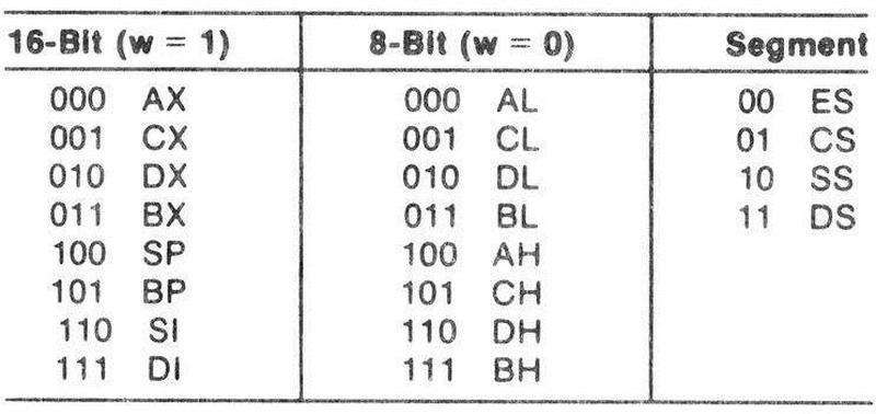
The table is kind of complicated, but there are reasons for its structure. First, machine instructions in the 8086 encode registers according to the system below. The 5-bit register number above is essentially an extension of the instruction encoding. Moreover, the AX/CX/DX/BX registers (red) are lined up with their upper-byte and lower-byte versions (blue). This simplifies the hardware since the low three bits of the register number select the register, while the upper two bits perform the byte versus word selection.3 The internal registers fit into available spots in the table.

The register assignments, from MCS-86 Assembly Language Reference Guide.

The register assignments, from MCS-86 Assembly Language Reference Guide.

The ModR/M byte

Many of the 8086 instructions use a second byte called the ModR/M byte to specify the addressing modes.4 The ModR/M byte gives the 8086 a lot of flexibility in how an instruction accesses its operands. The byte specifies a register for one operand and either a register or memory for the other operand. The diagram below shows how the byte is split into three fields: mod selects the overall mode, reg selects a register, and r/m selects either a register or memory mode. For a ModR/M byte, the reg and the r/m fields are read into the N and M registers respectively, so the registers specified in the ModR/M byte can be accessed by the microcode.

modregr/m
76543210

Let's look at the instruction SUB AX,BX which subtracts BX from AX. In the 8086, some important processing steps take place before the microcode starts. In particular, the "Group Decode ROM" categorizes the instruction into over a dozen categories that affect how it is processed, such as instructions that are implemented without microcode, one-byte instructions, or instructions with a ModR/M byte. The Group Decode ROM also indicates the structure of instructions, such as instructions that have a W bit selecting byte versus word operations, or a D bit reversing the direction of the operands. In this case, the Group Decode ROM classifies the instruction as containing a D bit, a W bit, an ALU operation, and a ModR/M byte.

Based on the Group Decode ROM's signals, fields from the opcode and ModR/M bytes are extracted and stored in various internal registers. The ALU operation type (SUB) is stored in the ALU opr register. The ModR/M byte specifies BX in the reg field and AX in the r/m field so the reg register number (BX, 27) is stored in the N register, and the r/m register number (AX, 24) is stored in the M register.

Once the preliminary decoding is done, the microcode below for this ALU instruction is executed.5 There are three micro-instructions, so the instruction takes three clock cycles. First, the register specified by M (i.e. AX) is moved to the ALU's temporary A register (tmpA). Meanwhile, XI configures the ALU to perform the operation specified by the instruction bits, i.e. SUB. The second micro-instruction moves the register specified by N (i.e. BX) to the ALU's tmpB register. The last micro-instruction stores the ALU's result (Σ, number 20) in the register indicated by M (i.e. AX).

  move       action
M → tmpA     XI tmpA   ALU rm↔r: AX to tmpA
N → tmpB     NXT       BX to tmpB
Σ → M        RNI F     result to AX, update flags

One of the interesting features of the 8086 is that many instructions contain a D bit that reverses the direction of the operation, swapping the source and the destination. If we keep the ModR/M byte but use the SUB instruction with the D bit set, the instruction becomes SUB BX,AX, subtracting AX from BX, the opposite of before. (Swapping the source and destination is more useful when one argument is in memory. But I'll use an example with two registers to keep it simple.) This instruction runs exactly the same microcode as before. The difference is that when the microcode accesses M, due to the direction bit it gets the value in N, i.e. BX instead of AX. The access to N is similarly swapped. The result is that AX is subtracted from BX, and the change of direction is transparent to the microcode.

The M and N registers

Now let's take a closer look at how the M and N registers are implemented. Each register holds a 5-bit register number, expanded from the three bits of the instruction. The M register is loaded from the three least significant bits of the instruction or ModR/M byte, while the N register is loaded with bits three through five. Most commonly, the registers are specified by the ModR/M byte, but some instructions specify the register in the opcode.6

The table below shows how the bits in the instruction's opcode or ModR/M byte (i5, i4, i3) are converted to a 5-bit number for the N register. There are three cases: a 16-bit register, an 8-bit register, and a segment register. The mappings below may seem random, but they result in the entries shown in the 5-bit register encoding table earlier. I've colored the entries so you can see the correspondence.

Mode43210
16-bit reg11i5i4i3
8-bit regi5i5'0i4i3
segment reg000i4i3

I'll go through the three cases in more detail. Many 8086 instructions have two versions, one that acts on bytes and one that acts on words, distinguished by the W bit (bit 0) in the instruction. If the Group Decode ROM indicates that the instruction has a W bit and the W bit is 0, then the instruction is a byte instruction.7 If the instruction has a ModR/M byte and the instruction operates on a byte, the N register is loaded with the 5-bit number for the specified byte register. This happens during "Second Clock", the clock cycle when the ModR/M byte is fetched from the instruction queue. The second case is similar; if the instruction operates on a word, the N register is loaded with the number for the word register specified in the ModR/M byte.

The third case handles a segment register. The N register is loaded with a segment register number during Second Clock if the Group Decode ROM indicates the instruction has a ModR/M byte with a segment-register field (specifically the segment register MOV instructions). A bit surprisingly, a segment register number is also loaded during First Clock. This supports the PUSH and POP segment register instructions, which have the segment register encoded in bits 3 and 4 of the opcode.8

The table below shows how the bits are assigned in the M register, which uses instruction bits i2, i1, and i0. The cases are a bit more complicated than the N register. First, a 16-bit register number is loaded from the opcode byte during First Clock to support instructions that specify the register in the low bits. During Second Clock, this value may be replaced.

For a ModR/M byte using register mode, the M register is reloaded with the specified 8-bit or a 16-bit register, depending on the byte mode signal described earlier. However, for a ModR/M byte that uses a memory mode, the M register is loaded with OPR (Operand), the internal register that holds the word that is read or written to memory.

Mode43210
16-bit reg11i2i1i0
8-bit regi2i2'0i1i0
OPR00110
AX/ALbyte'1000
convert to 8-bitm2m2'0m1m0

Many instructions use the AX or AL register, such as the ALU immediate instructions, the input and output instructions, and string instructions. For these, the Group Decode ROM triggers the AX or AL register number specifically to be loaded into the M register during Second Clock. The top bit is set for a word operation and cleared for a byte operation providing AX or AL as appropriate.

The final M register case is a bit tricky. For an immediate move instruction such as MOV BX,imm, bit 3 switches between a byte and a word move (rather than bit 0), because bits 2-0 specify the register. Unfortunately, the Group Decode ROM outputs aren't available during First Clock to indicate this case. Instead, M is loaded during First Clock with the assumption of a 16-bit register. If that turns out to be wrong, the M register is converted to an 8-bit register number during Second Clock by shuffling a few bits.

Producing the source and destination values

There are three cases for the number that goes on the source or destination buses: the register number can come from the micro-instruction, the value can come from the M or N register as specified in the micro-instruction, or the value can come from the M and N register with the roles swapped by the D bit. (Note that the source and destination can be different cases and are selected with separate circuitry.)

The first case is the default case, where the 5 bits from the micro-instruction source or destination specify the register directly. For instance, in the micro-instruction tmpB→AX, the microcode knows which registers are being used and specifies them directly.

The second and third cases involve more logic. Consider the source in M→tmpB. For an instruction without a D bit, the register number is taken from M. Likewise if the D bit is 0. But if the instruction uses a D bit and the D bit is 1, then the register number is taken from N. Multiplexers between the M and N registers select the appropriate register to put on the bus.

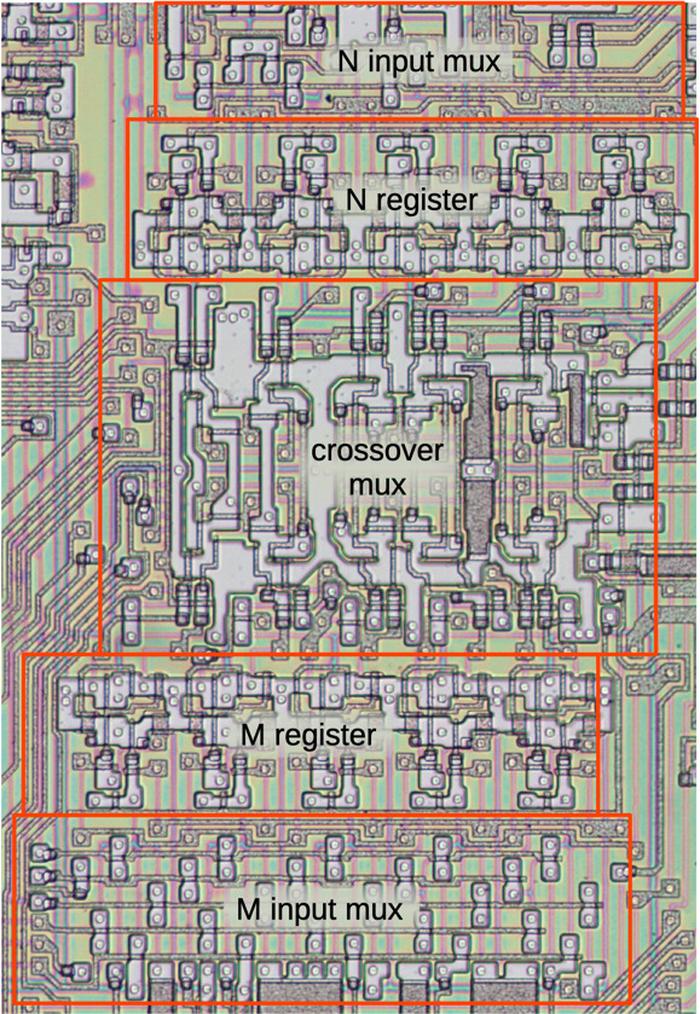
The M and N registers as they appear on the die. The metal layer has been removed from this image to show the silicon and polysilicon underneath.

The M and N registers as they appear on the die. The metal layer has been removed from this image to show the silicon and polysilicon underneath.

The diagram above shows how the M and N register circuitry is implemented on the die, with the N register at the top and the M register below. Each register has an input multiplexer that implements the tables above, selecting the appropriate 5 bits depending on the mode. The registers themselves are implemented as dynamic latches driven by the clock. In the middle, a crossover multiplexer drives the source and destination buses, selecting the M and N registers as appropriate and amplifying the signals with relatively large transistors. The third output from the multiplexer, the bits from the micro-instruction, is implemented in circuitry physically separated and closer to the microcode ROM.

The register selection hardware

How does the 5-bit number select a register? The 8086 has a bunch of logic that turns a register number into a control line that enables reading or writing of the register. For the most part, this logic is implemented with NOR gates that match a particular register number and generate a select signal. The signal goes through a special bootstrap driver to boost its voltage since it needs to control 16 register bits.

The 8086 registers are separated into two main groups. The "upper registers" are in the upper left of the chip, in the Bus Interface Unit. These are the registers that are directly involved with memory accesses. The "lower registers" are in the lower left of the chip, in the Execution Unit. From bottom to top, they are AX, CX, DX, BX, SP, BP, SI, and DI; their physical order matches their order in the instruction set.9 A separate PLA (Programmable Logic Array) selects the ALU temporary registers or flags as destination. Just below it, a PLA selects the source from ALU temporary registers, flags, or the ALU result (Σ).10 I've written about the 8086's registers and their low-level implementation here if you want more information.

Some history

The 8086's system of selecting registers with 3-bit codes originates with the Datapoint 2200,11 a desktop computer announced in 1970. The processor of the Datapoint 2200 was implemented with a board of TTL integrated circuits, since this was before microprocessors. Many of the Datapoint's instructions used a 3-bit code to select a register, with a destination register specification in bits 5-3 of the instruction and a source register in bits 2-0. (This layout is essentially the same as in 8086 instructions and the ModR/M byte.)12 The eight values of this code selected one of 7 registers, with the eighth value indicating a memory access. Intel copied the Datapoint 2200 architecture for the 800813 microprocessor (1972) and cleaned it up for the 8080 (1974), but kept the basic instruction layout and register/memory selection bits.

The 8086's use of a numbering system for all the registers goes considerably beyond this pattern, partly because its registers function both as general-purpose registers and special-purpose registers.14 Many instructions can act on the AX, BX, etc. registers interchangeably, treating them as general-purpose registers. But these registers each have their own special purposes for other instructions, so the microcode must be able to access them specifically. This motivates the 8086's approach where registers can be treated as general-purpose registers that are selected from instruction bits, or as special-purpose registers selected by the microcode.

The Motorola 68000 (1979) makes an interesting comparison to the 8086 since they were competitors. The 68000 uses much wider microcode (85-bit microinstructions compared to 21 bits in the 8086). It has two main internal buses, but instead of providing generic source and destination transfers like the 8086, the 68000 has a much more complicated system: about two dozen microcode fields that connect registers and other components to the bus in various ways.15

Conclusions

Internally, the 8086 represents registers with a 5-bit number. This is unusual compared to previous microprocessors, which usually selected registers directly from the instruction or control circuitry. Three factors motivated this design in the 8086. First, it used microcode, so a uniform method of specifying registers (both programmer-visible and internal) was useful. Second, being able to swap the source and destination in an instruction motivated a level of indirection in register specification, provided by the M and N registers. Finally, the flexibility of the ModR/M byte, in particular supporting byte, word, and segment registers, meant that the register specification needed 5 bits.

I've written multiple posts on the 8086 so far and plan to continue reverse-engineering the 8086 die so follow me on Twitter @kenshirriff or RSS for updates. I've also started experimenting with Mastodon recently as @oldbytes.space@kenshirriff.

Notes and references

  1. As an aside, the NOP instruction (no operation) in the 8086 is really XCHG AX,AX. Exchanging the AX register with itself accomplishes nothing but takes 3 clock cycles. 

  2. The action part of the micro-instructions indicates the second-last micro-instruction (NXT, next) and the last (RNI, Run Next Instruction), so execution of the next machine instruction can start. 

  3. Note that register #18 can refer both to DH and the destination register. This doesn't cause a conflict because it refers to DH if loaded from the instruction, and refers to the destination register if specified in the micro-instruction. The only issue is that a micro-instruction can't refer to the DH register explicitly (or the BH register similarly). This restriction isn't a problem because the microcode never needs to do this. 

  4. I discuss the 8086's ModR/M byte in detail here

  5. The microcode listings are based on Andrew Jenner's disassembly. I have made some modifications to (hopefully) make it easier to understand. 

  6. There are a few instructions that specify a register in the opcode rather than the ModR/M byte. For 16-bit registers, the INC, DEC, XCHG, PUSH, and POP instructions specify the register in the low three bits of the opcode. The MOV immediate instructions specify either an 8-bit or 16-bit register in the low three bits. On the other hand, the segment is specified by bits 3 and 4 of the segment prefixes, PUSH, and POP instructions. 

  7. A few instructions only have byte versions (DAA, AAA, DAS, AAS, AAM, AAD, XLAT). This is indicated by a Group Decode ROM output and forces instruction execution into byte mode. Thus, these instructions would load a byte register into N, but since these instructions don't have a register specification, it doesn't matter. 

  8. The segment prefixes use the same instruction bits (3 and 4) as PUSH and POP to select the segment register, so you might expect the prefixes to also load the N register. However, the prefixes are implemented in hardware, rather than microcode. Thus, they do not use the N register and the N register is not loaded with the segment register number. 

  9. You might wonder why the BX register is out of sequence with the other registers, both physically on the chip and in the instruction set. The 8086 was designed so 8080 assembly code could be translated to 8086 code. Originally, the 8086 registers had different names: XA, BC, DE, HL, SP, MP, IJ, and IK. The first four names matched the registers in the Intel 8080 processor, while MP was Memory Pointer and IJ and IK were Index registers. However, when the 8086 was released the registers were given names that corresponded to their functions in the 8086, abandoning the 8080 names. XA became the Accumulator AX, The BC register was used for counting, so it became the Count register CX. The DE register was a data register, so it became the Data register DX. The HL register was used as a base for memory accesses, so it became the Base register BX. The result is that the BX register ended up last.

    A program CONV-86 allowed 8080 assembly programs to be translated into 8086 assembly programs, with 8080 registers replaced with the corresponding 8086 registers. The old 8086 register names can be seen in the 8086 patent, while the Accumulator, Base, Count, Data names are in the MCS-86 Assembly Language Reference Guide. See also this Stack Exchange discussion

  10. The all-ones source doesn't have any decoding; the ALU bus is precharged to the high state, so it is all ones by default. 

  11. The system of using bit fields in instructions to select registers is much older, of course. The groundbreaking IBM System/360 architecture (1964), for instance, used 4-bit fields in instructions to select one of the 16 general-purpose registers. 

  12. Note that with this instruction layout, the instruction set maps cleanly onto octal. The Datapoint 2200 used octal to describe the instruction set, but Intel switched to hexadecimal for its processors. Hexadecimal was becoming more popular than octal at the time, but the move to hexadecimal hides most of the inherent structure of the instructions. See x86 is an octal machine for details. 

  13. The Datapoint manufacturer talked to Intel and Texas Instruments about replacing the board of chips with a single processor chip. Texas Instruments produced the TMX 1795 microprocessor chip and Intel produced the 8008 shortly after, both copying the Datapoint 2200's architecture and instruction set. Datapoint didn't like the performance of these chips and decided to stick with a TTL-based processor. Texas Instruments couldn't find a customer for the TMX 1795 and abandoned it. Intel, on the other hand, sold the 8008 as an 8-bit microprocessor, creating the microprocessor market in the process. Register selection in these processors was pretty simple: the 3 instruction bits were decoded into 8 select lines that selected the appropriate register (or memory). Since these processors had hard-coded control instead of microcode, the control circuity generated other register selection lines directly. 

  14. While the 8086 has eight registers that can be viewed as general-purpose, they all have some specific purposes. The AX register acts as the accumulator and has several special functions, such as its use in the XCHG (Exchange) operation, I/O operations, multiplication, and division. The BX register has a special role as a base register for memory accesses. The CX register acts as the counter for string operations and for the JCXZ (Jump if CX Zero) instruction. The DX register can specify the port for I/O operations and is used for CWD (Convert Word to Doubleword) and in multiplication and division. The SP register has a unique role as the stack pointer. The SI and DI registers are used as index registers for string operations and memory accesses. Finally, the BP register has a unique role as base pointer into the stack segment. On the 8-bit side, AX, BX, CX, and DX can be accessed as 8-bit registers, while the other registers cannot. The 8-bit AL register is used specifically for XLAT (Translate) while AH is used for the flag operations LAHF and SAHF. Thus, the 8086's registers are not completely orthogonal, and each one has some special cases, often for historical reasons. 

  15. Another way of looking at the Motorola 68000's microcode is that the register controls come from "horizontal" microcode, a micro-instruction with many bits, and fields that control functional elements directly. The 8086's microcode is more "vertical"; the micro-instructions have relatively few bits and the fields are highly encoded. In particular, the 8086's source and destination register fields are highly encoded, while the 68000 has fields that control the connection of an individual register to the bus. 

Reverse-engineering the electronics in the Globus analog navigational computer

In the Soyuz space missions, cosmonauts tracked their position above the Earth with a remarkable electromechanical device with a rotating globe. This navigation instrument was an analog computer that used an elaborate system of gears, cams, and differentials to compute the spacecraft's position. Officially, the unit was called a "space navigation indicator" with the Russian acronym ИНК (INK),1 but I'll use the nickname "Globus".

The INK-2S "Globus" space navigation indicator.

The INK-2S "Globus" space navigation indicator.

We recently received a Globus from a collector and opened it up for repair and reverse engineering. Although the Globus does all its calculations mechanically, it has some electronics to control the motors. Inconveniently, all the wires in the wiring harness to the external connector had been cut so I had to do some reverse engineering before we could power it up. In this blog post, I explain how the electronics operate. (For an overview of the mechanical components inside the Globus, see my previous article.)

A closeup of the gears inside the Globus. It performed calculations with gears, cams, and differentials.

A closeup of the gears inside the Globus. It performed calculations with gears, cams, and differentials.

Functionality

The primary purpose of the Globus is to indicate the spacecraft's position. The globe rotated while fixed crosshairs on the plastic dome indicated the spacecraft's position. Thus, the globe matched the cosmonauts' view of the Earth, allowing them to confirm their location. Latitude and longitude dials next to the globe provided a numerical indication of location. The light/shadow dial at the bottom showed when the spacecraft would be illuminated by the sun or in shadow.

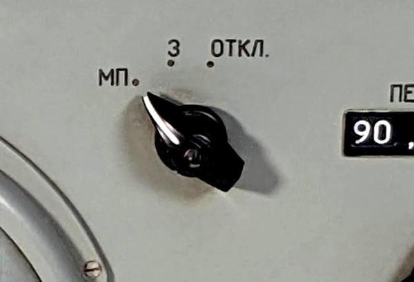
The mode of the Globus is controlled by a three-position rotary switch near the top of the Globus. The middle position "З" (Земля, Earth) shows the position of the spacecraft over the Earth. The left position, "МП" (место посадки, landing site) selects the landing position mode. The third position "Откл" (off) turns off most of the Globus. This rotary switch is surprisingly complicated with three wafers, each with two poles. Most of the electronics go through this switch, so this switch will appear often in the schematics below.

The rotary switch to select the landing angle mode.

The rotary switch to select the landing angle mode.

In the landing position mode, the Globus rotates to show where the spacecraft would land if you fired the retrorockets now. This allowed the cosmonauts to evaluate the suitability of this landing site. This position is computed simply by rapidly rotating the globe through a fraction of an orbit, since the landing position will be on the current orbital track. Most of the electronics in the Globus control the motor that performs this rotation.

Overview of the electronics

The Globus is primarily mechanical, but it has more electrical and electronic components than you might expect. The mechanical motion is powered by two solenoids with ratchets to turn gears. The landing site mode is implemented with a motor to rotate to the landing position, controlled by two limit switches. An electroluminescent light indicates the landing position mode. A potentiometer provides position feedback to external devices.

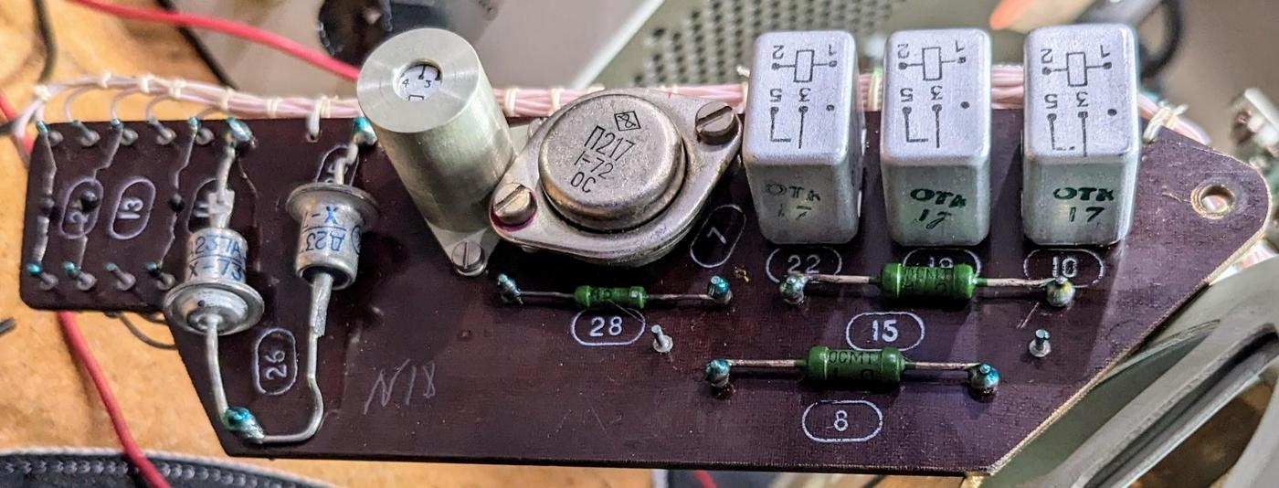
To control these components, the Globus has an electronics board with four relays, along with a germanium power transistor and some resistors and diodes.2 Bundles of thin white wires with careful lacing connect the electronics board to the other components.

The electronics circuit board.

The electronics circuit board.

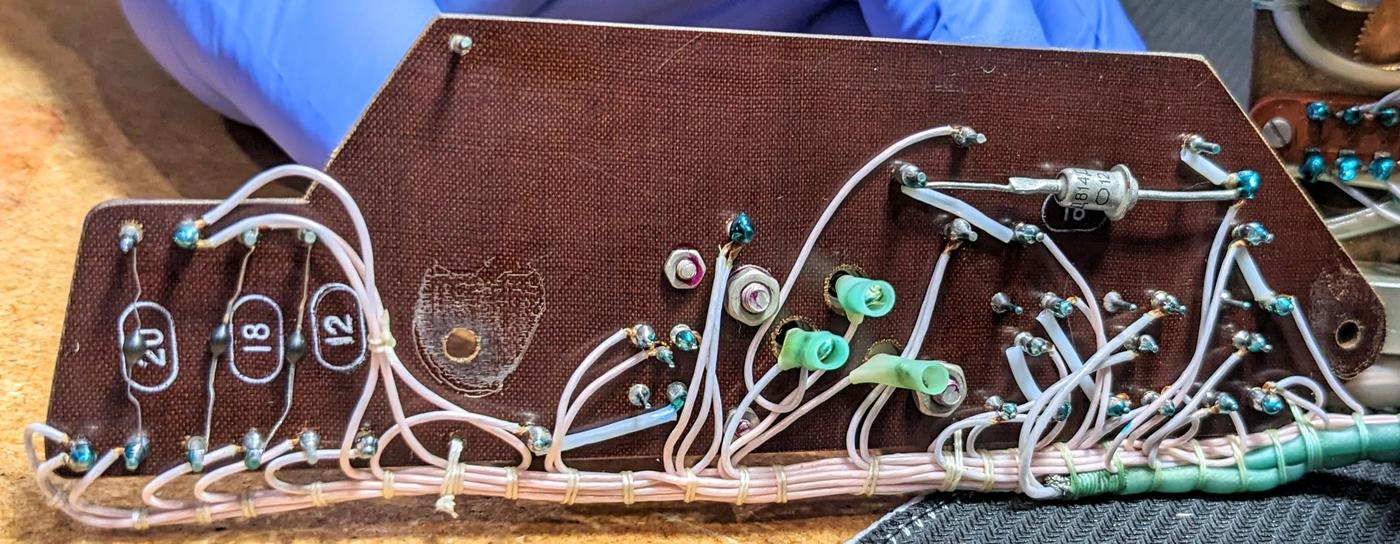
The back of the circuit board has a few more diodes. The wiring is all point-to-point; it is not a printed-circuit board. I will explain the circuitry in more detail below.

The back of the circuit board.

The back of the circuit board.

The drive solenoids

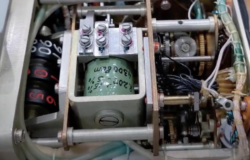
The green cylinder at the front is the upper solenoid, driving the orbital motion. The digit wheels to indicate orbital time are at the left.

The green cylinder at the front is the upper solenoid, driving the orbital motion. The digit wheels to indicate orbital time are at the left.

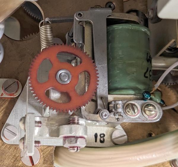
The Globus contains two ratchet solenoids: one for the orbital rotation and one for the Earth's rotation. The complex gear trains and the motion of the globe are driven by these solenoids. These solenoids take 1-hertz pules of 27 volts and 100ms duration. Each pulse causes the solenoid to advance the gear by one tooth; a pawl keeps the gear from slipping back. These small rotations drive the gears throughout the Globus and result in a tiny movement of the globe.

The lower driving solenoid powers the Earth rotation.

The lower driving solenoid powers the Earth rotation.

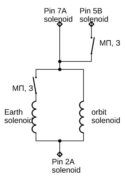
As the schematic shows, the solenoids are controlled by two switches that are closed in the МП (landing position) and З (Earth orbit) modes. The solenoids are powered through three pins. The wiring doesn't entirely make sense to me. If powered through pins 2A and 7A, the Earth motor is switched while the orbit motor is always powered. But if powered through pins 2A and 5B, both motors are switched. Maybe pin 7A monitors the on/off status of the Globus.

Schematic diagram of the solenoid wiring.

Schematic diagram of the solenoid wiring.

By powering the solenoids with 1 hertz pulses, we caused the Globus to rotate. The motion is very slow (90 minutes for an orbit and one day for the Earth's rotation), so we tried overclocking it at 10 hertz. This made the motion barely visible; Marc used a time-lapse to speed it up in the video below.

The landing location mechanism

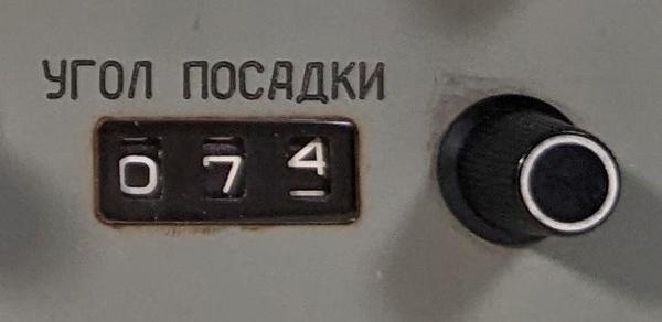
The Globus can display where the spacecraft would land if you started a re-entry burn now, with an accuracy of 150 km. This is computed by projecting the current orbit forward for a particular distance, specified as an angle. The cosmonaut specifies this value with the landing angle knob (details). Rotating the globe to this new position is harder than you might expect, using a motor, limit switches, and the majority of the electronics in the Globus.

The landing angle control.

The landing angle control.

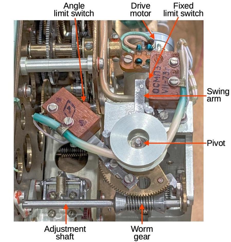
The landing angle knob pivots the angle limit switch, shown below. The swing arm moves as the globe rotates to the landing position and hits the angle limit switch when the landing position is reached. When returning to Earth orbit mode, the swing arm swings back until it hits the fixed limit switch. Thus, the globe is rotated by the selected amount when displaying the landing position.

The landing angle function uses a complex mechanism.

The landing angle function uses a complex mechanism.

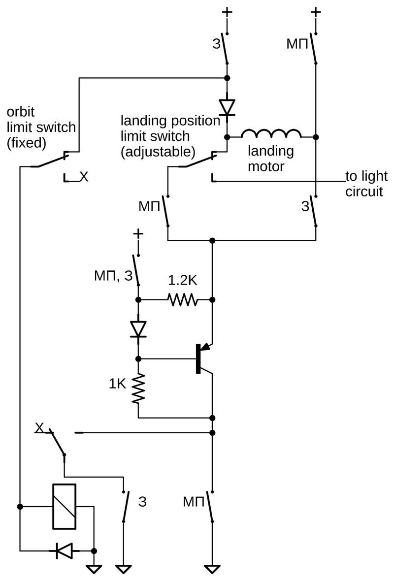
To control the motor, the rotary switch reverses the DC motor based on the mode, while the limit switches and power transistor turn the motor on and off. In landing position mode (МП), the motor spins the globe forward. The mode switch controls the direction of current flow: from upper right, through the motor, through the angle limit switch, through the transistor, and to ground at the bottom. The motor will rotate the globe and the arm until it hits the "landing position" limit switch, cutting power to the motor and activating the path to the light circuit, which I will discuss below. The diode prevents current flowing backward through the motor to the relay. The power transistor apparently acts as a current sink, regulating the current through the motor.

Schematic diagram of the landing location mechanism.

Schematic diagram of the landing location mechanism.

In Earth orbit mode (З), the motor spins the globe back to its regular position. The mode switch reverses the current flow through the motor: from the upper-left, through the diode and the motor, and out the lower-right to the transistor. At the bottom, the relay completes the circuit until the moving arm hits the fixed orbit limit switch. This opens the normally-closed contact, cutting power to the relay, opening the relay contact, and stopping the motor.

The landing place light

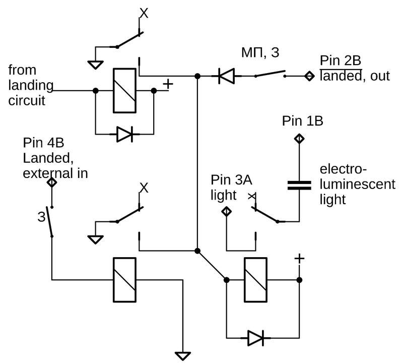
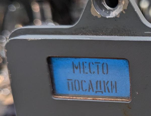
The upper-left corner of the Globus has an electroluminescent light labeled "Место посадки" (Landing place). This light illuminates when the globe indicates the landing place rather than the orbital position. The light is powered by AC provided on two external pins and is controlled by two relays. One relay is activated by the landing circuit described above, when the limit switch closes. The second relay is driven by an external pin. I don't know if this is for a "lamp test" or control from an external system.

Schematic diagram of the circuitry that controls the electroluminescent light.

Schematic diagram of the circuitry that controls the electroluminescent light.

We powered the light with an EL inverter from Adafruit, which produces 100 VAC at 2KHz, perhaps. The spacecraft used a "Static Inverter" to power the light, but I don't have any details on it. The display provides a nice blue glow.

The landing position indicator, illuminated.

The landing position indicator, illuminated.

The potentiometer

A 360° potentiometer (below) converts the spacecraft's orbital position into a resistance. Sources indicate that the Globus provides this signal to other units on the spacecraft, but I don't know specifically what these devices are. The potentiometer appears to linearly track the spacecraft's position through the orbital cycle. Note that this is not the same as the latitude, which oscillates, or the longitude, which is non-linear.

The potentiometer converts the orbital position into a voltage.
To the right is the cam that produces the longitude display. Antarctica is visible on the globe.

The potentiometer converts the orbital position into a voltage. To the right is the cam that produces the longitude display. Antarctica is visible on the globe.

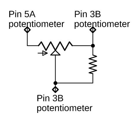
As the schematic below shows, the potentiometer has a resistor on one leg for some reason.

Schematic diagram of the orbital-position potentiometer.

Schematic diagram of the orbital-position potentiometer.

The external connector

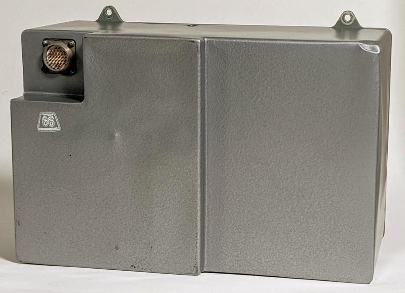
To connect the Globus to the rest of the spacecraft, the back of the Globus has a 32-pin connector, a standard RS32TV Soviet military design.

The back of the Globus, with the connector at the upper left.

The back of the Globus, with the connector at the upper left.

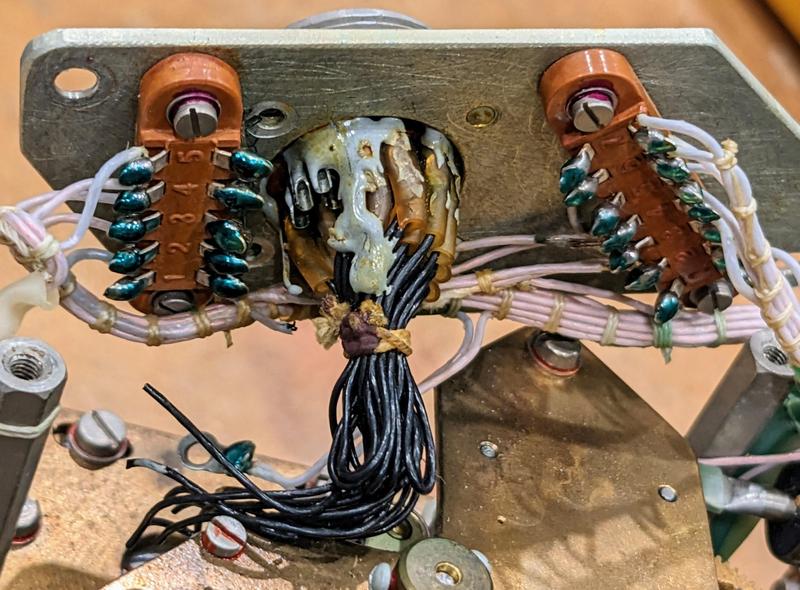
The connector was wired to nearby 5-pin and 7-pin terminal strips. In the schematics, I label these connectors as "B" and "A" respectively. Inconveniently, all the wires to the box's external connector were cut (the black wires), perhaps to decommission the unit. The pinout of the external connector is unknown so we can't easily reconnect the wires.

A closeup of the back of the connector showing the cut black wires.

A closeup of the back of the connector showing the cut black wires.

Conclusions

By tracing out the wiring of the Globus, I determined its circuitry. This was more difficult than expected, since the wiring consists of bundles of identical white wires. Moreover, many things go through the mode switch, and its terminals were inaccessible. Between the mode switch and the limit switches, there were many cases to check.

Once I determined the circuitry, we could power up the Globus. So far, we have powered the solenoids to turn the Globus. We also illuminated the landing position light. Finally, we ran the landing position motor.

Follow me on Twitter @kenshirriff or RSS for updates. I've also started experimenting with Mastodon recently as @oldbytes.space@kenshirriff. Many thanks to Marcel for providing the Globus.

Notes and references

  1. In Russian, the name for the device is "Индикатор Навигационный Космический" abbreviated as ИНК (INK). This translates to "space navigation indicator." 

  2. Most of the diodes are flyback diodes, two diodes in series across each relay coil to eliminate the inductive kick when the coil is disconnected. 

How the 8086 processor determines the length of an instruction

The Intel 8086 processor (1978) has a complicated instruction set with instructions ranging from one to six bytes long. This raises the question of how the processor knows the length of an instruction.1 The answer is that the 8086 uses an interesting combination of lookup ROMs and microcode to determine how many bytes to use for an instruction. In brief, the ROMs perform enough decoding to figure out if it needs one byte or two. After that, the microcode simply consumes instruction bytes as it needs them. Thus, nothing in the chip explicitly "knows" the length of an instruction. This blog post describes this process in more detail.

The die photo below shows the chip under a microscope. I've labeled the key functional blocks; the ones that are important to this post are darker. Architecturally, the chip is partitioned into a Bus Interface Unit (BIU) at the top and an Execution Unit (EU) below. The BIU handles bus and memory activity as well as instruction prefetching, while the Execution Unit (EU) executes the instructions.

The 8086 die under a microscope, with main functional blocks labeled. This photo shows the chip with the metal and polysilicon removed, revealing the silicon underneath. Click on this image (or any other) for a larger version.

The 8086 die under a microscope, with main functional blocks labeled. This photo shows the chip with the metal and polysilicon removed, revealing the silicon underneath. Click on this image (or any other) for a larger version.

The prefetch queue, the loader, and the microcode

The 8086 uses a 6-byte instruction prefetch queue to hold instructions, and this queue will play an important role in this discussion.3 Earlier microprocessors read instructions from memory as they were needed, which could cause the CPU to wait on memory. The 8086, instead, read instructions from memory before they were needed, storing them in the instruction prefetch queue. (You can think of this as a primitive instruction cache.) To execute an instruction, the 8086 took bytes out of the queue one at a time. If the queue ran empty, the processor waited until more instruction bytes were fetched from memory into the queue.

A circuit called the loader handles the interaction between the prefetch queue and instruction execution. The loader is a small state machine that provides control signals to the rest of the execution circuitry. The loader gets the first byte of an instruction from the prefetch queue and issues a signal FC (First Clock) that starts execution of the instruction.

At this point, the Group Decode ROM performs the first stage of instruction decoding, classifying the instruction into various categories based on the opcode byte. Most of the 8086's instructions are implemented in microcode. However, a few instructions are so simple that they are implemented with logic circuits. For example, the CLC (Clear Carry) instruction clears the carry flag directly. The Group Decode ROM categorizes these instructions as 1BL (one-byte, implemented in logic). The loader responds by issuing an SC (Second Clock) signal to wrap up execution and start the next instruction. Thus, these simple instructions take two clock cycles.

The 8086 has various prefix bytes that can be put in front of an instruction to change its behavior. For instance, a segment prefix changes the memory segment that the instruction uses. A LOCK prefix locks the bus during the next instruction. The Group Decode ROM detects a prefix and outputs a prefix signal. This causes the prefix to be handled in logic, rather than microcode, similar to the 1BL instructions. Thus, a prefix also takes one byte and two clock cycles.

The remaining instructions are handled by microcode.2 Let's start with a one-byte instruction such as INC AX, which increments the AX register. As before, the loader gets the instruction byte from the prefix queue. The Group Decode ROM determines that this instruction is implemented in microcode and can start after one byte, so the microcode engine starts running. The microcode below handles the increment and decrement instructions. It moves the appropriate register, indicated by M to the ALU's temporary B register. It puts the incremented or decremented result (Σ) back into the register (M). RNI tells the loader to run the next instruction. With two micro-instruction, this instruction takes two clock cycles.

M → tmpB        XI tmpB, NX INC/DEC: get value from M, set up ALU
Σ → M           WB,RNI F     put result in M, run next instruction

But what happens with an instruction that is more than one byte long, such as adding an immediate value to a register? Let's look at ADD AX,1234, which adds 1234 to the AX register. As before, the loader reads one byte and then the microcode engine starts running. At this point, the 8086 doesn't "realize" that this is a 3-byte instruction. The first line of the microcode below gets one byte of the immediate operand: Q→tmpBL loads a byte from the instruction prefetch queue into the low byte of the temporary B register. Similarly, the second line loads the second byte. The next line puts the register value (M) in tmpA. The last line puts the sum back into the register and runs the next instruction. Since this instruction takes two bytes from the prefetch queue, it is three bytes long in total. But nothing explicitly indicates this instruction is three bytes long.

Q → tmpBL       JMPS L8 2  alu A,i: get byte from queue
Q → tmpBH                   get byte from queue
M → tmpA        XI tmpA, NX get value from M, set up ALU
Σ → M           WB,RNI F    put result in M, run next instruction

You can also add a one-byte immediate value to a register, such as ADD AL,12. This uses the same microcode above. However, in the first line, JMPS L8 is a conditional jump that skips the second micro-instruction if the data length is 8 bits. Thus, the microcode only consumes one byte from the prefetch queue, making the instruction two bytes long. In other words, what makes this instruction two bytes instead of three is the bit in the opcode which triggers the conditional jump in the microcode.

The 8086 has another class of instructions, those with a ModR/M byte following the opcode. The Group Decode ROM classifies these instructions as 2BR (two-byte ROM) indicating that the second byte must be fetched before processing by the microcode ROM. For these instructions, the loader fetches the second byte from the prefetch queue before triggering the SC (Second Clock signal) to start microcode execution.

The ModR/M byte indicates the addressing mode that the instruction should use, such as register-to-register or memory-to-register. The ModR/M can change the instruction length by specifying an address displacement of one or two bytes. A second ROM called the Translation ROM selects the appropriate microcode for the addressing mode (details). For example, if the addressing mode includes an address displacement, the microcode below is used:

Q → tmpBL   JMPS MOD1 12 [i]: get byte(s)
Q → tmpBH         
Σ → tmpA    BX EAFINISH 12: add displacement

This microcode fetches two displacement bytes from the prefetch queue (Q). However, if the ModR/M byte specifies a one-byte displacement, the MOD1 condition causes the microcode to jump over the second fetch. Thus, this microcode uses one or two additional instruction bytes depending on the value of the ModR/M byte.

To summarize, nothing in the 8086 "knows" how long an instruction is. The Group Decode ROM makes part of the decision, classifying instructions as a prefix, 1-byte logic, 2-byte ROM, or otherwise, causing the loader to fetch one or two bytes. The microcode then consumes instruction bytes as needed. In the end, the length of an 8086 instruction is determined by how many bytes are taken from the prefetch queue by the time it ends.

Some other systems

It's interesting to see how other processors deal with instruction length. For example, RISC processors (Reduced Instruction Set Computers) typically have fixed-length instructions. For instance, the ARM-1 processor used 32-bit instructions, making instruction decoding very simple.

Early microprocessors such as the MOS Technology 6502 (1975) didn't use microcode, but were controlled by state machines. The CPU fetches instruction bytes from memory as needed, as it moves through various execution states. Thus, as with the 8086, the length of an instruction wasn't explicit, but was how many bytes it used.

The IBM 1401 computer (1959) took a completely different approach with its variable-length words. Each character in memory had an associated "word mark" bit, which you can think of as a metadata bit. Each machine instruction consisted of a variable number of characters with a word mark on the first one. Thus, the processor could read instruction characters until it hit a word mark, which indicated the start of the next instruction. The word mark explicitly indicated to the processor how long each instruction was.

Perhaps the worst approach for variable-length instructions was the Intel iAPX 432 processor (1981), which had instructions with variable bit lengths, from 6 to 321 bits long. As a result, instructions weren't aligned on byte boundaries, making instruction decoding even more inconvenient. This was just one of the reasons that the iAPX 432 ended up overly complicated, years behind schedule, and a commercial failure.

The 8086's variable-length instructions led to the x86 architecture, with instructions from 1 to 15 bytes long. This is particularly inconvenient with modern superscalar processors that run multiple instructions in parallel. The problem is that the processor must break the instruction stream into individual instructions before they execute. The Intel P6 microarchitecture used in the Pentium Pro (1995) has instruction decoders to decode the instruction stream into micro-operations.4 It starts with an "instruction length block" that analyzes the first bytes of the instruction to determine how long it is. (This is not a straightforward task to perform rapidly on multiple instructions in parallel.) The "instruction steering block" uses this information to break the byte stream into instructions and steer instructions to the decoders.

The AMD K6 3D processor (1999) had predecode logic that associated 5 predecode bits with each instruction byte: three pointed to the start of the next instruction, one indicated the length depended on a D bit, and one indicated the presence of a ModR/M byte. This logic examined up to three bytes to make its decisions. Instructions were split apart and assigned to decoders based on the predecode bits. In some cases, the predecode logic gave up and flagged the instruction as "unsuccessfully predecoded", for instance an instruction longer than 7 bytes. These instructions were handled by a slower path.

Conclusions

The 8086 processor has instructions with a variety of lengths, but nothing in the processor explicitly determines the length. Instead, an instruction uses as many bytes as it needs. (That sounds sort of tautological, but I'm not sure how else to put it.) The Group Decode ROM makes an initial classification, the Translation ROM determines the addressing mode, and the microcode consumes bytes as needed.

While this approach gave the 8086 a flexible instruction set, it created a problem in the long run for the x86 architecture, requiring complicated logic to determine instruction length. One benefit of RISC-based processors such as the Apple M1 is that they have (mostly) constant instruction lengths, making instruction decoding faster and simpler.

I've written multiple posts on the 8086 so far and plan to continue reverse-engineering the 8086 die so follow me on Twitter @kenshirriff or RSS for updates. I've also started experimenting with Mastodon recently as @oldbytes.space@kenshirriff.

Notes and references

  1. I was inspired to investigate instruction length based on a Stack Overflow question

  2. I'll just give a brief overview of microcode here. Each micro-instruction is 21 bits long, as shown below. A micro-instruction specifies a move between a source register and destination register. It also has an action that depends on the micro-instruction type. For more details, see my post on the 8086 microcode pipeline.

    The encoding of a micro-instruction into 21 bits. Based on NEC v. Intel: Will Hardware Be Drawn into the Black Hole of Copyright?

    The encoding of a micro-instruction into 21 bits. Based on NEC v. Intel: Will Hardware Be Drawn into the Black Hole of Copyright?


  3. The 8088 processor, used in the original IBM PC, has a smaller 4-byte prefetch queue. The 8088 is almost the same as the 8086, except it has an 8-bit external bus instead of a 16-bit external bus. This makes memory accesses (including prefetches) slower, so a smaller prefetch queue works better. 

  4. The book Modern Processor Design discusses the P6 microarchitecture in detail. The book The Anatomy of a High-Performance Microprocessor discusses the AMD K5 3D processor in even more detail; see chapter 2. 

Reverse-engineering the ModR/M addressing microcode in the Intel 8086 processor

One interesting aspect of a computer's instruction set is its addressing modes, how the computer determines the address for a memory access. The Intel 8086 (1978) used the ModR/M byte, a special byte following the opcode, to select the addressing mode.1 The ModR/M byte has persisted into the modern x86 architecture, so it's interesting to look at its roots and original implementation.

In this post, I look at the hardware and microcode in the 8086 that implements ModR/M2 and how the 8086 designers fit multiple addressing modes into the 8086's limited microcode ROM. One technique was a hybrid approach that combined generic microcode with hardware logic that filled in the details for a particular instruction. A second technique was modular microcode, with subroutines for various parts of the task.

I've been reverse-engineering the 8086 starting with the silicon die. The die photo below shows the chip under a microscope. The metal layer on top of the chip is visible, with the silicon and polysilicon mostly hidden underneath. Around the edges of the die, bond wires connect pads to the chip's 40 external pins. I've labeled the key functional blocks; the ones that are important to this discussion are darker and will be discussed in detail below. Architecturally, the chip is partitioned into a Bus Interface Unit (BIU) at the top and an Execution Unit (EU) below. The BIU handles bus and memory activity as well as instruction prefetching, while the Execution Unit (EU) executes instructions and microcode. Both units play important roles in memory addressing.

The 8086 die under a microscope, with main functional blocks labeled. This photo shows the chip's single metal layer; the polysilicon and silicon are underneath. Click on this image (or any other) for a larger version.

The 8086 die under a microscope, with main functional blocks labeled. This photo shows the chip's single metal layer; the polysilicon and silicon are underneath. Click on this image (or any other) for a larger version.

8086 addressing modes

Let's start with an addition instruction, ADD dst,src, which adds a source value to a destination value and stores the result in the destination.3 What are the source and destination? Memory? Registers? The addressing mode answers this question.

You can use a register as the source and another register as the destination. The instruction below uses the AX register as the destination and the BX register as the source. Thus, it adds BX to AX and puts the result in AX.

ADD AX, BX           Add the contents of the BX register to the AX register

A memory access is indicated with square brackets around the "effective address"4 to access. For instance, [1234] means the memory location with address 1234, while [BP] means the memory location that the BP register points to. For a more complicated addressing mode, [BP+SI+1234] means the memory location is determined by adding the BP and SI registers to the constant 1234 (known as the displacement). On the 8086, you can use memory for the source or the destination, but not both. Here are some examples of using memory as a source:

ADD AX, [1234]       Add the contents of memory location 1234 to AX register
ADD CX, [BP]         Add memory pointed to by BP register to CX register
ADD DX, [BX+SI+1234] Source memory address is BX + SI + constant 1234

Here are examples with memory as the destination:

ADD [1234], AX       Add AX to the contents of memory location 1234
ADD [BP], CX         Add CX to memory pointed to by BP register
ADD [BX+SI+1234], DX Destination memory address is BX + SI + constant 1234

You can also operate on bytes instead of words, using a byte register and accessing a memory byte:

ADD AL, [SI+1234]    Add to the low byte of AX register
ADD AH, [BP+DI+1234] Add to the high byte of AX register

As you can see, the 8086 supports many different addressing schemes. To understand how they are implemented, we must first look at how instructions encode the addressing schemes in the ModR/M byte.

The ModR/M byte

The ModR/M byte follows many opcodes to specify the addressing mode. This byte is fairly complicated but I'll try to explain it in this section. The diagram below shows how the byte is split into three fields:5 mod selects the overall mode, reg selects a register, and r/m selects either a register or memory mode.

modregr/m
76543210

I'll start with the register-register mode, where the mod bits are 11 and the reg and r/m fields each select one of eight registers, as shown below. The instruction ADD AX,BX would use reg=011 to select BX and r/m=000 to select AX, so the ModR/M byte would be 11011000. (The register assignment depends on whether the instruction operates on words, bytes, or segment registers. For instance, in a word instruction, 001 selects the CX register, while in a byte instruction, 001 selects the CL register, the low byte of CX.)

The register assignments, from MCS-86 Assembly Language Reference Guide.

The register assignments, from MCS-86 Assembly Language Reference Guide.

The next addressing mode specifies a memory argument and a register argument. In this case, the mod bits are 00, the reg field specifies a register as described above, and the r/m field specifies a memory address according to the table below. For example, the instruction ADD [SI],CX would use reg=001 to select CX and r/m=100 to select [SI], so the ModR/M byte would be 00001100.

r/mOperand Address
000[BX+SI]
001[BX+DI]
010[BP+SI]
011[BP+DI]
100[SI]
101[DI]
110[BP]
111[BX]

The next mode, 01, adds an 8-bit signed displacement to the address. This displacement consists of one byte following the ModR/M byte. This supports addressing modes such as [BP+5]. The mode 10 is similar except the displacement is two bytes long, for addressing modes such as [BP+DI+0x1234].

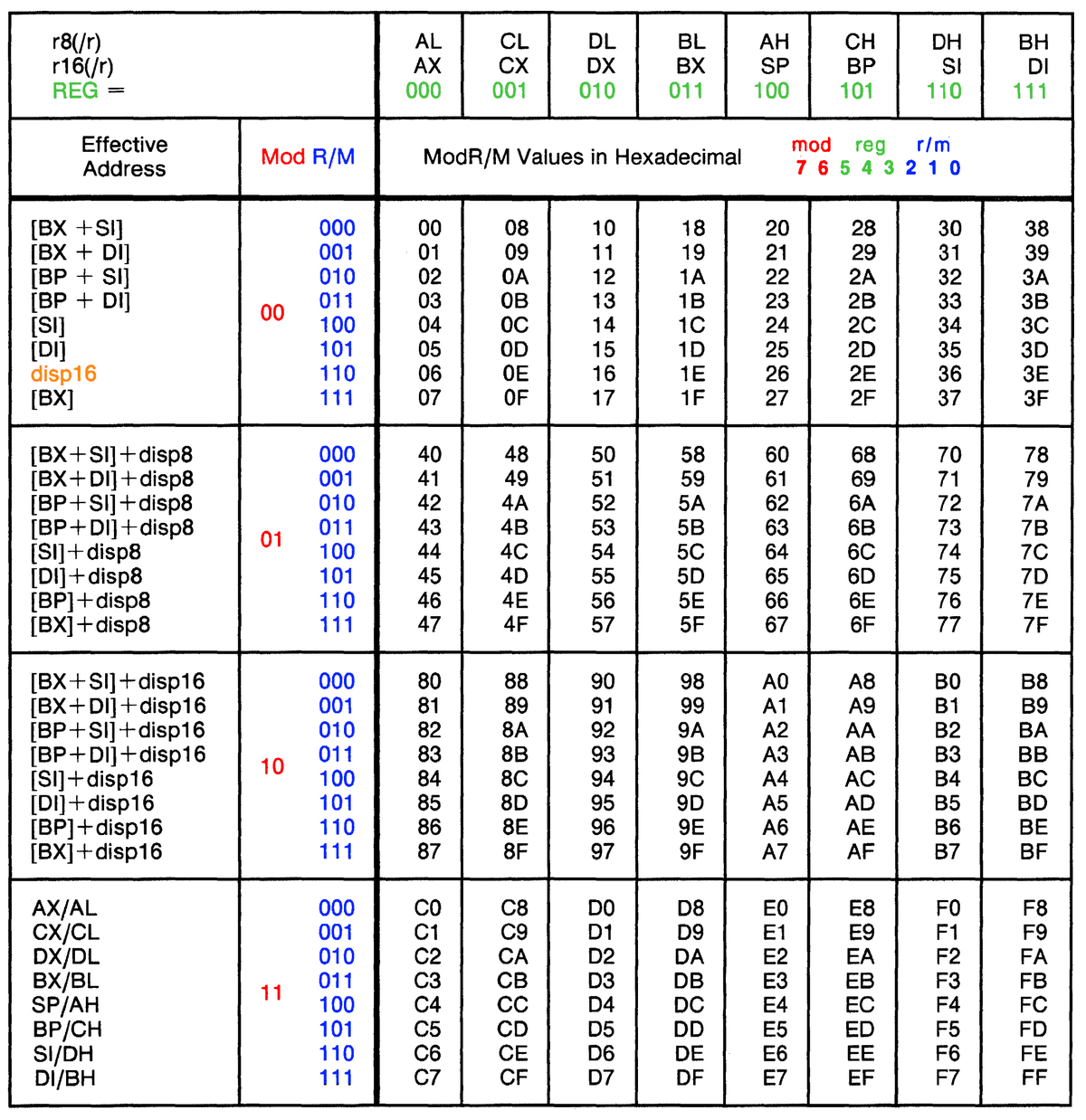
The table below shows the meaning of all 256 values for the ModR/M byte. The mod bits are colored red, the reg bits green, and the r/m bits blue. Note the special case "disp16" to support a 16-bit fixed address.

The ModR/M values. Note that this table would be trivial if it used octal rather than hexadecimal. Based on Table 6-13 in the ASM386 Assembly Language Reference.

The ModR/M values. Note that this table would be trivial if it used octal rather than hexadecimal. Based on Table 6-13 in the ASM386 Assembly Language Reference.

The register combinations for memory accesses may seem random but they were designed to support the needs of high-level languages, such as arrays and data structures. The idea is to add a base register, an index register, and/or a fixed displacement to determine the address.6 The base register can indicate the start of an array, the index register holds the offset in the array, and the displacement provides the offset of a field in the array entry. The base register is BX for data or BP for information on the stack. The index registers are SI (Source Index) and DI (Destination Index).7

Some addressing features are handled by the opcode, not the ModR/M byte. For instance, the ModR/M byte doesn't distinguish between ADD AX,[SI] and ADD [SI],AX. Instead, the two variants are distinguished by bit 1 of the instruction, the D or "direction" bit.8 Moreover, many instructions have one opcode that operates on words and another that operates on bytes, distinguished by bit 0 of the opcode, the W or word bit.

The D and W bits are an example of orthogonality in the 8086 instruction set, allowing features to be combined in various combinations. For instance, the addressing modes combine 8 types of offset computation with three sizes of displacements and 8 target registers. Arithmetic instructions combine these addressing modes with eight ALU operations, each of which can act on a byte or a word, with two possible memory directions. All of these combinations are implemented with one block of microcode, implementing a large instruction set with a small amount of microcode. (The orthogonality of the 8086 shouldn't be overstated, though; it has many special cases and things that don't quite fit.)

An overview of 8086 microcode

Most people think of machine instructions as the basic steps that a computer performs. However, many processors (including the 8086) have another layer of software underneath: microcode. With microcode, instead of building the control circuitry from complex logic gates, the control logic is largely replaced with code. To execute a machine instruction, the computer internally executes several simpler micro-instructions, specified by the microcode.

The 8086 uses a hybrid approach: although it uses microcode, much of the instruction functionality is implemented with gate logic. This approach removed duplication from the microcode and kept the microcode small enough for 1978 technology. In a sense, the microcode is parameterized. For instance, the microcode can specify a generic Arithmetic/Logic Unit (ALU) operation and a generic register. The gate logic examines the instruction to determine which specific operation to perform and the appropriate register.

A micro-instruction in the 8086 is encoded into 21 bits as shown below. Every micro-instruction has a move from a source register to a destination register, each specified with 5 bits. The meaning of the remaining bits depends on the type field. A "short jump" is a conditional jump within the current block of 16 micro-instructions. An ALU operation sets up the arithmetic-logic unit to perform an operation. Bookkeeping operations are anything from flushing the prefetch queue to ending the current instruction. A memory operation triggers a bus cycle to read or write memory. A "long jump" is a conditional jump to any of 16 fixed microcode locations (specified in an external table called the Translation ROM). Finally, a "long call" is a conditional subroutine call to one of 16 locations. For more about 8086 microcode, see my microcode blog post.

The encoding of a micro-instruction into 21 bits. Based on NEC v. Intel: Will Hardware Be Drawn into the Black Hole of Copyright?

The encoding of a micro-instruction into 21 bits. Based on NEC v. Intel: Will Hardware Be Drawn into the Black Hole of Copyright?

Some examples of microcode for addressing

In this section, I'll take a close look at a few addressing modes and how they are implemented in microcode. In the next section, I'll summarize all the microcode for addressing modes.

A register-register operation

Let's start by looking at a register-to-register instruction, before we get into the complications of memory accesses: ADD BX,AX which adds AX to BX, storing the result in BX. This instruction has the opcode value 01 and ModR/M value C3 (hex).

Before the microcode starts, the hardware performs some decoding of the opcode. The Group Decode ROM (below) classifies an instruction into multiple categories: this instruction contains a D bit, a W bit, and an ALU operation, and has a ModR/M byte. Fields from the opcode and ModR/M bytes are extracted and stored in various internal registers. The ALU operation type (ADD) is stored in the ALU opr register. From the ModR/M byte, the reg register code (AX) is stored in the N register, and the r/m register code (BX) is stored in the M register. (The M and N registers are internal registers that are invisible to the programmer; each holds a 5-bit register code that specifies a register.9)

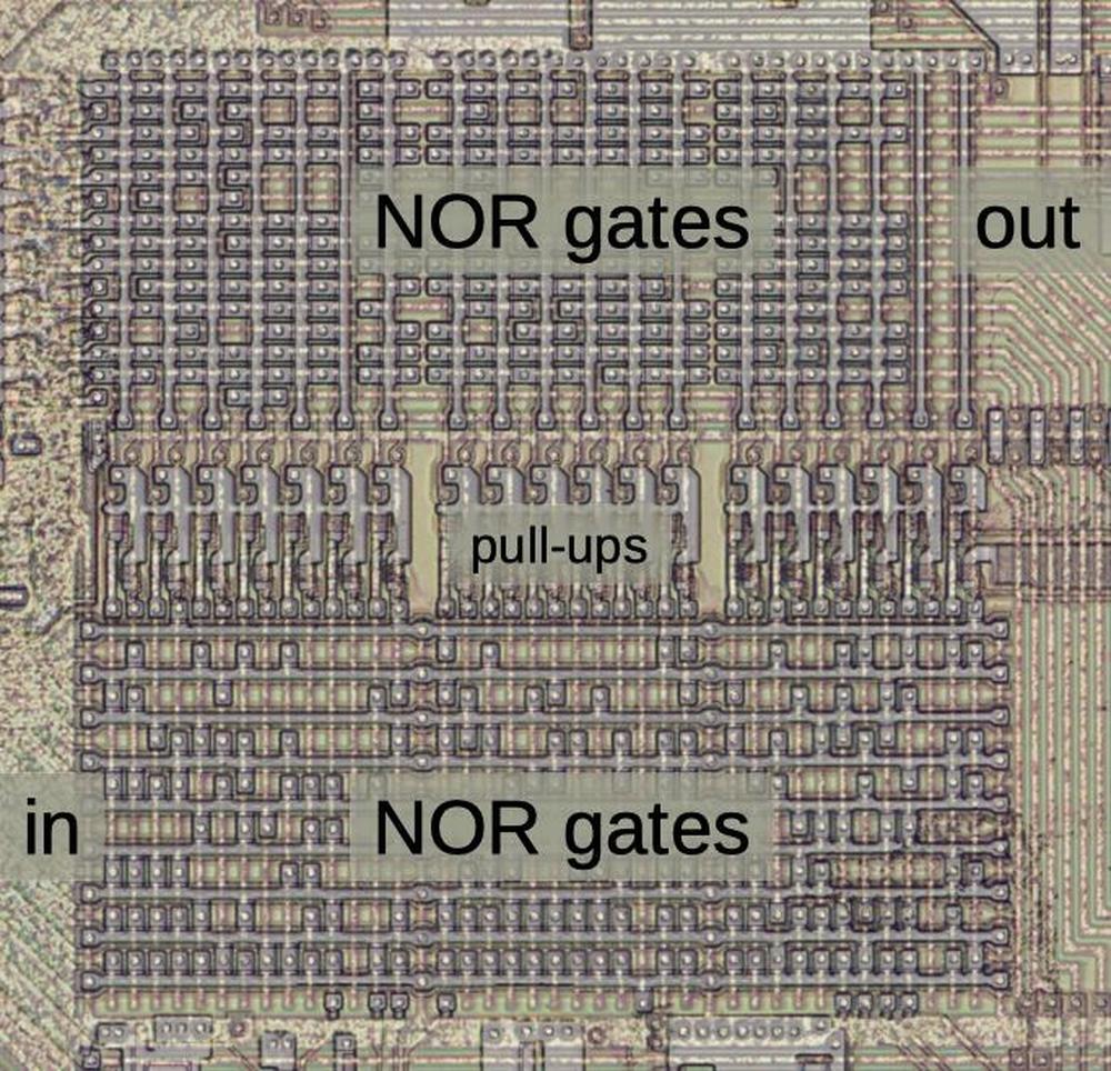
This diagram shows the Group Decode ROM. The Group Decode ROM is more of a PLA (programmable logic array) with two layers of NOR gates. Its input lines are at the lower left and its outputs are at the upper right.

This diagram shows the Group Decode ROM. The Group Decode ROM is more of a PLA (programmable logic array) with two layers of NOR gates. Its input lines are at the lower left and its outputs are at the upper right.

Once the preliminary decoding is done, the microcode below for this ALU instruction is executed.10 (There are three micro-instructions, so the instruction takes three clock cycles.) Each micro-instruction contains a move and an action. First, the register specified by M (i.e. BX) is moved to the ALU's temporary A register (tmpA). Meanwhile, the ALU is configured to perform the appropriate operation on tmpA; XI indicates that the ALU operation is specified by the instruction bits, i.e. ADD).

The second instruction moves the register specified by N (i.e. AX) to the ALU's tmpB register. The action NX indicates that this is the next-to-last micro-instruction so the microcode engine can start processing the next machine instruction. The last micro-instruction stores the ALU's result (Σ) in the register indicated by M (i.e. BX). The status flags are updated because of the F. WB,RNI (Run Next Instruction) indicates that this is the end and the microcode engine can process the next machine instruction. The WB prefix would skip the actions if a memory writeback were pending (which is not the case).

  move       action
M → tmpA     XI tmpA   ALU rm↔r: BX to tmpA
N → tmpB     WB,NX      AX to tmpB
Σ → M        WB,RNI F   result to BX, run next instruction.

This microcode packs a lot into three micro-instructions. Note that it is very generic: the microcode doesn't know what ALU operation is being performed or which registers are being used. Instead, the microcode deals with abstract registers and operations, while the hardware fills in the details using bits from the instructions. The same microcode is used for eight different ALU operations. And as we'll see, it supports multiple addressing modes.

Using memory as the destination

Memory operations on the 8086 involve both microcode and hardware. A memory operation uses two internal registers: IND (Indirect) holds the memory address, while OPR (Operand) holds the word that is read or written. A typical memory micro-instruction is R DS,P0, which starts a read from the Data Segment with a "Plus 0" on the IND register afterward. The Bus Interface Unit carries out this operation by adding the segment register to compute the physical address, and then running the memory bus cycles.

With that background, let's look at the instruction ADD [SI],AX, which adds AX to the memory location indexed by SI. As before, the hardware performs some analysis of the instruction (hex 01 04). In the ModR/M byte, mod=00 (memory, no displacement), reg=000 (AX), and R/M=100 ([SI]). The N register is loaded with the code for AX as before. The M register, however, is loaded with OPR (the memory data register) since the Group Decode ROM determines that the instruction has a memory addressing mode.

The microcode below starts in an effective address microcode subroutine for the [SI] mode. The first line of the microcode subroutine computes the effective address simply by loading the tmpA register with SI. It jumps to the micro-routine EAOFFSET which ends up at EALOAD (for reasons that will be described below), which loads the value from memory. Specifically, EALOAD puts the address in IND, reads the value from memory, puts the value into tmpB, and returns from the subroutine.

SI → tmpA   JMP EAOFFSET [SI]: put SI in tmpA
tmpA → IND  R DS,P0      EALOAD: read memory
OPR → tmpB  RTN  
M → tmpA    XI tmpA      ALU rm↔r: OPR to tmpA
N → tmpB    WB,NX         AX to tmpB
Σ → M       WB,RNI F      result to BX, run next instruction.
            W DS,P0 RNI   writes result to memory

Microcode execution continues with the ALU rm↔r routine described above, but with a few differences. The M register indicates OPR, so the value read from memory is put into tmpA. As before, the N register specifies AX, so that register is put into tmpB. In this case, the WB,NX determines that the result will be written back to memory so it skips the NXT operation. The ALU's result (Σ) is stored in OPR as directed by M. The WB,RNI is skipped so microcode execution continues. The W DS,P0 micro-instruction writes the result (in OPR) to the memory address in IND. At this point, RNI terminates the microcode sequence.

A lot is going on here to add two numbers! The main point is that the same microcode runs as in the register case, but the results are different due to the M register and the conditional WB code. By running different subroutines, different effective address computations can be performed.

Using memory as the source

Now let's look at how the microcode uses memory as a source, as in the instruction ADD AX,[SI]. This instruction (hex 03 04) has the same ModR/M byte as before, so the N register holds AX and the M register holds OPR. However, because the opcode has the D bit set, the M and N registers are swapped when accessed. Thus, when the microcode uses M, it gets the value AX from N, and vice versa. (Yes, this is confusing.)

The microcode starts the same as the previous example, reading [SI] into tmpB and returning to the ALU code. However, since the meaning of M and N are reversed, the AX value goes into tmpA while the memory value goes into tmpB. (This switch doesn't matter for addition, but would matter for subtraction.) An important difference is that there is no writeback to memory, so WB,NX starts processing the next machine instruction. In the last micro-instruction, the result is written to M, indicating the AX register. Finally, WB,RNI runs the next machine instruction.

SI → tmpA   JMP EAOFFSET [SI]: put SI in tmpA
tmpA → IND  R DS,P0      EALOAD: read memory
OPR → tmpB  RTN  
M → tmpA    XI tmpA      ALU rm↔r: AX to tmpA
N → tmpB    WB,NX         OPR to tmpB
Σ → M       WB,RNI F      result to AX, run next instruction.

The main point is that the same microcode handles memory as a source and a destination, simply by setting the D bit. First, the D bit reverses the operands by swapping M and N. Second, the WB conditionals prevent the writeback to memory that happened in the previous case.

Using a displacement

The memory addressing modes optionally support a signed displacement of one or two bytes. Let's look at the instruction ADD AX,[SI+0x1234]. In hex, this instruction is 03 84 34 12, where the last two bytes are the displacement, reversed because the 8086 uses little-endian numbers. The mod bits are 10, indicating a 16-bit displacement, but the other bits are the same as in the previous example.

Microcode execution again starts with the [SI] subroutine. However, the jump to EAOFFSET goes to [i] this time, to handle the displacement offset. (I'll explain how, shortly.) This code loads the offset as two bytes from the instruction prefetch queue (Q) into the tmpB register. It adds the offset to the previous address in tmpA and puts the sum Σ in tmpA, computing the effective address. Then it jumps to EAFINISH (EALOAD). From there, the code continues as earlier, reading an argument from memory and computing the sum.

SI → tmpA   JMP EAOFFSET [SI]: put SI in tmpA
Q → tmpBL   JMPS MOD1 12 [i]: load from queue, conditional jump
Q → tmpBH     
Σ → tmpA    JMP EAFINISH 12:
tmpA → IND  R DS,P0      EALOAD: read memory
OPR → tmpB  RTN  
M → tmpA    XI tmpA      ALU rm↔r: AX to tmpA
N → tmpB    WB,NX         OPR to tmpB
Σ → M       WB,RNI F      result to AX, run next instruction.

For the one-byte displacement case, the conditional MOD1 will jump over the fetch of the second displacement byte. When the first byte is loaded into the low byte of tmpB, it was sign-extended into the high byte.14 Thus, the one-byte displacement case uses the same microcode but ends up with a sign-extended 1-byte displacement in tmpB.

The Translation ROM

Now let's take a closer look at the jumps to EAOFFSET, EAFINISH, and the effective address subroutines, which use something called the Translation ROM. The Translation ROM converts the 5-bit jump tag in a micro-instruction into a 13-bit microcode address. It also provides the addresses of the effective address subroutines. As will be seen below, there are some complications.11

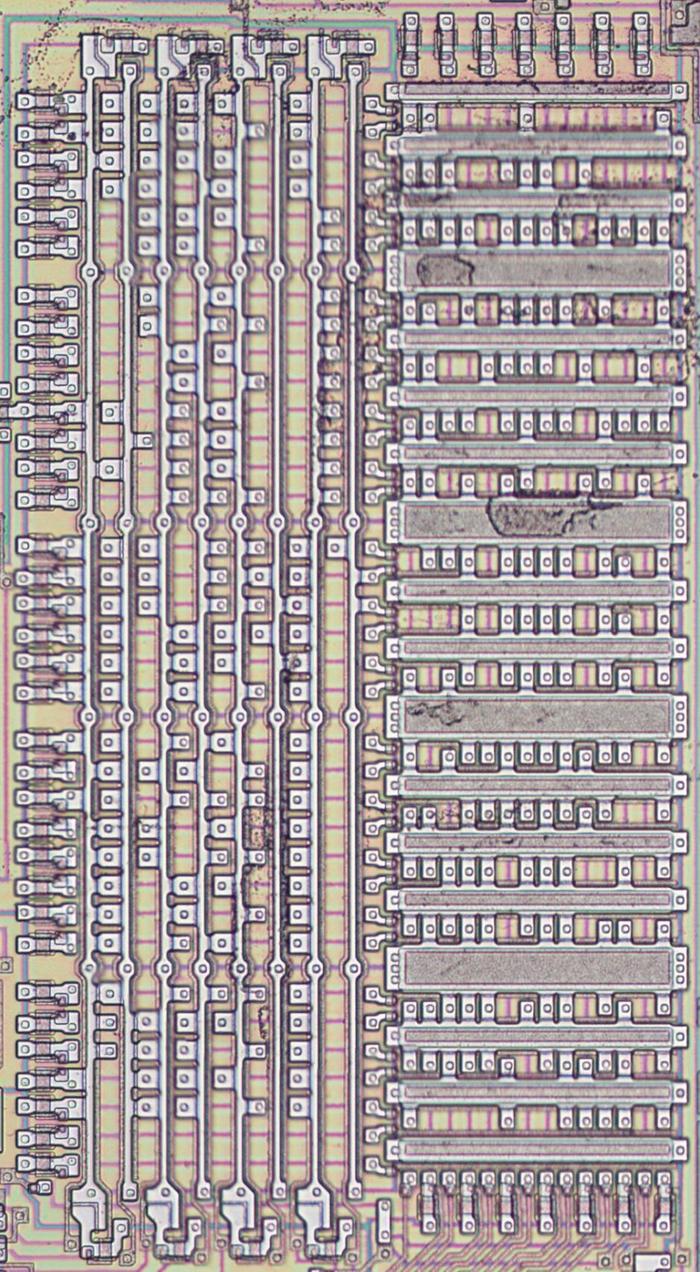
The Translation ROM as it appears on the die. The metal layer has been removed to expose the silicon and polysilicon underneath. The left half decodes the inputs to select a row. The right half outputs the corresponding microcode address.

The Translation ROM as it appears on the die. The metal layer has been removed to expose the silicon and polysilicon underneath. The left half decodes the inputs to select a row. The right half outputs the corresponding microcode address.

The effective address micro-routines

Register calculations

The Translation ROM has an entry for the addressing mode calculations such as [SI] and [BP+DI], generally indicated by the r/m bits, the three low bits of the ModR/M byte. Each routine computes the effective address and puts it into the ALU's temporary A register and jumps to EAOFFSET, which adds any displacement offset. The microcode below shows the four simplest effective address calculations, which just load the appropriate register into tmpA.

SI → tmpA   JMP EAOFFSET   [SI]: load SI into tmpA
DI → tmpA   JMP EAOFFSET   [DI]: load SI into tmpA
BP → tmpA   JMP EAOFFSET   [BP]: load BP into tmpA
BX → tmpA   JMP EAOFFSET   [BX]: load BX into tmpA

For the cases below, an addition is required, so the registers are loaded into the ALU's temporary A and temporary B registers. The effective address is the sum (indicated by Σ), which is moved to temporary A.12 These routines are carefully arranged in memory so [BX+DI] and [BP+SI] each execute one micro-instruction and then jump into the middle of the other routines, saving code.13

BX → tmpA         [BX+SI]: get regs
SI → tmpB         1:
Σ → tmpA   JMP EAOFFSET  

BP → tmpA         [BP+DI]: get regs
DI → tmpB         4:
Σ → tmpA   JMP EAOFFSET  

BX → tmpA  JMPS 4 [BX+DI]: short jump to 4
BP → tmpA  JMPS 1 [BP+SI]: short jump to 1

The EAOFFSET and EAFINISH targets

After computing the register portion of the effective address, the routines above jump to EAOFFSET, but this is not a fixed target. Instead, the Translation ROM selects one of three target microcode addresses based on the instruction and the ModR/M byte:
If there's a displacement, the microcode jumps to [i] to add the displacement value.
If there is no displacement but a memory read, the microcode otherwise jumps to EALOAD to load the memory contents.
If there is no displacement and no memory read should take place, the microcode jumps to EADONE.
In other words, the microcode jump is a three-way branch that is implemented by the Translation ROM and is transparent to the microcode.

For a displacement, the [i] immediate code below loads a 1-byte or 2-byte displacement into the tmpB register and adds it to the tmpA register, as described earlier. At the end of a displacement calculation, the microcode jumps to the EAFINISH tag, which is another branching target. Based on the instruction, the Translation ROM selects one of two microcode targets: EALOAD to load from memory, or EADONE to skip the load.

Q → tmpBL   JMPS MOD1 12 [i]: get byte(s)
Q → tmpBH         
Σ → tmpA    JMP EAFINISH 12: add displacement

The EALOAD microcode below reads the value from memory, using the effective address in tmpA. It puts the result in tmpB. The RTN micro-instruction returns to the microcode that implements the original machine instruction.

tmpA → IND  R DS,P0   EALOAD: read from tmpA address
OPR → tmpB  RTN        store result in tmpB, return

The EADONE routine puts the effective address in IND, but it doesn't read from the memory location. This supports machine instructions such as MOV (some moves) and LEA (Load Effective Address) that don't read from memory

tmpA → IND  RTN   EADONE: store effective address in IND

To summarize, the microcode runs different subroutines and different paths, depending on the addressing mode, executing the appropriate code. The Translation ROM selects the appropriate control flow path.

Special cases

There are a couple of special cases in addressing that I will discuss in this section.

Supporting a fixed address

It is common to access a fixed memory address, but the standard addressing modes use a base or index register. The 8086 replaces the mode of [BP] with no displacement with 16-bit fixed addressing. In other words, a ModR/M byte with the pattern 00xxx110 is treated specially. (This special case is the orange disp16 line in the ModR/M table earlier.) This is implemented in the Translation ROM which has additional rows to detect this pattern and execute the immediate word [iw] microcode below instead. This microcode fetches a word from the instruction prefetch queue (Q) into the tmpA register, a byte at a time. It jumps to EAFINISH instead of EAOFFSET because it doesn't make sense to add another displacement.

Q → tmpAL          [iw]: get bytes
Q → tmpAH  JMP EAFINISH  

Selecting the segment

Memory accesses in the 8086 are relative to one of the 64-kilobyte segments: Data Segment, Code Segment, Stack Segment, or Extra Segment. Most addressing modes use the Data Segment by default. However, addressing modes that use the BP register use the Stack Segment by default. This is a sensible choice since the BP (Base Pointer) register is intended for accessing values on the stack.

This special case is implemented in the Translation ROM. It has an extra output bit that indicates that the addressing mode should use the Stack Segment. Since the Translation ROM is already decoding the addressing mode to select the right microcode routine, adding one more output bit is straightforward. This bit goes to the segment register selection circuitry, changing the default segment. This circuitry also handles prefixes that change the segment. Thus, segment register selection is handled in hardware without any action by the microcode.

Conclusions

I hope you have enjoyed this tour through the depths of 8086 microcode. The effective address calculation in the 8086 uses a combination of microcode and logic circuitry to implement a variety of addressing methods. Special cases make the addressing modes more useful, but make the circuitry more complicated. This shows the CISC (Complex Instruction Set Computer) philosophy of x86, making the instructions complicated but highly functional. In contrast, the RISC (Reduced Instruction Set Computer) philosophy takes the opposite approach, making the instructions simpler but allowing the processor to run faster. RISC vs. CISC was a big debate of the 1980s, but isn't as relevant nowadays.

People often ask if microcode could be updated on the 8086. Microcode was hardcoded into the ROM, so it could not be changed. This became a big problem for Intel with the famous Pentium floating-point division bug. The Pentium chip turned out to have a bug that resulted in rare but serious errors when dividing. Intel recalled the defective processors in 1994 and replaced them at a cost of $475 million. Starting with the Pentium Pro (1995), microcode could be patched at boot time, a useful feature that persists in modern CPUs.

I've written multiple posts on the 8086 so far and plan to continue reverse-engineering the 8086 die so follow me on Twitter @kenshirriff or RSS for updates. I've also started experimenting with Mastodon recently as @oldbytes.space@kenshirriff.

Notes and references

  1. There are additional addressing modes that don't use a ModR/M byte. For instance, immediate instructions use a constant in the instruction. For instance ADD AX,42 adds 42 to the AX register. Other instructions implicitly define the addressing mode. I'm ignoring these instructions for now. 

  2. The 8086 supports more addressing modes than the ModR/M byte provides, by using separate opcodes. For instance, arithmetic instructions can take an "immediate" value, an 8- or 16-bit value specified as part of the instruction. Other instructions operate on specific registers rather than memory or access memory through the stack. For this blog post, I'm focusing on the ModR/M modes and ignoring the other instructions. Also, although I'm discussing the 8086, this blog post applies to the Intel 8088 processor as well. The 8088 has an 8-bit bus, a smaller prefetch queue, and some minor internal changes, but for this post you can consider them to be the same. 

  3. My assembly code examples are based on Intel ASM86 assembly syntax. There's a completely different format of x86 assembly language known as AT&T syntax. Confusingly, it reverses the source and destination. For example, in AT&T syntax, addw %bx, %cx% stores the result in CX. AT&T syntax is widely used, for instance in Linux code. The AT&T syntax is based on earlier PDP-11 assembly code

  4. The term "effective address" dates back to the 1950s, when computers moved beyond fixed memory addresses and started using index registers. The earliest uses that I could find are from 1955 for the IBM 650 data processing machine and the IBM 704 mainframe. The "Load Effective Address" instruction, which provides the effective address as a value instead of performing the memory access, was perhaps introduced in the IBM System/360 (1964) under the name "Load Address". It has been a part of many subsequent processors including the 8086. 

  5. Note that the ModR/M byte has the bits grouped in threes (as do many instructions). This is due to the octal heritage of the 8086, dating back through the 8080 and the 8008 to the Datapoint 2200 (which used TTL chips to decode groups of three bits). Although the 8086 instruction set is invariably described in hexadecimal, it makes much more sense when viewed in octal. See x86 is an octal machine for details. 

  6. The 8086's addressing schemes are reminiscent of the IBM System/360 (1964). In particular, System/360 had a "RX" instruction format that accessed memory through a base register plus an index register plus a displacement, using another register for the other argument. This is very similar to the 8086's base + index + displacement method. The System/360's "RR" (register-register) instruction format accessed two registers, much like the register mode of the ModR/M byte. The details are very different, though, between the two systems. See the IBM System/360 Principles of Operation for more details. 

  7. The motivation behind the ModR/M options is discussed in The 8086/8088 Primer by 8086 designer Steve Morse, pages 23-33. 

  8. The D bit is usually called the register direction bit, but the designer of the 8086 instruction set calls it the destination field; see The 8086/8088 Primer, Steve Morse, page 28. To summarize:
    If the bit is 0, the result is stored into the location indicated by the mod and r/m fields while the register specified by reg is the source.
    If the bit is 1, the result is stored into the register indicated by the reg field.

    For the W word bit, 0 indicates a byte operation and 1 indicates a word operation.

    One curious side-effect of the D bit is that an instruction like ADD AX,BX can be implemented in two ways since both arguments are registers. The reg field can specify AX while the r/m field specifies BX or vice versa, depending on the D bit. Different 8086 assemblers can be "fingerprinted" based on their decisions in these ambiguous cases. 

  9. The M and N registers hold a 5-bit code. This code indicates a 16-bit register (e.g. AX or IND), an 8-bit register (e.g. AL), or a special value (e.g. Σ, the ALU result; ZEROS, all zero bits; or F, the flags). The 3-bit register specification is mapped onto the 5-bit code depending on whether the W bit is set (byte or word register), or if the operation is specifying a segment register. 

  10. The microcode listings are based on Andrew Jenner's disassembly. I have made some modifications to (hopefully) make it easier to understand. 

  11. You can also view the Translation ROM as a PLA (Programmable Logic Array) constructed from two layers of NOR gates. The conditional entries make it seem more like a PLA than a ROM. Technically, it can be considered a ROM since a single row is active at a time. I'm using the name "Translation ROM" because that's what Intel calls it in the patents. 

  12. Normally, an ALU operation requires a micro-instruction to specify the desired ALU operation and temporary register. For the address addition, the ALU operation is not explicitly specified because it uses the ALU's default, of adding tmpA and tmpB. The ALU is reset to this default at the beginning of each machine instruction. 

  13. A microcode jump takes an extra clock cycle for the microcode address register to get updated. This is why, for instance, [BP+DI] takes 7 clock cycles but [BX+DI] takes 8 clock cycles. Thus, the 8086 implementers took the tradeoff of slowing down some addressing modes by a clock cycle in order to save a few micro-instructions in the small microcode ROM.

    This table shows the clock cycles required for effective address calculations. From MCS-86 Assembly Language Reference Guide.

    This table shows the clock cycles required for effective address calculations. From MCS-86 Assembly Language Reference Guide.


  14. A one-byte signed number can be sign-extended into a two-byte signed number. This is done by copying the top bit (the sign) from the low byte and filling the top byte with that bit. For example, 0x64 is sign-extended to 0x0064 (+100), while 0x9c is sign-extended to 0xff9c (-100).