Showing posts sorted by date for query ibm 1401. Sort by relevance Show all posts

How the 8086 processor determines the length of an instruction

The Intel 8086 processor (1978) has a complicated instruction set with instructions ranging from one to six bytes long. This raises the question of how the processor knows the length of an instruction.1 The answer is that the 8086 uses an interesting combination of lookup ROMs and microcode to determine how many bytes to use for an instruction. In brief, the ROMs perform enough decoding to figure out if it needs one byte or two. After that, the microcode simply consumes instruction bytes as it needs them. Thus, nothing in the chip explicitly "knows" the length of an instruction. This blog post describes this process in more detail.

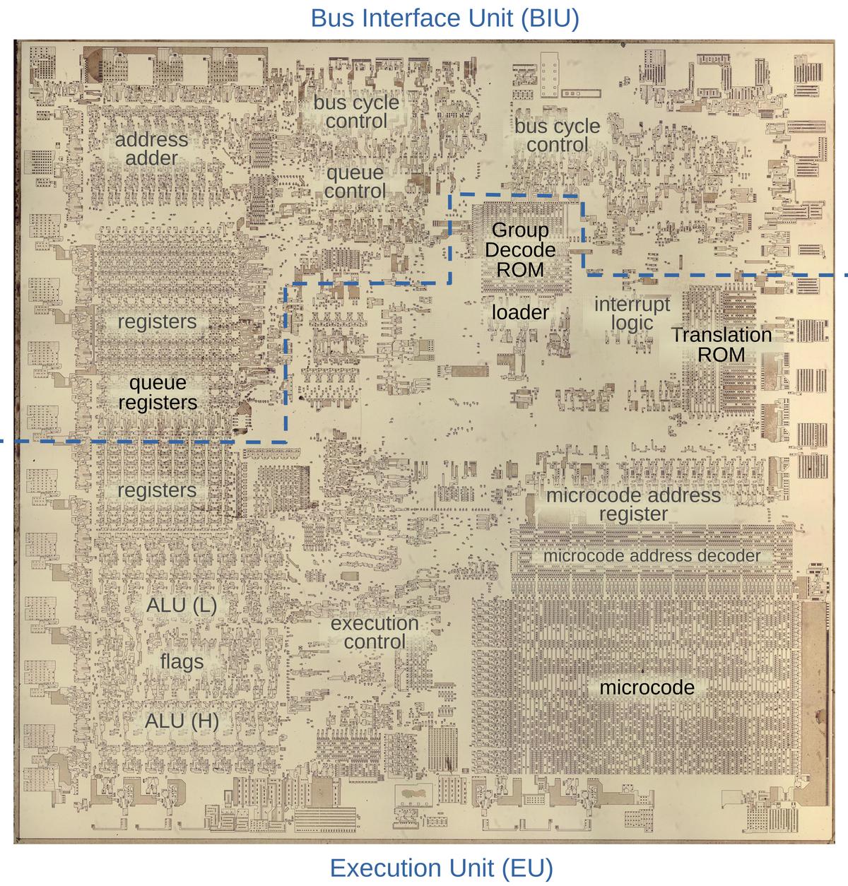
The die photo below shows the chip under a microscope. I've labeled the key functional blocks; the ones that are important to this post are darker. Architecturally, the chip is partitioned into a Bus Interface Unit (BIU) at the top and an Execution Unit (EU) below. The BIU handles bus and memory activity as well as instruction prefetching, while the Execution Unit (EU) executes the instructions.

The 8086 die under a microscope, with main functional blocks labeled. This photo shows the chip with the metal and polysilicon removed, revealing the silicon underneath. Click on this image (or any other) for a larger version.

The 8086 die under a microscope, with main functional blocks labeled. This photo shows the chip with the metal and polysilicon removed, revealing the silicon underneath. Click on this image (or any other) for a larger version.

The prefetch queue, the loader, and the microcode

The 8086 uses a 6-byte instruction prefetch queue to hold instructions, and this queue will play an important role in this discussion.3 Earlier microprocessors read instructions from memory as they were needed, which could cause the CPU to wait on memory. The 8086, instead, read instructions from memory before they were needed, storing them in the instruction prefetch queue. (You can think of this as a primitive instruction cache.) To execute an instruction, the 8086 took bytes out of the queue one at a time. If the queue ran empty, the processor waited until more instruction bytes were fetched from memory into the queue.

A circuit called the loader handles the interaction between the prefetch queue and instruction execution. The loader is a small state machine that provides control signals to the rest of the execution circuitry. The loader gets the first byte of an instruction from the prefetch queue and issues a signal FC (First Clock) that starts execution of the instruction.

At this point, the Group Decode ROM performs the first stage of instruction decoding, classifying the instruction into various categories based on the opcode byte. Most of the 8086's instructions are implemented in microcode. However, a few instructions are so simple that they are implemented with logic circuits. For example, the CLC (Clear Carry) instruction clears the carry flag directly. The Group Decode ROM categorizes these instructions as 1BL (one-byte, implemented in logic). The loader responds by issuing an SC (Second Clock) signal to wrap up execution and start the next instruction. Thus, these simple instructions take two clock cycles.

The 8086 has various prefix bytes that can be put in front of an instruction to change its behavior. For instance, a segment prefix changes the memory segment that the instruction uses. A LOCK prefix locks the bus during the next instruction. The Group Decode ROM detects a prefix and outputs a prefix signal. This causes the prefix to be handled in logic, rather than microcode, similar to the 1BL instructions. Thus, a prefix also takes one byte and two clock cycles.

The remaining instructions are handled by microcode.2 Let's start with a one-byte instruction such as INC AX, which increments the AX register. As before, the loader gets the instruction byte from the prefix queue. The Group Decode ROM determines that this instruction is implemented in microcode and can start after one byte, so the microcode engine starts running. The microcode below handles the increment and decrement instructions. It moves the appropriate register, indicated by M to the ALU's temporary B register. It puts the incremented or decremented result (Σ) back into the register (M). RNI tells the loader to run the next instruction. With two micro-instruction, this instruction takes two clock cycles.

M → tmpB        XI tmpB, NX INC/DEC: get value from M, set up ALU
Σ → M           WB,RNI F     put result in M, run next instruction

But what happens with an instruction that is more than one byte long, such as adding an immediate value to a register? Let's look at ADD AX,1234, which adds 1234 to the AX register. As before, the loader reads one byte and then the microcode engine starts running. At this point, the 8086 doesn't "realize" that this is a 3-byte instruction. The first line of the microcode below gets one byte of the immediate operand: Q→tmpBL loads a byte from the instruction prefetch queue into the low byte of the temporary B register. Similarly, the second line loads the second byte. The next line puts the register value (M) in tmpA. The last line puts the sum back into the register and runs the next instruction. Since this instruction takes two bytes from the prefetch queue, it is three bytes long in total. But nothing explicitly indicates this instruction is three bytes long.

Q → tmpBL       JMPS L8 2  alu A,i: get byte from queue
Q → tmpBH                   get byte from queue
M → tmpA        XI tmpA, NX get value from M, set up ALU
Σ → M           WB,RNI F    put result in M, run next instruction

You can also add a one-byte immediate value to a register, such as ADD AL,12. This uses the same microcode above. However, in the first line, JMPS L8 is a conditional jump that skips the second micro-instruction if the data length is 8 bits. Thus, the microcode only consumes one byte from the prefetch queue, making the instruction two bytes long. In other words, what makes this instruction two bytes instead of three is the bit in the opcode which triggers the conditional jump in the microcode.

The 8086 has another class of instructions, those with a ModR/M byte following the opcode. The Group Decode ROM classifies these instructions as 2BR (two-byte ROM) indicating that the second byte must be fetched before processing by the microcode ROM. For these instructions, the loader fetches the second byte from the prefetch queue before triggering the SC (Second Clock signal) to start microcode execution.

The ModR/M byte indicates the addressing mode that the instruction should use, such as register-to-register or memory-to-register. The ModR/M can change the instruction length by specifying an address displacement of one or two bytes. A second ROM called the Translation ROM selects the appropriate microcode for the addressing mode (details). For example, if the addressing mode includes an address displacement, the microcode below is used:

Q → tmpBL   JMPS MOD1 12 [i]: get byte(s)
Q → tmpBH         
Σ → tmpA    BX EAFINISH 12: add displacement

This microcode fetches two displacement bytes from the prefetch queue (Q). However, if the ModR/M byte specifies a one-byte displacement, the MOD1 condition causes the microcode to jump over the second fetch. Thus, this microcode uses one or two additional instruction bytes depending on the value of the ModR/M byte.

To summarize, nothing in the 8086 "knows" how long an instruction is. The Group Decode ROM makes part of the decision, classifying instructions as a prefix, 1-byte logic, 2-byte ROM, or otherwise, causing the loader to fetch one or two bytes. The microcode then consumes instruction bytes as needed. In the end, the length of an 8086 instruction is determined by how many bytes are taken from the prefetch queue by the time it ends.

Some other systems

It's interesting to see how other processors deal with instruction length. For example, RISC processors (Reduced Instruction Set Computers) typically have fixed-length instructions. For instance, the ARM-1 processor used 32-bit instructions, making instruction decoding very simple.

Early microprocessors such as the MOS Technology 6502 (1975) didn't use microcode, but were controlled by state machines. The CPU fetches instruction bytes from memory as needed, as it moves through various execution states. Thus, as with the 8086, the length of an instruction wasn't explicit, but was how many bytes it used.

The IBM 1401 computer (1959) took a completely different approach with its variable-length words. Each character in memory had an associated "word mark" bit, which you can think of as a metadata bit. Each machine instruction consisted of a variable number of characters with a word mark on the first one. Thus, the processor could read instruction characters until it hit a word mark, which indicated the start of the next instruction. The word mark explicitly indicated to the processor how long each instruction was.

Perhaps the worst approach for variable-length instructions was the Intel iAPX 432 processor (1981), which had instructions with variable bit lengths, from 6 to 321 bits long. As a result, instructions weren't aligned on byte boundaries, making instruction decoding even more inconvenient. This was just one of the reasons that the iAPX 432 ended up overly complicated, years behind schedule, and a commercial failure.

The 8086's variable-length instructions led to the x86 architecture, with instructions from 1 to 15 bytes long. This is particularly inconvenient with modern superscalar processors that run multiple instructions in parallel. The problem is that the processor must break the instruction stream into individual instructions before they execute. The Intel P6 microarchitecture used in the Pentium Pro (1995) has instruction decoders to decode the instruction stream into micro-operations.4 It starts with an "instruction length block" that analyzes the first bytes of the instruction to determine how long it is. (This is not a straightforward task to perform rapidly on multiple instructions in parallel.) The "instruction steering block" uses this information to break the byte stream into instructions and steer instructions to the decoders.

The AMD K6 3D processor (1999) had predecode logic that associated 5 predecode bits with each instruction byte: three pointed to the start of the next instruction, one indicated the length depended on a D bit, and one indicated the presence of a ModR/M byte. This logic examined up to three bytes to make its decisions. Instructions were split apart and assigned to decoders based on the predecode bits. In some cases, the predecode logic gave up and flagged the instruction as "unsuccessfully predecoded", for instance an instruction longer than 7 bytes. These instructions were handled by a slower path.

Conclusions

The 8086 processor has instructions with a variety of lengths, but nothing in the processor explicitly determines the length. Instead, an instruction uses as many bytes as it needs. (That sounds sort of tautological, but I'm not sure how else to put it.) The Group Decode ROM makes an initial classification, the Translation ROM determines the addressing mode, and the microcode consumes bytes as needed.

While this approach gave the 8086 a flexible instruction set, it created a problem in the long run for the x86 architecture, requiring complicated logic to determine instruction length. One benefit of RISC-based processors such as the Apple M1 is that they have (mostly) constant instruction lengths, making instruction decoding faster and simpler.

I've written multiple posts on the 8086 so far and plan to continue reverse-engineering the 8086 die so follow me on Twitter @kenshirriff or RSS for updates. I've also started experimenting with Mastodon recently as @oldbytes.space@kenshirriff.

Notes and references

  1. I was inspired to investigate instruction length based on a Stack Overflow question

  2. I'll just give a brief overview of microcode here. Each micro-instruction is 21 bits long, as shown below. A micro-instruction specifies a move between a source register and destination register. It also has an action that depends on the micro-instruction type. For more details, see my post on the 8086 microcode pipeline.

    The encoding of a micro-instruction into 21 bits. Based on NEC v. Intel: Will Hardware Be Drawn into the Black Hole of Copyright?

    The encoding of a micro-instruction into 21 bits. Based on NEC v. Intel: Will Hardware Be Drawn into the Black Hole of Copyright?


  3. The 8088 processor, used in the original IBM PC, has a smaller 4-byte prefetch queue. The 8088 is almost the same as the 8086, except it has an 8-bit external bus instead of a 16-bit external bus. This makes memory accesses (including prefetches) slower, so a smaller prefetch queue works better. 

  4. The book Modern Processor Design discusses the P6 microarchitecture in detail. The book The Anatomy of a High-Performance Microprocessor discusses the AMD K5 3D processor in even more detail; see chapter 2. 

Understanding the x86's Decimal Adjust after Addition (DAA) instruction

I've been looking at the DAA machine instruction on x86 processors, a special instruction for binary-coded decimal arithmetic. Intel's manuals document each instruction in detail, but the DAA description doesn't make much sense. I ran an extensive assembly-language test of DAA on a real machine to determine exactly how the instruction behaves. In this blog post, I explain how the instruction works, in case anyone wants a better understanding.

The DAA instruction

The DAA (Decimal Adjust AL1 after Addition) instruction is designed for use with packed BCD (Binary-Coded Decimal) numbers. The idea behind BCD is to store decimal numbers in groups of four bits, with each group encoding a digit 0-9 in binary. You can fit two decimal digits in a byte; this format is called packed BCD. For instance, the decimal number 23 would be stored as hex 0x23 (which turns out to be decimal 35).

The 8086 doesn't implement BCD addition directly. Instead, you use regular binary addition and then DAA fixes the result. For instance, suppose you're adding decimal 23 and 45. In BCD these are 0x23 and 0x45 with the binary sum 0x68, so everything seems straightforward. But, there's a problem with carries. For instance, suppose you add decimal 26 and 45 in BCD. Now, 0x26 + 0x45 = 0x6b, which doesn't match the desired answer of 0x71. The problem is that a 4-bit value has a carry at 16, while a decimal digit has a carry at 10. The solution is to add a correction factor of the difference, 6, to get the correct BCD result: 0x6b + 6 = 0x71.

Thus, if a sum has a digit greater than 9, it needs to be corrected by adding 6. However, there's another problem. Consider adding decimal 28 and decimal 49 in BCD: 0x28 + 0x49 = 0x71. Although this looks like a valid BCD result, it is 6 short of the correct answer, 77, and needs a correction factor. The problem is the carry out of the low digit caused the value to wrap around. The solution is for the processor to track the carry out of the low digit, and add a correction if a carry happens. This flag is usually called a half-carry, although Intel calls it the Auxiliary Carry Flag.2

For a packed BCD value, a similar correction must be done for the upper digit. This is accomplished by the DAA (Decimal Adjust AL after Addition) instruction. Thus, to add a packed BCD value, you perform an ADD instruction followed by a DAA instruction.

Intel's explanation

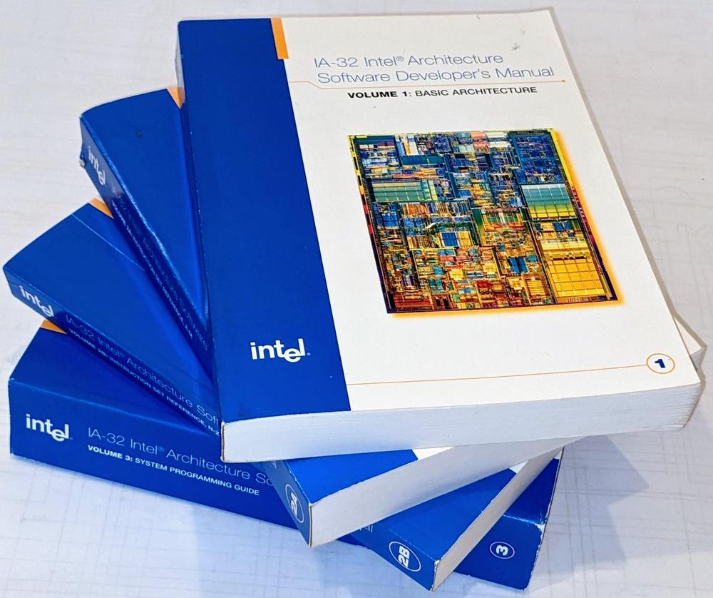
The Intel Software Developer's Manuals. These are from 2004, back when Intel would send out manuals on request.

The Intel Software Developer's Manuals. These are from 2004, back when Intel would send out manuals on request.

The Intel 64 and IA-32 Architectures Software Developer Manuals provide detailed pseudocode specifying exactly what each machine instruction does. However, in the case of DAA, the pseudocode is confusing and the description is ambiguous. To verify the operation of the DAA instruction on actual hardware, I wrote a short assembly program to perform DAA on all input values (0-255) and all four combinations of the carry and auxiliary flags.3 I tested the pseudocode against this test output. I determined that Intel's description is technically correct, but can be significantly simplified.

The manual gives the following pseudocode; my comments are in green.

IF 64-Bit Mode
  THEN
    #UD;  Undefined opcode in 64-bit mode
  ELSE
    old_AL := AL; AL holds input value
    old_CF := CF; CF is the carry flag
    CF := 0;
    IF (((AL AND 0FH) > 9) or AF = 1) AF is the auxiliary flag
      THEN
        AL := AL + 6;
        CF := old_CF or (Carry from AL := AL + 6); dead code
        AF := 1;
      ELSE
        AF := 0;
      FI;
    IF ((old_AL > 99H) or (old_CF = 1))
      THEN
        AL := AL + 60H;
        CF := 1;
      ELSE
        CF := 0;
    FI;
FI;

Removing the unnecessary code yields the version below, which makes it much clearer what is going on. The low digit is corrected if it exceeds 9 or if the auxiliary flag is set on entry. The high digit is corrected if it exceeds 9 or if the carry flag is set on entry.4 At completion, the auxiliary and carry flags are set if an adjustment happened to the corresponding digit.5 (Because these flags force a correction, the operation never clears them if they were set at entry.)

IF 64-Bit Mode
  THEN
    #UD;
  ELSE
    old_AL := AL;
    IF (((AL AND 0FH) > 9) or AF = 1)
      THEN
        AL := AL + 6;
        AF := 1;
      FI;
    IF ((old_AL > 99H) or CF = 1)
      THEN
        AL := AL + 60H;
        CF := 1;
    FI;
FI;

History of BCD

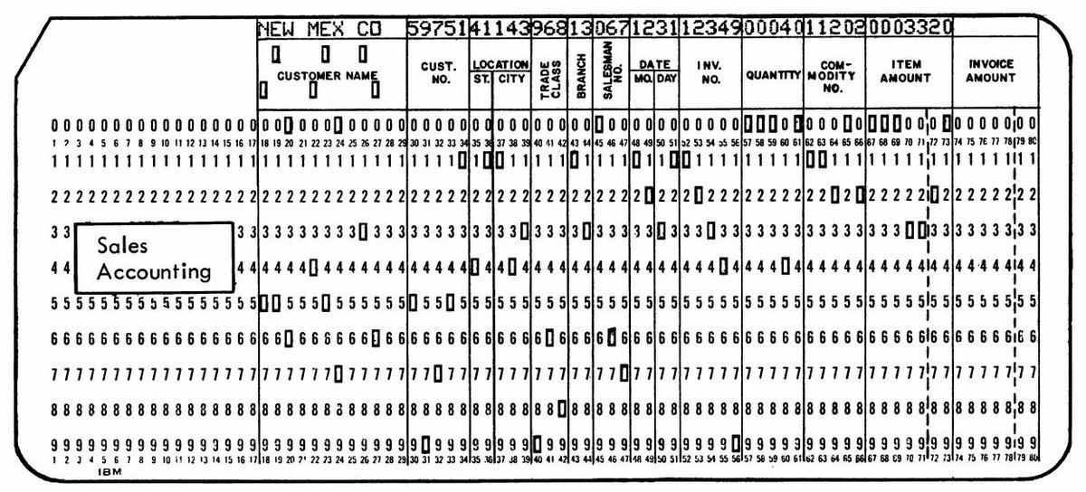
The use of binary-coded decimal may seem strange from the modern perspective, but it makes more sense looking at some history. In 1928, IBM introduced the 80-column punch card, which became very popular for business data processing. These cards store one decimal digit per column, with each digit indicated by a single hole in row 0 through 9.6 Even before digital computers, businesses could perform fairly complex operations on punch-card data using electromechanical equipment such as sorters and collators. Tabulators, programmed by wiring panels, performed arithmetic on punch cards using electromechanical counting wheels and printed business reports.

Example card, from IBM 29 Card Punch Reference Manual.

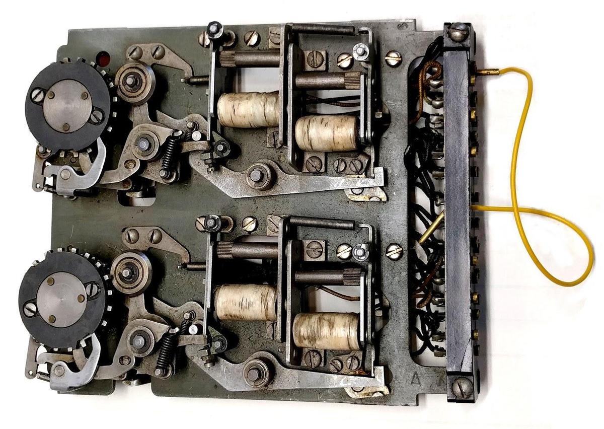
These calculations were performed in decimal. Decimal fields were read off punch cards, added with decimal counting wheels, and printed as decimal digits. Numbers were not represented in binary, or even binary-coded decimal. Instead, digits were represented by the position of the hole in the card, which controlled the timing of pulses inside the machinery. These pulses rotated counting wheels, which stored their totals as angular rotations, a bit like an odometer.

A counter unit from an IBM accounting machine (tabulator). The two wheels held two digits. The electromagnets (white) engaged and disengaged the clutch so the wheel would advance the desired number of positions.

A counter unit from an IBM accounting machine (tabulator). The two wheels held two digits. The electromagnets (white) engaged and disengaged the clutch so the wheel would advance the desired number of positions.

With the rise of electronic digital computers in the 1950s, you might expect binary to take over. Scientific computers used binary for their calculations, such as the IBM 701 (1952). However, business computers such as the IBM 702 (1955) and the IBM 1401 (1959) operated on decimal digits, typically stored as binary-coded decimal in 6-bit characters. Unlike the scientific computers, these business computers performed arithmetic operation in decimal.

The main advantage of decimal arithmetic was compatibility with decimal fields stored in punch cards. Second, decimal arithmetic avoided time-consuming conversions between binary and decimal, a benefit for applications that were primarily input and output rather than computation. Finally, decimal arithmetic avoided the rounding and truncation problems that can happen if you use floating-point numbers for accounting calculations.

The importance of decimal arithmetic to business can be seen in its influence on the COBOL programming language, very popular for business applications. A data field was specified with the PICTURE clause, which specified exactly how many decimal digits each field contained. For instance PICTURE S999V99 specified a five-digit number (five 9's) with a sign (S) and implied decimal point (V). (Binary fields were an optional feature.)

In 1964, IBM introduced the System/360 line of computers, designed for both scientific and business use, the whole 360° of applications. The System/360 architecture was based on 32-bit binary words. But to support business applications, it also provided decimal data structures. Packed decimal provided variable-length decimal fields by putting two binary-coded decimal digits per byte. A special set of arithmetic instructions supported addition, subtraction, multiplication, and division of decimal values.

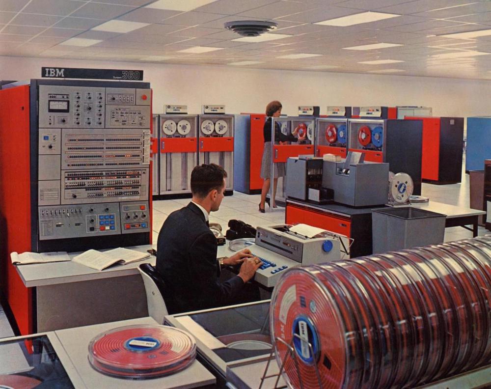
The System/360 Model 50 in a datacenter. The console and processor are at the left. An IBM 1442 card reader/punch is behind the IBM 1052 printer-keyboard that the operator is using. At the back, another operator is loading a tape onto an IBM 2401 tape drive. Photo from IBM.

The System/360 Model 50 in a datacenter. The console and processor are at the left. An IBM 1442 card reader/punch is behind the IBM 1052 printer-keyboard that the operator is using. At the back, another operator is loading a tape onto an IBM 2401 tape drive. Photo from IBM.

With the introduction of microprocessors, binary-coded decimal remained important. The Intel 4004 microprocessor (1971) was designed for a calculator, so it needed decimal arithmetic, provided by Decimal Adjust Accumulator (DAA) instruction. Intel implemented BCD in the Intel 8080 (1974).7 This processor implemented an Auxiliary Carry (or half carry) flag and a DAA instruction. This was the source of the 8086's DAA instruction, since the 8086 was designed to be somewhat compatible with the 8080.8 The Motorola 6800 (1974) has a similar DAA instruction, while the 68000 had several BCD instructions. The MOS 6502 (1975), however, took a more convenient approach: its decimal mode flag automatically performed BCD corrections. This on-the-fly correction approach was patented, which may explain why it didn't appear in other processors.9

The use of BCD in microprocessors was probably motivated by applications that interacted with the user in decimal, from scales to video games. These motivations also applied to microcontrollers. The popular Texas Instruments TMS-1000 (1974) didn't support BCD directly, but it had special case instructions like A6AAC (Add 6 to accumulator) to make BCD arithmetic easier. The Intel 8051 microcontroller (1980) has a DAA instruction. The Atmel AVR (1997, used in Arduinos) has a half-carry flag to assist with BCD.

Binary-coded decimal has lost popularity in newer microprocessors, probably because the conversion time between binary and decimal is now insignificant. The ill-fated Itanium, for instance, didn't support decimal arithmetic. RISC processors, with their reduced instruction sets, cast aside less-important instructions such as decimal arithmetic; examples are ARM 1985), MIPS (1985), SPARC (1987), PowerPC (1992), and RISC-V (2010). Even Intel's x86 processors are moving away from the DAA instruction; it generates an invalid opcode exception in x86-64 mode. Rather than BCD, IBM's POWER6 processor (2007) supports decimal floating point for business applications that use decimal arithmetic.

Conclusions

The DAA instruction is complicated and confusing as described in Intel documentation. Hopefully the simplified code and explanation in this post make the instruction a bit easier to understand.

Follow me on Twitter @kenshirriff or RSS for updates. I've also started experimenting with Mastodon recently as @oldbytes.space@kenshirriff. I wrote about the 8085's decimal adjust circuitry in this blog post.

Notes and references

  1. The AL register is the low byte of the processor's AX register. The DAA instruction only operates on a byte; there are no 16-bit or 32-bit versions. 

  2. The AAA (ASCII Adjust after Addition) and AAS (ASCII Adjust after Subtraction) instructions perform corrections for unpacked BCD: a single digit per byte. Dealing with a single digit, these instructions are considerably simpler. These operations don't have much to do with ASCII except that they ignore and clear the upper 4 bits. Since ASCII represents the characters 0 through 9 with the values 0x30 through 0x39, ASCII characters can be used as input and the result will be a BCD digit.

    The DAS (Decimal Adjust AL after Subtraction) instruction is similar to DAA except that it applies the correction after subtraction, subtracting the correction. I'm going to focus on DAA in this article since the other instructions are similar. 

  3. My test code and results are on GitHub. The results should be the same on any x86 processor, but I did the test on a Pentium Dual-Core E5300 CPU.

    My DAA test cases include values that couldn't result from a "real" BCD addition. For example, the input 0x04 with AF set can't be generated by adding two BCD numbers because even 9+9 doesn't get the result up to carry + 4. Not surprisingly, DAA doesn't return a valid BCD result in this case, yielding 0x0a. 

  4. You might wonder why the code tests if old_AL>99H, rather than simply checking the upper digit. The reason is that the low digit can cause a half-carry during correction, messing up the upper digit. This half-carry can only happen if the lower digit is greater than nine. The upper digit would only become too big if it were 9. Thus, this case only happens if the old AL is more than 0x99. 

  5. The carry flag value produced by DAA may seem arbitrary, but it is the value necessary for performing multi-byte additions, where the carry from one addition is added to the next addition. (This is just like handling carries when performing long addition by hand.) Specifically, you want the carry set if the result has a carry-out (result > 99). This happens if the original addition produces a carry, or if the DAA operation generates a result > 99. The latter case corresponds to an adjustment of the upper digit. 

  6. Punch cards were introduced in the late 1800s for the US Census and went through various formats until most companies standardized on the 80-column card. Support for alphanumeric values was added around 1932, but I'm not going to go into that. 

  7. The earlier Intel 8008 microprocessor didn't have decimal arithmetic support because its instruction set and architecture copied the Datapoint 2200 desktop computer (1971), which did not provide decimal arithmetic. Since the Datapoint 2200 was designed as a "programmable terminal", it primarily dealt with characters and BCD was irrelevant to it. 

  8. The 8086 was designed to provide an upgrade path from the 8080, so it inherited many instructions and architectural features along with the change from 8 bits to 16 bits. The two processors were not binary compatible or even directly compatible at the assembly code level. Instead, assembly code for the 8080 could be converted to 8086 assembly via a program called CONV-86, which would usually require manual cleanup afterward. Many of the early programs for the 8086 were conversions of 8080 programs. ↩ 
  9. The Ricoh 2A03 (1983) was a microprocessor created for the NES video game system. It was a clone of the 6502 except that it omitted the decimal adjust feature, presumably to avoid patent infringement. 

Reverse-engineering a mysterious Univac computer board

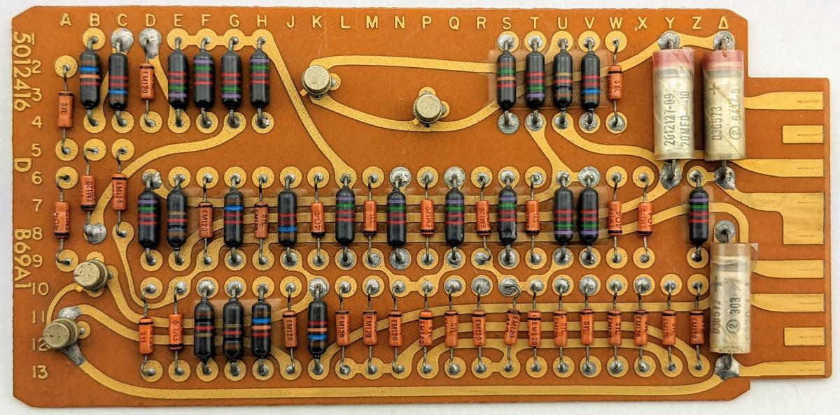
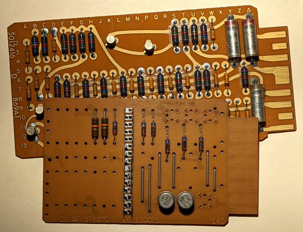
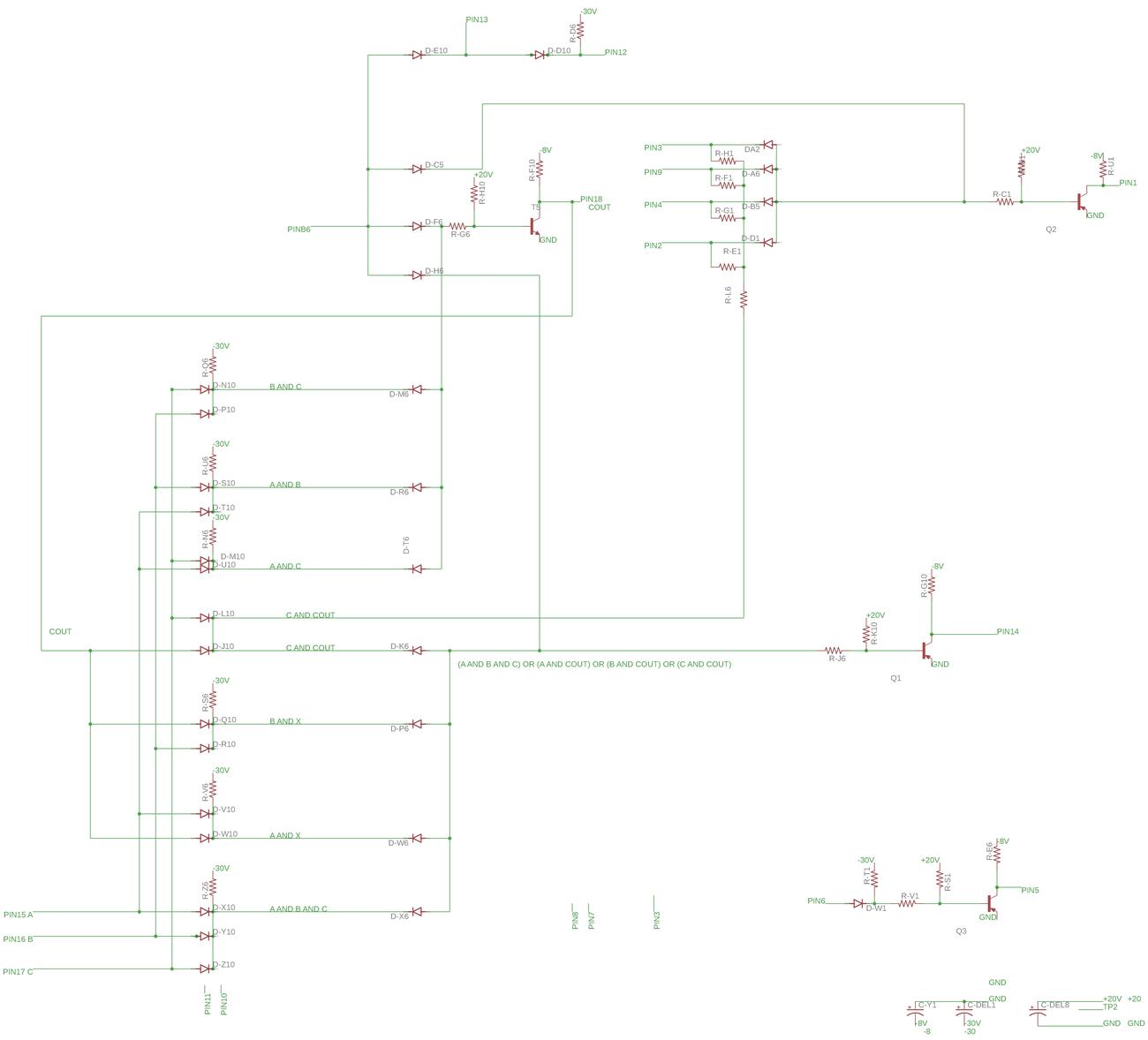
The IBM 1401 team at the Computer History Museum accumulates a lot of mystery components from donations and other sources. While going through a box, we came across the unusual circuit board below. At first, it looked like an IBM SMS (Standard Modular System) card, the building block of IBM's computers of the late 1950s and early 1960s.1 However, this board is larger, has double-sided wiring, the connector is different, and the labeling is different.2

The circuit board is about 15cm×7.3cm.

The circuit board is about 15cm×7.3cm.

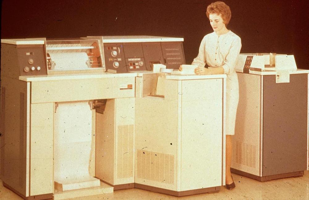
I asked around about the board and Robert Garner identified it as from the Univac 1004, a plugboard-controlled data processing system from 1963.4 The Univac 1004 was marketed as a "Card Processor" rather than a computer,3 designed for business applications that read punch cards and producing output, but still required calculation and logical decisions. Typical applications were payroll, inventory, billing, or accounting.

Photo of the Univac 1004. From bitsavers.

Photo of the Univac 1004. From bitsavers.

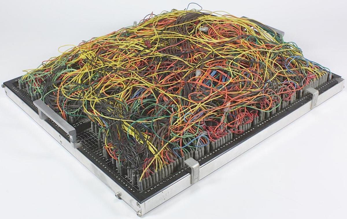
The most unusual feature of the Univac 1004 was that it was programmed by a plugboard (below) instead of a stored program. The system was programmed by plugging patch cords into a plugboard to indicate the desired action for each of the 31 program steps. While earlier electromechanical accounting machines used plugboards, they were pretty much obsolete by 1963, so I was a bit surprised to see plugboards still in use.

A plugboard for the Univac 1004. This board was used for payroll consolidation from 1965 to 1972. From Museums Victoria Collections, Copyright Museums Victoria / CC BY 4.0.

A plugboard for the Univac 1004. This board was used for payroll consolidation from 1965 to 1972. From Museums Victoria Collections, Copyright Museums Victoria / CC BY 4.0.

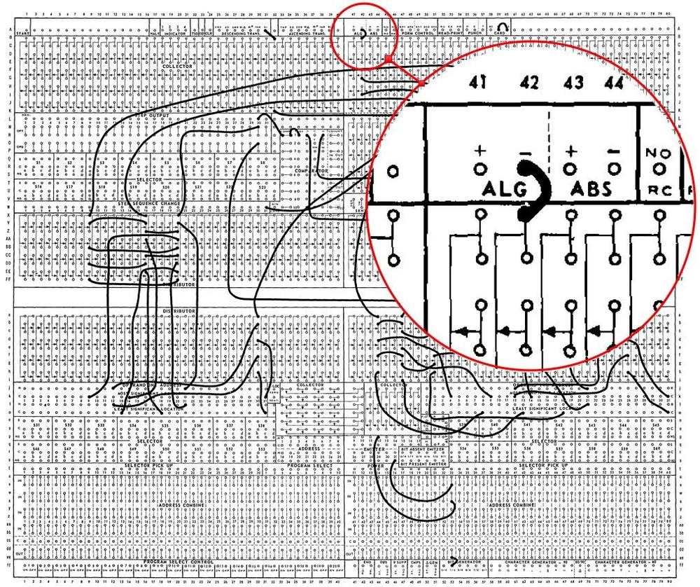
The computer's "program" consisted of 31 steps. The operations for each step were specified by plugging wires into the board. For instance, a data field could be moved from a punch card to memory, a value could be added or subtracted, or a line of output could be configured for the printer.5 The system even supported conditional branches. The diagram below shows the structure of the plugboard. The highlighted wire shows a subtraction operation, activated by the wire in the "algebraic minus" position.

Part of a program in the plugboard.  Click for a larger version. From the Reference Manual.

Part of a program in the plugboard. Click for a larger version. From the Reference Manual.

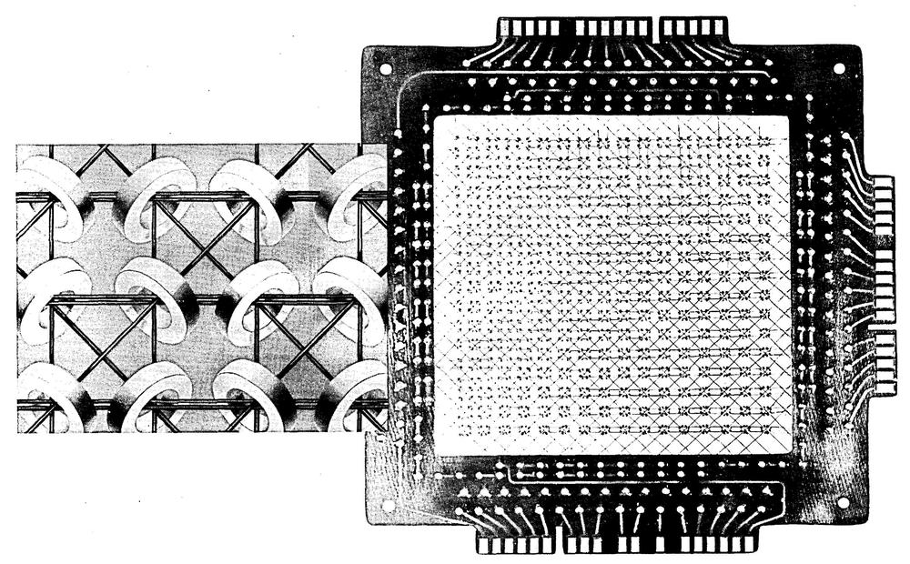
The computer had a small memory of 961 6-bit characters. Like most computers of the era, it used magnetic core memory, storing each bit by magnetizing a tiny ferrite ring. Note that since the computer was programmed through a wiring panel, none of the memory was used for program code.

A plane of magnetic core storage, from the Reference Manual.

A plane of magnetic core storage, from the Reference Manual.

While the Univac 1004 was primitive for its time compared to even a low-end business computer like the IBM 1401, it had a few advantages. First, it rented for $1900 a month, compared to $2500 a month for the IBM 1401 (about $18,000 vs $23,000 a month in current dollars). Second, the Univac computer was compact (by 1960s standards), weighing 2500 pounds. Finally, many customers found plugboard programming easier than programming with code, both because they were more familiar with it and because it is visual and direct.

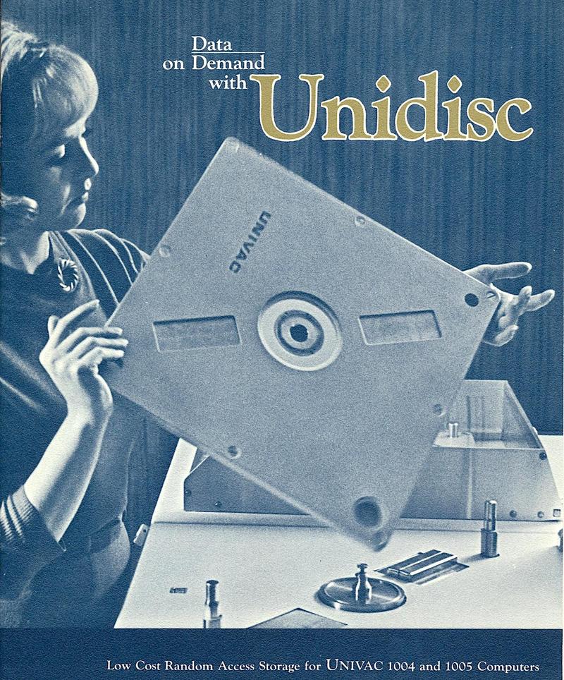
The Univac 1004 could be extended with peripherals such as tape drives, a card punch, or disk storage. The photo below shows the Unidisc cartridge, which held one million characters. Although it looks like an absurdly-large floppy disk, it was a removable hard disk.

The Unidisc cartridge is 15¾ inches square and ⅝-inch thick. (source).

The Unidisc cartridge is 15¾ inches square and ⅝-inch thick. (source).

Reverse-engineering the board

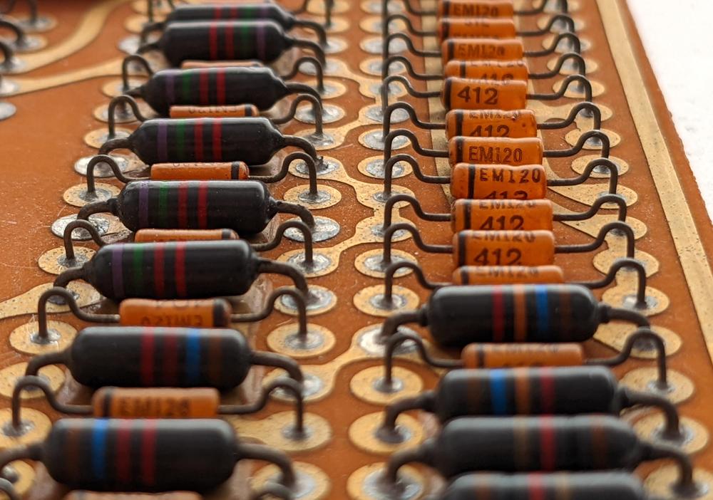
The function of the board wasn't immediately obvious and we had various theories of what it might do. To find out, I reverse-engineered the board by tracing out the circuitry.6 The board has 32 diodes, which seems like a lot, as well as resistors, transistors, and capacitors. The transistors are not silicon transistors, but germanium PNP transistors.

A closeup of the circuit board showing resistors and diodes.

A closeup of the circuit board showing resistors and diodes.

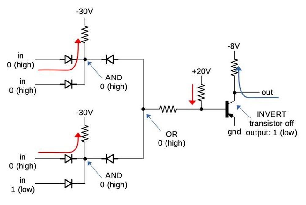
The board turned out to be a logic board implemented with AND-OR-INVERT logic.7 That is, various inputs are ANDed together, the AND results are then ORed together, and finally the result is inverted. The board is implemented with diode-transistor logic. One layer of diodes implements the AND gates and the second layer of diodes implements the OR gates. Finally, a transistor amplifies the result, inverting it in the process. Diode-transistor logic (DTL) performed better than earlier resistor-transistor logic (RTL), but was soon replaced by transistor-transistor logic.

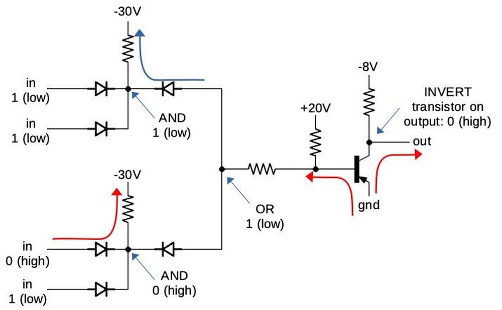
The diagram below explains how the AND-OR-INVERT logic was implemented. This circuit has four inputs: two AND gates that are then ORed together and inverted. (It's a bit confusing because the circuit uses active-low logic, so the voltage levels are all inverted.) If the AND gates all have a 0 (high) input, a diode in the first stage will conduct and pull the AND node high. This blocks the diodes in the second stage (which have the opposite orientation), so the OR node is also high. In the INVERT stage, the +20V resistor will pull the transistor's base high, which turns it off (since it is PNP). Finally, the -8V resistor will pull the output low (i.e. 1), providing the desired AND-OR-INVERT logic.

The AND-OR-INVERT logic producing a 1 output.

The AND-OR-INVERT logic producing a 1 output.

The diagram below shows that if the first AND gate's inputs are 1 (low), the first diodes are blocked, so the -30V resistor pulls the AND node low (1). Now the second-stage diode conducts, pulling the OR node low (1). This allows base current to flow through the PNP transistor, turning it on. This pulls the output high (0). (Note that ground is a high output compared to the low output of -8V.) The gates on the board have more inputs, but use the same principle.

The AND-OR-INVERT logic producing a 0 output.

The AND-OR-INVERT logic producing a 0 output.

After tracing out the board's logic, I recognized that it implemented a full adder.8 That is, it adds two input bits along with a carry-in, producing a sum bit and a carry-out. By connecting four full-adders in series, a 4-bit value can be added, allowing one decimal digit to be added. Thus, the computer probably has four one-bit adder boards similar to this, along with circuitry to convert the output from binary to binary-coded decimal.10

The board has a few additional circuits along with the full adder circuit. It includes an inverter circuit. The board also has 4 inputs that are ANDed, subject to the carry value. Finally, the board also has a disable input that blocks the outputs.9 Without knowing more about the circuitry, I can't determine the role of these circuits.

Conclusion

The mystery circuit board turned out to be from the Univac 1004. Although this computer was produced in the 1960s, its technology occupies an interesting location between the electro-mechanical accounting machines of the 1940s and the electronic business computers of the late 1950s. The Univac computer used transistors and core memory, but it kept the earlier plugboard programming of the accounting machines, rather than moving to stored-program computing (introduced in 1948). Even though the Univac 1004 was technologically backward for 1963, businesses flocked to it, making it the second-most popular computer at the time with 3400 installations.4

This shows that progress isn't as linear as you might expect; "obsolete" technologies can continue to thrive long after the introduction of "superior" alternatives such as stored-program computing. Instead, new systems can still be developed with supposedly-obsolete technologies, depending on the tradeoffs involved.

I announce my latest blog posts on Twitter, so follow me @kenshirriff. I also have an RSS feed.

Notes and references

  1. The Computer History Museum links to a similar board

  2. The photo below compares the Univac board to a smaller IBM SMS board.

    Comparison with an IBM SMS card.

    Comparison with an IBM SMS card.


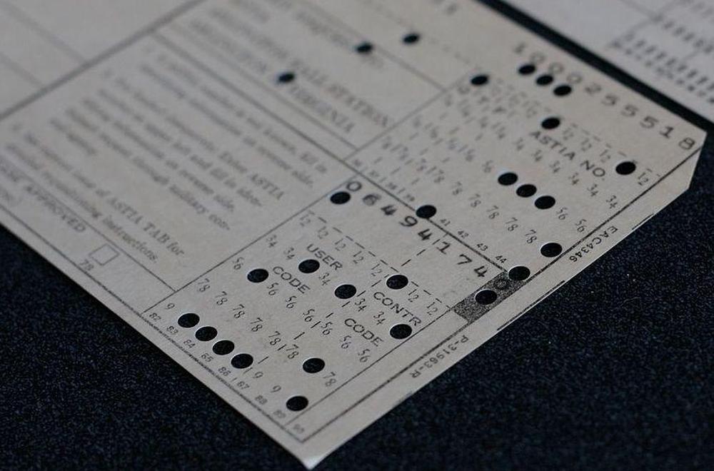
  3. The Univac 1004 computer came in two versions. The "80" read standard IBM 80-column punch cards. The "90" read Univac's 90-column cards (details), which held 90 characters per card instead of 80. The 90-column card was introduced in 1930 by Remington Rand. It had round holes instead of IBM's rectangular holes. The card stored two characters per column by using a denser, binary code. Despite the superior capacity of the 90-column card, IBM's 80-column cards dominated the market. (Even IBM couldn't displace the 80-column card, although they tried with the 96-column card that they introduced in 1969.)

    A 90-column punch card. From Marcin Wichary,  (CC BY 2.0).

    A 90-column punch card. From Marcin Wichary, (CC BY 2.0).


  4. Robert Garner discusses the Univac 1004 briefly in his article on Early Popular Computers. More information is in the 1964 BRL report as well as on Bitsavers. A related board from the Univac 1040/1050 is described here

  5. The plugboard supported conditionals and looping, so I think the system was Turing-complete, although you couldn't do a lot in 31 programming steps. You could implement multiplication or division with a short shift and add (or subtract) loop. 

  6. To reverse-engineer the board, I took photos of both sides, flipped the image of the back in GIMP so the two sides were aligned visually, arranged the components on a schematic in EAGLE, and connected the components to match the circuit board. Then I moved the components around until the layout made sense.

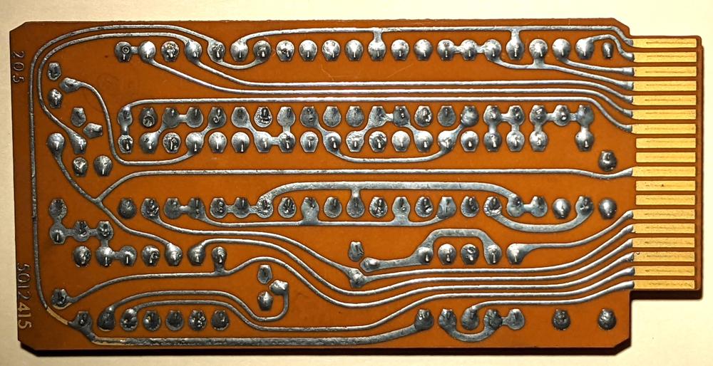
    The underside of the circuit board.

    The underside of the circuit board.

    The back of the circuit board is shown above. Note that the edge connectors are completely different on the two sides of the board.


  7. AND-OR-INVERT logic was also used in the IBM System/360 computers, although it was built from hybrid SLT modules instead of discrete components. 

  8. I suspected the board was an adder when I saw that it had three inputs and was combining them symmetrically. The full adder is implemented in AND-OR-INVERT logic as follows. If the two bits are A and B and the carry-in is CIN, then a carry-out (COUT) is generated if at least two input bits are set. This is computed by the AND-OR logic "(A and B) or (A and CIN) or (B and CIN)". The sum bit is set if there is a single 1 input or three 1 inputs. The sum bit was computed by "(A and not COUT) or (B and not COUT) or (CIN and not COUT) or (A and B and CIN)" As a result of the AND-OR-INVERT circuit, the output is inverted. The inverter circuit on the board was probably used to un-invert it. 

  9. The full reverse-engineered schematic is below.

    Reverse-engineered schematic of the board. Click for a larger version.

    Reverse-engineered schematic of the board. Click for a larger version.


  10. The computer uses excess-three encoding for digits, adding 3 to the value before converting to binary. For example, 6 is represented as binary 1001. The advantage of this encoding is that flipping the bits yields the 9's-complement decimal value, simplifying subtraction. For example, flipping the bits of 6 yields binary 0110, which is 3 in excess-3 notation. Excess-3 representation also handles carries correctly; if you add two numbers that sum to 10, the excess-3 values will sum to 16, causing a binary carry. To convert the sum to excess-3, The value 3 must be added (if a carry) or subtracted (if no carry).

    To see how addition works with excess-3, 2 + 4 in excess-3 is binary 0101 + 0111 = 1100. Subtracting 3 yields 1001, which is 6 in excess-3. But 2 + 9 is binary 0101 + 1100 = 10001, generating a carry out of the 4 bit value. Adding 3 yields 0100, which is 1 in excess-3. Considering the carry-out, this is the desired result of 11. 

Simulating the IBM 360/50 mainframe from its microcode

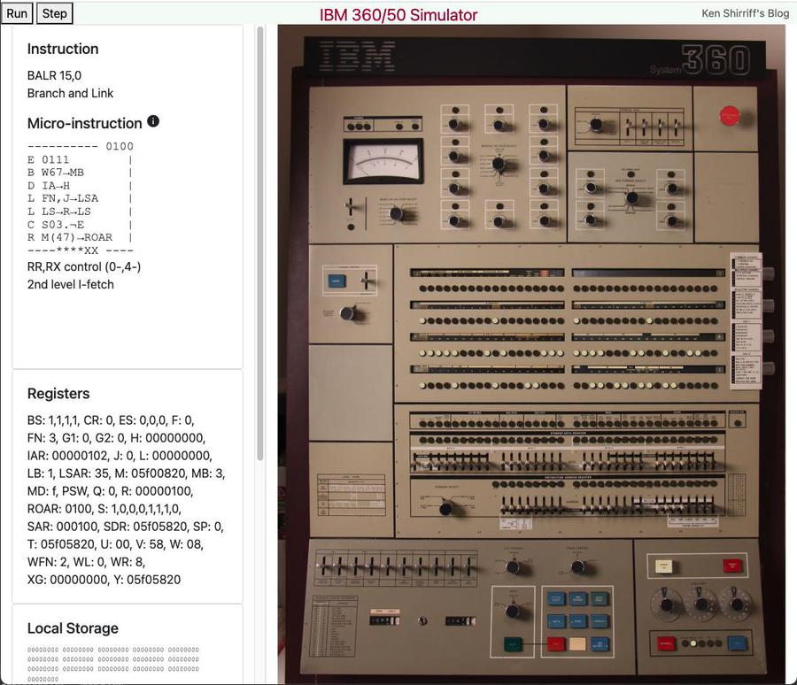
The IBM System/360 was a groundbreaking family of mainframe computers announced on April 7, 1964. System/360 was an extremely risky "bet-the-company" project for IBM, costing over $5 billion, but the System/360 ended up as a huge success, setting the direction of the computer industry for decades. The S/360 architecture was so successful that it is still supported by IBM's latest mainframes, almost 60 years later. I'm developing a microcode-level simulator1 for the IBM System/360 Model 50 (link to the simulator); this blog post provides background to understand the Model 50 and the simulator.

Screenshot of the simulator running in a browser.

Screenshot of the simulator running in a browser.

The radical decision behind System/360 was to use a single architecture for the entire product line of computers.3 The name symbolized “360 degrees to cover the entire circle of possible uses.” Using a common architecture seems obvious now (e.g. x86), but prior to the System/360, IBM (like other computer manufacturers) produced multiple computers with entirely incompatible architectures.

Internally, the different System/360 models had completely different implementations to support a wide range of cost and performance levels: the fastest model was over 1000 times as powerful as the slowest. Low-end models used simple hardware and an 8-bit datapath while advanced models used wide datapaths, fast semiconductor registers, out-of-order instruction execution, and caches.2 Despite these internal differences, the models all looked the same to the programmer.

Architecture of System/3604

You might expect a computer architecture from the 1960s to be simple, but System/360 is remarkably complex, partly because it merged six computer families into one architecture. It is a 32-bit architecture that supports many datatypes. As well as 32-bit integers and half words, it supports decimal arithmetic on numbers up to 31 digits long. Floating-point arithmetic supports short (32 bit), long (64 bit), or extended (128 bit) values. The processor also supports character strings up to 256 bytes long.

The System/360 instruction set has about 100 different instructions and several addressing modes. Some of these instructions are straightforward arithmetic, logic, or control operations. Other instructions are more complex, such as the "character move" that copies up to 256 characters in memory, or the floating-point instructions.

One of the most complex instructions is "edit", which formats a sequence of decimal digits for printing, for example inserting commas, a minus sign, or decimal point; removing leading zeroes, or filling leading spaces with characters. The number 1234567 could be "edited" into the string "$***12,345.67" for printing on a check. Keep in mind that this is a single instruction, not a library function like printf.

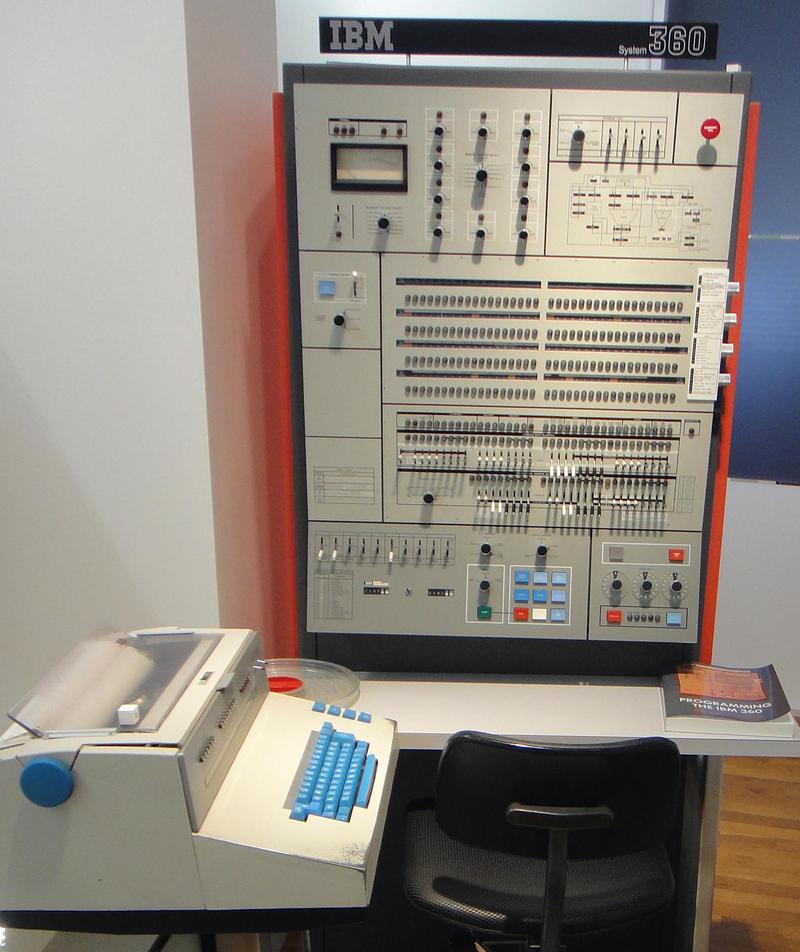
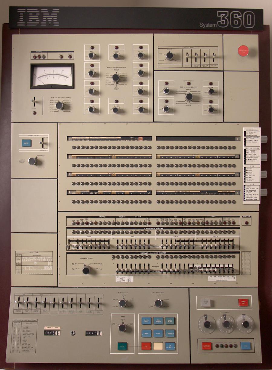
IBM System/360 Model 50 control panel. The dataflow diagram in the upper right illustrates the system's internal design. Photo by Sandstein, CC BY-SA 3.0.

IBM System/360 Model 50 control panel. The dataflow diagram in the upper right illustrates the system's internal design. Photo by Sandstein, CC BY-SA 3.0.

The System/360 architecture also included I/O, defining IBM's "channel" architecture. A channel is a programmable I/O subsystem with its own instruction set. On larger systems, the channel was an independent unit connected to the computer. But smaller systems such as the Model 50 used the same microcode engine to run CPU programs and channel programs.

The point is that System/360 has a large and complex instruction set. A single instruction could result in hundreds of memory accesses and processing steps. The dense instruction set helped programmers to cram programs into the extremely limited core memory of the 1960s. However, the complex instruction set was a problem for the computer designer, who had to implement the complex circuitry to carry out these instructions. The solution was microcode.

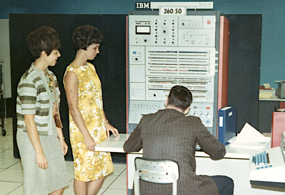
The System/360 Model 50 in a datacenter. The console and processor are at the left. An IBM 1442 card reader/punch is behind the IBM 1052 printer-keyboard that the operator is using. At the back, another operator is loading a tape onto an IBM 2401 tape drive. Photo from IBM.

The System/360 Model 50 in a datacenter. The console and processor are at the left. An IBM 1442 card reader/punch is behind the IBM 1052 printer-keyboard that the operator is using. At the back, another operator is loading a tape onto an IBM 2401 tape drive. Photo from IBM.

Microcode

One of the hardest parts of computer design is creating the control logic that tells each part of the processor how to carry out each instruction. In 1951, Maurice Wilkes came up with the idea of microcode: instead of building the control circuitry from complex logic gates, the control logic could be replaced with code (i. e. microcode) stored in a special memory called a control store. To execute an instruction, the computer internally executes several simpler microinstructions, specified by the microcode. Microcode turns the processor's control logic into a programming task instead of a logic design task.5

Microcode played a key role in the success of the System/360, helping IBM produce a line of computers with the same instruction set architecture but widely different implementations. It also allowed a processor to support different instruction sets; System/360 machines could be backward compatible with customers' older machines6 so customers could keep their existing software. For these reasons, the System/360 computers used microcode unless there was a compelling reason not to.7

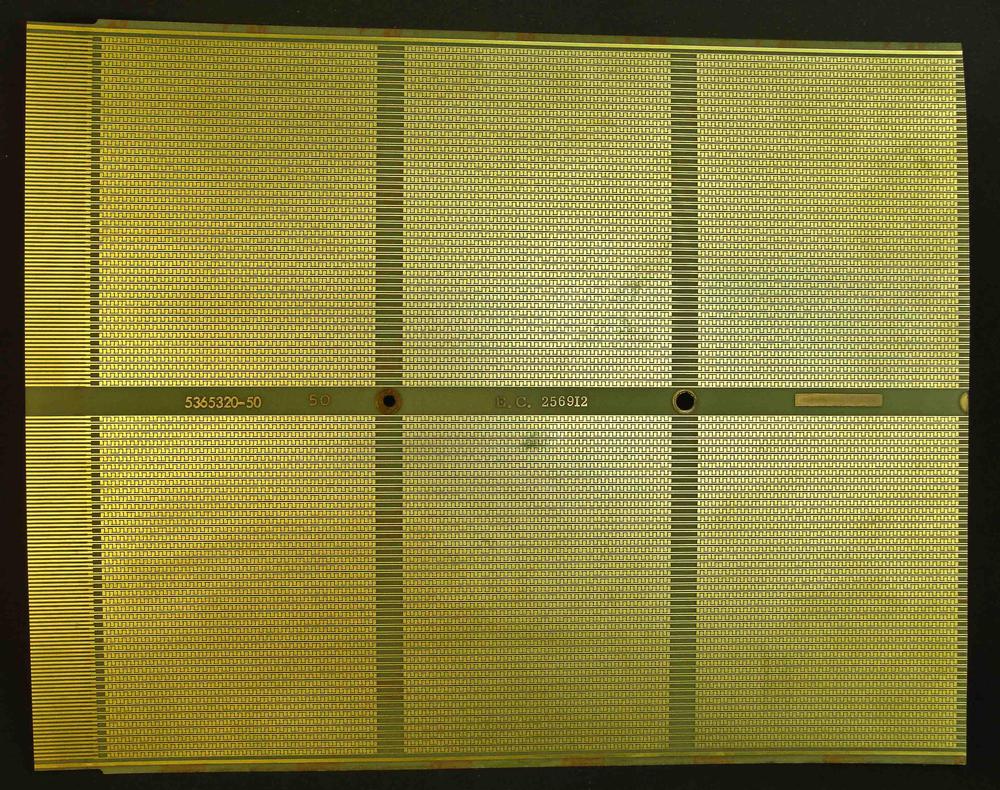
Another advantage of microcode is that it provides an easy way to fix design flaws and bugs in the field. Instead of modifying the hardware, a service engineer could replace the microcode with a new version. The photo below shows a copper sheet with microcode etched into it for the Model 50.

A replaceable BCROS sheet, holding 17,600 bits. Photo courtesy of Glenn's Computer Museum.

A replaceable BCROS sheet, holding 17,600 bits. Photo courtesy of Glenn's Computer Museum.

Microcode can be implemented in a variety of ways. Many computers use "vertical microcode", where a microcode instruction is similar to a machine instruction, just less complicated. The System/360 designs, on the other hand, used "horizontal microcode", with complex, wide instructions of up to 100 bits, depending on the model. These microinstructions were more like a collection of fields, each controlling low-level signals. This improved performance since multiple parts of the processor could be controlled in parallel.

Hardware of the Model 508

The Model 50 was roughly in the middle of the System/360 lineup, providing a powerful mainframe that could be used by a medium-sized business or university department. The Model 50 typically rented for about $18,000 - $32,000 per month (equivalent to $120,000-$200,000 a month in current dollars).

IBM S/360 Model 50. The console was attached to the main frame, about 5 feet deep. The storage frame and power frame are the black cabinets at the back. Photo from Pinterest.

IBM S/360 Model 50. The console was attached to the main frame, about 5 feet deep. The storage frame and power frame are the black cabinets at the back. Photo from Pinterest.

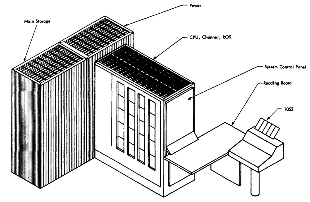
The Model 50 occupied three large cabinets, each 5 feet long, about 2 feet wide, 6 feet tall, and weighing nearly a ton each.9 The main frame, behind the console, contained the CPU, I/O channel circuitry, and the microcode storage. Behind this, the power cabinet contained the computer's power supplies. To the left, the cabinet at the back contained the main storage: one or two core memory modules, each with 128 kilobytes of memory. (I wrote in detail about the Model 50's core memory earlier.) The computer's cables ran under a raised floor to the I/O devices, which typically included tape drives, a card reader, printers, disk drives, I/O controllers, and so forth.

This diagram shows the three frames that made up the basic S/360 Model 50. Source: Model 50 Maintenance Manual page 138.

This diagram shows the three frames that made up the basic S/360 Model 50. Source: Model 50 Maintenance Manual page 138.

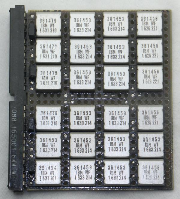
The System/360 processors weren't implemented with integrated circuits, but with SLT (Solid Logic Technology) modules, hybrid modules that contain a few transistors, diodes, and resistors. A typical module implemented a logic gate, so it takes many circuit boards full of modules to construct the processor.

A logic board using SLT modules. Each square metal can is a module.

A logic board using SLT modules. Each square metal can is a module.

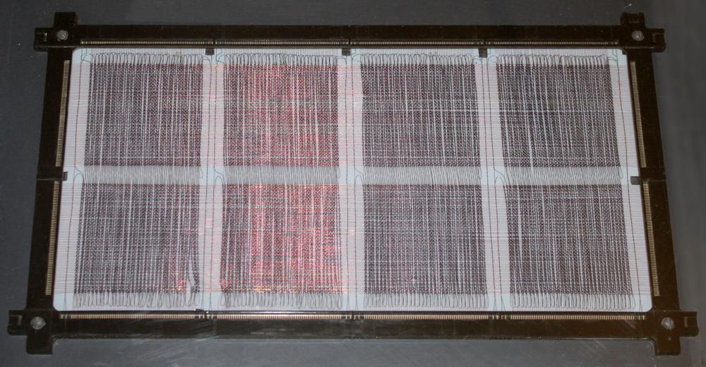
Like most computers of the 1960s, the Model 50 used magnetic core memory, with a tiny ferrite ring to store each bit. The photo below shows a core plane that stores 32768 bits (along with 512 bits for I/O). A stack of 18 planes formed a 64-kilobyte memory module, with two parity bits.10

A Model 50 core plane is arranged as a grid of cores. The Y lines run horizontally. X and sense/inhibit lines run vertically. The sense/inhibit lines form loops at the top and bottom. Each of the four vertical pairs of blocks has separate sense/inhibit lines. Each core plane was about 10¾ × 6¾ × ⅛ inches.

A Model 50 core plane is arranged as a grid of cores. The Y lines run horizontally. X and sense/inhibit lines run vertically. The sense/inhibit lines form loops at the top and bottom. Each of the four vertical pairs of blocks has separate sense/inhibit lines. Each core plane was about 10¾ × 6¾ × ⅛ inches.

The Model 50's internal architecture

To the programmer, all processors within System/360 look the same; internal circuitry, however, may be entirely different.

It's important to keep in mind that the internal architecture of the Model 50 is very different from the architecture that the programmer sees.11 In particular, the processor's internal registers are invisible to the programmer. The programmer instead sees 16 general-purpose registers and 4 floating-point registers, but to the processor these are part of the 64-word local store, a small high-speed core memory.

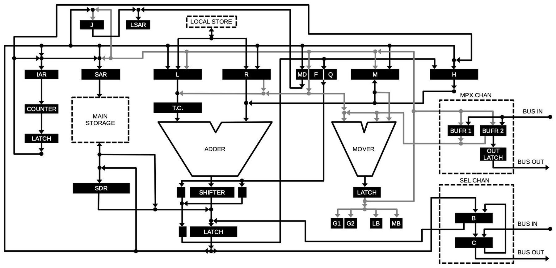
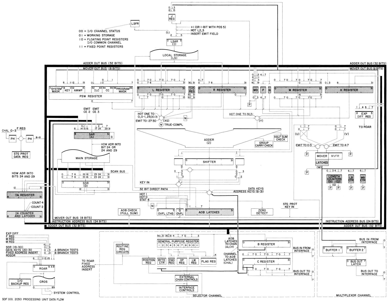
The diagram below shows the complex data flow through the computer.12 The black boxes are internal registers; the processor has a surprisingly large number of registers, used for a variety of purposes. The internal components are connected by buses. Most of the internal communication is over the 32-bit buses, shown in black. The 8-bit "mover" bus is shown in gray.

This diagram shows the data flow through the IBM 360/50 and appears in the upper-right corner of the console. I drew this version since I couldn't find a clear photo of it.

This diagram shows the data flow through the IBM 360/50 and appears in the upper-right corner of the console. I drew this version since I couldn't find a clear photo of it.

The heart of the computer is the 32-bit adder, which performs addition. For subtraction, the argument is complemented by the True/Complement circuit (TC). The adder has an associated shifter to perform bit-shifts; this is especially important for multiplication, division, and floating-point calculations. Operating in parallel with the adder is the "mover", which operates on bytes. It can extract a byte from a 32-bit word, as well as manipulating 4-bit pieces of the byte. The mover also performs Boolean operations (AND, OR, XOR). (Unlike most processors, the Model 50 separates arithmetic and logical operations, instead of having an ALU perform both.)

The computer's main core-memory storage is on the left. To access memory, an address is put in the Storage Address Register (SAR). Data is then read or written through the Storage Data Register (SDR). To the left of main storage, is the Instruction Address Register (the Program Counter or PC in modern terms). At the top is the Local Store, 64 words of high-speed core memory that holds the programmer's registers as well as some internal storage. The local store is accessed through the Local Store Address Register (LSAR).

At the right are the I/O channels: the low-speed Multiplexor Channel and the high-speed Selector Channel. You can think of these as DMA (direct memory access) paths for I/O. The multiplexor channel communicates over an 8-bit bus through the mover, while the selector channel communicates over a 32-bit bus. Although the channels are conceptually separate from the processor, the channels use the same buses, circuitry, and microcode engine as the processor. This limits I/O performance compared to more advanced System/360 models that have independent circuitry for the channels.

An example of the microcode

As you can see, the processor has many registers and functional units. The microcode needs to control these components to carry out program instructions. The microcode architecture is very complex and takes over 100 pages to explain thoroughly,15 so I'm only able to scratch the surface here. Each microinstruction is 90 bits long and performs multiple tasks. In the documentation, IBM used an 11-line block to represent each microinstruction, showing all the activities that are taking place in parallel.

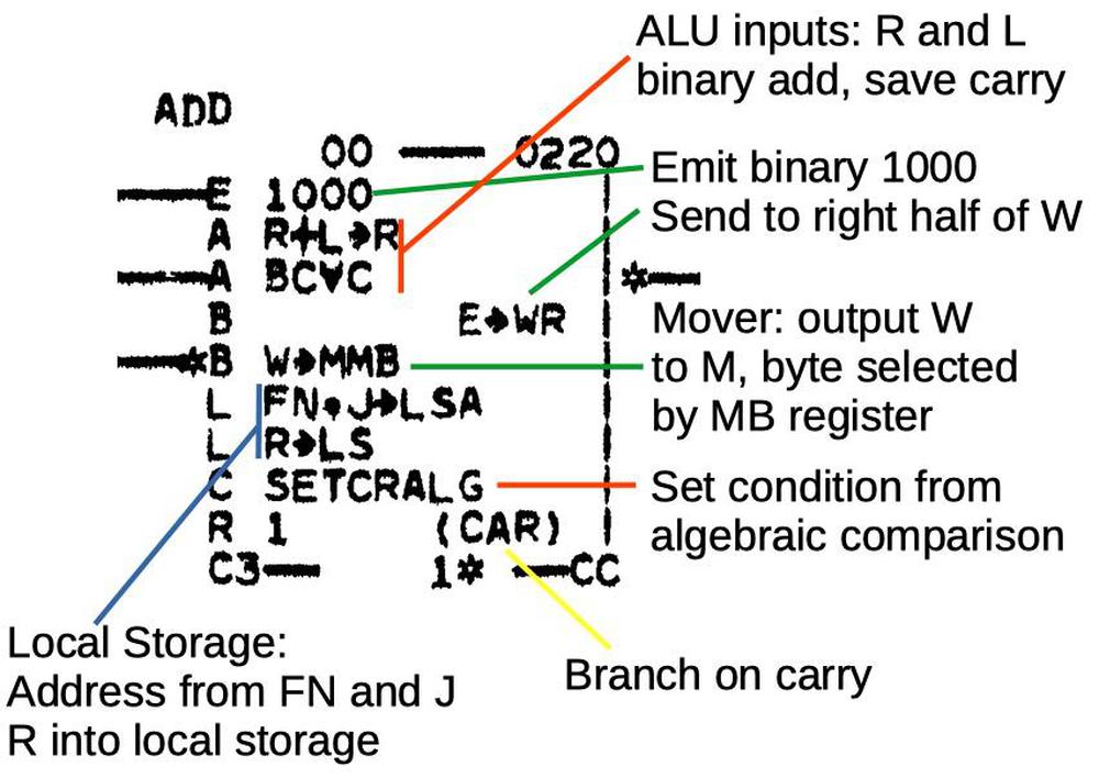
A sample microinstruction is shown below, part of the microcode that implements an add instruction. At this point, earlier microinstructions have fetched and decoded the instruction and put the arguments into the R and L registers. This microinstruction performs the actual 32-bit addition, but there's a lot more happening than just the addition.

One microinstruction, part of the integer addition code. This microinstruction is at micro-address 0220.

One microinstruction, part of the integer addition code. This microinstruction is at micro-address 0220.

Starting with the line "R+L→R" (red), this indicates that the ALU is taking inputs from registers R and L, and the result is going into the R register. In other words, the two arguments are added. The result R is stored into the desired programmer-visible register in local storage (blue). The processor registers FN and J select the address in local storage. Meanwhile, the SETCRALG line sets the Condition code register based on the sign (i.e. "algebraic" value) of the result, indicating if the result is positive, negative, or zero.

The line "BC⩝C" indicates that signed overflow is detected and used as the carry flag14 while CAR (yellow) indicates the microcode branches on this carry (overflow) value. Thus, the microcode will take one path if the addition was valid and a second error path if overflow occurred. A microinstruction can "emit" an arbitrary 4-bit value (green) which can be used in a variety of ways. In this case, the binary value 1000 is emitted, fed into the W register, and then the M register, for use by the next microinstruction. As you can see, the CPU performs many activities in parallel for one microinstruction, which increases the computer's performance.

All the activities of a microinstruction are encoded into a 90-bit word consisting of 28 fields.13 The microinstruction discussed above (micro-address 0220) is highlighted in the documentation below. A single microinstruction is very complex, which is why it takes an 11-line block of text to represent it.

Part of the microcode listing. The previously-discussed microinstruction is highlighted. Note that the micro-address 0220 matches the address in the upper-left corner of the microinstruction diagram.

Part of the microcode listing. The previously-discussed microinstruction is highlighted. Note that the micro-address 0220 matches the address in the upper-left corner of the microinstruction diagram.

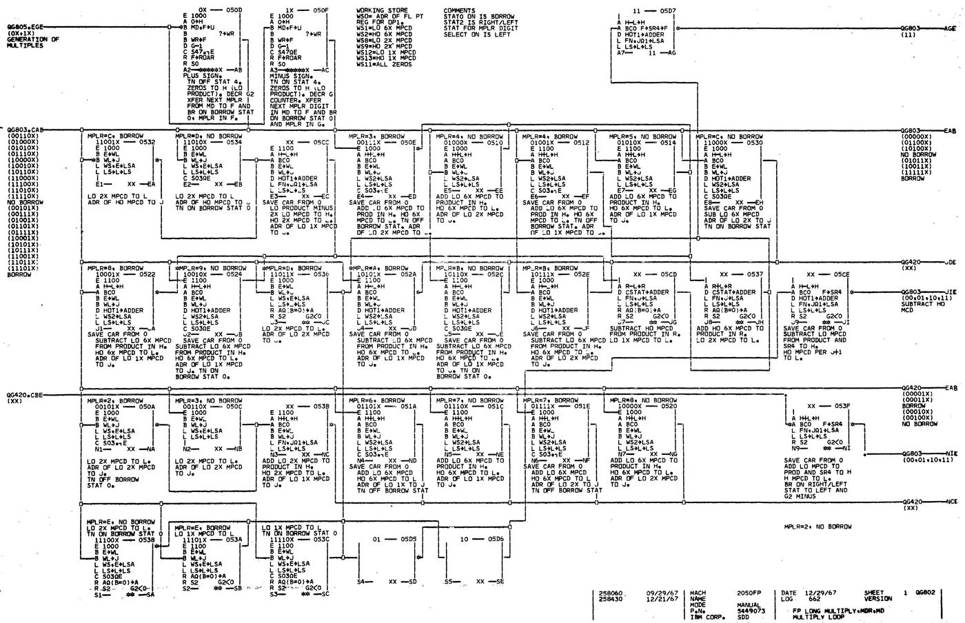
The processor documentation contains hundreds of pages of microcode;16 one page of the floating-point multiply code is below. Each box is one microinstruction, and the lines between them indicate the complex control paths. I'm not going to explain this microcode,17 but I wanted to show its complexity.

Part of the floating-point multiply microcode. (Click for a larger view.) From ALD vol 18.

Part of the floating-point multiply microcode. (Click for a larger view.) From ALD vol 18.

The console

The discussion above has shown the complex internal architecture of the Model 50. The numerous lights and controls on the console19 provide a view into this internal state. There were three main uses for the console. The first use was basic "operator control" tasks such as turning the system on, booting it, or powering it off, using the controls in the lower section of the console. These controls were consistent across the S/360 line and were usually the only controls the operator needed. The three hexadecimal dials in the lower right selected the I/O unit that held the boot software. Once the system had booted, the operator generally typed commands into the system rather than using the console.

Control panel of the IBM System/360 Model 50. This panel has marginal check controls for auxiliary storage in the upper right, replacing the dataflow diagram.

Control panel of the IBM System/360 Model 50. This panel has marginal check controls for auxiliary storage in the upper right, replacing the dataflow diagram.

The second console function was "operator intervention": program debugging tasks such as examining and modifying memory or registers and setting breakpoints. The lights and toggle switches in the lower half of the console were used for operator intervention. The operator could enter a 24-bit address using the row of 24 toggle switches, and enter a 32-bit data value using the row of 32 toggle switches above. The lights allowed the contents of memory to be examined. With other switches, the operator could set a breakpoint, single-step through a program, and perform other debugging operations.

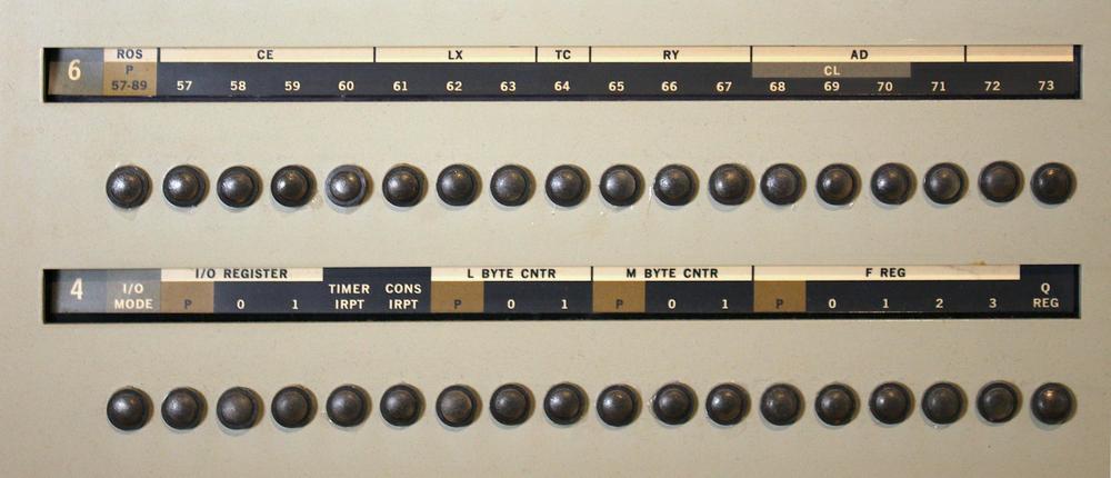
The third console function was system maintenance and repair performed by an IBM customer engineer. The customer engineering displays took up the top half of the console and provided detailed access to the computer's complex internal state. To save space, the Model 50 had four roller knobs on the right side, with 8 positions for each knob. Each knob position selected a different function for the row of 36 lights (32 bits plus parity). The legends above the lights rotate with the knobs, showing the meaning of each light. For example, one position would display the L register, while another position would display the current microinstruction. In the photo below, the upper roller and lights are displaying part of the microcode currently being executed (ROS = Read Only Store). The roller below shows some of the internal registers and counters.

Closeup of two rollers and the associated lights.

Closeup of two rollers and the associated lights.

Finally, the voltmeter and voltage control knobs in the upper left of the console were used by an IBM customer engineer for "marginal checking". By raising and lowering the voltage levels, borderline components could be detected and replaced before they caused problems.

The simulator

The simulator is at righto.com/360 and the code is on Github. I implemented the simulator in JavaScript so it can run in a browser. It runs a sample program by executing the Model 50's microcode, simulating each microinstruction and the hardware. Each microinstruction is displayed graphically, along with the current instruction, the registers, the local storage, and core memory. It displays the console lights accurately based on the internal state, on a zoomable virtual console. Each row of lights can display 8 different elements, which you can change by clicking on a roller. You can step also through the microcode, one microinstruction at a time.

This simulator is still under development so don't expect it to work perfectly. I also haven't implemented the toggle switches, so you can't enter a program from the console yet. I also need to implement the I/O system, which has its own registers and a different microcode format.

To build the simulator, I extracted the binary microcode from the listings using a custom OCR tool. I implemented the hundreds of micro-operations, which were tricky to get correct. While most micro-operations are simple operations such as moving a register to the bus, some microinstructions are much more complex, especially for floating-point operations.20 Another complication is that a microinstruction performs many tasks in parallel and it was hard to determine the exact order in which to perform them.

My eventual goal with the simulator is to move it into the physical world. Specifically, I plan to drive the lights on CuriousMarc's Model 50 control panel to make the panel operate accurately. We also plan to hook up his IBM tape drives and card reader so we can have all the pieces of a Model 50 mainframe working together, except for the processor itself. I plan to port the simulator to C so I can run it in a microcontroller to drive the physical console. An FPGA implementation is another possibility; this would provide the maximum speed, but would be harder to implement.

I announce my latest blog posts on Twitter, so follow me @kenshirriff for updates and future articles. I also have an RSS feed. Thanks to Richard Cornwell for discussion and data.

Notes and references

  1. My simulator is not particularly useful unless you really care about the microcode in the Model 50. If you want to run software on a simulated System/360, you probably want to use the Hercules system

  2. I'll briefly summarize some of the different implementations used in System/360 computers.

    The low-end Model 30 uses an 8-bit bus and ALU, so 32-bit operations take four steps. It uses 60-bit microcode.

    The Model 40 also has an 8-bit bus and ALU, but it has 16-bit registers and a 16-bit bus to memory, improving the performance. It has 60-bit microcode.

    The Model 50 (discussed in this blog post) has 32-bit registers, memory bus, and adder. It also has the 8-bit mover that can operate in parallel with the adder.

    The Model 65 has a 64-bit bus, and multiple adders (60 and 8-bit) that allow a floating-point fraction and exponent to be processed in parallel. It also has an 8-byte instruction buffer and external channels. It uses 100-bit microcode.

    The Model 75 has a 64-bit main adder, 8-bit exponent adder, 8-bit decimal adder, and a 24-bit addressing adder. It overlaps instruction fetching and execution, with 16 bytes of instruction prefetching and 8 bytes of data prefetching.

    The high-end Model 91 has an advanced superscalar architecture with out-of-order execution, instruction pipelining, and multiple arithmetic execution units. Higher models support memory interleaving for faster access: 2-way on the Model 65 up to 16-way on the Model 195.

    The models 44, 75, 91 and above used hardwired control instead of microcode to squeeze out more performance.

    As you can see, the System/360 line has a wide variety of implementations. At the low end, the hardware is kept to a minimum to reduce costs, while at the high end, more hardware boosts performance, with wider datapaths and multiple functional units providing parallelism. 

  3. The System/360 line didn't completely meet the goal of a compatible architecture. IBM split out the business and scientific markets on the low-end machines by marketing subsets of the instruction set. The basic instructions were provided in the "standard" instruction set. On top of this, decimal instructions (for business) were in the "commercial" instruction set and floating-point was in the "scientific" instruction set. The "universal" instruction set provided all these instructions plus storage protection (i.e. memory protection between programs). Additionally, cost-cutting on the low-end Model 20 made it incompatible with the S/360 architecture, and the Model 44 was somewhat incompatible to improve performance on scientific applications. 

  4. IBM defined the System/360 architecture in great detail in a document called the IBM System/360 Principles of Operation. It describes not only the instruction set, but also the datatypes, input/output model, the interrupt model, and even the basic structure of the system control panel. To learn more about System/360, see A Programmer's Introduction to the IBM System/360 Architecture, Instructions, and Assembler Language. A bunch of assembly examples are at rosettacode

  5. The primary benefit of microcode for IBM was economic. As described in Microprogram Control for System/360, the cost of a non-microcoded processor is roughly linear in the size of the instruction set. However, a microcoded system has a roughly fixed cost, with a small overhead for additional instructions. Thus, as instruction sets get more complex (as in System/360), there is a crossover point where microcode is more efficient. This is especially the case for smaller systems where the base cost is lower. The lower marginal cost also makes emulating other systems more feasible. The IBM System/360 was one of the first commercial computers to make extensive use of microcode. 

  6. Various System/360 machines supported compatibility features with earlier IBM computers including the 1401, 1440, 1620, 7070, 7074, 7080, 709, 7090, 7094. Generally, a smaller System/360 machine could replace a smaller IBM computer such as the 1401, while a larger mainframe such as the 7090 needed to be replaced by a larger System/360 computer such as the Model 65.  

  7. A few System/360 models did not use microcode. The Model 44 was designed as a high-performance computer for scientific applications, so it used hardwired control. The Model 85 was partially microcoded, while the Models 75 and 91 were completely hardwired. 

  8. The book IBM's 360 and Early 370 Systems describes the history of the S/360 in great detail. IBM lists data on each model, including dates, data flow width, cycle time, storage, and microcode size. Another list with model details is here. The article System/360 and Beyond has lots of info. A list of 360 models and brief descriptions is here. For information on the Model 50 specifically, see the Functional Characteristics manual, Field Engineering manuals, Wikipedia, photos here and here, CuriousMarc video

  9. For detailed dimensions of the System/360 components, see the Physical Planning Manual For more memory, another 1500-pound frame could be added to the Model 50, boosting it from 256 kilobytes of memory to 512 kilobytes. Up to four Large Capacity Storage units (IBM 2361) could be added, each providing two more megabytes. 

  10. I wrote in detail about the Model 50's core memory system here

  11. The quote is from System/360 Model 40 comprehensive introduction

  12. The Model 50 Field Engineering Diagram Manual contains the detailed data flow diagram below. This diagram corresponds to the diagram discussed earlier, but provides much more detail. In particular, it shows the exact bit widths of the various data paths and registers.

    The detailed data flow diagram. Click for a larger version.

    The detailed data flow diagram. Click for a larger version.


  13. The table below shows how a microinstruction is encoded into a 90-bit word.

    BitsNameMeaning
    0PParity
    1-3LUMover input left side
    4-5MVMover input right side
    6-11ZPROAR address (Read Only storage Address Register)
    12-15ZFROAR branch control
    16-18ZNAddress control field
    19-23TRAdder control
    24Unused
    25-27WSLocal store address control
    28-30SFLocal store functions
    31PParity
    32-34IVInvalid digit test
    35-39ALAdder latch gating
    40-43WMMover destination
    44-45UPByte counter function
    46MDMD counter control
    47LBL byte counter control
    48MBM byte counter control
    49-51DGLength counter
    52-53ULMover function left digit
    54-55URMover function right digit
    56PParity
    57-60CEEmit field
    61-63LXLeft adder input
    64TCTrue or complement control
    65-67RYRight adder input
    68-71ADAdder function control
    72-77ABA branch control
    78-82BBB branch control
    83Unused
    84-89SSStat setting control

    For channel instructions, the microcode format is slightly different since some of the fields need to control the channel circuitry. However, most of the fields are the same as for the CPU. The table below shows the microcode format for the channel; the highlighted entries are different from the CPU microcode.

    BitsNameMeaning
    0PParity
    1-3LUMover input left side
    4-5MVMover input right side
    6-11ZPROAR address
    12-15ZFROAR branch control
    16-18ZNAddress control field
    19-23TRAdder control
    24Unused
    25CSLocal storage address selector
    26-27SALocal storage address
    28-30SFLocal storage function
    31PParity
    32-34CTTiming signals to channel
    35-39ALAdder latch gating
    40-42WLMover destination
    43-46HCMultiplexor channel stat setting
    47-48CGControl signals to channel
    49-51MGMultiplexor channel gate control
    52-53ULMover function left digit
    54-55URMover function right digit
    56PParity
    57-60CEEmit field
    61-63LXLeft adder input
    64TCTrue or complement control
    65-67RYRight adder input
    68-70CLSelector channel adder latch tests
    71Unused
    72-77ABA branch control
    78-82BBB branch control
    83Unused
    84-89SSStat setting control
     

  14. When adding twos-complement signed numbers, an overflow occurs if the carry out of the most significant bit is different from the carry out of the second-most-significant bit. (I explain this in detail here.) IBM numbers the bits in a word "backward" with bit 0 the most significant. Thus, an overflow occurs if the carry from bit 0 XOR'd with the carry from bit 1 is nonzero. IBM uses ⩝ to indicate an exclusive or. Thus, CARRY(0) ⩝ CARRY(1) indicates an overflow, represented as BC⩝C in the microcode. 

  15. For a description of how the Model 50 microcode works, see the book "Microprogramming: Principles and Practices", S. Husson (1970), pages 295 to 411. Bitsavers has a lot of Model 50 documents, but not everything. If you have additional documentation, such as the IBM Automated Logic Diagrams, please let me know. 

  16. The Model 50's microcode listing is available in three volumes on bitsavers. The binary microcode listings are difficult to read with OCR because pages were printed on different printers; some use serif fonts and others use sans-serif fonts. I made my own OCR program designed to process binary, which was able to read the listings for the most part. The presence of parity in the microcode helped catch errors. 

  17. Ok, I'll give a brief explanation of that page of microcode, which is part of the implementation of floating-point multiplication. The implementation is designed with tradeoffs between speed, code length, and temporary memory usage. The idea is to multiply the multiplicand by the multiplier, kind of like long multiplication on paper, where you multiply a digit at a time and add the partial sums. This code processes a hex digit of the multiplier at a time, with a separate case for each digit. The multiplicand is multiplied by the digit and this is added to the running total, shifting as appropriate. To make this fast, multiples of the multiplicand are pre-computed. However, pre-computing 16 multiples (one for each hex digit value) would take too much temporary (local) storage. So the only pre-computed multiples are 1, 2, and 6, and these are combined for other digits. To multiply by the digit 7, for instance, the multiples for 1 and 6 are added. To multiply by the digit 4, the multiple for 6 is added and the multiple for 2 is subtracted.

    But what about multiplying by 9 through 15? The trick is to "borrow" 16 from the next-higher digit. For instance, to multiply by the digit 11, you borrow 16, subtract the multiple for 6, and add the multiple for 1. Then the value one less is used for the next digit to account for the borrow. Thus, all 16 possibilities can be handled by adding or subtracting at most two of the pre-computed values. With borrowing, the code needs to handle 32 cases; the included page implements 22 of these cases. This implementation makes multiplication rapid, but the microcode is complex with many paths. (There is also a bunch more code to handle the floating-point exponent, normalizing values, overflow, underflow, and so forth.) 

  18. Different System/360 models used a variety of methods to store microcode.18 An important feature of IBM's microcode storage was that the microcode could be replaced in the field. The low-end Model 25 held microcode in a 16-kilobyte section of core memory called Control Storage. The Model 30 used CCROS (Card Capacitor Read-only Store), storing the microcode on special metalized punch cards that were read capacitively. Transformer Read-Only Storage (TROS, below) was used by the System/360 Model 20 and Model 40. I wrote an article about microcode storage if you want more information.

    A TROS module from an IBM System/360 Model 20.

    A TROS module from an IBM System/360 Model 20.

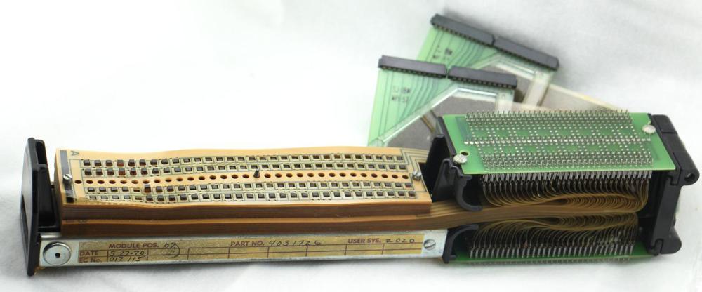
    The Model 50 (as well as 65 and 67) stored microcode in BCROS (Balanced Capacitor Read-Only Storage), using copper-clad epoxy glass laminate boards, each 20″×8½″. Each sheet plane held 176 words of 100 bits, and the Model 50 used 16 sheets to store 2816 words. (Only 90 of the 100 bits in each word were used.) The data in BCROS was etched into the copper wiring (below). Each bit is represented by two squares: one connected to the upper wire and one connected to the lower wire (or vice versa), forming the balanced capacitors.

    Closeup of a BCROS sheet from a System/360 Model 50.

    Closeup of a BCROS sheet from a System/360 Model 50.


  19. The features of the system control panel were carefully defined in the System/360 Principles of Operation pages 117-121, providing a consistent operator experience across the S/360 line. (The customer engineering part of the panel, on the other hand, was not specified and wildly different across the product line.) Diagrams of S/360 consoles are at quadibloc. For more details on the consoles, see my article on System/360 consoles

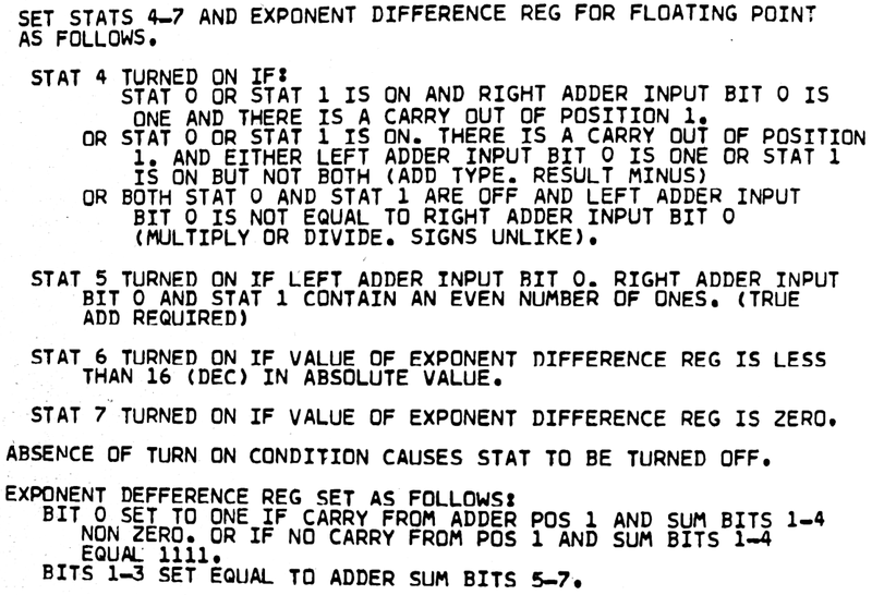
  20. The micro-operation that caused me the most difficulty is ED*FP, which computes the difference between two exponents for floating-point, but also computes four floating-point flags including the sign depending on the type of operation. Not only is this operation complex, but I think there is a typo in the description.

    A description of the ED*FP micro-operation.

    A description of the ED*FP micro-operation.

    Another complex micro-operation is MLJK, which performs multiple actions as part of instruction decoding:

    Gate adder latch to L reg and M reg. Gate latch bits 12-15 to J reg. Gate latch bits 16-19 to MD counter. Turn off refetch stat.
    If latch bits 12-15 all zero, turn on stat 0. Otherwise turn off stat 0.
    If latch bits 16-19 all zero, turn on stat 1. Otherwise turn off stat 1.
    If latch bits 16-17 all zero, turn on one-syllable stat. Otherwise turn off one-syllable stat.
    If latch bits 0-1 equal 00, set ILC to 01.
    If latch bits 0-1 equal 01 or 10, set ILC to 10.
    If latch bits 0-1 equal 11, set ILC to 11.