Showing posts sorted by date for query i960. Sort by relevance Show all posts

Examining the silicon dies of the Intel 386 processor

You might think of the Intel 386 processor (1985) as just an early processor in the x86 line, but the 386 was a critical turning point for modern computing in several ways.1 First, the 386 moved the x86 architecture to 32 bits, defining the dominant computing architecture for the rest of the 20th century. The 386 also established the overwhelming importance of x86, not just for Intel, but for the entire computer industry. Finally, the 386 ended IBM's control over the PC market, turning Compaq into the architectural leader.

In this blog post, I look at die photos of the Intel 386 processor and explain what they reveal about the history of the processor, such as the move from the 1.5 µm process to the 1 µm process. You might expect that Intel simply made the same 386 chip at a smaller scale, but there were substantial changes to the chip's layout, even some visible to the naked eye.2 I also look at why the 386 SL had over three times the transistors as the other 386 versions.3

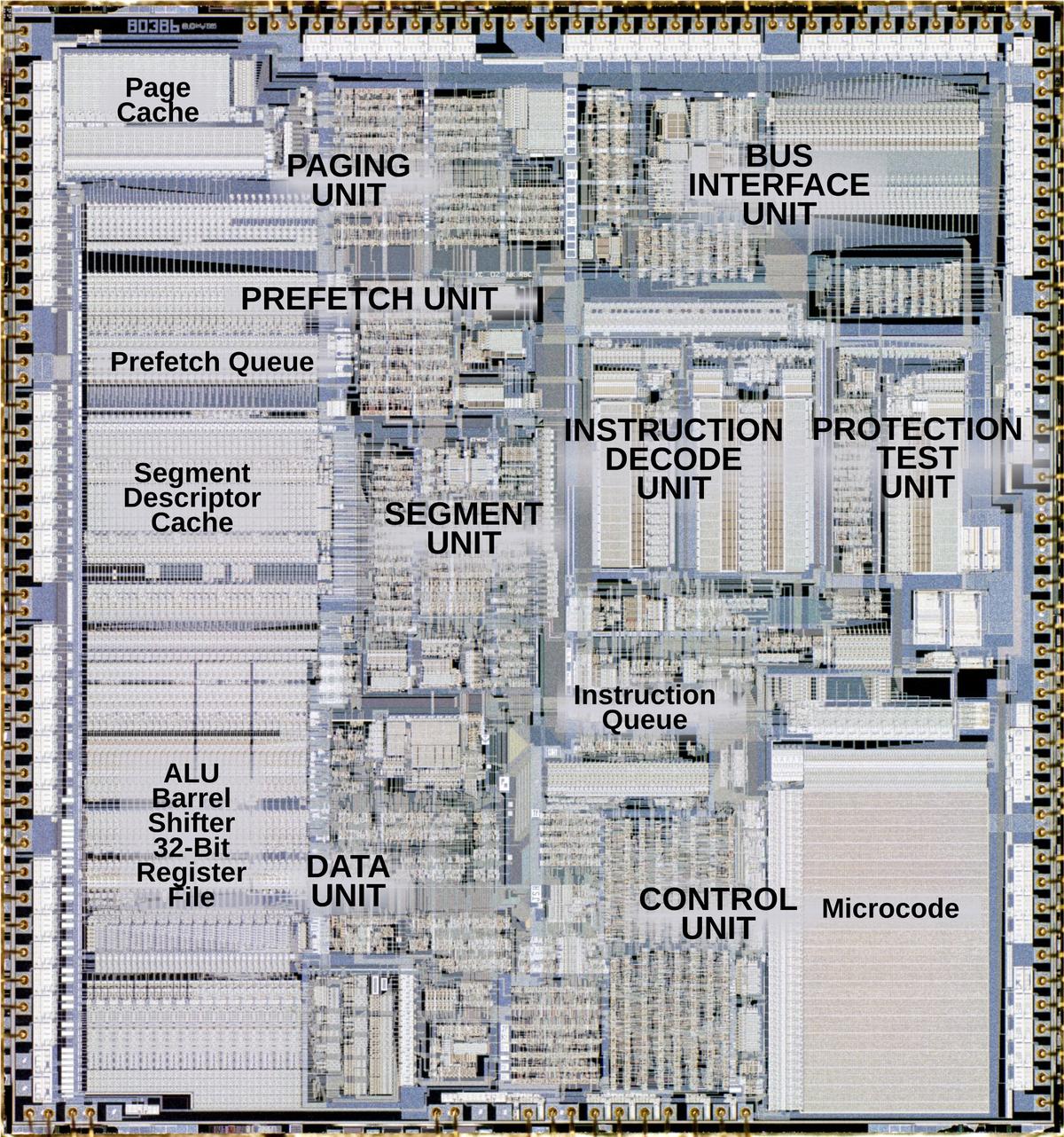
The 80386 was a major advancement over the 286: it implemented a 32-bit architecture, added more instructions, and supported 4-gigabyte segments. The 386 is a complicated processor (by 1980s standards), with 285,000 transistors, ten times the number of the original 8086.4 The 386 has eight logical units that are pipelined5 and operate mostly autonomously.6 The diagram below shows the internal structure of the 386.7

The 386 with the main functional blocks labeled. Click this image (or any other) for a larger version. I created this image using a die photo from Antoine Bercovici.

The 386 with the main functional blocks labeled. Click this image (or any other) for a larger version. I created this image using a die photo from Antoine Bercovici.

The heart of a processor is the datapath, the components that hold and process data. In the 386, these components are in the lower left: the ALU (Arithmetic/Logic Unit), a barrel shifter to shift data, and the registers. These components form regular rectangular blocks, 32 bits wide. The datapath, along with the circuitry to the left that manages it, forms the Data Unit. In the lower right is the microcode ROM, which breaks down machine instructions into micro-instructions, the low-level steps of the instruction. The microcode ROM, along with the microcode engine circuitry, forms the Control Unit.

The 386 has a complicated instruction format. The Instruction Decode Unit breaks apart an instruction into its component parts and generates a pointer to the microcode that implements the instruction. The instruction queue holds three decoded instructions. To improve performance, the Prefetch Unit reads instructions from memory before they are needed, and stores them in the 16-byte prefetch queue.8

The 386 implements segmented memory and virtual memory, with access protection.9 The Memory Management Unit consists of the Segment Unit and the Paging Unit: the Segment Unit translates a logical address to a linear address, while the Paging Unit translates the linear address to a physical address. The segment descriptor cache and page cache (TLB) hold data about segments and pages; the 386 has no on-chip instruction or data cache.10 The Bus Interface Unit in the upper right handles communication between the 386 and the external memory and devices.

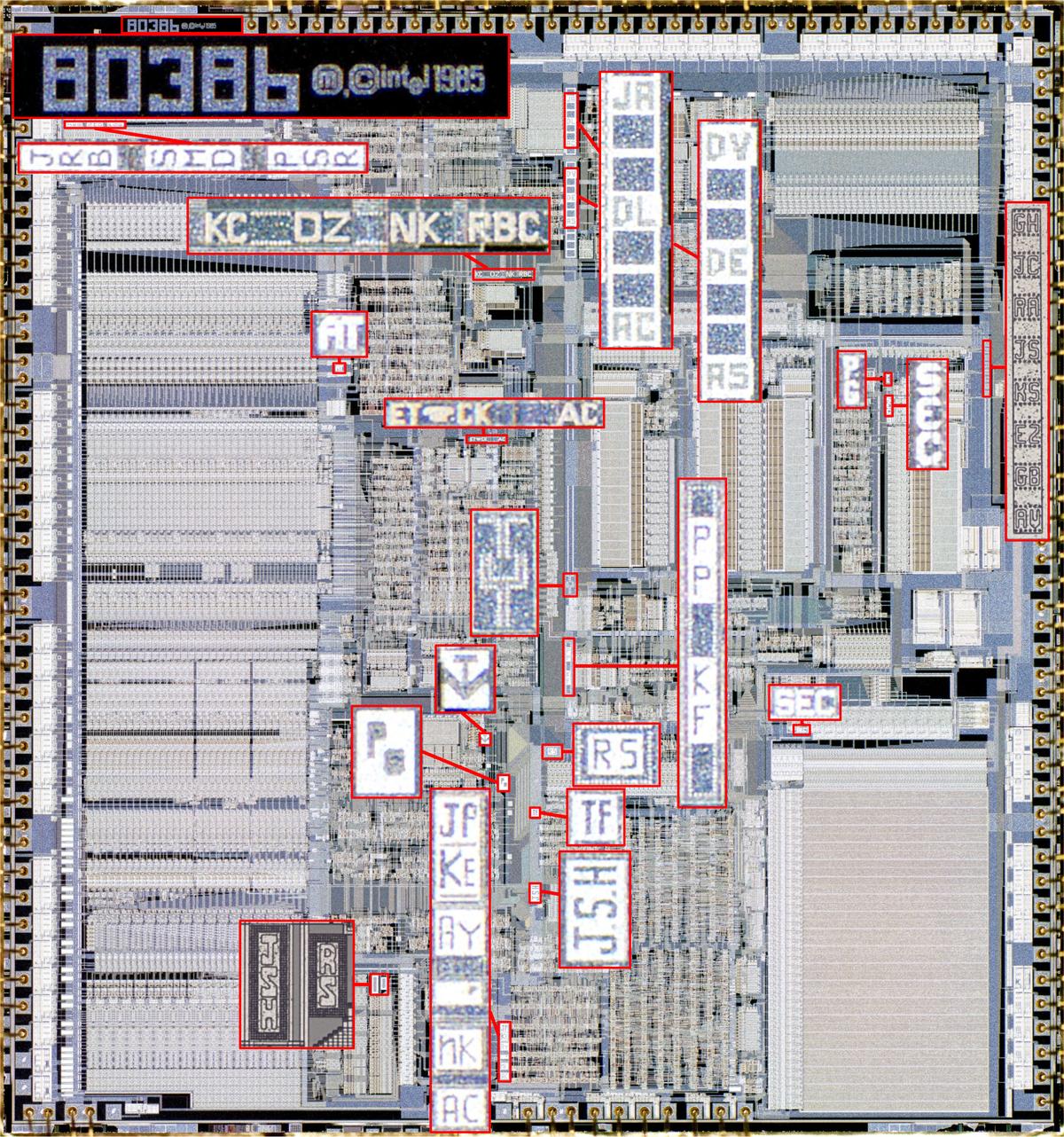
Silicon dies are often labeled with the initials of the designers. The 386 DX, however, has an unusually large number of initials. In the image below, I have enlarged the tiny initials so they are visible. I think the designers put their initials next to the unit they worked on, but I haven't been able to identify most of the names.11

The 386 die with the initials magnified.

The 386 die with the initials magnified.

The shrink from 1.5 µm to 1 µm

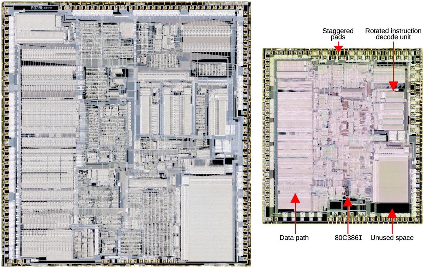
The original 386 was built on a process called CHMOS-III that had 1.5 µm features (specifically the gate channel length for a transistor). Around 1987, Intel moved to an improved process called CHMOS-IV, with 1 µm features, permitting a considerably smaller die for the 386. However, shrinking the layout wasn't a simple mechanical process. Instead, many changes were made to the chip, as shown in the comparison diagram below. Most visibly, the Instruction Decode Unit and the Protection Unit in the center-right are horizontal in the smaller die, rather than vertical. The standard-cell logic (discussed later) is considerably more dense, probably due to improved layout algorithms. The data path (left) was highly optimized in the original so it remained essentially unchanged, but smaller. One complication is that the bond pads around the border needed to remain the same size so bond wires could be attached. To fit the pads around the smaller die, many of the pads are staggered. Because different parts of the die shrank differently, the blocks no longer fit together as compactly, creating wasted space at the bottom of the die. For some reason, the numerous initials on the original 386 die were removed. Finally, the new die was labeled 80C386I with a copyright date of 1985, 1987; it is unclear what "C" and "I" indicate.

Comparison of the 1.5 µm die and the 1 µm die at the same scale. Photos courtesy of Antoine Bercovici.

Comparison of the 1.5 µm die and the 1 µm die at the same scale. Photos courtesy of Antoine Bercovici.

The change from 1.5 µm to 1 µm may not sound significant, but it reduced the die size by 60%. This allowed more dies on a wafer, substantially dropping the manufacturing cost.12 The strategy of shrinking a processor to a new process before designing a new microarchitecture for the process became Intel's tick-tock strategy.

The 386 SX

In 1988, Intel introduced the 386 SX processor, the low-cost version of the 386, with a 16-bit bus instead of a 32-bit bus. (This is reminiscent of the 8088 processor with an 8-bit bus versus the 8086 processor with a 16-bit bus.) According to the 386 oral history, the cost of the original 386 die decreased to the point where the chip's package cost about as much as the die. By reducing the number of pins, the 386 SX could be put in a one-dollar plastic package and sold for a considerably reduced price. The SX allowed Intel to segment the market, moving low-end customers from the 286 to the 386 SX, while preserving the higher sales price of the original 386, now called the DX.13 In 1988, Intel sold the 386 SX for $219, at least $100 less than the 386 DX. A complete SX computer could be $1000 cheaper than a similar DX model.

For compatibility with older 16-bit peripherals, the original 386 was designed to support a mixture of 16-bit and 32-bit buses, dynamically switching on a cycle-by-cycle basis if needed. Because 16-bit support was built into the 386, the 386 SX didn't require much design work. (Unlike the 8088, which required a redesign of the 8086's bus interface unit.)

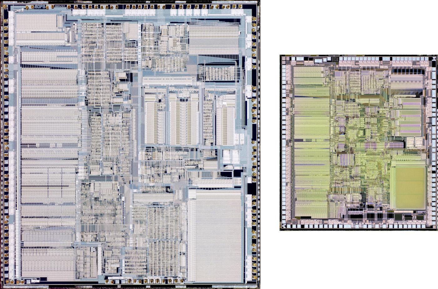
The 386 SX was built at both 1.5 µm and 1 µm. The diagram below compares the two sizes of the 386 SX die. These photos may look identical to the 386 DX photos in the previous section, but close examination shows a few differences. Since the 386 SX uses fewer pins, it has fewer bond pads, eliminating the staggered pads of the shrunk 386 DX. There are a few differences at the bottom of the chip, with wiring in much of the 386 DX's wasted space.

Comparison of two dies for the 386 SX. Photos courtesy of Antoine Bercovici.

Comparison of two dies for the 386 SX. Photos courtesy of Antoine Bercovici.

Comparing the two SX revisions, the larger die is labeled "80P9"; Intel's internal name for the chip was "P9", using their confusing series of P numbers. The shrunk die is labeled "80386SX", which makes more sense. The larger die is copyright 1985, 1987, while the shrunk die (which should be newer) is copyright 1985 for some reason. The larger die has mostly the same initials as the DX, with a few changes. The shrunk die has about 21 sets of initials.

The 386 SL die

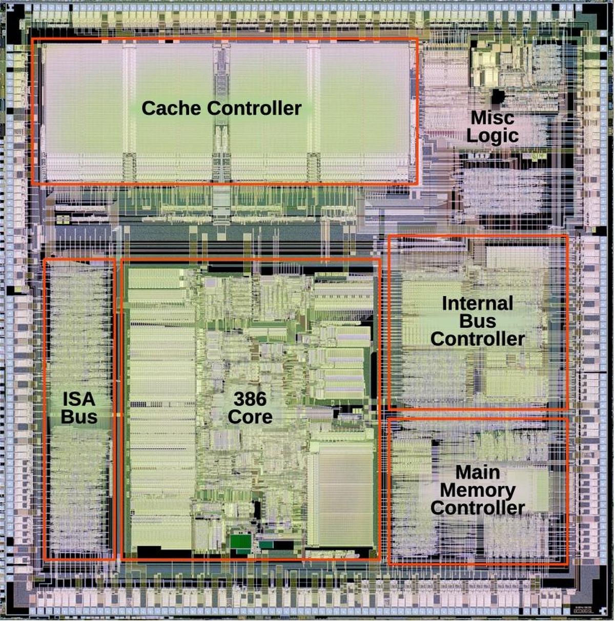
The 386 SL (1990) was a major extension to the 386, combining a 386 core and other functions on one chip to save power and space. Named "SuperSet", it was designed to corner the notebook PC market.14 The 386 SL chip included an ISA bus controller, power management logic, a cache controller for an external cache, and the main memory controller.

Looking at the die photo below, the 386 core itself takes up about 1/4 of the SL's die. The 386 core is very close to the standard 386 DX, but there are a few visible differences. Most visibly, the bond pads and pin drivers have been removed from the core. There are also some circuitry changes. For instance, the 386 SL core supports the System Management Mode, which suspends normal execution, allowing power management and other low-level hardware tasks to be performed outside the regular operating system. System Management Mode is now a standard part of the x86 line, but it was introduced in the 386 SL.

The 386 SL die with functional blocks labeled.  Die photo courtesy of Antoine Bercovici.

The 386 SL die with functional blocks labeled. Die photo courtesy of Antoine Bercovici.

In total, the 386 SL contains 855,000 transistors,15 over 3 times as many as the regular 386 DX. The cache tag RAM takes up a lot of space and transistors. The cache data itself is external; this on-chip circuitry just manages the cache. The other new components are largely implemented with standard-cell logic (discussed below); this is visible as uniform stripes of circuitry, most clearly in the ISA bus controller.

A brief history of the 386

From the modern perspective, it seems obvious for Intel to extend the x86 line from the 286 to the 386, while keeping backward compatibility. But at the time, this path was anything but clear. This history starts in the late 1970s, when Intel decided to build a "micromainframe" processor, an advanced 32-bit processor for object-oriented programming that had objects, interprocess communication, and memory protection implemented in the CPU. This overly ambitious project fell behind schedule, so Intel created a stopgap processor to sell until the micromainframe processor was ready. This stopgap processor was the 16-bit 8086 processor (1978).

In 1981, IBM decided to use the Intel 8088 (an 8086 variant) in the IBM Personal Computer (PC), but Intel did not realize the importance of this at the time. Instead, Intel was focused on their micromainframe processor, also released in 1981 as the iAPX 432, but this became "one of the great disaster stories of modern computing" as the New York Times called it. Intel then reimplemented the ideas of the ill-fated iAPX 432 on top of a RISC architecture, creating the more successful i960.

Meanwhile, things weren't going well at first for the 286 processor, the follow-on to the 808616. Bill Gates and others called its design "brain-damaged". IBM was unenthusiastic about the 286 for their own reasons.17 As a result, the 386 project was a low priority for Intel and the 386 team felt that it was the "stepchild"; internally, the 386 was pitched as another stopgap, not Intel's "official" 32-bit processor.

Despite the lack of corporate enthusiasm, the 386 team came up with two proposals to extend the 286 to a 32-bit architecture. The first was a minimal approach to extend the existing registers and address space to 32 bits. The more ambitious proposal would add more registers and create a 32-bit instruction set that was significantly different from the 8086's 16-bit instruction set. At the time, the IBM PC was still relatively new, so the importance of the installed base of software wasn't obvious; software compatibility was viewed as a "nice to have" feature rather than essential. After much debate, the decision was made around the end of 1982 to go with the minimal proposal, but supporting both segments and flat addressing, while keeping compatibility with the 286.

By 1984, though, the PC industry was booming and the 286 was proving to be a success. This produced enormous political benefits for the 386 team, who saw the project change from "stepchild" to "king". Intel introduced the 386 in 1985, which was otherwise "a miserable year for Intel and the rest of the semiconductor industry," as Intel's annual report put it. Due to an industry-wide business slowdown, Intel's net income "essentially disappeared." Moreover, facing heavy competition from Japan, Intel dropped out of the DRAM business, a crushing blow for a company that got its start in the memory industry. Fortunately, the 386 would change everything.

Given IBM's success with the IBM PC, Intel was puzzled that IBM wasn't interested in the 386 processor, but IBM had a strategy of their own.18 By this time, the IBM PC was being cloned by many competitors, but IBM had a plan to regain control of the PC architecture and thus the market: in 1987, IBM introduced the PS/2 line. These new computers ran the OS/2 operating system instead of Windows and used the proprietary Micro Channel architecture.19 IBM used multiple engineering and legal strategies to make cloning the PS/2 slow, expensive, and risky, so IBM expected they could take back the market from the clones.

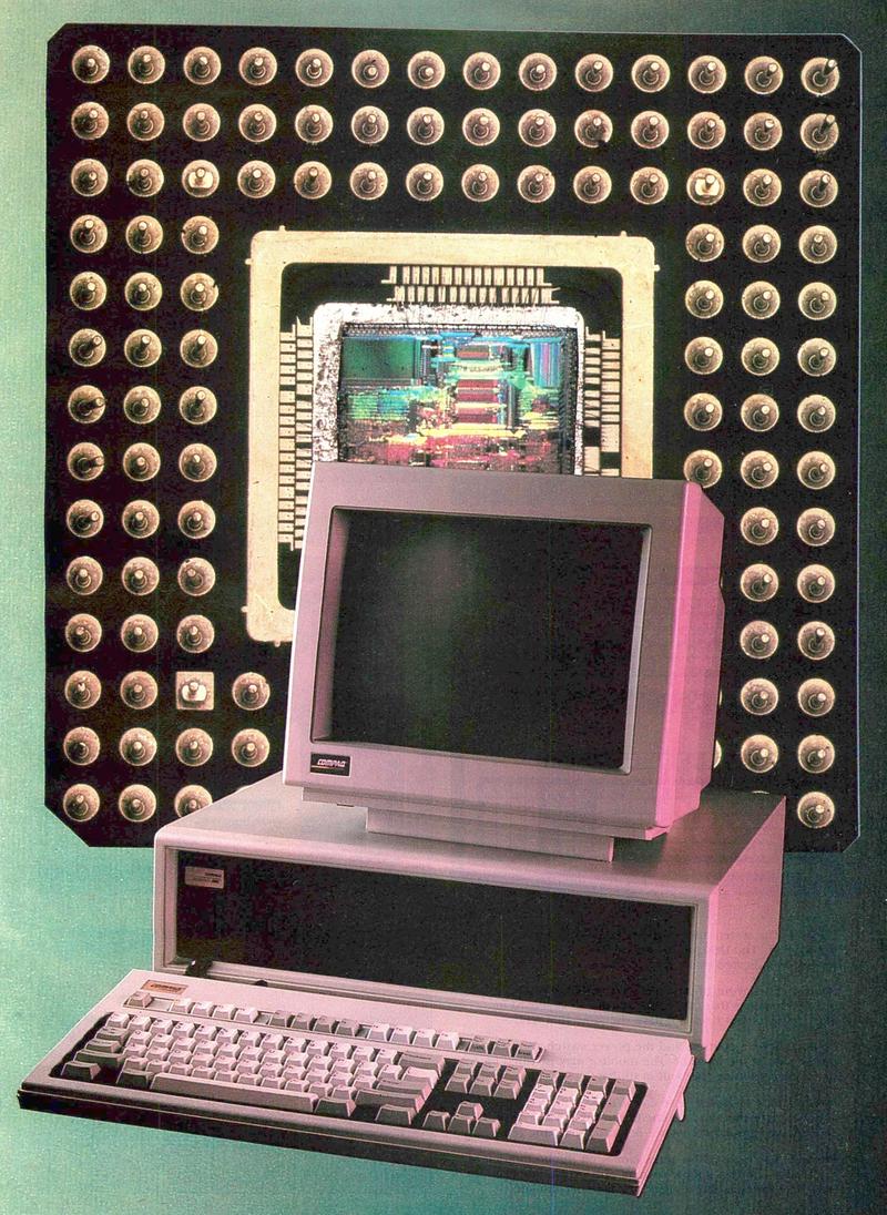
Compaq took the risky approach of ignoring IBM and following their own architectural direction.20 Compaq introduced the high-end Deskpro 386 line in September 1986, becoming the first major company to build 386-based computers. An "executive" system, the Deskpro 386 model 40 had a 40-megabyte hard drive and sold for $6449 (over $15,000 in current dollars). Compaq's gamble paid off and the Deskpro 386 was a rousing success.

The Compaq Deskpro 386 in front of the 386 processor (not to scale). From PC Tech Journal, 1987. Curiously, the die image of the 386 has been mirrored, as can be seen both from the positions of the microcode ROM and instruction decoder at the top as well as from the position of the cut corner of the package.

The Compaq Deskpro 386 in front of the 386 processor (not to scale). From PC Tech Journal, 1987. Curiously, the die image of the 386 has been mirrored, as can be seen both from the positions of the microcode ROM and instruction decoder at the top as well as from the position of the cut corner of the package.

As for IBM, the PS/2 line was largely unsuccessful and failed to become the standard. Rather than regaining control over the PC, "IBM lost control of the PC standard in 1987 when it introduced its PS/2 line of systems."21 IBM exited the PC market in 2004, selling the business to Lenovo. One slightly hyperbolic book title summed it up: "Compaq Ended IBM's PC Domination and Helped Invent Modern Computing". The 386 was a huge moneymaker for Intel, leading to Intel's first billion-dollar quarter in 1990. It cemented the importance of the x86 architecture, not just for Intel but for the entire computing industry, dominating the market up to the present day.22

How the 386 was designed

The design process of the 386 is interesting because it illustrates Intel's migration to automated design systems and heavier use of simulation.23 At the time, Intel was behind the industry in its use of tools so the leaders of the 386 realized that more automation would be necessary to build a complex chip like the 386 on schedule. By making a large investment in automated tools, the 386 team completed the design ahead of schedule. Along with proprietary CAD tools, the team made heavy use of standard Unix tools such as sed, awk, grep, and make to manage the various design databases.

The 386 posed new design challenges compared to the previous 286 processor. The 386 was much more complex, with twice the transistors. But the 386 also used fundamentally different circuitry. While the 286 and earlier processors were built from NMOS transistors, the 386 moved to CMOS (the technology still used today). Intel's CMOS process was called CHMOS-III (complementary high-performance metal-oxide-silicon) and had a feature size of 1.5 µm. CHMOS-III was based on Intel's HMOS-III process (used for the 286), but extended to CMOS. Moreover, the CHMOS process provided two layers of metal instead of one, changing how signals were routed on the chip and requiring new design techniques.

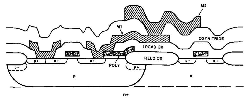
The diagram below shows a cross-section through a CHMOS-III circuit, with an NMOS transistor on the left and a PMOS transistor on the right. Note the jagged three-dimensional topography that is formed as layers cross each other (unlike modern polished wafers). This resulted in the "forbidden gap" problem that caused difficulty for the 386 team. Specifically second-layer metal (M2) could be close to the first-layer metal (M1) or it could be far apart, but an in-between distance would cause problems: the forbidden gap. If the metal layer crossed in the "forbidden gap", the metal could crack and whiskers of metal would touch, causing the chip to fail. These problems reduced the yield of the 386.

A cross-section of circuitry formed with the CHMOS-III process. From A double layer metal CHMOS III technology.

A cross-section of circuitry formed with the CHMOS-III process. From A double layer metal CHMOS III technology.

The design of the 386 proceeded both top-down, starting with the architecture definition, and bottom-up, designing standard cells and other basic circuits at the transistor level. The processor's microcode, the software that controlled the chip, was a fundamental component. It was designed with two CAD tools: an assembler and microcode rule checker. The high-level design of the chip (register-level RTL) was created and refined until clock-by-clock and phase-by-phase timing were represented. The RTL was programmed in MAINSAIL, a portable Algol-like language based on SAIL (Stanford Artificial Intelligence Language). Intel used a proprietary simulator called Microsim to simulate the RTL, stating that full-chip RTL simulation was "the single most important simulation model of the 80386".

The next step was to convert this high-level design into a detailed logic design, specifying the gates and other circuitry using Eden, a proprietary schematics-capture system. Simulating the logic design required a dedicated IBM 3083 mainframe that compared it against the RTL simulations. Next, the circuit design phase created the transistor-level design. The chip layout was performed on Applicon and Eden graphics systems. The layout started with critical blocks such as the ALU and barrel shifter. To meet the performance requirements, the TLB (translation lookaside buffer) for the paging mechanism required a creative design, as did the binary adders.

Examples of standard cells used in the 386. From "Automatic Place and Route Used on the 80386" by Joseph Krauskopf and Pat Gelsinger. I have added color.

Examples of standard cells used in the 386. From "Automatic Place and Route Used on the 80386" by Joseph Krauskopf and Pat Gelsinger, Intel Technology Journal spring 1986. I have added color.

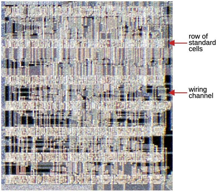
The "random" (unstructured) logic was implemented with standard cells, rather than the transistor-by-transistor design of earlier processors. The idea of standard cells is to have fixed blocks of circuitry (above) for logic gates, flip-flops, and other basic functions.24 These cells are arranged in rows by software to implement the specified logic description. The space between the rows is used as a wiring channel for connections between the cells. The disadvantage of a standard cell layout is that it generally takes up more space than an optimized hand-drawn layout, but it is much faster to create and easier to modify.

These standard cells are visible in the die as regular rows of circuitry. Intel used the TimberWolf automatic placement and routing package, which used simulated annealing to optimize the placement of cells. TimberWolf was built by a Berkeley grad student; one 386 engineer said, "If management had known that we were using a tool by some grad student as the key part of the methodology, they would never have let us use it. " Automated layout was a new thing at Intel; using it improved the schedule, but the lower density raised the risk that the chip would be too large.

Standard cells in the 386. Each row consists of numerous standard cells packed together. Each cell is a simple circuit such as a logic gate or flip flop. The wide wiring channels between the rows hold the wiring that connects the cells. This block of circuitry is in the bottom center of the chip.

Standard cells in the 386. Each row consists of numerous standard cells packed together. Each cell is a simple circuit such as a logic gate or flip flop. The wide wiring channels between the rows hold the wiring that connects the cells. This block of circuitry is in the bottom center of the chip.

The data path consists of the registers, ALU (Arithmetic Logic Unit), barrel shifter, and multiply/divide unit that process the 32-bit data. Because the data path is critical to the performance of the system, it was laid out by hand using a CALMA system. The designers could optimize the layout, taking advantage of regularities in the circuitry, optimizing the shape and size of each transistor and fitting them together like puzzle pieces. The data path is visible on the left side of the die, forming orderly 32-bit-wide rectangles in contrast to the tangles of logic next to it.

Once the transistor-level layout was complete, Intel's Hierarchical Connectivity Verification System checked that the final layout matched the schematics and adhered to the process design rules. The 386 set an Intel speed record, taking just 11 days from completing the layout to "tapeout", when the chip data is sent on magnetic tape to the mask fabrication company. (The tapeout team was led by Pat Gelsinger, who later became CEO of Intel.) After the glass masks were created using an electron-beam process, Intel's "Fab 3" in Livermore (the first to wear the bunnysuits) produced the 386 silicon wafers.

Chip designers like to claim that their chip worked the first time, but that was not the case for the 386. When the team received the first silicon for the 386, they ran a trivial do-nothing test program, "NoOp, NoOp, Halt", and it failed. Fortunately, they found a small fix to a PLA (Programmable Logic Array). Rather than create new masks, they were able to patch the existing mask with ion milling and get new wafers quickly. These wafers worked well enough that they could start the long cycles of debugging and fixing.

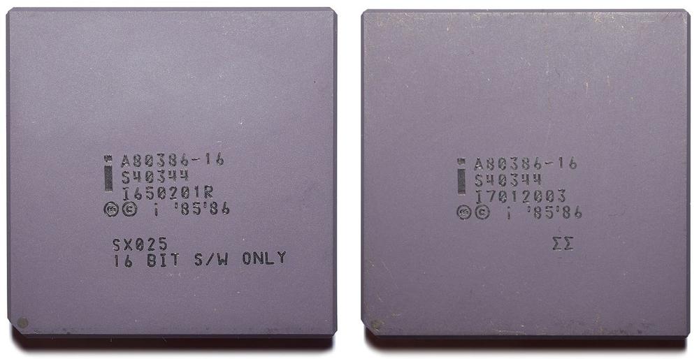
Once the processor was released, the problems weren't over.25 Some early 386 processors had a 32-bit multiply problem, where some arguments would unpredictably produce the wrong results under particular temperature/voltage/frequency conditions. (This is unrelated to the famous Pentium FDIV bug that cost Intel $475 million.) The root cause was a layout problem, not a logic problem; they didn't allow enough margin to handle the worst case data in combination with manufacturing process and environment factors. This tricky problem didn't show up in simulation or chip verification, but was only found in stress testing. Intel sold the faulty processors, but marked them as only valid for 16-bit software, while marking the good processors with a double sigma, as seen below.26 This led to embarrassing headlines such as Some 386 Systems Won't Run 32-Bit Software, Intel Says. The multiply bug also caused a shortage of 386 chips in 1987 and 1988 as Intel redesigned the chip to fix the bug. Overall, the 386 issues probably weren't any worse than other processors and the problems were soon forgotten.

Bad and good versions of the 386. Note the labels on the bottom line. Photos (L), (R) by Thomas Nguyen, (CC BY-SA 4.0).

Bad and good versions of the 386. Note the labels on the bottom line. Photos (L), (R) by Thomas Nguyen, (CC BY-SA 4.0).

Conclusions

A 17-foot tall plot of the 386. The datapath is on the left and the microcode is in the lower right. It is unclear if this is engineering work or an exhibit at MOMA. Image spliced together from the 1985 annual report.

A 17-foot tall plot of the 386. The datapath is on the left and the microcode is in the lower right. It is unclear if this is engineering work or an exhibit at MOMA. Image spliced together from the 1985 annual report.

The 386 processor was a key turning point for Intel. Intel's previous processors sold very well, but this was largely due to heavy marketing ("Operation Crush") and the good fortune to be selected for the IBM PC. Intel was technologically behind the competition, especially Motorola. Motorola had introduced the 68000 processor in 1979, starting a powerful line of (more-or-less) 32-bit processors. Intel, on the other hand, lagged with the "brain-damaged" 16-bit 286 processor in 1982. Intel was also slow with the transition to CMOS; Motorola had moved to CMOS in 1984 with the 68020.

The 386 provided the necessary technological boost for Intel, moving to a 32-bit architecture, transitioning to CMOS, and fixing the 286's memory model and multitasking limitations, while maintaining compatibility with the earlier x86 processors. The overwhelming success of the 386 solidified the dominance of the x86 and Intel, and put other processor manufacturers on the defensive. Compaq used the 386 to take over PC architecture leadership from IBM, leading to the success of Compaq, Dell, and other companies, while IBM eventually departed the PC market entirely. Thus, the 386 had an oversized effect on the computer industry, shaping the winners and losers for decades.

I plan to write more about the 386, so follow me on Twitter @kenshirriff or RSS for updates. I'm also on Mastodon occasionally as @[email protected]. Acknowledgements: The die photos are courtesy of Antoine Bercovici; you should follow him on Twitter as @Siliconinsid.27 Thanks to Pat Gelsinger and Roxanne Koester for providing helpful papers.

Notes and references

  1. The 386 also changed the industry because Intel abandoned the standard practice of second sourcing (allowing other companies to manufacture a chip). AMD, for example, had been a second source for the 286. But Intel decided to keep production of the 386 to themselves. Intel ended up licensing the 386 to IBM, though, as the IBM 386SLC. Despite the name, this was the 386 SX, not the 386 SL. 

  2. Intel made various keychains containing the 386 die, as shown at CPU World. If you know where to look, it is easy to distinguish the variants. In particular, look at the instruction decoders above the microcode and see if they are oriented vertically (pre-shrink 386) or horizontally (post-shrink 386). 

  3. The naming of the 386 versions is a bit of a mess. The 386 started as the 80386 and later the i386. The 80386SX was introduced in 1988; this is the version with a 16-bit bus. The "regular" 386 was then renamed the DX to distinguish it from the SX. There are several other versions of the 386 that I won't discuss here, such as the EX, CXSB, and 80376. See Wikipedia for details.

    Confusingly, the 486 also used the SX and DX names, but in a different way. The 486 DX was the original that included a floating-point unit, while floating-point was disabled in the 486 SX. Thus, in both cases "DX" was the full chip, while "SX" was the low-cost version, but the removed functionality was entirely different.

    Another complication is that a 386DX chip will have a marking like "SX217", but this has nothing to do with the 386 SX. SX217 is an Intel S-Specification number, which specifies the particular stepping of the processor, indicating a manufacturing change or if a feature has been fixed or removed. 

  4. Counting transistors isn't as straightforward as you might think. For example, a ROM may have a transistor for a 1 bit and no transistor for a 0 bit. Thus, the number of transistors depends on the data stored in the ROM. Likewise, a PLA has transistors present or absent in a grid, depending on the desired logic functions. For this reason, transistor counts are usually the number of "transistor sites", locations that could have a transistor, even if a transistor is not physically present. In the case of the 386, it has 285,000 transistor sites and 181,000 actual transistors (source), so over 100,000 reported transistors don't actually exist.

    I'll also point out that most sources claim 275,000 transistors for the 386. My assumption is that 285,000 is the more accurate number (since this source distinguishes between transistor sites and physical transistors), while 275,000 is the rounded number. 

  5. The 386's independent, pipelined functional units provide a significant performance improvement and the pipeline can be executing up to eight instructions at one time. For instance, the 386's microcode engine permits some overlap between the end of one instruction and the beginning of the next, an overlap that speeds up the processor by about 9%. But note that instructions are still executed sequentially, taking multiple clocks per instruction, so it is nothing like the superscalar execution introduced in the Pentium. 

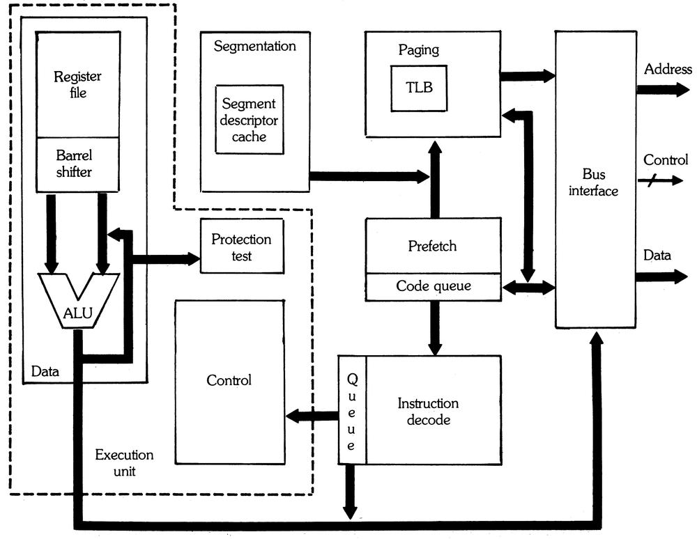
  6. The diagram of the 386 die shows eight functional units. It can be compared to the block diagram below, which shows how the units are interconnected.

    Block diagram of the 386. From The Intel 80386—Architecture and Implementation.


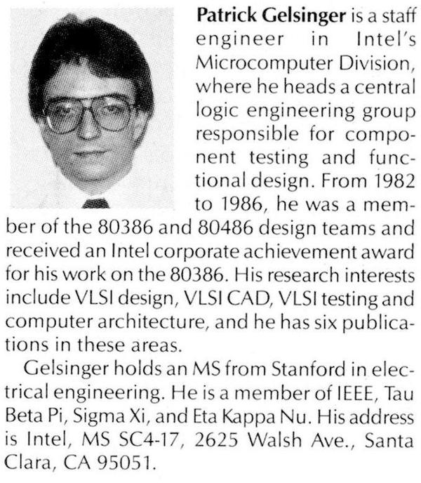
  7. My labeled die diagram combines information from two Intel papers: The Intel 80386—Architecture and Implementation and Design and Test of the 80386. The former paper describes the eight functional units. The latter paper provides more details, but only shows six functional units. (The Control Unit and Data Unit are combined into the Execution Unit, while the Protection Test Unit is dropped as an independent unit.) Interestingly, the second paper is by Patrick Gelsinger, who is now CEO of Intel. Pat Gelsinger also wrote "80386 Tapeout - Giving Birth to an Elephant", which says there are nine functional units. I don't know what the ninth unit is, maybe the substrate bias generator? In any case, the count of functional units is flexible.

    Patrick Gelsinger's biography from his 80386 paper.

    Patrick Gelsinger's biography from his 80386 paper.


  8. The 386 has a 16-byte prefetch queue, but apparently only 12 bytes are used due to a pipeline bug (details). 

  9. Static checks for access violations are performed by the Protection Test Unit, while dynamic checks are performed by the Segment Unit and the Paging Unit. 

  10. The 386 was originally supposed to have an on-chip cache, but there wasn't room and the cache was dropped in the middle of the project. As it was, the 386 die barely fit into the lithography machine's field of view. 

  11. It kind of looks like the die has the initials ET next to a telephone. Could this be a reference to the movie E.T. and its catchphrase "E.T. phone home"? "SEC" must be senior mask designer Shirley Carter. "KF" is engineer Kelly Fitzpatrick. "PSR" is probably Paul S. Ries who designed the 386's paging unit. 

  12. I think that Intel used a 6" (150mm) wafer for the 386. With a 10mm×10mm die, about 128 chips would fit on a wafer. But with a 6mm×6.5mm die, about 344 would fit on a wafer, over 2.5 times as many. (See Die per wafer estimator.) 

  13. The 286 remained popular compared to the 386, probably due to its lower price. It wasn't until 1991 that the number of 386 units sold exceeded the 286 (source). Intel's revenue for the 386 was much, much higher than for the 286 though (source). 

  14. The "SuperSet" consisted of the 386 SL along with the 82360SL peripheral I/O chip. The I/O chip contained various ISA bus peripherals, taking the place of multiple chips such as the 8259 that dated back to the 8080 processor. The I/O chip included DMA controllers, timers, interrupt controllers, a real time clock, serial ports, and a parallel port. It also had a hard disk interface, a floppy disk controller, and a keyboard controller. 

  15. The 386 SL transistor count is from the Intel Microprocessor Quick Reference Guide, which contains information on most of Intel's processors. 

  16. The 186 processor doesn't fit cleanly into the sequence of x86 processors. Specifically, the 186 is an incompatible side-branch, rather than something in the 286, 386, 486 sequence. The 186 was essentially an 8086 that included additional functionality (clock generator, interrupt controller, timers, etc.) to make it more suitable for an emedded system. The 186 was used in some personal computers, but it was incompatible with the IBM PC so it wasn't very popular. 

  17. IBM didn't want to use the 286 because they were planning to reverse-engineer the 286 and make their own version, a 16-megahertz CMOS version. This was part of IBM's plan to regain control of the PC architecture with the PS/2. Intel told IBM that "the fastest path to a 16-megahertz CMOS 286 is the 386 because it is CMOS and 16-megahertz", but IBM continued on their own 286 path. Eventually, IBM gave up and used Intel's 286 in the PS/2. 

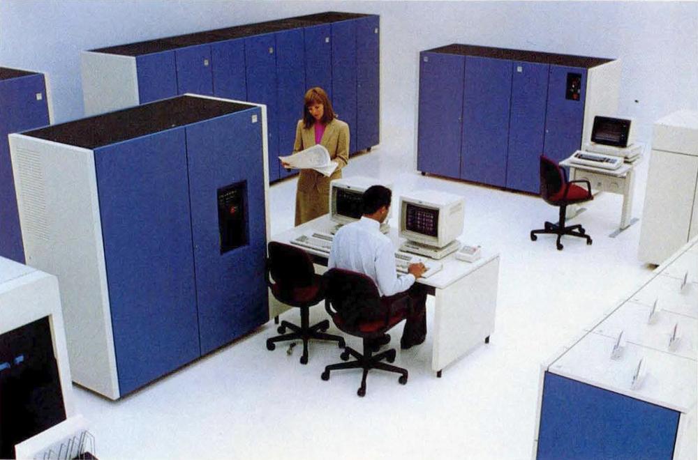
  18. IBM might have been reluctant to support the 386 processor because of the risk of cutting into sales of IBM's mid-range 4300 mainframe line. An IBM 4381-2 system ran at about 3.3 MIPS and cost $500,000, about the same MIPS performance as 386/16 system for under $10,000. The systems aren't directly comparable, of course, but many customers could use the 386 for a fraction of the price. IBM's sales of 4300 and other systems declined sharply in 1987, but the decline was blamed on DEC's VAX systems.

    An IBM 4381 system. The 4381 processor is the large cabinet to the left of the terminals. The cabinets at the back are probably IBM 3380 disk drives. From an IBM 4381 brochure.

    An IBM 4381 system. The 4381 processor is the large cabinet to the left of the terminals. The cabinets at the back are probably IBM 3380 disk drives. From an IBM 4381 brochure.


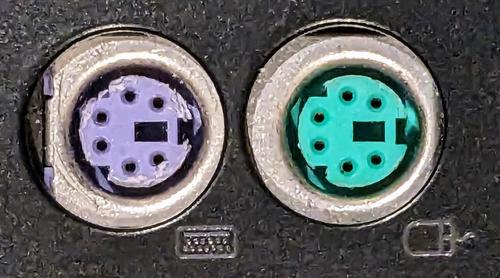
  19. The most lasting influence of the PS/2 was the round purple and green keyboard and mouse ports that were used by most PCs until USB obsoleted them. The PS2 ports are still available on some motherboards and gaming computers.

    The PS/2 keyboard and mouse ports on the back of a Gateway PC.

    The PS/2 keyboard and mouse ports on the back of a Gateway PC.


  20. When Compaq introduced their 386-based system, "they warned IBM that it has but six months to announce a similar machine or be supplanted as the market's standard setter." (source). Compaq turned out to be correct. 

  21. The quote is from Computer Structure and Logic

  22. Whenever I mention x86's domination of the computing market, people bring up ARM, but ARM has a lot more market share in people's minds than in actual numbers. One research firm says that ARM has 15% of the laptop market share in 2023, expected to increase to 25% by 2027. (Surprisingly, Apple only has 90% of the ARM laptop market.) In the server market, just an estimated 8% of CPU shipments in 2023 were ARM. See Arm-based PCs to Nearly Double Market Share by 2027 and Digitimes. (Of course, mobile phones are almost entirely ARM.) 

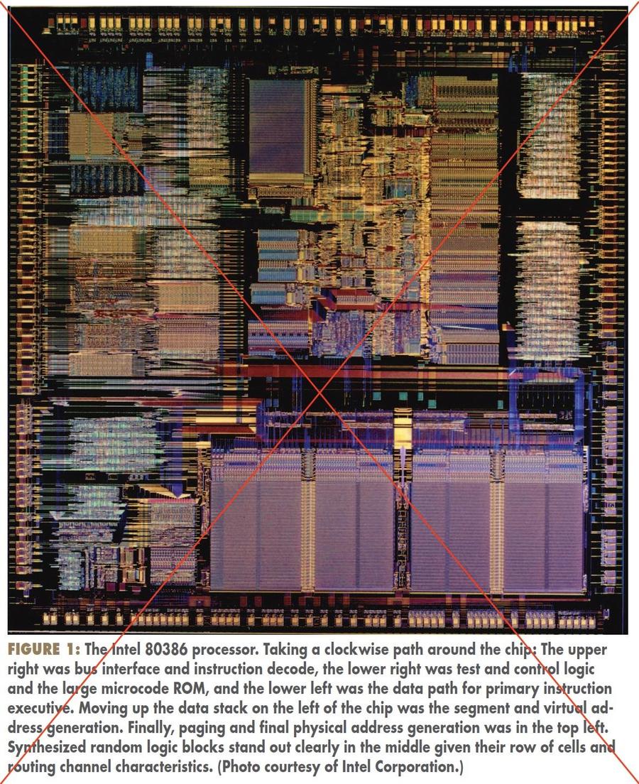
  23. Most of my section on the 386 design process is based on Design and Test of the 80386. The 386 oral history also provides information on the design process. The article Such a CAD! also describes Intel's CAD systems. Amusingly, I noticed that one of its figures (below) used a photo of the 386SL instead of the 386DX, with the result that the text is completely wrong. For instance, what it calls the microcode ROM is the cache tag RAM.

    Erroneous description of the 386 layout. I put an X through it so nobody reuses it.

    Erroneous description of the 386 layout. I put an X through it so nobody reuses it.


  24. Intel has published a guide to their 1.5 micron CHMOS III cell library. I assume this is the same standard-cell library that was used for the logic in the 386. The library provided over 150 logic functions. It also provided cell-based versions of the Intel 80C51 microcontroller and various Intel support chips such as the 82C37A DMA controller, the 82C54 interval timer, and the 82C59 interrupt controller.

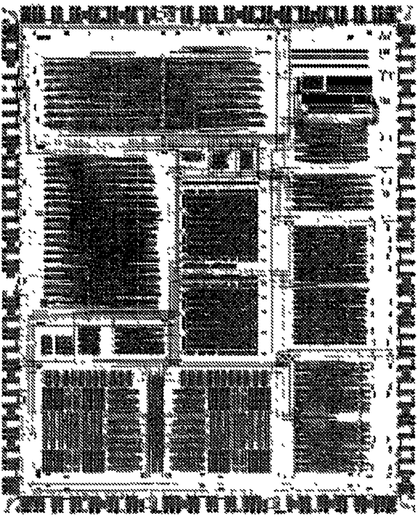
    Die photo of the 82360SL ISA Peripheral I/O Chip, from the 386 SL Data Book.

    Die photo of the 82360SL ISA Peripheral I/O Chip, from the 386 SL Data Book.

    Interestingly, the 386 SL's Peripheral I/O chip (the 82360SL) included the functionality of these support chips. Standard-cell construction is visible as the stripes in the die photo (above). Moreover, the layout of the die shows separated blocks, probably corresponding to each embedded chip. I expect that Intel designed standard-cell versions of the controller chips to embed in the I/O chip and then added the chips to the standard-cell library since they were available. 

  25. For an example of the problems that could require a new stepping of the 386, see Intel backs off 80386 claims but denies chip recast needed (1986). It discusses multitasking issues with the 386, with Intel calling them "minor imperfections" that could cause "little glitches", while others suggested that the chip would need replacement. The bugs fixed in each stepping of the 386 are documented here

  26. One curiosity about the 386 is the IBTS and XBTS instructions. The Insert Bit String and Extract Bit String instructions were implemented in the early 386 processors, but then removed in the B1 stepping. It's interesting that the bit string instructions were removed in the B1 stepping, the same stepping that fixed the 32-bit multiplication bug. Intel said that they were removed "in order to use the area of the chip previously occupied for other microcircuitry" (source). I wonder if Intel fixed the multiplication bug in microcode, and needed to discard the bit string operations to free up enough microcode space. Intel reused these opcodes in the 486 for the CMPXCHG instruction, but that caused conflicts with old 386 programs, so Intel changed the 486 opcodes in the B stepping.  

  27. Since Antoine photographed many different 386 chips, I could correlate the S-Specs with the layout changes. I'll summarize the information here, in case anyone happens to want it. The larger DX layout is associated with SX213 and SX215. (Presumably the two are different, but nothing that I could see in the photographs.) The shrunk DX layout is associated with SX217, SX218, SX366, and SX544. The 386 SL image is SX621. 

Tracing the roots of the 8086 instruction set to the Datapoint 2200 minicomputer

The Intel 8086 processor started the x86 architecture that is still extensively used today. The 8086 has some quirky characteristics: it is little-endian, has a parity flag, and uses explicit I/O instructions instead of just memory-mapped I/O. It has four 16-bit registers that can be split into 8-bit registers, but only one that can be used for memory indexing. Surprisingly, the reason for these characteristics and more is compatibility with a computer dating back before the creation of the microprocessor: the Datapoint 2200, a minicomputer with a processor built out of TTL chips. In this blog post, I'll look in detail at how the Datapoint 2200 led to the architecture of Intel's modern processors, step by step through the 8008, 8080, and 8086 processors.

The Datapoint 2200

In the late 1960s, 80-column IBM punch cards were the primary way of entering data into computers, although CRT terminals were growing in popularity. The Datapoint 2200 was designed as a low-cost terminal that could replace a keypunch, with a squat CRT display the size of a punch card. By putting some processing power into the Datapoint 2200, it could perform data validation and other tasks, making data entry more efficient. Even though the Datapoint 2200 was typically used as an intelligent terminal, it was really a desktop minicomputer with a "unique combination of powerful computer, display, and dual cassette drives." Although now mostly forgotten, the Datapoint 2200 was the origin of the 8-bit microprocessor, as I'll explain below.

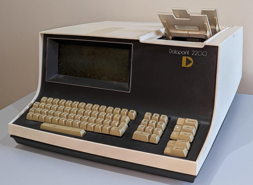
The Datapoint 2200 computer (Version II).

The Datapoint 2200 computer (Version II).

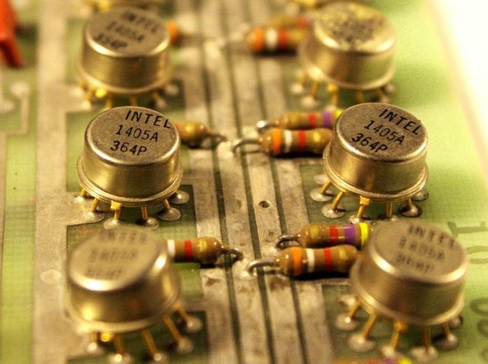
The memory storage of the Datapoint 2200 had a large impact on its architecture and thus the architecture of today's computers. In the 1960s and early 1970s, magnetic core memory was the dominant form of computer storage. It consisted of tiny ferrite rings, threaded into grids, with each ring storing one bit. Magnetic core storage was bulky and relatively expensive, though. Semiconductor RAM was new and very expensive; Intel's first product in 1969 was a RAM chip called the 3101, which held just 64 bits and cost $99.50. To minimize storage costs, the Datapoint 2200 used an alternative: MOS shift-register memory. The Intel 1405 shift-register memory chip provided much more storage than RAM chips at a much lower cost (512 bits for $13.30).1

Intel 1405 shift-register memory chips in metal cans, in the Datapoint 2200.

Intel 1405 shift-register memory chips in metal cans, in the Datapoint 2200.

The big problem with shift-register memory is that it is sequential: the bits come out one at a time, in the same order you put them in. This wasn't a problem when executing instructions sequentially, since the memory provided each instruction as it was needed. For a random access, though, you need to wait until the bits circulate around and you get the one you want, which is very slow. To minimize the number of memory accesses, the Datapoint 2200 had seven registers, a relatively large number of registers for the time.2 The registers were called A, B, C, D, E, H, and L, and these names had a lasting impact on Intel processors.

Another consequence of shift-register memory was that the Datapoint 2200 was a serial computer, operating on one bit at a time as the shift-register memory provided it, using a 1-bit ALU. To handle arithmetic operations, the ALU needed to start with the lowest bit so it could process carries. Likewise, a 16-bit value (such as a jump target) needed to start with the lowest bit. This resulted in a little-endian architecture, with the low byte first. The little-endian architecture has remained in Intel processors to the present.

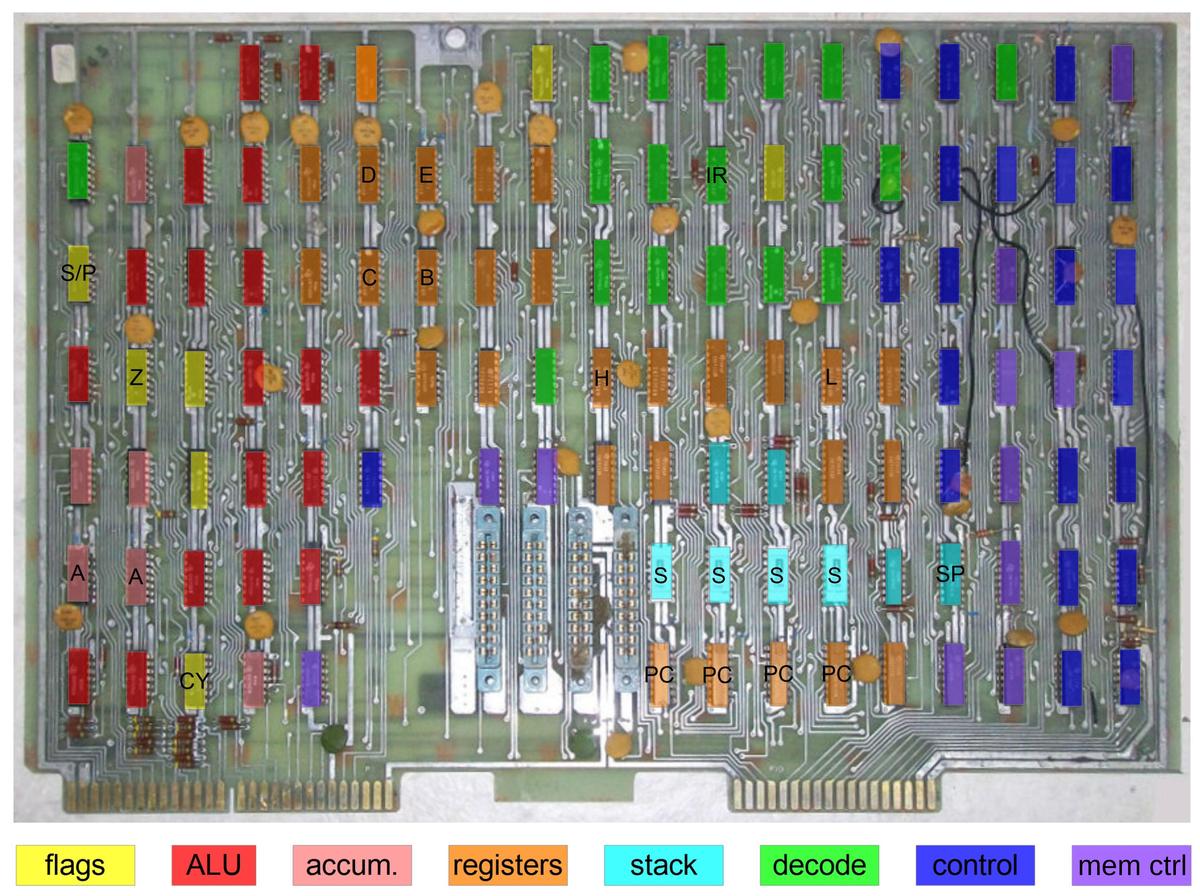
Since the Datapoint 2200 was designed before the creation of the microprocessor, its processor was built from a board of TTL chips (as was typical for minicomputers at the time). The diagram below shows the processor board with the chips categorized by function. The board has a separate chip for each 8-bit register (B, C, D, etc.) and separate chips for control flags (Z, carry, etc.). The Arithmetic/Logic Unit (ALU) takes about 18 chips, while instruction decoding is another 18 chips. Because every feature required more chips, the designers of the Datapoint 2200 were strongly motivated to make the instruction set as simple as possible. This was necessary since the Datapoint 2200 was a low-cost device, renting for just $148 a month. In contrast, the popular PDP-8 minicomputer rented for $500 a month.

The Datapoint 2200 processor board with registers, flags, and other blocks labeled. Click this image (or any other) for a larger version.

The Datapoint 2200 processor board with registers, flags, and other blocks labeled. Click this image (or any other) for a larger version.

One way that the Datapoint 2200 simplified the hardware was by creating a large set of instructions by combining simpler pieces in an orthogonal way. For instance, the Datapoint 2200 has 64 ALU instructions that apply one of eight ALU operations to one of the eight registers. This requires a small amount of hardware—eight ALU circuits and a circuit to select the register—but provides a large number of instructions. Another example is the register-to-register move instructions. Specifying one of eight source registers and one of eight destination registers provides a large, flexible set of instructions to move data.

The Datapoint 2200's instruction format was designed around this principle, with groups of three bits specifying a register. A common TTL chip could decode the group of three bits and activate the desired circuit.3 For instance, a data move instruction had the bit pattern 11DDDSSS to move a byte from the specified source (SSS) to the specified destination (DDD). (Note that this bit pattern maps onto three octal digits very nicely since the source and destination are separate digits.4)

One unusual feature of the Datapoint instruction set is that a memory access was just like a register access. That is, an instruction could specify one of the seven physical registers or could specify a memory access (M), using the identical instruction format. One consequence of this is that you couldn't include a memory address in an instruction. Instead, memory could only be accessed by first loading the address into the H and L registers, which held the high and low byte of the address respectively.5 This is very unusual and inconvenient, since a memory access took three instructions: two to load the H and L registers and one to access memory as the M "register". The advantage was that it simplified the instruction set and the decoding logic, saving chips and thus reducing the system cost. This decision also had lasting impact on Intel processors and how they access memory.

The table below shows the Datapoint 2200's instruction set in an octal table showing the 256 potential opcodes.6 I have roughly classified the instructions as arithmetic/logic (purple), control-flow (blue), data movement (green), input/output (orange), and miscellaneous (yellow). Note how the orthogonal instruction format produces large blocks of related instructions. The instructions in the lower right (green) load (L) a value from a source to a destination. (The no-operation NOP and HALT instructions are special cases.7) In the upper-left are Load operations (LA, etc.) that use an "immediate" byte, a data byte that follows the instruction. They use the same DDD code to specify the destination register, reusing that circuitry.

 0123456701234567
0HALTHALTSLCRFCAD LARETURNJFCINPUTCFC JMP CALL 
1  SRCRFZAC LB JFZ CFZ     
2   RFSSU LC JFSEX ADRCFSEX STATUS EX DATA EX WRITE
3   RFPSB LD JFPEX COM1CFPEX COM2 EX COM3 EX COM4
4   RTCND LE JTC CTC     
5   RTZXR LH JTZEX BEEPCTZEX CLICK EX DECK1 EX DECK2
6   RTSOR LL JTSEX RBKCTSEX WBK   EX BSP
7   RTPCP   JTPEX SFCTPEX SB EX REWND EX TSTOP
0ADAADBADCADDADEADHADLADMNOPLABLACLADLAELAHLALLAM
1ACAACBACCACDACEACHACLACMLBALBBLBCLBDLBELBHLBLLBM
2SUASUBSUCSUDSUESUHSULSUMLCALCBLCCLCDLCELCHLCLLCM
3SBASBBSBCSBDSBESBHSBLSBMLDALDBLDCLDDLDELDHLDLLDM
4NDANDBNDCNDDNDENDHNDLNDMLEALEBLECLEDLEELEHLELLEM
5XRAXRBXRCXRDXREXRHXRLXRMLHALHBLHCLHDLHELHHLHLLHM
6ORAORBORCORDOREORHORLORMLLALLBLLCLLDLLELLHLLLLLM
7CPACPBCPCCPDCPECPHCPLCPMLMALMBLMCLMDLMELMHLMLHALT

The lower-left quadrant (purple) has the bulk of the ALU instructions. These instructions have a regular, orthogonal structure making the instructions easy to decode: each row specifies the operation while each column specifies the source. This is due to the instruction structure: eight bits in the pattern 10AAASSS, where the AAA bits specified the ALU operation and the SSS bits specified the register source. The three-bit ALU code specifies the operations Add, Add with Carry, Subtract, Subtract with Borrow, logical AND, logical XOR, logical OR, and Compare. This list is important because it defined the fundamental ALU operations for later Intel processors.8 In the upper-left are ALU operations that use an "immediate" byte. These instructions use the same AAA bit pattern to select the ALU operation, reusing the decoding hardware. Finally, the shift instructions SLC and SRC are implemented as special cases outside the pattern.

The upper columns contain conditional instructions in blue—Return, Jump, and Call. The eight conditions test the four status flags (Carry, Zero, Sign, and Parity) for either True or False. (For example, JFZ Jumps if the Zero flag is False.) A 3-bit field selects the condition, allowing it to be easily decoded in hardware. The parity flag is somewhat unusual because parity is surprisingly expensive to compute in hardware, but because the Datapoint 2200 operated as a terminal, parity computation was important.

The Datapoint 2200 has an input instruction as well as many output instructions for a variety of specific hardware tasks (orange, labeled EX for external). Typical operations are STATUS to get I/O status, BEEP and CLICK to make sound, and REWIND to rewind the tape. As a result of this decision to use separate I/O instructions, Intel processors still use I/O instructions operating in an I/O space, different from processors such as the MOS 6502 and the Motorola 68000 that used memory-mapped I/O.

To summarize, the Datapoint 2200 has a fairly large number of instructions, but they are generated from about a dozen simple patterns that are easy to decode.9 By combining orthogonal bit fields (e.g. 8 ALU operations multiplied by 8 source registers), 64 instructions can be generated from one underlying pattern.

Intel 8008

The Intel 8008 was created as a clone of the Datapoint 2200 processor.10 Around the end of 1969, the Datapoint company talked with Intel and Texas Instruments about the possibility of replacing the processor board with a single chip. Even though the microprocessor didn't exist at this point, both companies said they could create such a chip. Texas Instruments was first with a chip called the TMX 1795 that they advertised as a "CPU on a chip". Slightly later, Intel produced the 8008 microprocessor. Both chips copied the Datapoint 2200's instruction set architecture with minor changes.

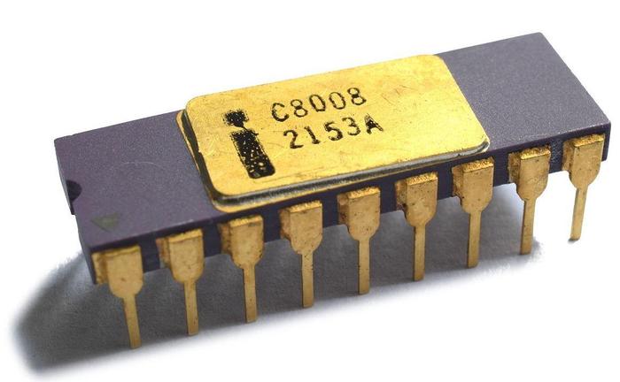
The Intel 8008 chip in its 18-pin package. The small number of pins hampered the performance of the 8008, but Intel was hesitant to even go to the 18-pin package. Photo by Thomas Nguyen, (CC BY-SA 4.0).

The Intel 8008 chip in its 18-pin package. The small number of pins hampered the performance of the 8008, but Intel was hesitant to even go to the 18-pin package. Photo by Thomas Nguyen, (CC BY-SA 4.0).

By the time the chips were completed, however, the Datapoint corporation had lost interest in the chips. They were designing a much faster version of the Datapoint 2200 with improved TTL chips (including the well-known 74181 ALU chip). Even the original Datapoint 2200 model was faster than the Intel 8008 processor, and the Version II was over 5 times faster,11 so moving to a single-chip processor would be a step backward.

Texas Instruments unsuccessfully tried to find a customer for their TMX 1795 chip and ended up abandoning the chip. Intel, however, marketed the 8008 as an 8-bit microprocessor, essentially creating the microprocessor industry. In my view, Intel's biggest innovation with the microprocessor wasn't creating a single-chip CPU, but creating the microprocessor as a product category: a general-purpose processor along with everything customers needed to take advantage of it. Intel put an enormous amount of effort into making microprocessors a success: from documentation and customer training to Intellec development systems, from support chips to software tools such as assemblers, compilers, and operating systems.

The table below shows the opcodes of the 8008. For the most part, the 8008 copies the Datapoint 2200, with identical instructions that have identical opcodes (in color). There are a few additional instructions (shown in white), though. Intel Designer Ted Hoff realized that increment and decrement instructions (IN and DC) would be very useful for loops. There are two additional bit rotate instructions (RAL and RAR) as well as the "missing" LMI (Load Immediate to Memory) instruction. The RST (restart) instructions act as short call instructions to fixed addresses for interrupt handling. Finally, the 8008 turned the Datapoint 2200's device-specific I/O instructions into 32 generic I/O instructions.

 0123456701234567
0HLTHLTRLCRFCADIRST 0LAIRETJFCINP 0CFCINP 1JMPINP 2CALINP 3
1INBDCBRRCRFZACIRST 1LBI JFZINP 4CFZINP 5 INP 6 INP 7
2INCDCCRALRFSSUIRST 2LCI JFSOUT 8CFSOUT 9 OUT 10 OUT 11
3INDDCDRARRFPSBIRST 3LDI JFPOUT 12CFPOUT 13 OUT 14 OUT 15
4INEDCE RTCNDIRST 4LEI JTCOUT 16CTCOUT 17 OUT 18 OUT 19
5INHDCH RTZXRIRST 5LHI JTZOUT 20CTZOUT 21 OUT 22 OUT 23
6INLDCL RTSORIRST 6LLI JTSOUT 24CTSOUT 25 OUT 26 OUT 27
7   RTPCPIRST 7LMI JTPOUT 28CTPOUT 29 OUT 30 OUT 31
0ADAADBADCADDADEADHADLADMNOPLABLACLADLAELAHLALLAM
1ACAACBACCACDACEACHACLACMLBALBBLBCLBDLBELBHLBLLBM
2SUASUBSUCSUDSUESUHSULSUMLCALCBLCCLCDLCELCHLCLLCM
3SBASBBSBCSBDSBESBHSBLSBMLDALDBLDCLDDLDELDHLDLLDM
4NDANDBNDCNDDNDENDHNDLNDMLEALEBLECLEDLEELEHLELLEM
5XRAXRBXRCXRDXREXRHXRLXRMLHALHBLHCLHDLHELHHLHLLHM
6ORAORBORCORDOREORHORLORMLLALLBLLCLLDLLELLHLLLLLM
7CPACPBCPCCPDCPECPHCPLCPMLMALMBLMCLMDLMELMHLMLHLT

Intel 8080

The 8080 improved the 8008 in many ways, focusing on speed and ease of use, and resolving customer issues with the 8008.12 Customers had criticized the 8008 for its small memory capacity, low speed, and difficult hardware interfacing. The 8080 increased memory capacity from 16K to 64K and was over an order of magnitude faster than the 8008. The 8080 also moved to a 40-pin package that made interfacing easier, but the 8080 still required a large number of support chips to build a working system.

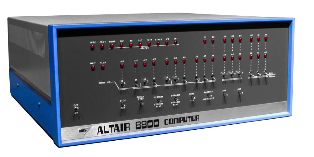
Although the 8080 was widely used in embedded systems, it is more famous for its use in the first generation of home computers, boxes such as the Altair and IMSAI. Famed chip designer Federico Faggin said that the 8080 really created the microprocessor; the 4004 and 8008 suggested it, but the 8080 made it real.13

Altair 8800 computer on display at the Smithsonian. Photo by Colin Douglas, (CC BY-SA 2.0).

Altair 8800 computer on display at the Smithsonian. Photo by Colin Douglas, (CC BY-SA 2.0).

The table below shows the instruction set for the 8080. The 8080 was designed to be compatible with 8008 assembly programs after a simple translation process; the instructions have been shifted around and the names have changed.15 The instructions from the Datapoint 2200 (colored) form the majority of the 8080's instruction set. The instruction set was expanded by adding some 16-bit support, allowing register pairs (BC, DE, HL) to be used as 16-bit registers for double add, 16-bit increment and decrement, and 16-bit memory transfers. Many of the new instructions in the 8080 may seem like contrived special cases— for example, SPHL (Load SP from HL) and XCHG (Exchange DE and HL)— but they made accesses to memory easier. The I/O instructions from the 8008 have been condensed to just IN and OUT, opening up room for new instructions.

 0123456701234567
0NOPLXI BSTAX BINX BINR BDCR BMVI BRLCMOV B,BMOV B,CMOV B,DMOV B,EMOV B,HMOV B,LMOV B,MMOV B,A
1 DAD BLDAX BDCX BINR CDCR CMVI CRRCMOV C,BMOV C,CMOV C,DMOV C,EMOV C,HMOV C,LMOV C,MMOV C,A
2 LXI DSTAX DINX DINR DDCR DMVI DRALMOV D,BMOV D,CMOV D,DMOV D,EMOV D,HMOV D,LMOV D,MMOV D,A
3 DAD DLDAX DDCX DINR EDCR EMVI ERARMOV E,BMOV E,CMOV E,DMOV E,EMOV E,HMOV E,LMOV E,MMOV E,A
4 LXI HSHLDINX HINR HDCR HMVI HDAAMOV H,BMOV H,CMOV H,DMOV H,EMOV H,HMOV H,LMOV H,MMOV H,A
5 DAD HLHLDDCX HINR LDCR LMVI LCMAMOV L,BMOV L,CMOV L,DMOV L,EMOV L,HMOV L,LMOV L,MMOV L,A
6 LXI SPSTAINX SPINR MDCR MMVI MSTCMOV M,BMOV M,CMOV M,DMOV M,EMOV M,HMOV M,LHLTMOV M,A
7 DAD SPLDADCX SPINR ADCR AMVI ACMCMOV A,BMOV A,CMOV A,DMOV A,EMOV A,HMOV A,LMOV A,MMOV A,A
0ADD BADD CADD DADD EADD HADD LADD MADD ARNZPOP BJNZJMPCNZPUSH BADIRST 0
1ADC BADC CADC DADC EADC HADC LADC MADC ARZRETJZ CZCALLACIRST 1
2SUB BSUB CSUB DSUB ESUB HSUB LSUB MSUB ARNCPOP DJNCOUTCNCPUSH DSUIRST 2
3SBB BSBB CSBB DSBB ESBB HSBB LSBB MSBB ARC JCINCC SBIRST 3
4ANA BANA CANA DANA EANA HANA LANA MANA ARPOPOP HJPOXTHLCPOPUSH HANIRST 4
5XRA BXRA CXRA DXRA EXRA HXRA LXRA MXRA ARPEPCHLJPEXCHGCPE XRIRST 5
6ORA BORA CORA DORA EORA HORA LORA MORA ARPPOP PSWJPDICPPUSH PSWORIRST 6
7CMP BCMP CCMP DCMP ECMP HCMP LCMP MCMP ARMSPHLJMEICM CPIRST 7

The 8080 also moved the stack to external memory, rather than using an internal fixed special-purpose stack as in the 8008 and Datapoint 2200. This allowed PUSH and POP instructions to put register data on the stack. Interrupt handling was also improved by adding the Enable Interrupt and Disable Interrupt instructions (EI and DI).14

Intel 8085

The Intel 8085 was designed as a "mid-life kicker" for the 8080, providing incremental improvements while maintaining compatibility. From the hardware perspective, the 8085 was much easier to use than the 8080. While the 8080 required three voltages, the 8085 required a single 5-volt power supply (represented by the "5" in the part number). Moreover, the 8085 eliminated most of the support chips required with the 8080; a working 8085 computer could be built with just three chips. Finally, the 8085 provided additional hardware functionality: better interrupt support and serial I/O.

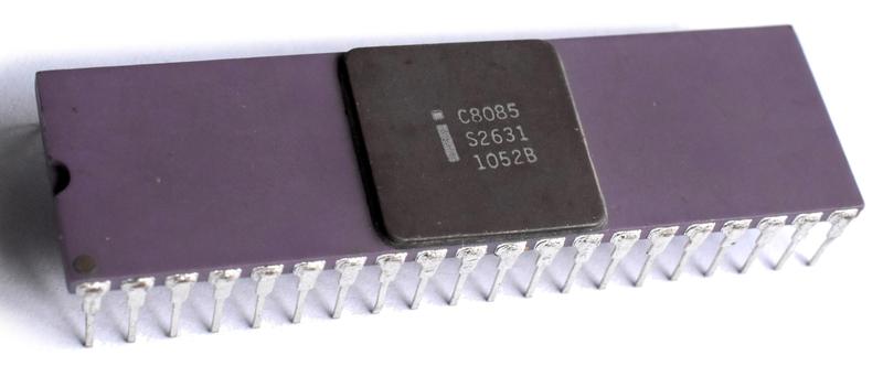
The Intel 8085, like the 8080 and the 8086, was packaged in a 40-pin DIP. Photo by Thomas Nguyen, (CC BY-SA 4.0).

The Intel 8085, like the 8080 and the 8086, was packaged in a 40-pin DIP. Photo by Thomas Nguyen, (CC BY-SA 4.0).

On the software side, the 8085 is curious: 12 instructions were added to the instruction set (finally using every opcode), but all but two were hidden and left undocumented.16 Moreover, the 8085 added two new condition codes, but these were also hidden. This situation occurred because the 8086 project started up in 1976, near the release of the 8085 chip. Intel wanted the 8086 to be compatible (to some extent) with the 8080 and 8085, but providing new instructions in the 8085 would make compatibility harder. It was too late to remove the instructions from the 8085 chip, so Intel did the next best thing and removed them from the documentation. These instructions are shown in red in the table below. Only the new SIM and RIM instructions were supported, necessary in order to use the 8085's new interrupt and serial I/O features.

 0123456701234567
0NOPLXI BSTAX BINX BINR BDCR BMVI BRLCMOV B,BMOV B,CMOV B,DMOV B,EMOV B,HMOV B,LMOV B,MMOV B,A
1DSUBDAD BLDAX BDCX BINR CDCR CMVI CRRCMOV C,BMOV C,CMOV C,DMOV C,EMOV C,HMOV C,LMOV C,MMOV C,A
2ARHLLXI DSTAX DINX DINR DDCR DMVI DRALMOV D,BMOV D,CMOV D,DMOV D,EMOV D,HMOV D,LMOV D,MMOV D,A
3RDELDAD DLDAX DDCX DINR EDCR EMVI ERARMOV E,BMOV E,CMOV E,DMOV E,EMOV E,HMOV E,LMOV E,MMOV E,A
4RIMLXI HSHLDINX HINR HDCR HMVI HDAAMOV H,BMOV H,CMOV H,DMOV H,EMOV H,HMOV H,LMOV H,MMOV H,A
5LDHIDAD HLHLDDCX HINR LDCR LMVI LCMAMOV L,BMOV L,CMOV L,DMOV L,EMOV L,HMOV L,LMOV L,MMOV L,A
6SIMLXI SPSTAINX SPINR MDCR MMVI MSTCMOV M,BMOV M,CMOV M,DMOV M,EMOV M,HMOV M,LHLTMOV M,A
7LDSIDAD SPLDADCX SPINR ADCR AMVI ACMCMOV A,BMOV A,CMOV A,DMOV A,EMOV A,HMOV A,LMOV A,MMOV A,A
0ADD BADD CADD DADD EADD HADD LADD MADD ARNZPOP BJNZJMPCNZPUSH BADIRST 0
1ADC BADC CADC DADC EADC HADC LADC MADC ARZRETJZRSTVCZCALLACIRST 1
2SUB BSUB CSUB DSUB ESUB HSUB LSUB MSUB ARNCPOP DJNCOUTCNCPUSH DSUIRST 2
3SBB BSBB CSBB DSBB ESBB HSBB LSBB MSBB ARCSHLXJCINCCJNKSBIRST 3
4ANA BANA CANA DANA EANA HANA LANA MANA ARPOPOP HJPOXTHLCPOPUSH HANIRST 4
5XRA BXRA CXRA DXRA EXRA HXRA LXRA MXRA ARPEPCHLJPEXCHGCPELHLXXRIRST 5
6ORA BORA CORA DORA EORA HORA LORA MORA ARPPOP PSWJPDICPPUSH PSWORIRST 6
7CMP BCMP CCMP DCMP ECMP HCMP LCMP MCMP ARMSPHLJMEICMJKCPIRST 7

Intel 8086

Following the 8080, Intel intended to revolutionize microprocessors with a 32-bit "micro-mainframe", the iAPX 432. This extremely complex processor implemented objects, memory management, interprocess communication, and fine-grained memory protection in hardware. The iAPX 432 was too ambitious and the project fell behind schedule, leaving Intel vulnerable against competitors such as Motorola and Zilog. Intel quickly threw together a 16-bit processor as a stopgap until the iAPX 432 was ready; to show its continuity with the 8-bit processor line, this processor was called the 8086. The iAPX 432 ended up being one of the great disaster stories of modern computing and quietly disappeared.

The "stopgap" 8086 processor, however, started the x86 architecture that changed the history of Intel. The 8086's victory was powered by the IBM PC, designed in 1981 around the Intel 8088, a variant of the 8086 with a cheaper 8-bit bus. The IBM PC was a rousing success, defining the modern computer and making Intel's fortune. Intel produced a succession of more powerful chips that extended the 8086: 286, 386, 486, Pentium, and so on, leading to the current x86 architecture.

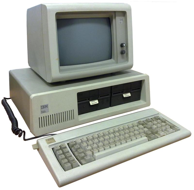
The original IBM PC used the Intel 8088 processor, a variant of the 8086 with an 8-bit bus. Photo by Ruben de Rijcke, (CC BY-SA 3.0).

The original IBM PC used the Intel 8088 processor, a variant of the 8086 with an 8-bit bus. Photo by Ruben de Rijcke, (CC BY-SA 3.0).

The 8086 was a major change from the 8080/8085, jumping from an 8-bit architecture to a 16-bit architecture and expanding from 64K of memory to 1 megabyte. Nonetheless, the 8086's architecture is closely related to the 8080. The designers of the 8086 wanted it to be compatible with the 8080/8085, but the difference was too wide for binary compatibility or even assembly-language compatibility. Instead, the 8086 was designed so a program could translate 8080 assembly language to 8086 assembly language.17 To accomplish this, each 8080 register had a corresponding 8086 register and most 8080 instructions had corresponding 8086 instructions.

The 8086's instruction set was designed with a new concept, the "ModR/M" byte, which usually follows the opcode byte. The ModR/M byte specifies the memory addressing mode and the register (or registers) to use, allowing that information to be moved out of the opcode. For instance, where the 8080 had a quadrant of 64 instructions to move from register to register, the 8086 has a single move instruction, with the ModR/M byte specifying the particular instruction. (The move instruction, however, has variants to handle byte vs. word operations, moves to or from memory, and so forth, so the 8086 ends up with a few move opcodes.) The ModR/M byte preserves the Datapoint 2200's concept of using the same instruction for memory and register operations, but allows a memory address to be provided in the instruction.

The 8086 also cleans up some of the historical baggage in the instruction set, freeing up space in the precious 256 opcodes for new instructions. The conditional call and return instructions were eliminated, while the conditional jumps were expanded. The 8008's RST (Restart) instructions were eliminated, replaced by interrupt vectors.

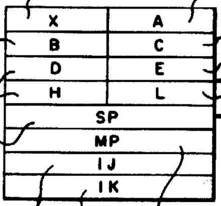
The 8086 extended its registers to 16 bits and added several new registers. An Intel patent (below) shows that the 8086's registers were originally called A, B, C, D, E, H, and L, matching the Datapoint 2200. The A register was extended to the 16-bit XA register, while the BC, DE, and HL registers were used unchanged. When the 8086 was released, these registers were renamed to AX, CX, DX, and BX respectively.18 In particular, the HL register was renamed to BX; this is why BX can specify a memory address in the ModR/M byte, but AX, CX, and DX can't.

A patent diagram showing the 8086's registers with their original names.  (MP, IJ, and IK are now known as BP, SI, and DI.) From patent US4449184.

A patent diagram showing the 8086's registers with their original names. (MP, IJ, and IK are now known as BP, SI, and DI.) From patent US4449184.

The table below shows the 8086's instruction set, with "b", "w", and "i" indicating byte (8-bit), word (16-bit), and immediate instructions. The Datapoint 2200 instructions (colored) are all still supported. The number of Datapoint instructions looks small because the ModR/M byte collapses groups of old opcodes into a single new one. This opened up space in the opcode table, though, allowing the 8086 to have many new instructions as well as 16-bit instructions.19

 0123456701234567
0ADD bADD wADD bADD wADD biADD wiPUSH ESPOP ESINC AXINC CXINC DXINC BXINC SPINC BPINC SIINC DI
1OR bOR wOR bOR wOR biOR wiPUSH CS DEC AXDEC CXDEC DXDEC BXDEC SPDEC BPDEC SIDEC DI
2ADC bADC wADC bADC wADC biADC wiPUSH SSPOP SSPUSH AXPUSH CXPUSH DXPUSH BXPUSH SPPUSH BPPUSH SIPUSH DI
3SBB bSBB wSBB bSBB wSBB biSBB wiPUSH DSPOP DSPOP AXPOP CXPOP DXPOP BXPOP SPPOP BPPOP SIPOP DI
4AND bAND wAND bAND wAND biAND wiES:DAA        
5SUB bSUB wSUB bSUB wSUB biSUB wiCS:DAS        
6XOR bXOR wXOR bXOR wXOR biXOR wiSS:AAAJOJNOJBJNBJZJNZJBEJA
7CMP bCMP wCMP bCMP wCMP biCMP wiDS:AASJSJNSJPEJPOJLJGEJLEJG
0GRP1 bGRP1 wGRP1 bGRP1 wTEST bTEST wXCHG bXCHG w  RETRETLESLDSMOV bMOV w
1MOV bMOV wMOV bMOV wMOV srLEAMOV srPOP  RETFRETFINT 3INTINTOIRET
2NOPXCHG CXXCHG DXXCHG BXXCHG SPXCHG BPXCHG SIXCHG DIShift bShift wShift bShift wAAMAAD XLAT
3CBWCWDCALLWAITPUSHFPOPFSAHFLAHFESC 0ESC 1ESC 2ESC 3ESC 4ESC 5ESC 6ESC 7
4MOV AL,MMOV AX,MMOV M,ALMOV M,AXMOVS bMOVS wCMPS bCMPS wLOOPNZLOOPZLOOPJCXZIN bIN wOUT bOUT w
5TEST bTEST wSTOS bSTOS wLODS bLODS wSCAS bSCAS wCALLJMPJMPJMPIN bIN wOUT b DXOUT w DX
6MOV AL,iMOV CL,iMOV DL,iMOV BL,iMOV AH,iMOV CH,iMOV DH,iMOV BH,iLOCK REPNZREPZHLTCMCGRP3aGRP3b
7MOV AX,iMOV CX,iMOV DX,iMOV BX,iMOV SP,iMOV BP,iMOV SI,iMOV DI,iCLCSTCCLISTICLDSTDGRP4GRP5

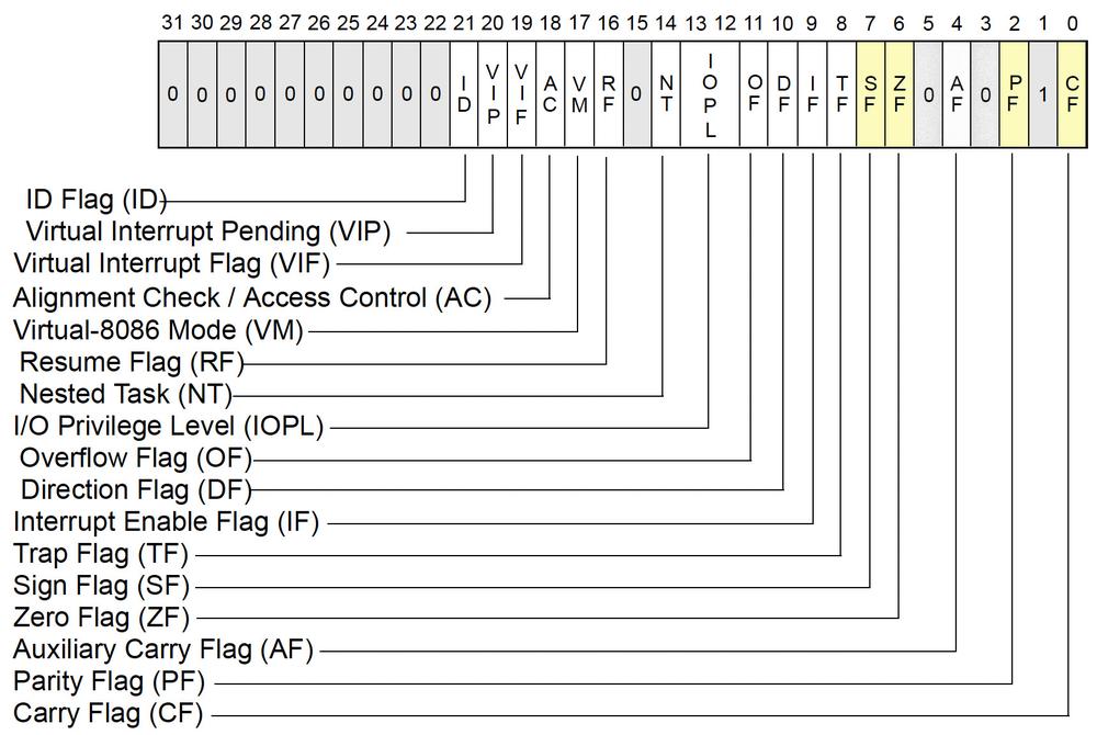
The 8086 has a 16-bit flags register, shown below, but the low byte remained compatible with the 8080. The four highlighted flags (sign, zero, parity, and carry) are the ones originating in the Datapoint 2200.

The flag word of the 8086 contains the original Datapoint 2200 registers.

The flag word of the 8086 contains the original Datapoint 2200 registers.

Modern x86 and x86-64

The modern x86 architecture has extended the 8086 to a 32-bit architecture (IA-32) and a 64-bit architecture (x86-6420), but the Datapoint features remain. At startup, an x86 processor runs in "real mode", which operates like the original 8086. More interesting is 64-bit mode, which has some major architectural changes. In 64-bit mode, the 8086's general-purpose registers are extended to sixteen 64-bit registers (and soon to be 32 registers). However, the original Datapoint registers are special and can still be accessed as byte registers within the corresponding 64-bit register; these are highlighted in the table below.21

General purpose registers in x86-64. From Intel Software Developer's Manual.

General purpose registers in x86-64. From Intel Software Developer's Manual.

The flag register of the 8086 was extended to 32 bits or 64 bits in x86. As the diagram below shows, the original Datapoint 2200 status flags are still there (highlighted in yellow).

The 32-bit and 64-bit flags of x86 contain the original Datapoint 2200 registers. From Intel Software Developer's Manual.

The 32-bit and 64-bit flags of x86 contain the original Datapoint 2200 registers. From Intel Software Developer's Manual.

The instruction set in x86 has been extended from the 8086, mostly through prefixes, but the instructions from the Datapoint 2200 are still there. The ModR/M byte was changed in 32-bit mode so the BX (originally HL) register is no longer special when accessing memory (although it's still special with 16-bit addressing, until Intel removes that in the upcoming x86-S simplification.) I/O ports still exist in x86, although they are viewed as more of a legacy feature: modern I/O devices typically use memory-mapped I/O instead of I/O ports. To summarize, fifty years later, x86-64 is slowly moving away from some of the Datapoint 2200 features, but they are still there.

Conclusions

The modern x86 architecture is descended from the Datapoint 2200's architecture. Because there is backward-compatibility at each step, you should theoretically be able to take a Datapoint 2200 binary, disassemble it to 8008 assembly, automatically translate it to 8080 assembly, automatically convert it to 8086 assembly, and then run it on a modern x86 processor. (The I/O devices would be different and cause trouble, of course.)

The Datapoint 2200's complete instruction set, its flags, and its little-endian architecture have persisted into current processors. This shows the critical importance of backward compatibility to customers. While Intel keeps attempting to create new architectures (iAPX 432, i960, i860, Itanium), customers would rather stay on a compatible architecture. Remarkably, Intel has managed to move from 8-bit computers to 16, 32, and 64 bits, while keeping systems mostly compatible. As a result, design decisions made for the Datapoint 2200 over 50 years ago are still impacting modern computers. Will processors still have the features of the Datapoint 2200 another fifty years from now? I wouldn't be surprised.22

Thanks to Joe Oberhauser for suggesting this topic. I plan to write more on the 8086, so follow me on Twitter @kenshirriff or RSS for updates. I've also started experimenting with Mastodon recently as @[email protected] so you can follow me there too.

Notes and references

  1. Shift-register memory was also used in the TV Typewriter (1973) and the display storage of the Apple I (1976). However, dynamic RAM (DRAM) rapidly dropped in price, making shift-register memory obsolete by the mid 1970s. (I wrote about the Intel 1405 shift register memory in detail in this article.) 

  2. For comparison, the popular PDP-8 minicomputer had just two main registers: the accumulator and a multiplier-quotient register; instructions typically operated on the accumulator and a memory location. The Data General Nova, a minicomputer released in 1969, had four accumulator / index registers. Mainframes generally had many more registers; the IBM System/360 (1964), for instance, had 16 general registers and four floating-point registers. 

  3. On the hardware side, instructions were decoded with BCD-to-decimal decoder chips (type 7442). These decoders normally decoded a 4-bit BCD value into one of 10 output lines. In the Datapoint 2200, they decoded a 3-bit value into one of 8 output lines, and the other two lines were ignored. This allowed the high-bit line to be used as a selection line; if it was set, none of the 8 outputs would be active. 

  4. These bit patterns map cleanly onto octal, so the opcodes are clearest when specified in octal. This octal structure has persisted in Intel processors including modern x86 processors. Unfortunately, Intel invariably specifies the opcodes in hexadecimal rather than octal, which obscures the underlying structure. This structure is described in detail in The 80x86 is an Octal Machine

  5. It is unusual for an instruction set to require memory addresses to be loaded into a register in order to access memory. This technique was common in microcode, where memory addresses were loaded into the Memory Address Register (MAR). As pwg pointed out, the CDC mainframes (e.g. 6600) had special address registers; when you changed an address register, the specified memory location was read or written to the corresponding operand register automatically.

    At first, I thought that serial memory might motivate the use of an address register, but I don't think there's a connection. Most likely, the Datapoint 2200 used these techniques to create a simple, orthogonal instruction set that was easy to decode, and they weren't particularly concerned with performance. 

  6. The instruction tables in this article are different from most articles, because I use octal instead of hexadecimal. (Displaying an octal-based instruction in a hexadecimal table obscures much of the underlying structure.) To display the table in octal, I break it into four quadrants based on the top octal digit of a three-digit opcode: 0, 1, 2, or 3. The digit 0-7 along the left is the middle octal digit and the digit along the top is the low octal digit. 

  7. The regular pattern of Load instructions is broken by the NOP and HALT instructions. All the register-to-register load instructions along the diagonal accomplish nothing since they move a register to itself, but only the first one is explicitly called NOP. Moving a memory location to itself doesn't make sense, so its opcode is assigned the HALT instruction. Note that the all-0's opcode and the all-1's opcode are both HALT instructions. This is useful since it can stop execution if the program tries executing uninitialized memory. 

  8. You might think that Datapoint and Intel used the same ALU operations simply because they are the obvious set of 8 operations. However, if you look at other processors around that time, they use a wide variety of ALU operations. Similarly, the status flags in the Datapoint 2200 aren't the obvious set; systems with four flags typically used Sign, Carry, Zero, and Overflow (not Parity). Parity is surprisingly expensive to implement on a standard processor, but (as Philip Freidin pointed out) parity is cheap on a serial processor like the Datapoint 2200. Intel processors didn't provide an Overflow flag until the 8086; even the 8080 didn't have it although the Motorola 6800 and MOS 6502 did. The 8085 implemented an overflow flag (V) but it was left undocumented. 

  9. You might wonder if the Datapoint 2200 (and 8008) could be considered RISC processors since they have simple, easy-to-decode instruction sets. I think it is a mistake to try to wedge every processor into the RISC or CISC categories (Reduced Instruction Set Computer or Complex Instruction Set Computer). In particular, the Datapoint 2200 wasn't designed with the RISC philosophy (make a processor more powerful by simplifying the instruction set), its instruction set architecture is very different from RISC chips, and its implementation is different from RISC chips. Similarly, it wasn't designed with a CISC philosophy (make a processor more powerful by narrowing the semantic gap with high-level languages) and it doesn't look like a CISC chip.

    So where does that leave the Datapoint 2200? In "RISC: Back to the future?", famed computer architect Gordon Bell uses the term MISC (Minimal Instruction Set Computer) to describe the architecture of simple, early computers and microprocessors such as the Manchester Mark I (1948), the PDP-8 minicomputer (1966), and the Intel 4004 (1971). Computer architecture evolved from these early hardwired "simple computers" to microprogrammed processors, processors with cache, and hardwired, pipelined processors. "Minimal Instruction Set Computer" seems like a good description of the Datapoint 2200, since it is about the smallest, simplest processor that could get the job done. 

  10. Many people think that the Intel 8008 is an extension of the 4-bit Intel 4004 processor, but they are completely unrelated aside from the part numbers. The Intel 4004 is a 4-bit processor designed to implement a calculator for a company called Busicom. Its architecture is completely different from the 8008. In particular, the 4004 is a "Harvard architecture" system, with data storage and instruction storage completely separate. The 4004 also has a fairly strange instruction set, designed for calculators. For instance, it has a special instruction to convert a keyboard scan code to binary. The 4004 team and the 8008 team at Intel had many people in common, however, so the two chips have physical layouts (floorplans) that are very similar. 

  11. In this article, I'm focusing on the Datapoint 2200 Version I. Any time I refer to the Datapoint 2200, I mean the version I specifically. The Version II has an expanded instruction set, but it was expanded in an entirely different direction from the Intel 8080, so it's not relevant to this post. The Version II is interesting, however, since it provides a perspective of how the Intel 8080 could have developed in an "alternate universe". 

  12. Federico Faggin wrote The Birth of the Microprocessor in Byte Magazine, March 1992. This article describes in some detail the creation of the 8008 and 8080.

    The Oral History of the 8080 discusses many of the problems with the 8008 and how the 8080 addressed them. (See page 4.) Masatoshi Shima, one of the architects of the 4004, described five problems with the 8008: It was slow because it used two clock cycles per state. It had no general-purpose stack and was weak with interrupts. It had limited memory and I/O space. The instruction set was primitive, with only 8-bit data, limited addressing, and a single address pointer register. Finally, the system bus required a lot of interface circuitry. (See page 7.) 

  13. The 8080 is often said to be the "first truly usable microprocessor". Supposedly the source of this quote is Forgotten PC history, but the statement doesn't appear there. I haven't been able to find the original source of this statement, so let me know. In any case, I don't think that statement is particularly accurate, as the Motorola 6800 was "truly usable" and came out before the Intel 8080.

    The 8080 was first in one important way, though: it was Intel's first microprocessor that was designed with feedback from customers. Both the 4004 and the 8008 were custom chips for a single company. The 8080, however, was based on extensive customer feedback about the flaws in the 8008 and what features customers wanted. The 8080 oral history discusses this in more detail. 

  14. The 8008 was built with PMOS circuitry, while the 8080 was built with NMOS. This may seem like a trivial difference, but NMOS provided much superior performance. NMOS became the standard microprocessor technology until the rise of CMOS in the 1980s, combining NMOS and PMOS to dramatically reduce power consumption.

    Another key hardware improvement was that the 8080 used a 40-pin package, compared to the 18-pin package of the 8008. Intel had long followed the "religion" of small 16-pin packages, and only reluctantly moved to 18 pins (as in the 8008). However, by the time the 8080 was introduced, Intel recognized the utility of industry-standard 40-pin packages. The additional pins made the 8080 much easier to interface to a system. Moreover, the 8080's 16-bit address bus supported four times the memory of the 8008's 14-bit address bus. (The 40-pin package was still small for the time; some companies used 50-pin or 64-pin packages for microprocessors.) 

  15. The 8080 is not binary-compatible with the 8008 because almost all the instructions were shifted to different opcodes. One important but subtle change was that the 8 register/memory codes were reordered to start with B instead of A. The motivation is that this gave registers in a 16-bit register pair (BC, DE, or HL) codes that differ only in the low bit. This makes it easier to specify a register pair with a two-bit code. 

  16. Stan Mazor (one of the creators of the 4004 and 8080) explained that the 8085 removed 10 of the 12 new instructions because "they would burden the 8086 instruction set." Because the decision came near the 8085's release, they would "leave all 12 instructions on the already designed 8085 CPU chip, but document and announce only two of them" since modifying a CPU is hard but modifying a CPU's paper reference manual is easy.

    Several of the Intel 8086 engineers provided a similar explanation in Intel Microprocessors: 8008 to 8086: While the 8085 provided the new RIM and SIM instructions, "several other instructions that had been contemplated were not made available because of the software ramifications and the compatibility constraints they would place on the forthcoming 8086."

    For more information on the 8085's undocumented instructions, see Unspecified 8085 op codes enhance programming. The two new condition flags were V (2's complement overflow) and X5 (underflow on decrement or overflow on increment). The opcodes were DSUB (double (i.e. 16-bit) subtraction), ARHL (arithmetic shift right of HL), RDEL (rotate DE left through carry), LDHI (load DE with HL plus an immediate byte), LDSI (load DE with SP plus an immediate byte), RSTV (restart on overflow), LHLX (load HL indirect through DE), SHLX (store HL indirect through DE), JX5 (jump on X5), and JNX5 (jump on not X5). 

  17. Conversion from 8080 assembly code to 8086 assembly code was performed with a tool called CONV86. Each line of 8080 assembly code was converted to the corresponding line (or sometimes a few lines) of 8086 assembly code. The program wasn't perfect, so it was expected that the user would need to do some manual editing. In particular, CONV86 couldn't handle self-modifying code, where the program changed its own instructions. (Nowadays, self-modifying code is almost never used, but it was more common in the 1970s in order to make code smaller and get more performance.) CONV86 also didn't handle the 8085's RIM and SIM instructions, recommending a rewrite if code used these instructions heavily.

    Writing programs in 8086 assembly code manually was better, of course, since the program could take advantage of the 8086's new features. Moreover, a program converted by CONV86 might be 25% larger, due to the 8086's use of two-byte instructions and inefficiencies in the conversion. 

  18. This renaming is why the instruction set has the registers in the order AX, CX, DX, BX, rather than in alphabetical order as you might expect. The other factor is that Intel decided that AX, BX, CX, and DX corresponded to Accumulator, Base, Count, and Data, so they couldn't assign the names arbitrarily. 

  19. A few notes on how the 8086's instructions relate to the earlier machines, since the ModR/M byte and 8- vs. 16-bit instructions make things a bit confusing. For an instruction like ADD, I have three 8-bit opcodes highlighted: an add to memory/register, an add from memory/register, and an immediate add. The neighboring unhighlighted opcodes are the corresponding 16-bit versions. Likewise, for MOV, I have highlighted the 8-bit moves to/from a register/memory. 

  20. Since the x86's 32-bit architecture is called IA-32, you might expect that IA-64 would be the 64-bit architecture. Instead, IA-64 is the completely different architecture used in the ill-fated Itanium. IA-64 was supposed to replace IA-32, despite being completely incompatible. Since AMD was cut out of IA-64, AMD developed their own 64-bit extension of the existing x86 architecture and called it AMD64. Customers flocked to this architecture while the Itanium languished. Intel reluctantly copied the AMD64 architecture, calling it Intel 64. 

  21. The x86 architecture allows byte access to certain parts of the larger registers (accessing AL, AH, etc.) as well as word and larger accesses. These partial-width reads and writes to registers make the implementation of the processor harder due to register renaming. The problem is that writing to part of a register means that the register's value is a combination of the old and new values. The Register Alias Table in the P6 architecture deals with this by adding a size field to each entry. If you write a short value and then read a longer value, the pipeline stalls to figure out the right value. Moreover, some 16-bit code uses the two 8-bit parts of a register as independent registers. To support this, the Register Alias Table keeps separate entries for the high and low byte. (For details, see the book Modern Processor Design, in particular the chapter on Intel's P6 Microarchitecture.) The point of this is that obscure features of the Datapoint 2200 (such as H and L acting as a combined register) can cause implementation difficulties 50 years later. 

  22. Some miscellaneous references: For a detailed history of the Datapoint 2200, see Datapoint: The Lost Story of the Texans Who Invented the Personal Computer Revolution. The 8008 oral history provides a lot of interesting information on the development of the 8008. For another look at the Datapoint 2200 and instruction sets, see Comparing Datapoint 2200, 8008, 8080 and Z80 Instruction Sets