Showing posts sorted by date for query 8086. Sort by relevance Show all posts

Reverse engineering the 59-pound printer onboard the Space Shuttle

The Space Shuttle contained a bulky printer so the astronauts could receive procedures, mission plans, weather reports, crew activity plans, and other documents. Needed for the first Shuttle launch in 1981, this printer was designed in just 7 months, built around an Army communications terminal. Unlike modern printers, the Shuttle's printer contains a spinning metal drum with raised characters, allowing it to rapidly print a line at a time.

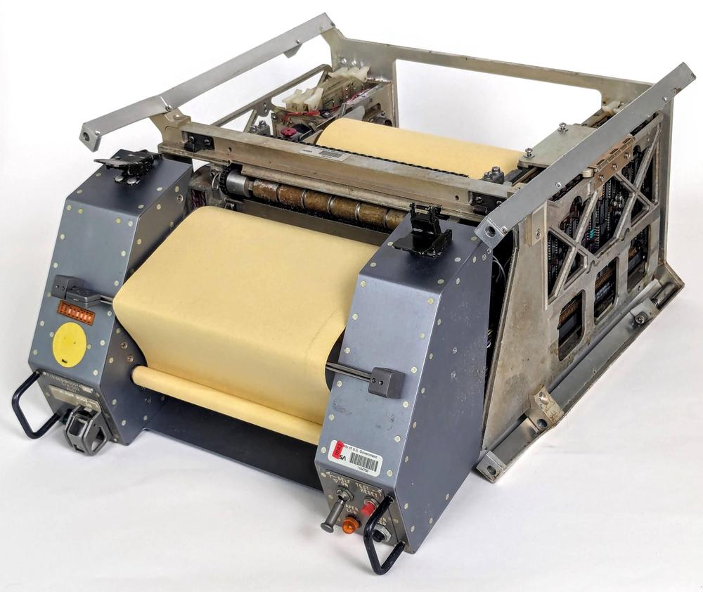
The Space Shuttle's Interim Teleprinter. The horizontal rails allowed it to be mounted in a Space Shuttle stowage locker.

The Space Shuttle's Interim Teleprinter. The horizontal rails allowed it to be mounted in a Space Shuttle stowage locker. Click this image (or any other) for a larger version.

This printer is known as the Space Shuttle Interim Teleprinter System.1 As the name "Interim" suggests, this printer was intended as a stop-gap measure, operating for a few flights until a better printer was operational. However, the teleprinter proved to be more reliable than its replacement, so it remained in use as a backup for over 50 flights, often printing thousands of lines per flight. This didn't come cheap: with a Shuttle flight costing $27,000 per pound, putting the 59-pound teleprinter in space cost over $1.5 million per flight.

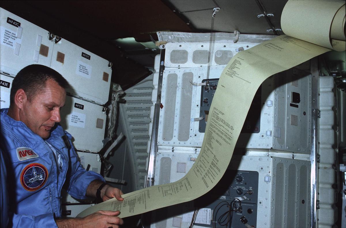
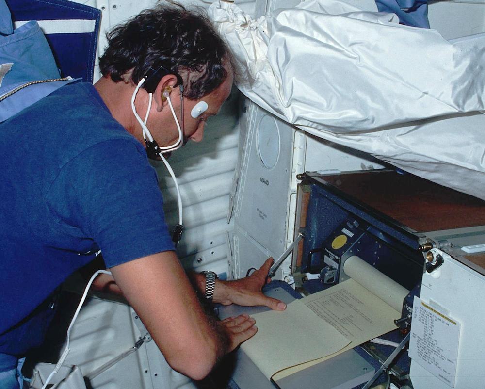
Pilot Overmyer reading a printout from the teleprinter, STS-5, November 16, 1982. From National Archives. The description says that this output is from the Text and Graphics System, but the yellow paper and the date show that this is the Interim Teleprinter.

Pilot Overmyer reading a printout from the teleprinter, STS-5, November 16, 1982. From National Archives. The description says that this output is from the Text and Graphics System, but the yellow paper and the date show that this is the Interim Teleprinter.

We obtained access to a Shuttle teleprinter (probably a development system that remained on the ground) and wanted to put it into operation. I had to reverse engineer three of the boards inside the printer to determine the data format the printer accepted: serial data encoded into audio. But after analyzing the printer and performing a lot of maintenance, we succeeded in getting the printer to print. In this article, I'll describe the Shuttle's Interim Teleprinter, explain its circuitry and drum-based printing mechanism, and show it in operation.

History of the Shuttle's Interim Teleprinter

The motivation for the teleprinter goes back to the Apollo program. During Apollo missions, the only way to send information to the astronauts was by talking to them over the radio and having the astronauts write down the data. NASA decided that the Space Shuttle should include a mechanism to send text and images to the astronauts, a 78-pound, high-tech fax machine called the Uplink Text & Graphics System (TAGS). A high-resolution grayscale image was sent to the Shuttle as a digital data stream. Onboard the Shuttle, a squat CRT displayed the image one line at a time and a fiber-optic faceplate transferred each line to light-sensitive silver emulsion paper. The paper was developed by passing it over a hot roller at 260ºF for 25 seconds, creating a permanent image.

The one flaw in this plan was that sending the digital image to the Shuttle required the Tracking and Data Relay Satellite System (TDRS), which due to delays wouldn't be ready until the sixth Shuttle flight. (The TDRS was a space-based replacement for the worldwide network of ground stations that was used during Apollo.) As a result, NASA decided just seven months before the first Shuttle launch that they needed an interim system "for transmission of real-time, flight-plan changes and other operational data to the crew."2

The Shuttle teleprinter is the result of this rushed effort to create a printer that could work over the existing audio channel rather than the digital TDRS satellite. Due to the time pressure, the Shuttle teleprinter needed to be based on an off-the-shelf printer. Thermal and electrostatic printers were rejected due to toxicity and flammability problems. (The Shuttle teleprinter used a roll of yellowish paper, which required a NASA waiver due to its flammability, a concern ever since the Apollo-1 disaster).

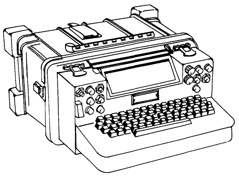
The AN/UGC-74 military communications terminal. This terminal was developed by the Army but also used by the Navy and Air Force. Image from the Operator's Manual, TM 11-5815-602-10.

The AN/UGC-74 military communications terminal. This terminal was developed by the Army but also used by the Navy and Air Force. Image from the Operator's Manual, TM 11-5815-602-10.

The decision was made to use a military communications terminal, the the AN/UGC-743 "Tactical Teletype". The terminal's interfacing was very flexible, supporting serial data in either ASCII or Baudot format, with multiple configurations and baud rates (up to 1200 baud), using either a current-loop or voltage signals. The military terminal supported two-way communication, so it had a keyboard. Remarkably, the terminal also implemented a word processor, controlled by a Motorola 6800 microprocessor (ancestor of the famous MOS 6502). The word processor allowed messages to be composed offline, minimizing the radio transmission time, which was important in a hostile environment. As will be seen, this 100-pound military system required many large changes to be usable on the Space Shuttle, most visibly removing the keyboard.

The printing mechanism

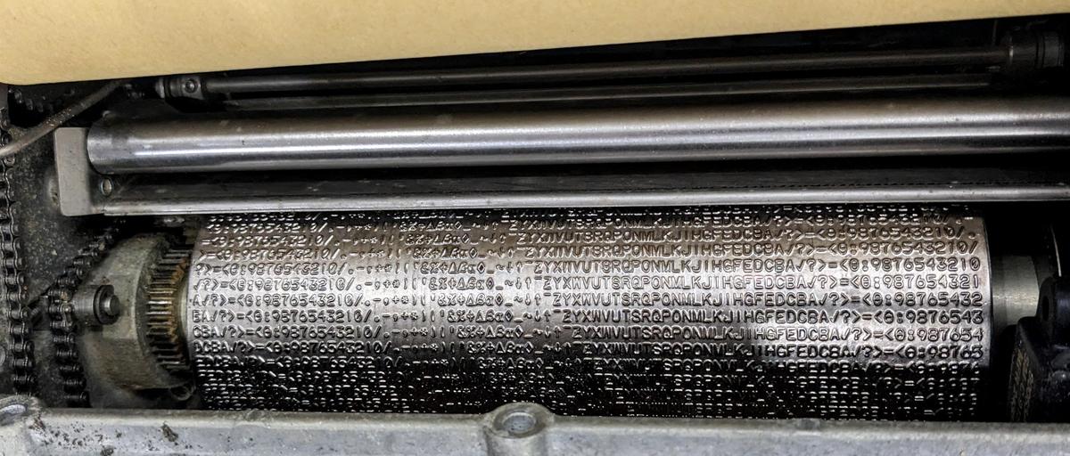
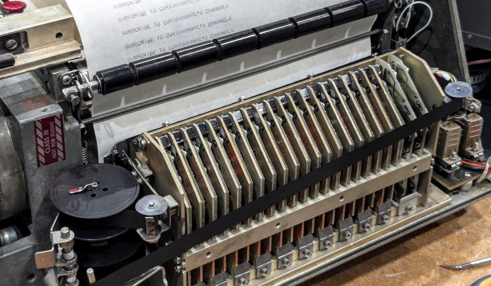
The teleprinter uses a spinning drum with raised characters, shown below.4 To print a character, the printer fires a hammer, forcing the inked ribbon and paper against the raised character on the drum. The drum is 80 characters wide, matching the line length, and there are 80 corresponding hammers, one for each print position. The drum has 64 printable characters, wrapped around each position of the drum.

The printer's drum rotating drum has 64 raised characters in each column. The characters spiral around the drum and are in reverse order, minimizing the chance that a line will fire all the hammers near-simultaneously.

The printer's drum rotating drum has 64 raised characters in each column. The characters spiral around the drum and are in reverse order, minimizing the chance that a line will fire all the hammers near-simultaneously.

The printer prints a line at a time, not instantaneously, but during each revolution of the drum. When the drum makes one complete revolution, each of the 64 characters passes by each print position once. Printing requires precise timing of the hammers to strike the right character on the drum as it whizzes by. The printer control circuitry triggers each hammer at the proper time, when the desired character on the drum is lined up with the hammer, producing the desired text.5

The character set is slightly different between the military printer and the Shuttle printer. The military drum had 64 ASCII characters (upper-case letters only, numbers, and special characters). The drum doesn't contain an explicit space character, since nothing is printed for a space. In its place, the drum has a diamond "◊", used as a special character to indicate a parity error or other error. The drum for the Shuttle teleprinter replaces 10 ASCII special characters with symbols that are more useful to the Shuttle, such as Greek letters for angles. Specifically, the characters ;@[\]^!"#$ are replaced by θ✓‾↑↓~αβΔϕ.

With the teleprinter disassembled, the 20 hammer cards are visible at the front. Two hammer driver cards are to the right of the hammer cards.

With the teleprinter disassembled, the 20 hammer cards are visible at the front. Two hammer driver cards are to the right of the hammer cards.

The video below shows a closeup of the hammers as they strike the paper to print text. The text is the teleprinter's built-in test message: "THE LAZY YELLOW DOG WAS CAUGHT BY THE SLOW RED FOX AS HE LAY SLEEPING IN THE SUN". This test message is based on the traditional quick brown fox..., which is a pangram, containing all 26 letters, but the teleprinter's test sentence is missing J, K, M, Q, and V. However, the test message is exactly 80 characters long and replaces spaces with the diamond "◊", so it is effective for verifying that all 80 columns work.

The electronics

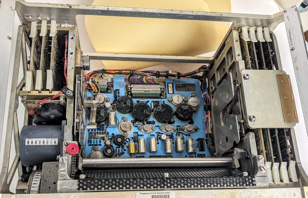
The photo below shows the circuitry inside the teleprinter, looking down from above. At the left are the three interface boards, custom boards that demodulate the incoming audio signal. In front of the interface boards are large inductors to filter the incoming power. Hidden beneath them, a solid-state relay controls the power to the rest of the printer, implementing the low-power standby mode. In the middle, the blue board is the surprisingly complex switching power supply, mounted on a thick metal plate for cooling. Normally, the large roll of paper is mounted above the power supply board. At the right, four large circuit boards implement the main logic of the printer: a printer driver board, a communications board, a memory board, and the processor board. The rotating drum is protected by the perforated black metal grill at the front.

Inside the Shuttle teleprinter, showing the electronics.

Inside the Shuttle teleprinter, showing the electronics.

The demodulator boards

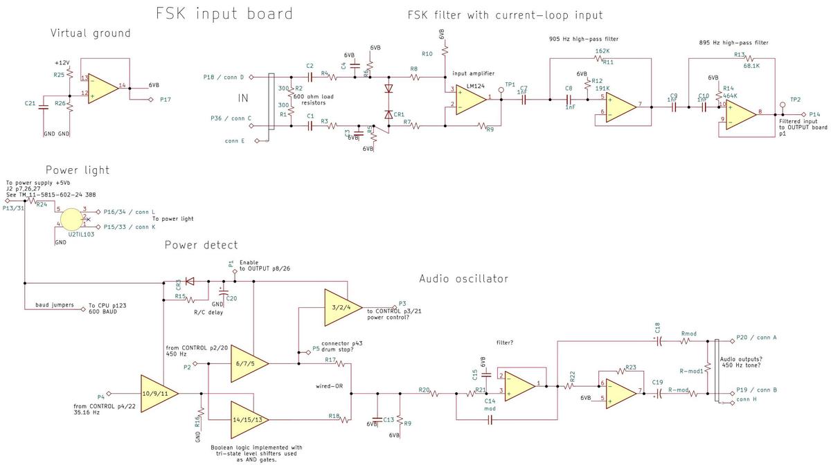
The original military teleprinter received data as a serial bitstream. However, on the Space Shuttle, data was encoded as frequencies on the audio link. Three custom boards were constructed to demodulate the audio data so the rest of the printer could handle it. These boards also performed Shuttle-specific tasks such as powering up the printer when a message comes in, and then returning the printer to standby mode. I reverse-engineered these boards to determine how they work and to determine the data encoding. (Schematics are in the footnotes.7) In this section, I'll discuss these three boards, which are on the left side of the printer.

To summarize, the serial bitstream is encoded with Frequency Shift Keying, with a 1 represented by 3600 Hz and a 0 represented by 7200 Hz.6 The serial data is transmitted at 600 baud, even parity, one stop bit. The demodulation process first converts the input audio to a digital signal by thresholding it. (That is, the input sine wave is converted to a square wave.) The digital signal is autocorrelated to distinguish the 3600 Hz and 7200 Hz signals, recovering the underlying serial data. This signal is passed to the printer's logic boards (part of the original military teleprinter), which convert the serial signal to ASCII bytes and prints them.

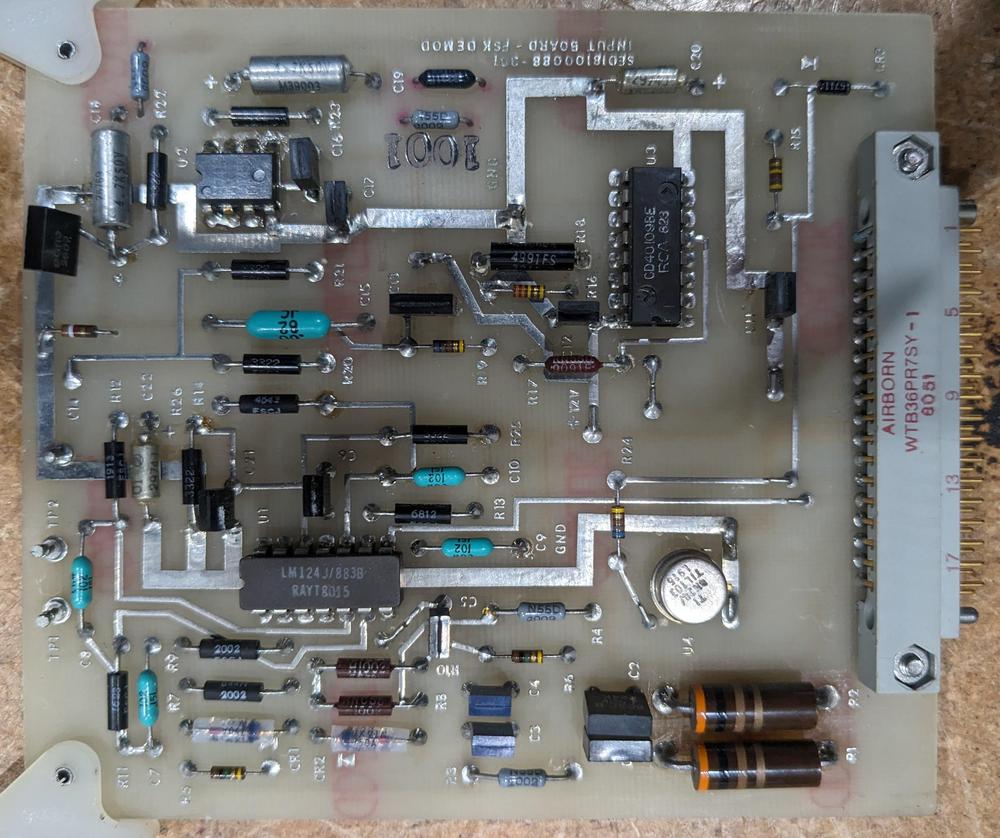
Signal processing starts with the "FSK input" board, shown below. First, it amplifies the input audio signal. (The two large resistors provide a 600 Ω load for the audio input.) Next, a 900 Hz high-pass filter eliminates low-frequency noise. (The filter is implemented by a two-stage Sallen-Key topology.)

The input board.

The input board.

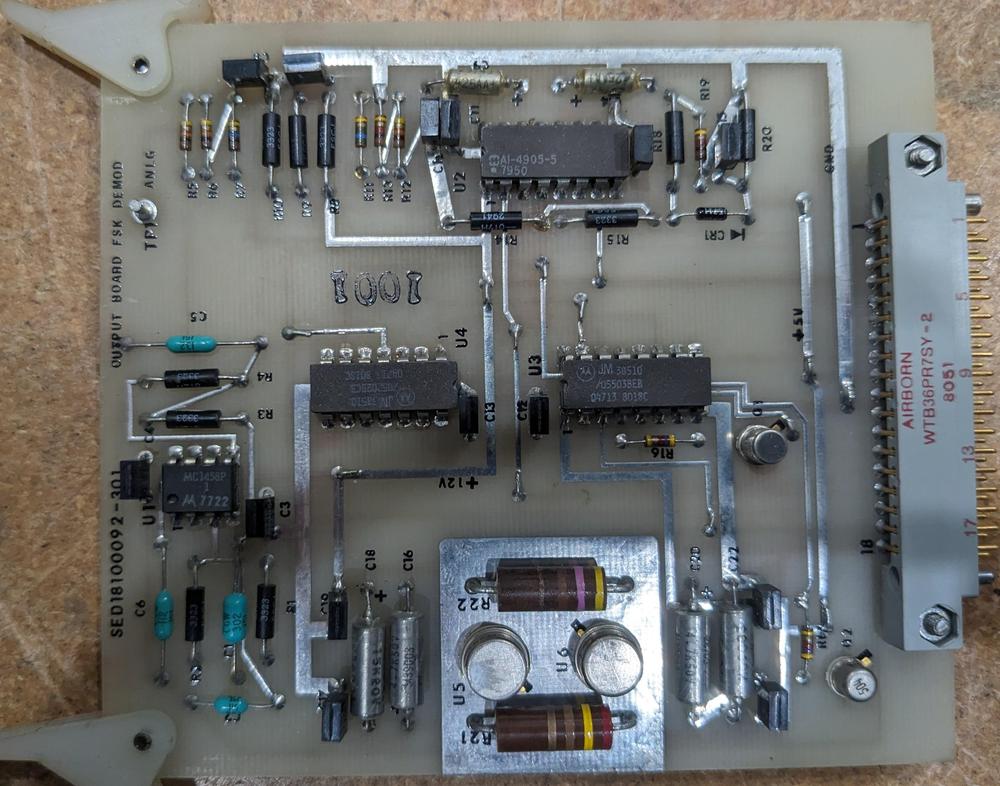
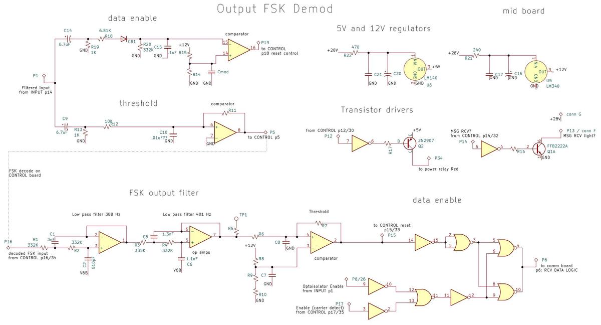
The signal bounces from board to board, going to the "output FSK demod" board next. This board has a carrier-detect circuit that turns on the rest of the printer if it detects an input signal. This allows the printer to sit idle until it receives a signal from Earth. This board also applies the threshold to the signal to turn it into a digital waveform, which goes to the "control" board.

The output board.

The output board.

The output board also holds the 5-volt and 12-volt linear regulators that power the three boards; these are the metal-can ICs at the bottom of the board. To reduce the load on the regulators, two large resistors drop the input voltage (28 volts) to a lower level before it is regulated.

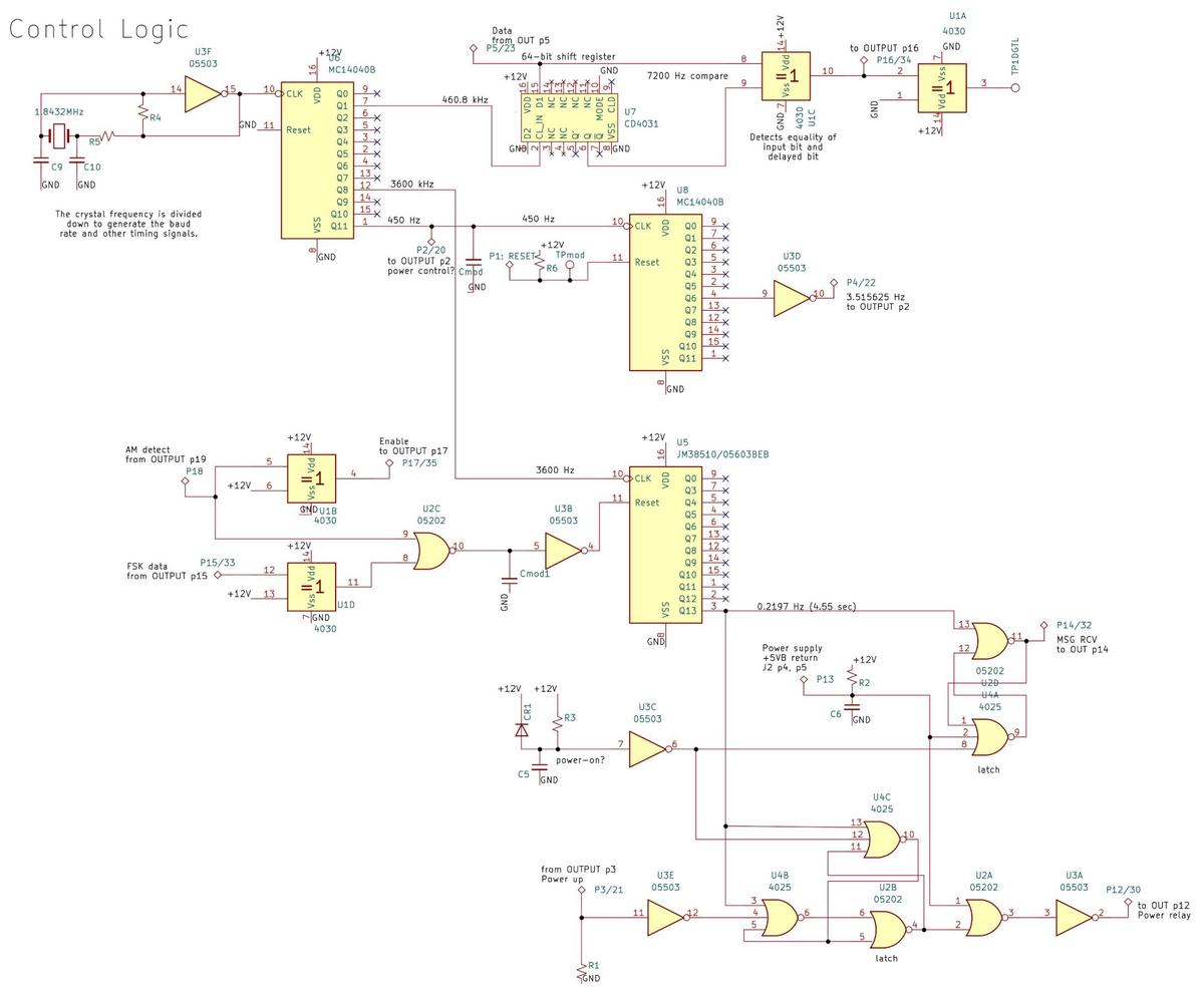
The control board holds the FSK decoder, an interesting circuit that converts the two FSK frequencies to binary by implementing a digital auto-correlator. It uses a 64-bit shift register to delay the digital input by 139 µs. The input and the delayed input are XOR'd together, generating a result that depends on the frequency. A 7200 Hz signal repeats every 139 µs, so the input and the delayed input match, yielding 0 from the XOR. However, a 3600 Hz square wave switches state every 139 µs, so the two XOR inputs will always differ, resulting in a 1 output. Thus, the circuit cleanly distinguishes between a 3600 Hz input and a 7200 Hz input.

The control board.

The control board.

The digital demodulator avoids some of the problems of an analog FSK demodulator. It is not sensitive to signal levels, since the signal is converted to digital. The digital demodulator is also not sensitive to harmonics, which can cause problems with analog demodulators. Finally, it doesn't require the carefully-tuned filters of an analog circuit.

The demodulated signal passes from the control board back to the output board. This board applies a 400 Hz low-pass filter and then a threshold to convert the signal back to binary. If the input frequencies are not exact, the demodulator will produce the correct 0 or 1 value over most of the waveform, but there will be glitches at the edges. The low-pass filter removes these glitches. (You might be concerned that a 600-baud signal would be wiped out by a 400 Hz low-pass filter. However, the worst case signal (alternating 0's and 1's) would be 300 Hz because it takes two bits to make one cycle, so the filter has plenty of margin.) Next, the board blocks the signal unless a carrier is detected. This ensures that random noise isn't demodulated and printed. Finally, the serial binary signal leaves the custom Shuttle boards and goes to the teleprinter's communication board, part of the standard teleprinter.

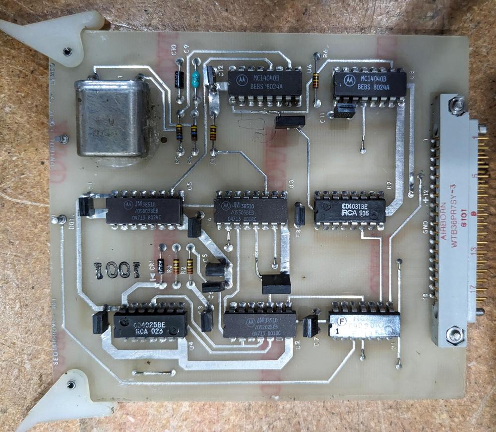
I noticed two unusual things about these boards. First, they have some modifications: "bodge" wires and added components. Second, the boards are not conformal coated, which is unusual for aerospace boards. (The four logic cards, in comparison, are protected with conformal coating.) My hypothesis is that these boards were development boards, early in the design process of the Shuttle teleprinter, so they were modified as the design changed. The teleprinter is also marked "Not for flight", which supports this theory.

Mission Specialist Thagard getting output from the teleprinter. Flight STS-7, June 24, 1983. From NARA. Although the description says this is the Text & Graphics System, it is clearly the Interim Teleprinter.

Mission Specialist Thagard getting output from the teleprinter. Flight STS-7, June 24, 1983. From NARA. Although the description says this is the Text & Graphics System, it is clearly the Interim Teleprinter.

The logic cards

The military teleprinter contained four logic circuit cards: a CPU card, a memory card, a communications card, and a print control card, mounted at the right rear of the teleprinter. These cards are used unchanged in the Shuttle teleprinter.

The circuitry is more complex than you might expect, with four large cards full of ICs. There are several reasons for this. First, the cards use 1970s microprocessor technology, so it takes a lot of circuitry to do anything. In particular, many simple 7400-series logic chips perform "glue" functions: decoding addresses, buffering data, latching signals, and so forth. Moreover, a drum printer is inherently complicated, since 80 hammers must be driven at the right time based on the desired characters. Third, the teleprinter is very flexible, supporting multiple signal levels and two character formats (ASCII and Baudot). Most surprisingly, the teleprinter implements a word processor, allowing messages to be composed and edited offline. Of course, since the Shuttle's teleprinter is only used to receive data, and doesn't even have a keyboard, the word processor feature is entirely useless.

The CPU card

The CPU card holds the microprocessor that controls the teleprinter. Its most important function is to convert a line of ASCII characters into print drum codes. These codes are stored in memory for use by the print control card. The CPU also implements configuration and self-test functions.

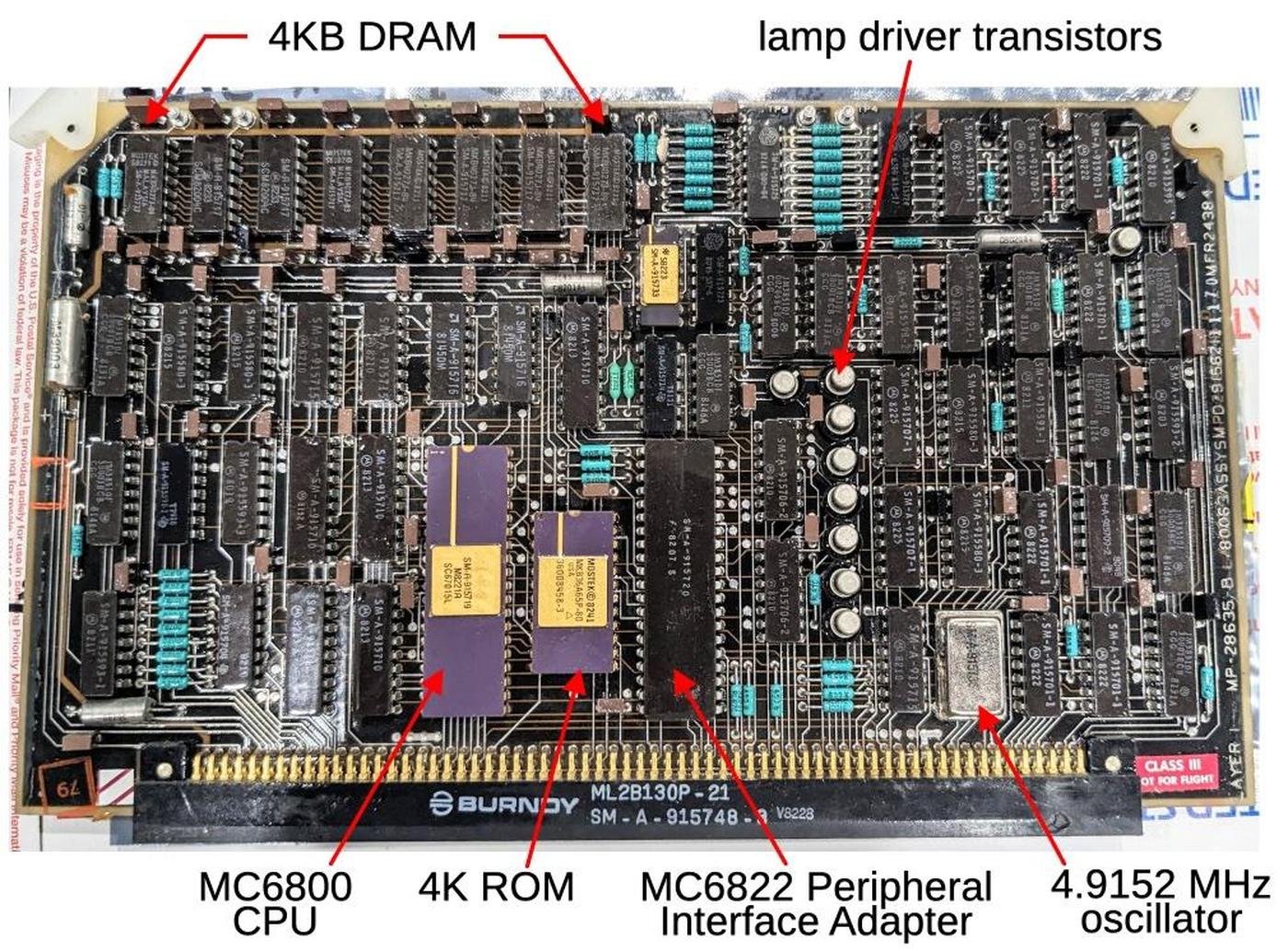
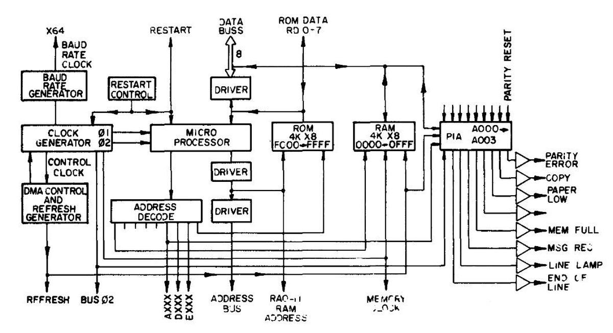
The diagram below shows some of the main components. The CPU card contains a Motorola 6800 CPU, 4 kilobytes of memory, and a ROM that holds its program code.8 Inconveniently, all the IC part numbers are military numbers so it takes some investigation to determine what a part really is. The MC6822 is a Peripheral Interface Adapter, a Motorola chip that provides two parallel I/O ports. This chip is used on three of the cards to support a variety of I/O tasks. On the CPU card, the I/O ports drive eight status lamps (most of which were removed for the Shuttle teleprinter) as well as internal status signals such as "paper low" or "keyboard present" and the baud rate setting input.

The CPU card is centered around a Motorola 6800 microprocessor.

The CPU card is centered around a Motorola 6800 microprocessor.

The print control card

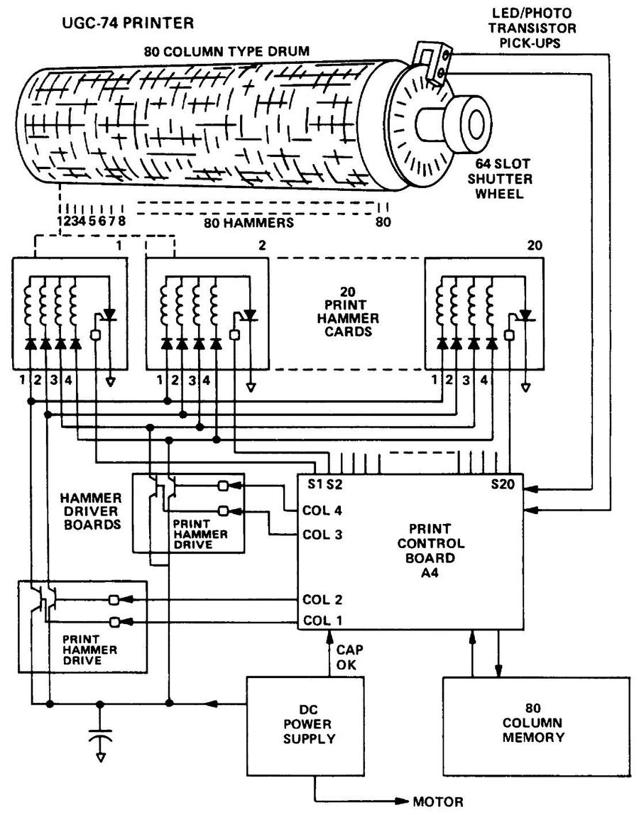
In a sense, the print control card is the heart of the printer, since it causes characters to be printed by firing hammers against the rotating drum. As the drum goes through one revolution, all 64 characters will spin past each of the 80 print positions. By firing hammers at the exact time, the card prints a line of text.9 In more detail, for each row on the drum, the printer card scans through the 80-character memory buffer using Direct Memory Access (DMA). If the value in memory matches the current drum row number, the hammer is fired. Note that the hammers don't fire simultaneously, but in sequence as memory is scanned.

This diagram shows how the print control board interacts with the rest of the system. From the Maintenance manual, TM 11-5815-602-24.

This diagram shows how the print control board interacts with the rest of the system. From the Maintenance manual, TM 11-5815-602-24.

The diagram above shows the interaction between the drum, the print control card, and the 80 hammers. The hammers are implemented on 20 print hammer cards, each with 4 hammers. Electrically, the hammers are arranged in a matrix. One wire out of 20 (S1-S20) selects the hammer board, the group of four. Another wire selects one of four hammers (Col 1-4). This approach simplifies the electronics, since 20 + 4 driver circuits and wires are used, rather than 80 (one for each column). The print control card is synchronized to the drum by two photo-transistor sensors that detect the drum's position. One sensor is triggered on each row, while the other sensor triggers once per revolution.

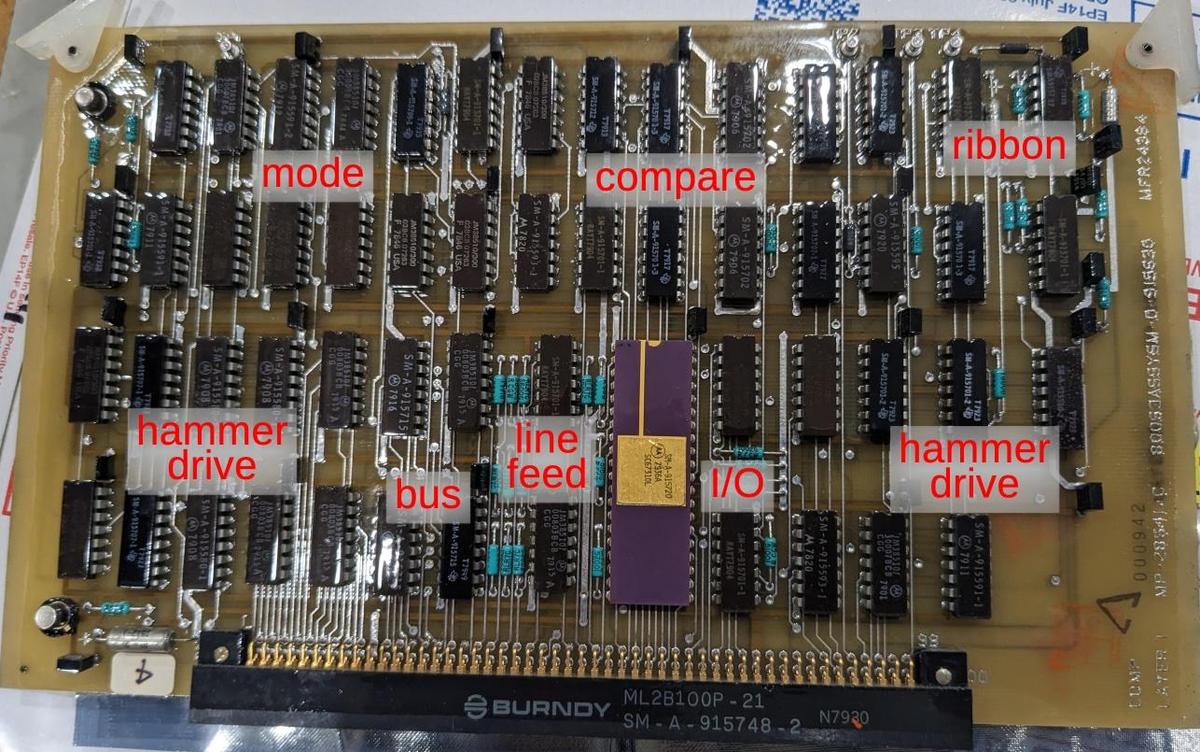
The print control card is shown below, with the main functional blocks labeled. The large purple-and-gold chip is the PIA, the same I/O chip that appeared on the CPU card. It handles a variety of signals such as the self-test request, paper out, and the drum stop signal. The mode control logic generates timing signals depending on the printer's mode. The data compare logic increments the row counter on each drum pulse, and compares the row counter to the value read from memory.10 The hammer driver circuitry on the left selects one of the 20 hammer cards, while the hammer driver circuitry on the right selects one of four hammers. The ribbon circuitry raises and lowers the ribbon so the ribbon doesn't block the text when the printer is idle. The line feed circuitry advances the paper for a line feed operation.

The print control card prints data by driving the hammers.

The print control card prints data by driving the hammers.

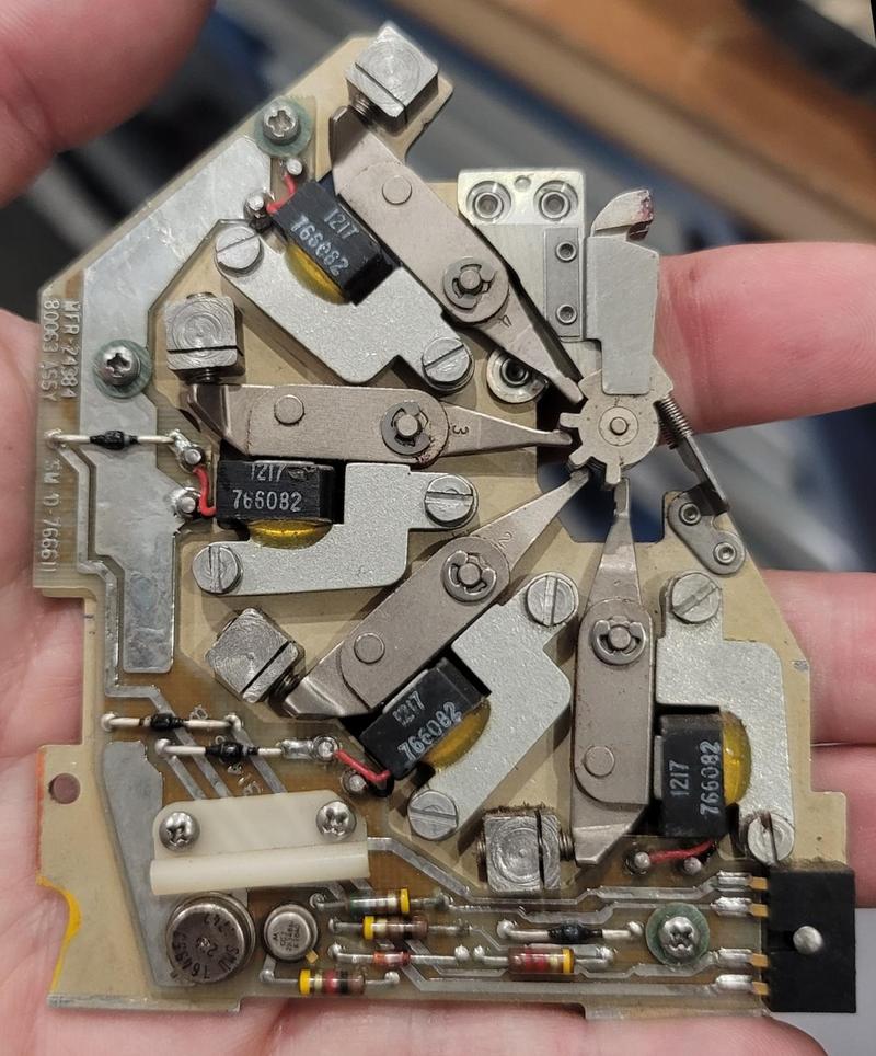
The photo below shows one of the hammer cards, with four hammers. Each hammer has an electromagnet that pulls a lever, rotating the hammer wheel, and causing the hammer to strike the paper. (The hammers themselves are in the upper right of the photo.) A screw adjustment controls the distance between each hammer and the paper, allowing precise adjustment of the timing. (Marc had to carefully adjust all the hammers to make the print quality readable.)

One of the 20 Hammer driver cards. Photo courtesy of Marcel.

One of the 20 Hammer driver cards. Photo courtesy of Marcel.

The communication card

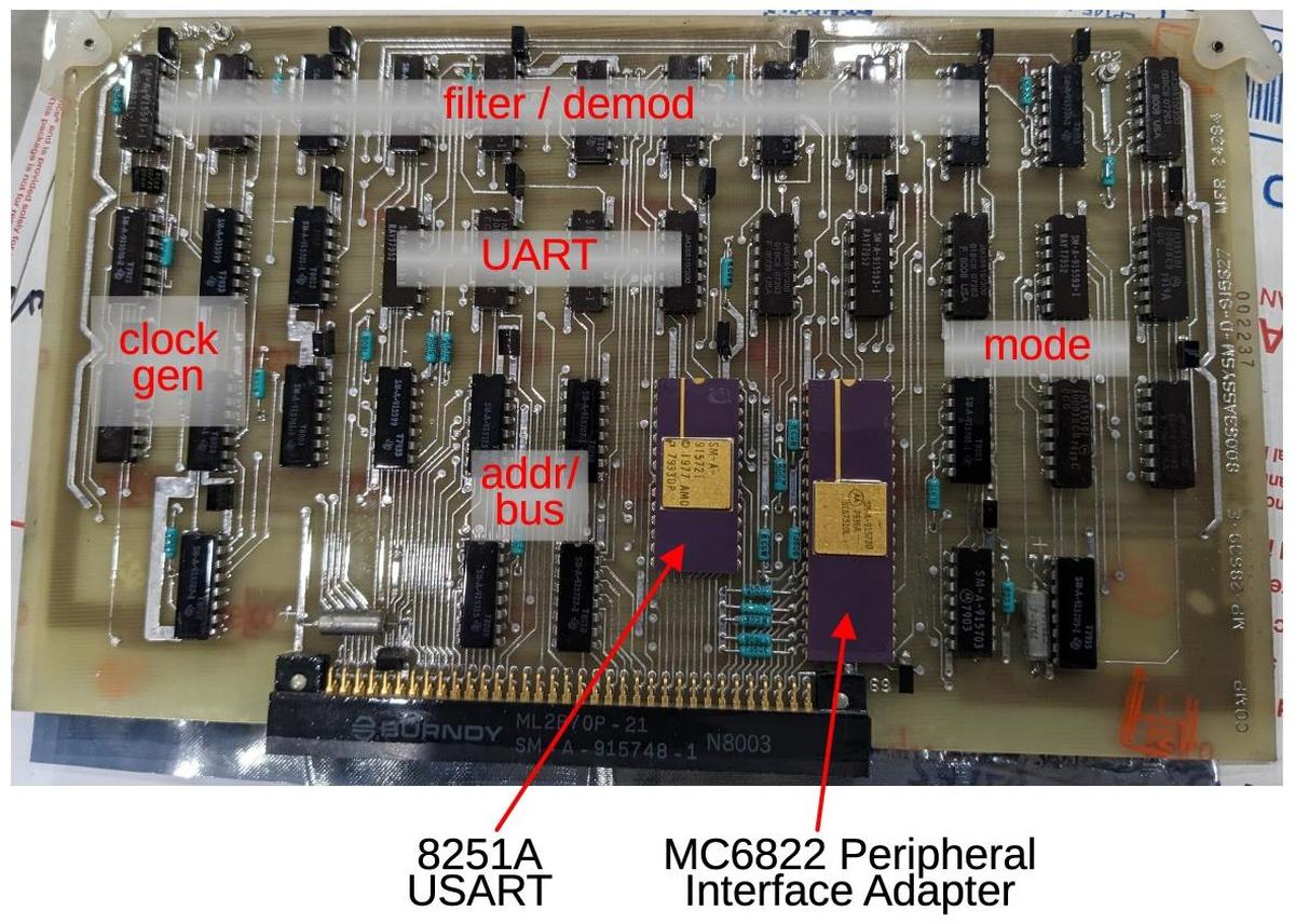
The communication card handles the teleprinter's serial data input. The key chip is the 8251A, a USART (Universal Synchronous/Asynchronous Receiver/Transmitter). This complex chip performs the conversion between the serial data stream and the bytes that the processor uses. (Note that the military teleprinter both sent and received serial data, while the Shuttle teleprinter only receives data.) The chip has a few support chips, labeled "UART" in the diagram below. The board has another Peripheral Interface Adapter chip, providing two I/O ports. These ports have functions such as reading the serial line settings (ASCII vs. Baudot, odd or even parity, number of stop bits, and current loop levels).

The communication card converts the serial input to parallel byte data.

The communication card converts the serial input to parallel byte data.

The board also has circuitry to generate the clock pulses for the selected baud rate. The mode circuitry handles various phases of transmit/receive. The filter/demod circuitry handles different input types, digitally filtering and demodulating as necessary.11

The memory card

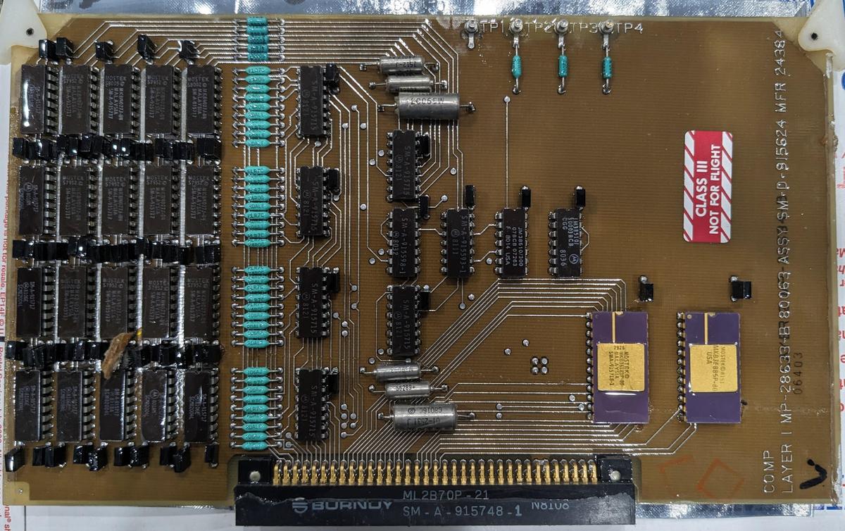
The memory card supports the word-processing feature. It provides additional RAM to hold the text buffer as well as the ROM holding the software for editing. The 16 DRAM chips on the left (MK4027) provide 8 KB of RAM while the two ROM chips on the right provide 8K of ROM. The chips in the middle to the right of the resistors split the 12 address bits into row and column addresses as required by the RAM chips. The address signals go through the numerous 24 Ω resistors in the middle; I don't know why. According to the manual, the printer operates fine without this card, except without the word processor. Since the word processor was irrelevant to the Shuttle, I wonder why this card wasn't removed to reduce weight.

The memory card has additional RAM and ROM to support the word processing feature.

The memory card has additional RAM and ROM to support the word processing feature.

The power supply

The power supply board (shown earlier) implements separate power supplies for different parts of the printer.12 The supplies are implemented as switching power supplies, which were not as common at the time as now. The microprocessor supply provides +5V, +12V, and -5V, voltages required by memory chips in the 1970s. A separate switching power supply provides +5V, -8.6V, and +8.6V for the keyboard, dustcover, and interface module, components that were removed for the Shuttle teleprinter. Another supply powers the printer's status lamps.

The drum motor supply is important because its voltage is regulated to control the rotational speed of the drum. A sensor on the drum provides a feedback pulse for each row on the drum. (I think the drum speed is 868 RPM.) These pulses control the drum motor's switching supply. If the drum spins too slowly, the voltage is increased, and similarly if it spins too fast.

The hammers have an unusual constant-current power supply. When the printer is active, this power supply generates +18 V. However, the power supply is designed to use a constant current of 600 mA regardless of the hammer activity. A capacitor provides a reservoir of power that is filled by the constant current. If the hammers are using less current, the excess current is bled off through a resistor. The purpose of this is "to mask printing intelligence during periods of message traffic." In other words, if you used a teleprinter in the embassy in Moscow, for instance, spies could monitor power transients to see when hammers are firing, and perhaps figure out what is being printed. By keeping the current constant, this source of intelligence is blocked. Of course, this feature is useless on the Space Shuttle and only wastes power.

The military teleprinter accepted multiple input voltages: 22-30 VDC, 115 VAC, or 230 VAC, along with a 12 VDC battery backup. The transformers and diodes to support these voltages were part of the interface module that was removed for the Shuttle teleprinter. Instead, the Shuttle teleprinter is powered by 28 VDC.

Mechanical changes

The military teleprinter underwent significant mechanical changes to make it suitable for the Shuttle. These changes reduced its weight from 100 pounds to 59 pounds. The most visible change to the printer is the removal of the keyboard. The entire front section of the printer was replaced, removing the controls that were not needed in the Shuttle.13 The rugged frame of the original printer was replaced with a lighter-weight (but still substantial) frame. Horizontal rails were added to the frame to support the printer in the Shuttle locker.

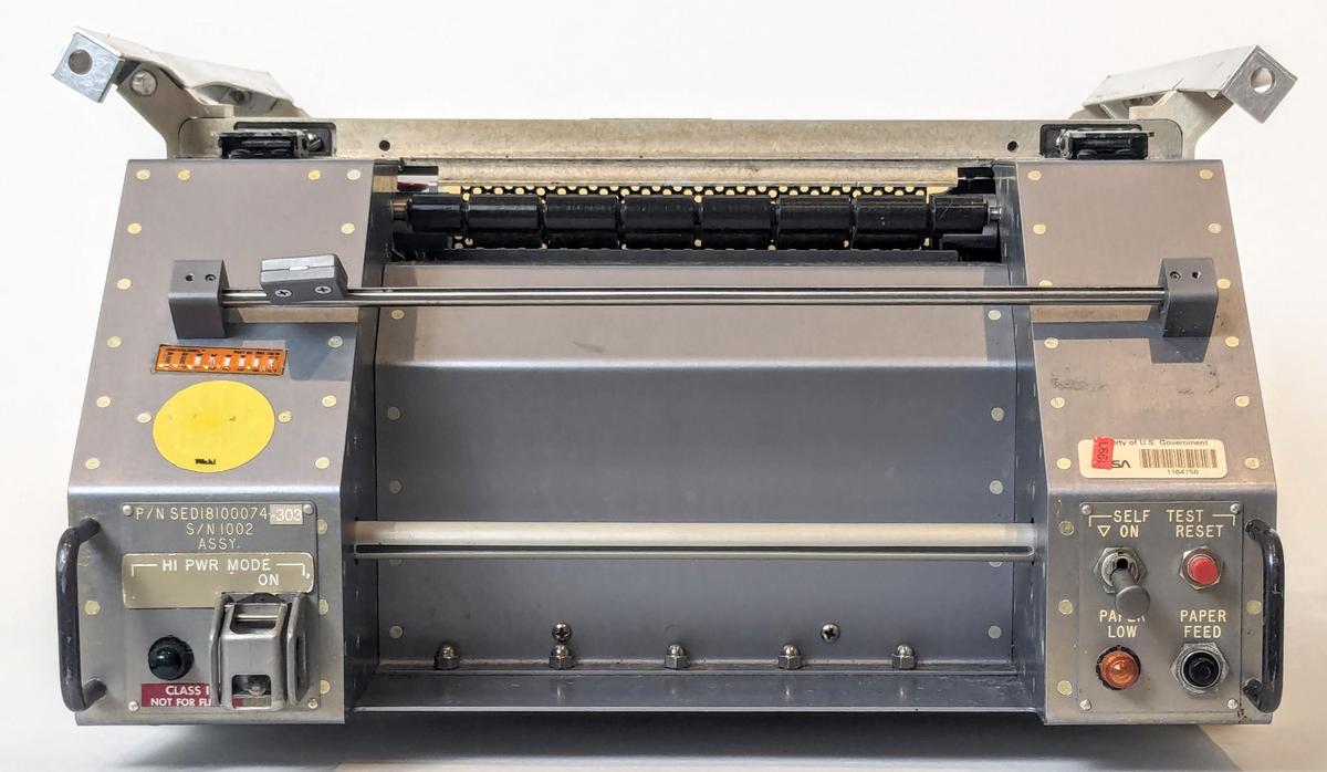
The photo below shows the front of the Shuttle teleprinter. While the military teleprinter had numerous lights and switches on the front, the Shuttle teleprinter has just two lights and four switches.

Front view of the Shuttle teleprinter. The bar across the middle holds a paper cutter for removing the output.

Front view of the Shuttle teleprinter. The bar across the middle holds a paper cutter for removing the output.

NASA was concerned that the temperature of the teleprinter could become hazardous to the astronauts. To mitigate this danger, the teleprinter had a large heat-sensitive warning sticker. The yellow sticker on the left of the teleprinter changes color and displays an image if it heats up: it shows a bandaged hand and the word "HOT". Above it is an "Omegalabel" temperature monitoring sticker that shows the highest temperature the device reached. There are more of these stickers inside the teleprinter on various motors.

The Interim Teleprinter inside the Space Shuttle

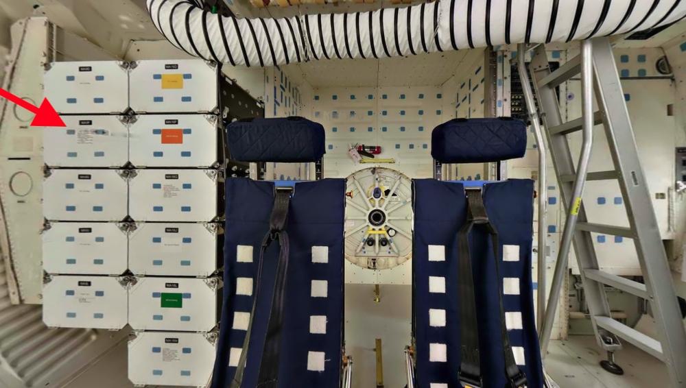
The teleprinter was too large to be mounted on the flight deck, so it was mounted in a storage locker on the middeck, one level lower. The photo below shows the location of the locker that held the teleprinter (although the teleprinter was not present in this photo), looking backward (aft) toward the airlock. The locker is denoted MA9F, indicating Mid-deck Aft, position 9F (details), in the back on the right side of the Shuttle.

This photo shows the locker that held the teleprinter. Photo by DMolybdenum, panorama viewed on renderstuff.

This photo shows the locker that held the teleprinter. Photo by DMolybdenum, panorama viewed on renderstuff.

The teleprinter was noisy because of its impact printing; even with it in a locker, the sound outside was 69.5 dB. The solution was to soundproof the locker with acoustic insulation. Various insulating materials were tested until one was found that passed the toxicity requirements. Another flammability waiver was required for the insulation.

Putting the teleprinter in an insulated locker without cooling caused another problem: overheating. The military teleprinter used 34 watts even while idle, which would cause the printer to become dangerously hot after just 6 orbits. The printer was redesigned to support a standby mode that used just 1 watt. When a signal from Earth was detected, the printer would power up while in use, and then return to standby mode. A circuit was added to send a tone back to Earth when the printer was activated, reassuring Mission Control that the printer had switched out of standby mode. These circuits were on the three custom Shuttle boards described earlier.

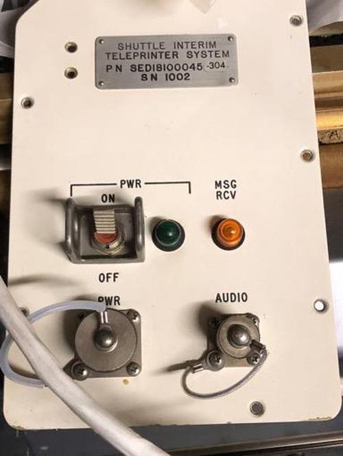
Putting the teleprinter in a locker made cabling difficult. The solution was a panel on the locker door with connectors for power and audio. The panel has a power switch and light as well as a light to indicate that a message has been received.

The panel on the outside of the locker, used for connection to the teleprinter. From distantsuns, NASA Space Flight forum.

The panel on the outside of the locker, used for connection to the teleprinter. From distantsuns, NASA Space Flight forum.

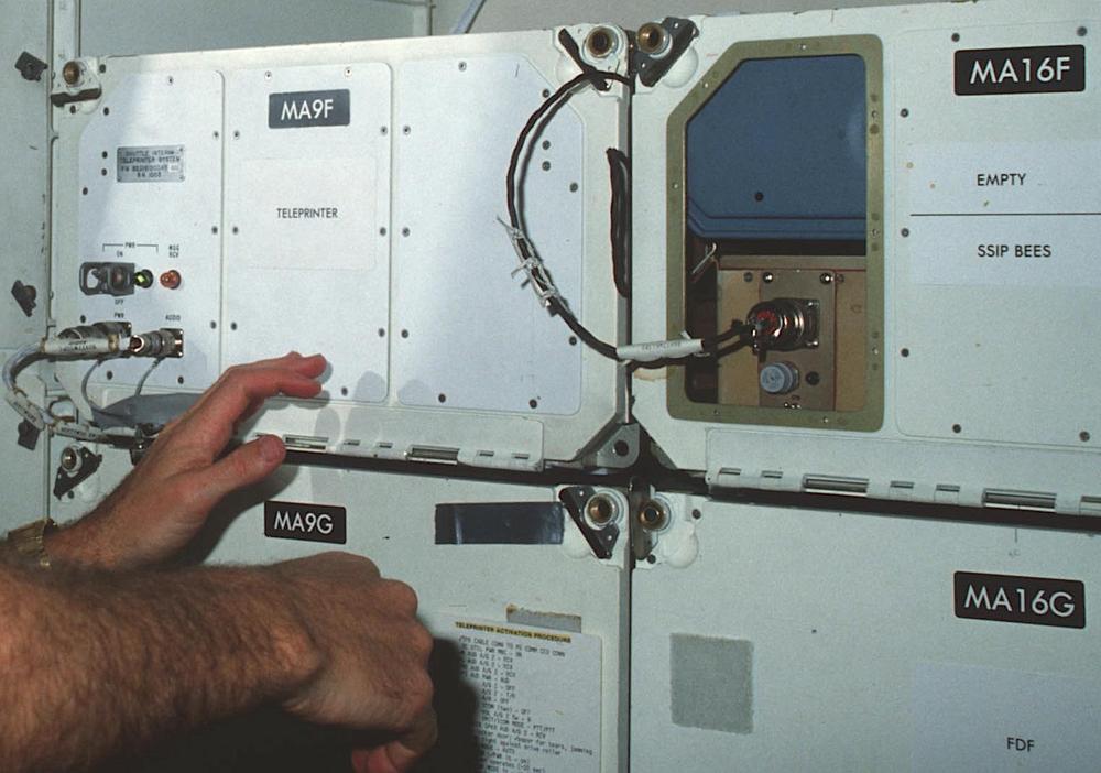
The photo below shows the teleprinter locker with the connection panel on the far left. Note the cables attached to the connectors. These cables went across the back of the Shuttle to the left side, where they went up to the flight deck; the cable routing was performed before launch.14 For this flight, the neighboring locker MA16F held 3300 honeybees for a student experiment.

The teleprinter in middeck locker MA9F on flight STS-41C.  The hands belong to mission specialist van Hoften.  From National Archives; the description says the photo is from 1995 and shows the Thermal Impulse Printer system, but both are wrong. (STS-41C was in April, 1984.)

The teleprinter in middeck locker MA9F on flight STS-41C. The hands belong to mission specialist van Hoften. From National Archives; the description says the photo is from 1995 and shows the Thermal Impulse Printer system, but both are wrong. (STS-41C was in April, 1984.)

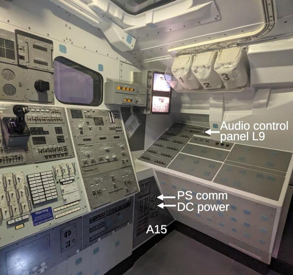
The teleprinter cables connect to the shuttle at panel A15 on the aft bulkhead of the flight deck on the left side of the Shuttle. In other words, if you sat in the Shuttle Commander's seat in the cockpit and turned around, this is what you would see.

The connections for the teleprinter in the flight deck. This photo shows Atlantis in the Kennedy Space Center visitor complex. In use, the Shuttle was much more cluttered.

The connections for the teleprinter in the flight deck. This photo shows Atlantis in the Kennedy Space Center visitor complex. In use, the Shuttle was much more cluttered.

The audio cable from the teleprinter went to the Payload Specialist communication connection on panel A15, while the power cable went to the DC power connection right below. During launch, this audio connection was needed for crew communication, so the teleprinter was plugged in after launch and the audio settings were reconfigured on panel L9. A cue card was placed above panel L9 with instructions on the teleprinter.

The teleprinter's replacements

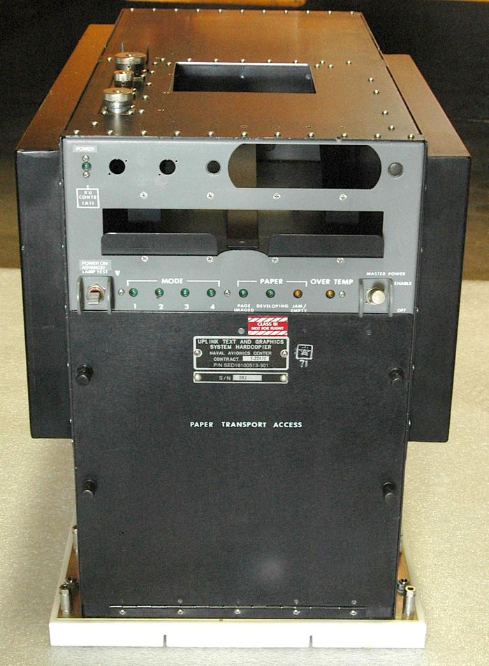
The Shuttle teleprinter was supposed to be used for a short time until the Uplink Text and Graphics System (TAGS) entered service, but things didn't work out that way. TAGS, described earlier, was the fax-like system that could receive grayscale images, but it depended on the TDRS satellites with their support for digital data. The first TDRS satellite was launched by the sixth shuttle flight, STS-6 (1983). This allowed the use of TAGS on STS-7, but the printer promptly jammed.15 TAGS had constant problems with jamming; on STS-35, the printer jammed and then the unjamming tool broke. Due to the unreliability of the TAGS, the Interim Teleprinter was kept in service as a backup device. TAGS was mounted on a dual cold plate in avionics bay 3 of the crew compartment middeck (details), on the other side of the airlock from the teleprinter.

The Uplink Text and Graphics System, serial number 2. Photo from Smithsonian National Air and Space Museum.

The Uplink Text and Graphics System, serial number 2. Photo from Smithsonian National Air and Space Museum.

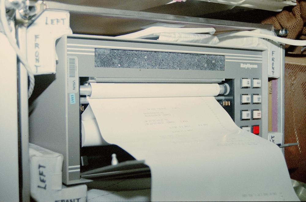
After a decade, another printer, the Thermal Impulse Printer System (TIPS) was put into service, probably on flight STS-56 in 1993. Once TIPS proved its reliability, it replaced both the teleprinter and the Text and Graphics System (TAGS). The TIPS printer was installed in mid-deck locker MF28E; the F indicates the locker was on the forward wall, not the aft wall that held the Interim Teleprinter. As a backup for the TIPS, the Shuttle flew with a second TIPS.

The Thermal Impulse Printer System (TIPS) on flight STS-58. From National Archives. The description says that this device is the teleprinter but it is TIPS.

The Thermal Impulse Printer System (TIPS) on flight STS-58. From National Archives. The description says that this device is the teleprinter but it is TIPS.

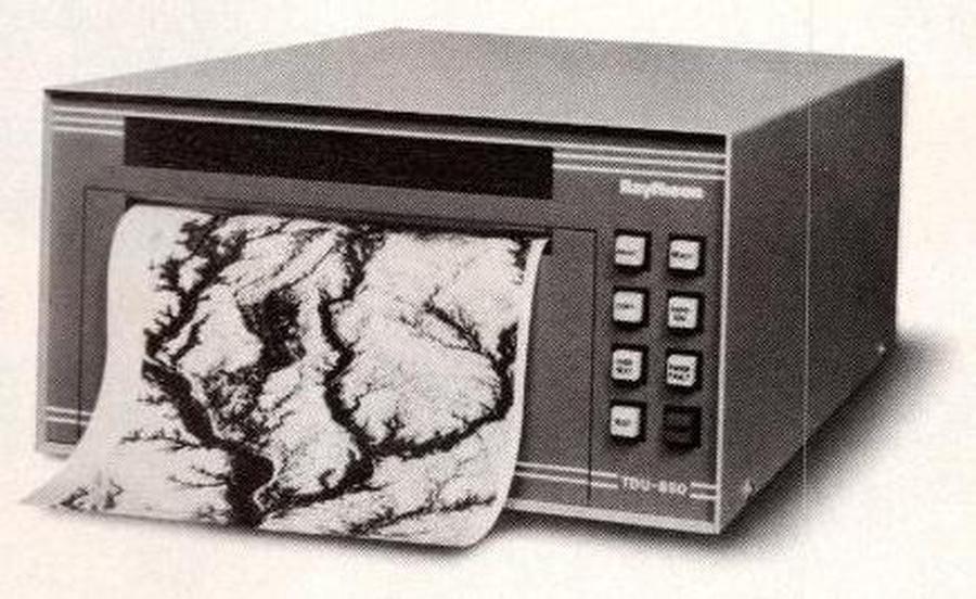
One motivation behind the TIPS thermal printer was NASA's desire to use more commercial-off-the-shelf (COTS) equipment instead of expensive custom equipment. The TIPS printer is the Raytheon TDU-850 printer (below), a commercial product that sold for $4950. A custom communication interface board inside the printer provided the interface between the printer and the Shuttle's S-Band and Ku-Band communications systems. This interface also allowed astronauts to use the TIPS as a printer for an onboard personal computer.

The Raytheon TDU-850 printer (Thermal Display Unit). From EDN, Mar 17, 1988, p.251.

The Raytheon TDU-850 printer (Thermal Display Unit). From EDN, Mar 17, 1988, p.251.

The photo below shows the TIPS printer in use, printing a long stream of output that Eileen Collins is reading. Collins was the first woman to pilot the Space Shuttle; she flew on the Shuttle four times, twice as pilot and twice as commander.

Pilot Collins reading output from the TIPS printer, the gray box on the right. This is flight STS-84, Atlantis. Photo from National Archives.

Pilot Collins reading output from the TIPS printer, the gray box on the right. This is flight STS-84, Atlantis. Photo from National Archives.

The teleprinter, operational

We succeeded in making the Shuttle teleprinter operational. The printer had many mechanical problems, mainly because the rubber rollers had turned to liquid and gummed up the mechanism. Marc disassembled the printer, carefully cleaned the mechanism, and realigned everything. I won't discuss the restoration process here since there will be a video on CuriousMarc's channel. We were able to send FSK-modulated data to the printer and it was printed successfully, as shown below.

Conclusions

At first, I thought that the Shuttle's Interim Teleprinter was a terrible design. It's absurdly heavy and was in danger of overheating. Although the design started with an existing product, much of it required redesign: the front section, the new drum, the interface, and even the frame. The design inherited features it couldn't use, such as the built-in word processor. And the constant-current feature was pointless for the Shuttle and just wasted power.

When I learned that the design had to be completed in just seven months, my opinion of the teleprinter improved. Moreover, the design had many constraints, such as toxicity and flammability restrictions, that limited the potential approaches.

In the end, the teleprinter was used on over 50 flights, acting as a reliable backup to the somewhat flaky Text and Graphics System (TAGS).16 Despite its name, the Interim Teleprinter turned out to be a long-lasting solution, not interim at all. So I have to conclude that the teleprinter was a good design, working much better and much longer than intended.17

In any case, the Interim Teleprinter is an interesting piece of hardware and I hope you enjoyed this article. Follow me on Mastodon as @[email protected] or RSS. Thanks to Marcel for providing the printer. Restoration performed with CuriousMarc, Eric Schlapefer, and Mike Stewart.

Notes and references

  1. References for the teleprinter:
    The Interim Teleprinter and its development is described in detail in: M.D. Schuette, “Space Shuttle Interim Teleprinter System,” in Conference record: NTC ’82, Systems for the Eighties, IEEE. (I'll call this the "teleprinter paper" for short.)
    The Shuttle Crew Operations Manual has extensive information on the shuttle and some information on the teleprinter.
    The teleprinter is briefly discussed here.
    Some teleprinter information is in the "Crew Systems Equipment Workbook" via RR Auction.
    The layouts of the Shuttle panels are in Orbiter OV-102 Display and Control Panel Configuration.
    The lockers are described in Orbiter middeck/paylod standard interfaces control document.
    The manuals for the AN-UGC/74 are at RadioNerds.
    An enormous collection of Shuttle documents is at gandalfddi

  2. The teleprinter paper mentions that Shuttle had one other option for receiving hardcopy data: the Text Uplink to Mass Memory System (TUMMS). This allowed text to be displayed on a CRT and the crew could take a Polaroid photo. This was obviously an impractical solution. I couldn't find any other references to TUMMS, so TUMMS may be a proposal that wasn't implemented. 

  3. Specifically, the Shuttle teleprinter was based on the Honeywell Model AN/UGC-74A9(V)3 Communications Terminal. 

  4. The mechanism of a drum printer is similar to a chain printer such as the IBM 1403 line printer: each print position has a hammer that fires when the correct character is in that position. However, chain printers have better print quality than drum printers, due to the effect of timing errors. In a drum printer, a small timing error on a hammer will cause the character to be printed too high or too low. In a chain printer, however, a timing error will cause the character to be shifted to the left or right. Vertical mispositioning is obvious and looks terrible. Horizontal mispositioning is much less noticeable since character spacing is normally slightly variable. 

  5. To be precise, the hammer is fired 1.5 characters early due to its travel time. By the time the hammer hits the drum, the drum has rotated enough to put the desired character in place. Each hammer has a screw to adjust its distance to the drum, necessary to get the timing exact. It's amazing that this system works and doesn't produce a smudged mess. 

  6. After reverse-engineering the boards, I found a paper on the Shuttle teleprinter that specified the FSK frequencies as 1600 Hz for a 0 and 2057 Hz for a 1, different from what we used. Perhaps the frequencies were changed during development. 

  7. I created schematics of the three Shuttle-specific boards. Click an image for a larger (readable) version.

    Schematic of the input board.

    Schematic of the input board.

    Schematic of the control board.

    Schematic of the control board.

    Schematic of the output board.

    Schematic of the output board.


  8. The block diagram below shows the main functional blocks of the CPU card.

    CPU block diagram. From Maintenance Manual, TM 11-5815-602-24, p3-6

    CPU block diagram. From Maintenance Manual, TM 11-5815-602-24, p3-6


  9. I expected that a line would be printed during one drum revolution but looking at the print pattern, it appears to take multiple revolutions per line. Perhaps the printer is avoiding hammers firing too close together to minimize current spikes. Moreover, the published print speed of 60 characters per second is considerably slower than one revolution. Or perhaps the hammer pattern is randomized so spies can't listen in and determine what is being printed. I'm still investigating. 

  10. Looking at the circuitry, I think the memory buffer holds the drum row number for each position, and the print control card fires the hammer if the value matches the current row number. In contrast, the "obvious" approach would put the character values in the memory buffer and the print control card would match against the current drum character. The implemented solution puts less work on the print control card, which only needs to update the target comparison value once per line, rather than every character. However, it requires the CPU card to transform the input characters into row values. 

  11. The teleprinter accepts two types of inputs: NRZ and D10. NRZ (Non-Return to Zero) is the straightforward encoding of the serial signal as 0's or 1's. The manual doesn't define D10, but I think it is Manchester encoding, using a 01 sequence for a 0 and a 10 sequence for a 1 (or inverted). The D10 signal is self-clocking, since each bit contains a transition. The demodulation circuit converts the D10 signal into a straight bit sequence. An NRZ signal can either use an external clock or an internal clock from the baud rate generator. With the internal clock, the input is sampled four times and digitally filtered since the input may not exactly line up with the internal clock. 

  12. The power supply is explained in the Maintenance Manual. The fold-out power supply schematics in that manual were not scanned for some reason but can be found in the B&C Maintenance Manual

  13. The military teleprinter contained a large interface module at the back, providing the signal and power connections to the terminal. The serial-line signals could be a 20-milliamp current loop, a 60-milliamp current loop, or MIL-STD-188/144 (similar to RS-422). The interface module converts these signals to the TTL signals used internally. The interface module also contains a power supply for the interface circuitry. Since this interfacing was not required for the Shuttle, the interface module was discarded and replaced with the Shuttle's custom FSK interface cards. The AC power supply and filtering was also removed. 

  14. I was a bit surprised that the teleprinter cables would run for a long distance through the Shuttle. But the Shuttle is full of wires and cables running in all directions, as shown in the photo below. This photo is from the same angle as the earlier diagram showing where the teleprinter is connected. This flight was after the teleprinter was retired, but the teleprinter would have been plugged in behind the exercise equipment.

    The aft flight deck of Discovery during STS-116. From National Archives.

    The aft flight deck of Discovery during STS-116. From National Archives.


  15. One source says that the inaugural flight of TAGS was STS-29 (March 1989). Another source says that testing of the "new" TAGS system continued on STS-29. Contradicting this, TAGS was used on STS-7 (June 1983), jamming after the first page. TAGS was also used on STS-8 (August 1983) but failed after five pages. The TAGS unit was not flown on STS-41B (Feb 1984, the next Challenger flight after STS-8). (Note that STS-41B was the tenth flight, considerably before STS-29, the 28th flight. The Space Shuttle mission numbers are a mess.) It's hard to reconcile these statements. Probably, TAGS was still in the testing stage as late as STS-29 due to reliability problems. 

  16. The teleprinter had a few problems during use. On flight STS-6, the teleprinter got stuck in high power mode. On flight STS-30, messages were illegible (link). 

  17. The teleprinter shows the risk of building an interim solution that turns out to last much longer than expected. This also happened with the Interim Upper Stage (IUS), a launch system to boost Shuttle payloads to a higher orbit. The Interim Upper Stage was designed as a temporary solution until a space tug became available. Eventually, NASA realized that nothing was replacing the IUS, so it was renamed to "Inertial Upper Stage", preserving the acronym.

    I'll mention that this also happened with the 8086 processor. It was intended as an interim processor until the iAPX 432 "micro-mainframe" processor was ready. The iAPX 432 turned out to be a disaster, while the "stopgap" 8086 is still with us as the x86 architecture. 

Inside an IBM/Motorola mainframe controller chip from 1981

In this article, I look inside a chip in the IBM 3274 Control Unit.1 But before I discuss the chip, I need to give some background on mainframes. (I didn't completely analyze the chip, so don't expect a nice narrative or solid conclusions.)

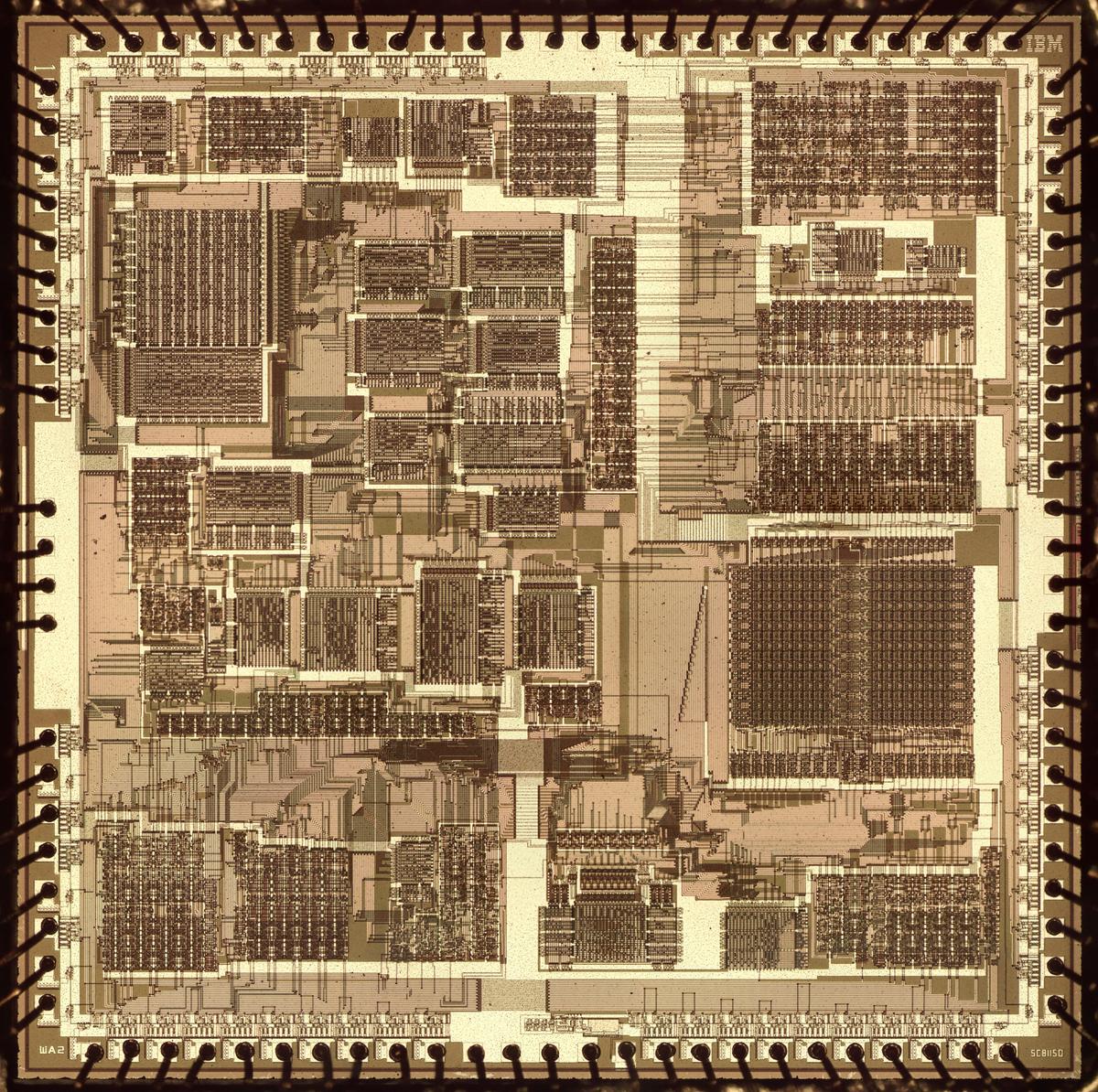
Die photo of the Motorola/IBM SC81150 chip. Click this image (or any other) for a larger version.

Die photo of the Motorola/IBM SC81150 chip. Click this image (or any other) for a larger version.

IBM's vintage mainframes were extremely underpowered compared to modern computers; a System/370 mainframe ran well under 1 million instructions per second, while a modern laptop executes billions of instructions per second. But these mainframes could support rooms full of users, while my 2017 laptop can barely handle one person.2 Mainframes achieved their high capacity by offloading much of the data entry overhead so the mainframe could focus on the "important" work. The mainframe received data directly into memory in bulk over high-speed I/O channels, without needing to handle character-by-character editing. For instance, a typical data entry terminal (a "3270") let the user update fields on the screen without involving the computer. When the user had filled out the screen, pressing the "Enter" key sent the entire data record to the mainframe at once. Thus, the mainframe didn't need to process every keystroke; it only dealt with complete records. (This is also why many modern keyboards have an "Enter" key.)

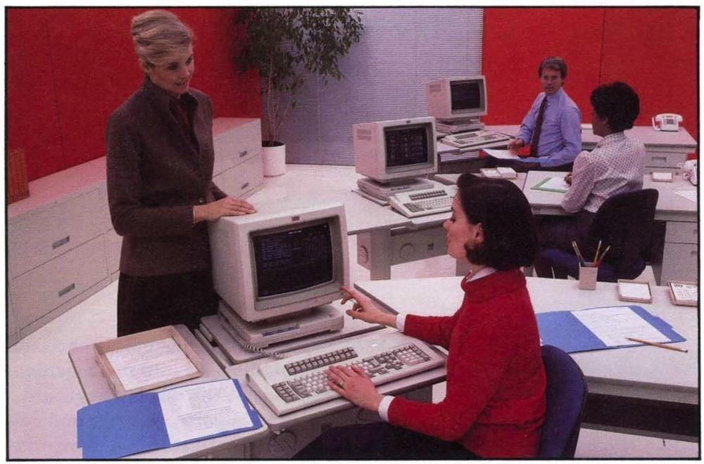
A room with IBM 3179 Color Display Stations, 1984. Note that these are terminals, not PCs. From 3270 Information Display System Introduction.

A room with IBM 3179 Color Display Stations, 1984. Note that these are terminals, not PCs. From 3270 Information Display System Introduction.

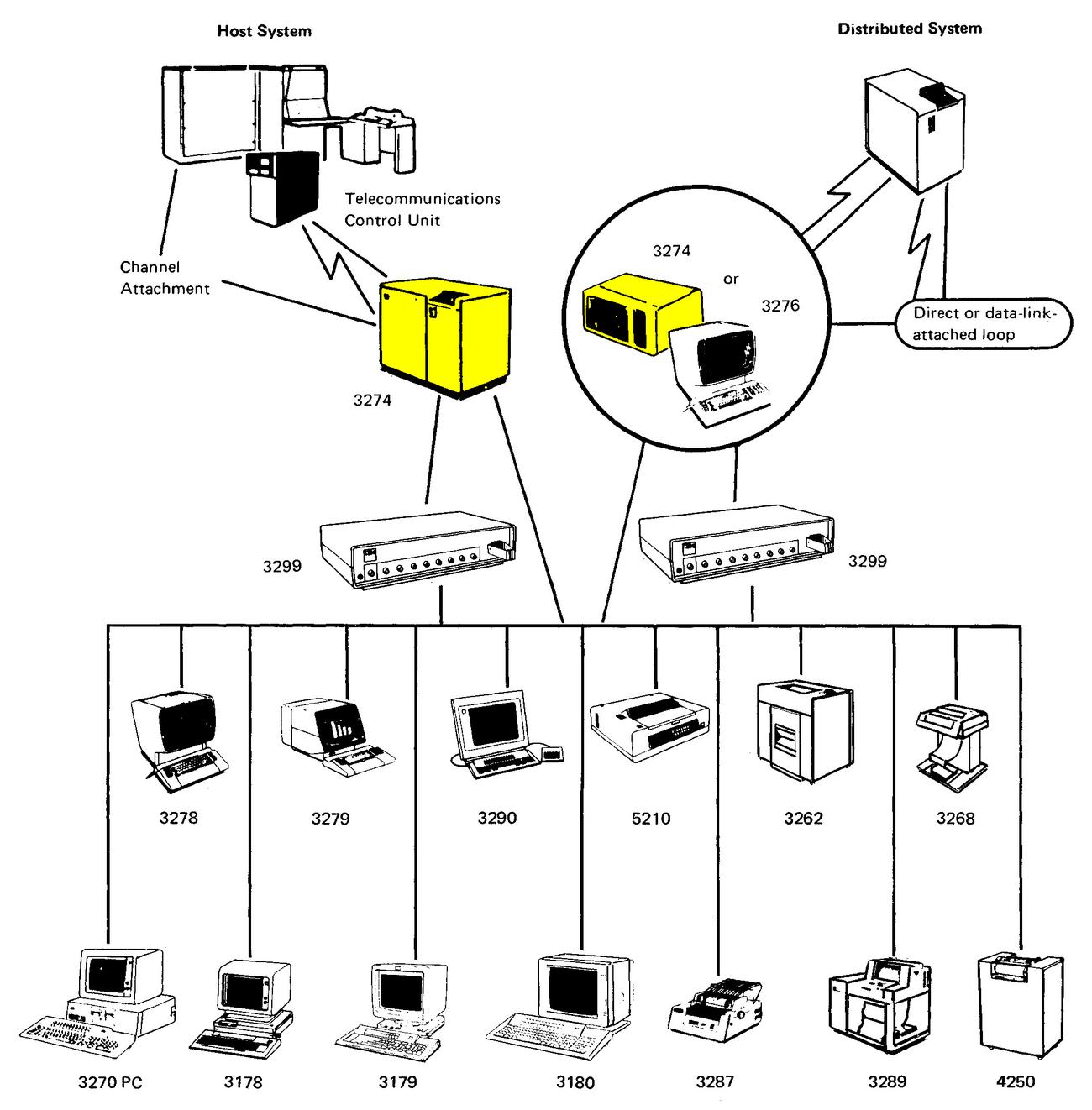
But that was just the beginning of the hierarchy of offloaded processing in a mainframe system. Terminals weren't attached directly to the mainframe. You could wire 16 terminals to a terminal multiplexer (such as the 3299). This would in turn be connected to a 3274 Control Unit that merged the terminal data and handled the network protocols. The Control Unit was connected to the mainframe's channel processor which handled I/O by moving data between memory and peripherals without slowing down the CPU. All these layers allowed the mainframe to focus on the important data processing while the layers underneath dealt with the details.3

An overview of the IBM 3270 Information Display System attachment. The yellow highlights indicate the 3274 Control Unit. From 3270 Information Display System: Introduction.

An overview of the IBM 3270 Information Display System attachment. The yellow highlights indicate the 3274 Control Unit. From 3270 Information Display System: Introduction.

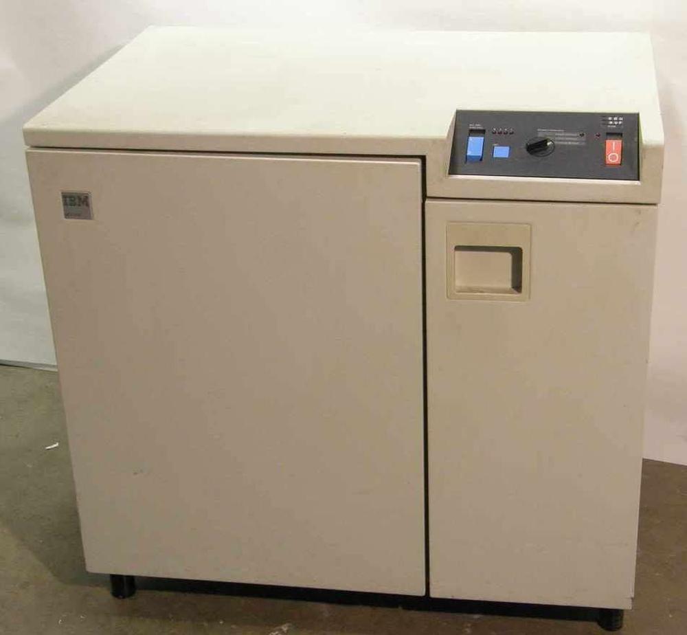
The 3274 Control Unit (highlighted above) is the source of the chip I examined. The purpose of the Control Unit "is to take care of all communication between the host system and your organization's display stations and printers". The diagram above shows how terminals were connected to a mainframe, with the 3274 Control Unit (indicated by arrows) in the middle. The 3274 was an all-purpose box, handling terminals, printers, modems, and encryption (if needed). It could communicate with the mainframe at up to 650,000 characters per second. The control unit below (above) is a boring beige box. The control panel is minimal since people normally didn't interact with the unit. On the back are coaxial connectors for the lines to the terminals, as well as connectors to interface with the computer and other peripherals.

An IBM 3274-41D Control Unit. From bitsavers.

An IBM 3274-41D Control Unit. From bitsavers.

The Keystone II board

In 1983, IBM announced new Control Unit models with twice the speed: these were the Model 41 and Model 61. These units were built around a board called Keystone II, shown below. The board is constructed with IBM's peculiar PCB style. The board is arranged as a grid of squares with the PCB traces too small to see unless you zoom in. Most of the decoupling capacitors are in IBM's thin, rectangular packages, although I see a few capacitors in more standard blue packages. IBM is almost a parallel universe with its unusual packaging for ICs and capacitors as well as the strange circuit board appearance.

The Keystone II board. The box is labeled Keystone II FCS [i.e. First Customer Shipment] July 23, 1982. Photo from bitsavers, originally from Bob Roberts.

The Keystone II board. The box is labeled Keystone II FCS [i.e. First Customer Shipment] July 23, 1982. Photo from bitsavers, originally from Bob Roberts.

Most of the chips on the board are IBM chips packaged in square aluminum cans, known as MST (Monolithic System Technology). The first line on each package is the IBM part number, which is usually undocumented. The empty socket can hold a ROS chip; ROS is Read-Only Store, known as ROM to people outside IBM. The Texas Instruments ICs in the upper right are easier to identify; the 74LS641 chips are octal bus transceivers, presumably connecting this board to the rest of the system. Similarly, the 561 5843 is a 74S240 octal bus driver while the 561 6647 chips are 74LS245 octal bus transceivers.

The memory chips on the left side of this board are interesting: each one consists of two "piggybacked" 16-kilobit DRAM chips. IBM's part number 8279251 corresponds to the Intel 4116 chip, originally made by Mostek. With 18 piggybacked chips, the board holds 64 kilobytes of parity-protected memory.

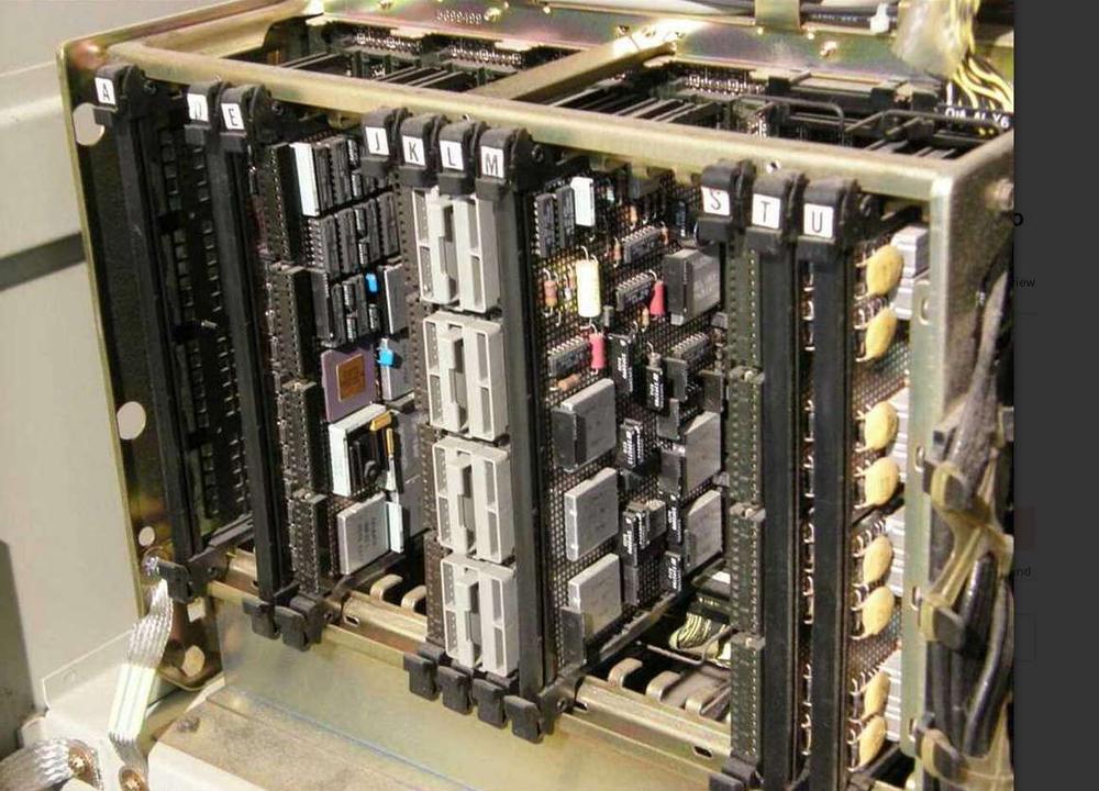
The photo below shows the Keystone II board mounted in the 3274 Control Unit. The board is in slot E towards the left and the purple Motorola IC is visible.

The Keystone II card in slot E of a 3274-41D Control Unit. Photo from bitsavers.

The Keystone II card in slot E of a 3274-41D Control Unit. Photo from bitsavers.

The Motorola/IBM chip

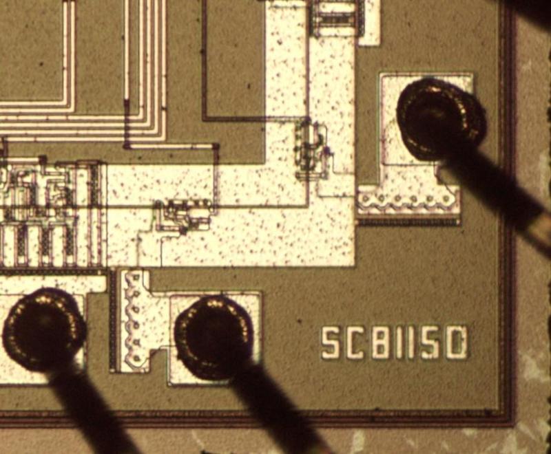
The board has a Motorola chip in a purple ceramic package; this is the chip that I examined. Popping off the golden lid reveals the silicon die underneath. The package has the part number "SC81150R", indicating a Motorola Special/Custom chip. This part number is also visible on the die, as shown below.

The corner of the die is marked with the SC81150 part number. Bond pads and bond wires are also visible.

The corner of the die is marked with the SC81150 part number. Bond pads and bond wires are also visible.

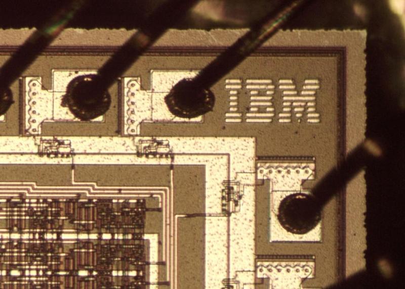
While the outside of the IC is labeled "Motorola", there are no signs of Motorola internally. Instead, the die is marked "IBM" with the eight-striped logo. My guess is that IBM designed the chip and Motorola manufactured it.

The IBM logo on the die.

The IBM logo on the die.

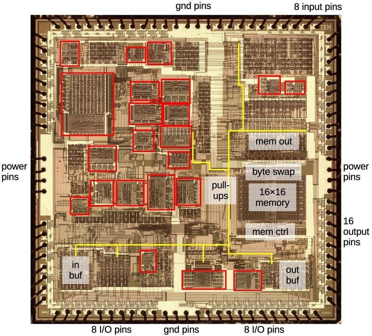
The diagram below shows the chip with some of the functional blocks identified. Around the outside are the bond pads and the bond wires that are connected to the chip's grid of pins. At the right is the 16×16 block of memory, along with its associated control, byte swap, and output circuitry. The yellowish-white lines are the metal layer on top of the chip that provides the chip's wiring. The thick metal lines distribute power and ground throughout the chip. Unlike modern chips, this chip only has a single metal layer, so power and ground distribution tends to get in the way of useful circuitry.

The die with some functional blocks identified.

The die with some functional blocks identified.

The chip is centered around a 16-bit bus (yellow line) that connects many part of the chip. To write to the bus, a circuit pulls bus lines low. The bus lines are kept high by default by 16 pull-up transistors. This approach was fairly common in the NMOS era. However, performance is limited by the relatively weak pull-up current, making bus lines slow to go high due to R-C delays. For higher performance, some chips would precharge the bus high during one clock cycle and then pull lines low during the next cycle.

The two groups of I/O pins at the bottom are connected to the input buffer on the left and the output buffer on the right. The input buffer includes XOR circuits to compute the parity of each byte. Curiously, only 6 bits of the inputs are connected to the main bus, although other circuits use all 8 bits. The buffer also has a circuit to test for a zero value, but only using 5 of the bits.

I've put red boxes around the numerous PLAs, which can be identified by their grids of transistors. This chip has an unusually large number of PLAs. Eric Schlaepfer hypothesizes that the chip was designed on a prototype circuit board using commercial PAL chips for flexibility, and then they transferred the prototype to silicon, preserving the PLA structure. I didn't see any obvious structure to the PLAs; they all seemed to have wires going all over.

The miscellaneous logic scattered around the chip includes many latches and bus drivers; the latch circuit is similar to the memory cells. I didn't fully reverse-engineer this circuitry but I didn't see anything that looked particularly interesting, such as an ALU or counter. The circuitry near the PLAs could be latches as part of state machines, but I didn't investigate further.

I was hoping to find a recognizable processor inside the package, maybe a Motorola 6809 or 68000 processor. Instead, I found a complicated chip that doesn't appear to be a processor. It has a 16×16 memory block along with about 20 PLAs (Programmable Logic Arrays), a curiously large number. PLAs are commonly used in processors for decoding instructions, since they can match bit patterns. I couldn't find a datapatch in the chip; I expected to see the ALU and registers organized in a large but regular 8-bit or 16-bit block of circuitry. The chip doesn't have any ROM4 so there's no microcode on the chip. For these reasons, I think the chip is not a processor or microcontroller, but a specialized data-handling chip, maybe using the PLAs to interpret bits of a protocol.

The chip is built with NMOS technology, the same as the 6502 and 8086 for instance, rather than CMOS technology that is used in modern chips. I measured the transistor features and the chip appears to be built with a 3.5 µm process (not nm!), which Motorola also used for the 68000 processor (1979).

The memory buffer

The chip has a 16×16 memory buffer, which could be a register file or a FIFO buffer. One interesting feature is that the buffer is triple-ported, so it can handle two reads and one write at the same time. The buffer is implemented as a grid of cells, each storing one bit. Each row corresponds to a 16-bit word, while each column corresponds to one bit in a word. Horizontal control lines (made of polysilicon) select which word gets written or read, while vertical bit lines of metal transmit each bit of the word as it is written or read.

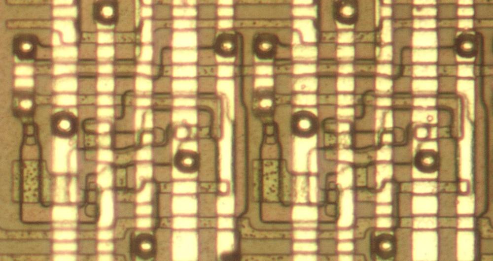
The microscope photo below shows two memory cells. These cells are repeated to create the entire memory buffer. The white vertical lines are metal wiring. The short segments are connections within a cell. The thicker vertical lines are power and ground. The thinner lines are the read and write bit lines. The silicon die itself is underneath the metal. The pinkish regions are active silicon, doped to make it conductive. The speckled golden lines are regions are polysilicon wires between the silicon and the metal. It has two roles: most importantly, when polysilicon crosses active silicon, it forms the gate of a transistor. But polysilicon is also used as wiring, important since this chip only has one layer of metal. The large, dark circles are contacts, connections between the metal layer and the silicon. Smaller square regions are contacts between silicon and polysilicon.

Two memory cells, side by side, as they appear under the microscope.

Two memory cells, side by side, as they appear under the microscope.

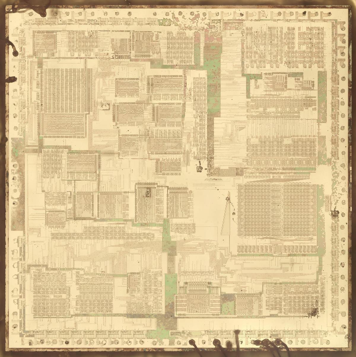
It was too difficult to interpret the circuits when they were obscured by the metal layer so I dissolved the metal layer and oxide with hydrochloric acid and Armour Etch respectively. The photo below shows the die with the metal removed; the greenish areas are remnants in areas where the metal was thick, mostly power and ground supplies. The dark regions in this image are regions of doped silicon. These are the active areas of the chip, showing the blocks of circuitry. There are also some thin lines of polysilicon wiring. The memory buffer is the large block on the right, just below the center.

The chip with the metal layer removed. Click to zoom in on the image.

The chip with the metal layer removed. Click to zoom in on the image.

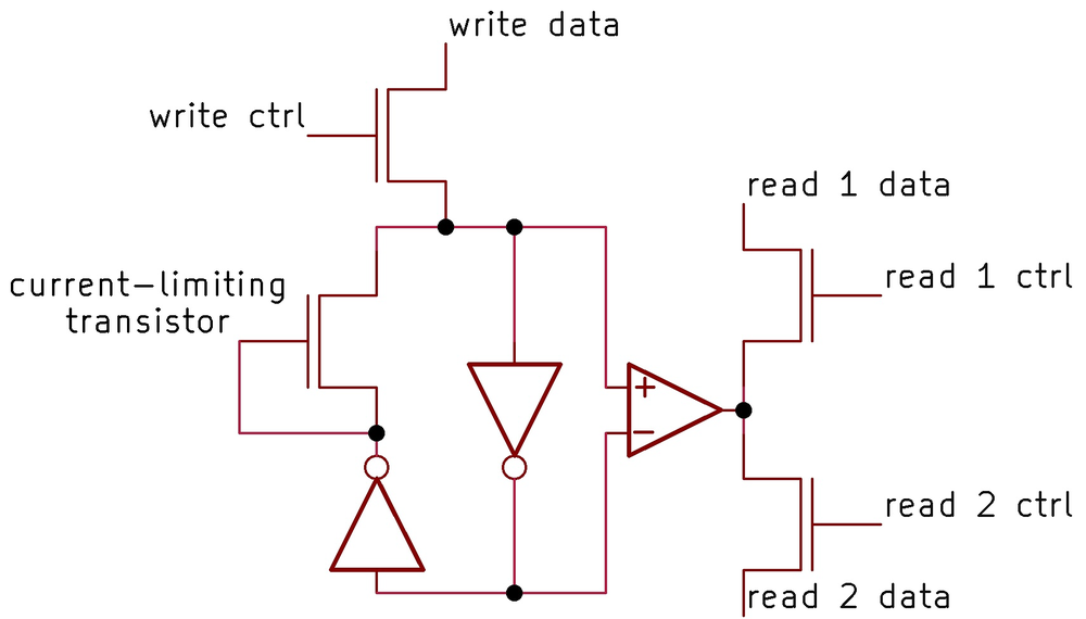
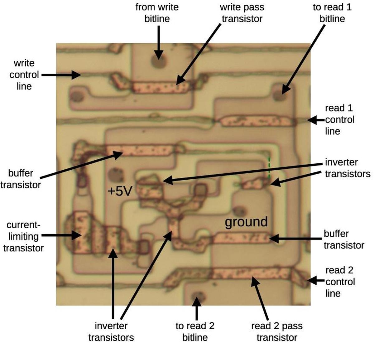
Like most implementations of static RAM, each storage cell of the buffer is implemented with cross-coupled inverters, with the output of one inverter feeding into the input of the other. To write a new value to the cell, the new value simply overpowers the inverter output, forcing the cell to the new state. To support this, one of the inverters is designed to be weak, generating a smaller signal than a regular inverter. Most circuits that I've examined create the inverter by using a weak transistor, one with a longer gate. This chip, however, uses a circuit that I haven't seen before: an additional transistor, configured to limit the current from the inverter.

The schematic below shows one cell. Each cell uses ten transistors, so it is a "10T" cell. To support multiple reads and writes, each row of cells has three horizontal control signals: one to write to the word, and two to read. Each bit position has one vertical bit line to provide the write data and two vertical bit lines for the data that is read. Pass transistors connect the bit lines to the selected cells to perform a read or a write, allowing the data to flow in or out of the cell. The symbol that looks like an op-amp is a two-transistor NMOS buffer to amplify the signal when reading the cell.

Schematic of one memory cell.

Schematic of one memory cell.

With the metal layer removed, it is easier to see the underlying silicon circuitry and reverse-engineer it. The diagram below shows the silicon and polysilicon for one storage cell, corresponding to the schematic above. (Imagine vertical metal lines for power, ground, and the three bitlines.)

One memory cell with the metal layer removed. I etched the die a few seconds too long so some of the polysilicon is very thin or missing.

One memory cell with the metal layer removed. I etched the die a few seconds too long so some of the polysilicon is very thin or missing.

The output from the memory unit contains a byte swapper. A 16-bit word is generated with the left half from the read 1 output and the second half from the read 2 output, but the bytes can be swapped. This was probably used to read an aligned 16-bit word if it was unaligned in memory.

Parity circuits

In the lower right part of the chip are two parity circuits, each computing the parity of an 8-bit input. The parity of an input is computed by XORing the bits together through a tree of 2-input XOR gates. First, four gates process pairs of input bits. Next, two XOR gates combine the outputs of the first gates. Finally, an XOR gate combines the two previous outputs to generate the final parity.

The arrangement of the 14 XOR gates to compute parity of the two 8-bit values A and B.

The arrangement of the 14 XOR gates to compute parity of the two 8-bit values A and B.

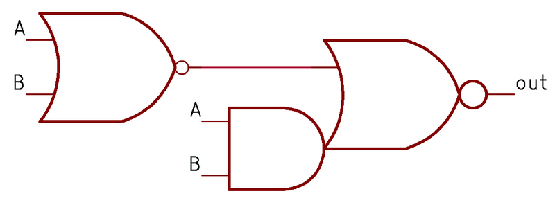
The schematic below shows how an XOR gate is built from a NOR gate and an AND-NOR gate. If both inputs are 0, the first NOR gate forces the output to 0. If both inputs are 1, the AND gate forces the output to 0. Thus, the circuit computes XOR. Each labeled block above implements the XOR circuit below.

Schematic of an XOR gate.

Schematic of an XOR gate.

Conclusion

My conclusion is that the processor for the Keystone II board is probably one of the other chips, one of the IBM metal-can MST packages, and this chip helps with data movement in some way. It would be possible to trace out the complete circuitry of the chip and determine exactly how it functions, but that is too time-consuming a project for this relatively obscure chip.

Follow me on Twitter @kenshirriff or RSS for more chip posts. I'm also on Mastodon occasionally as @[email protected]. Thanks to Al Kossow for providing the chip and Dag Spicer for providing photos. Thanks to Eric Schlaepfer for discussion.

Notes and references

  1. The 3274 Control Unit was replaced by the 3174 Establishment Controller, introduced in 1986. An "Establishment Controller" managed a cluster of peripherals or PCs connected to a host mainframe, essentially a box that provided a "kitchen-sink" of functionality including terminal support, local disk storage, Ethernet or token-ring networking, ASCII terminal support, encryption/decryption, and modem support. These units ranged from PC-sized boxes to mini-fridge-sized boxes, depending on how much functionality was required. 

  2. I'm serious that my laptop can barely handle one person; my 2017 MacBook Air starts dropping characters if it has even a moderate load, and I have to start one-finger typing. You would think that a 1.8 GHz dual-core i5 processor could handle more than 2 characters per second. I don't know if there's something wrong with it, or if modern software just has too much overhead. Don't worry, I upgraded and do most of my work on a faster, more recent laptop. 

  3. The IBM hardware model had the CPU focusing on the big picture, while the hierarchy of boxes underneath processed data, performed storage, handled printing, and so forth. In a sense, this paralleled the structure of offices in that era, where executives had assistants and secretaries to do the tedious work for them: typing, filing, and so forth. Nowadays, the computer hierarchy and the office hierarchy are both considerably flatter. Maybe there's a connection? 

  4. A ROM and a PLA are similar in many ways. The general distinction is that a ROM activates one word (row) at a time, while a PLA can activate multiple rows at a time and combine the values, giving more flexibility. A ROM generally has a binary decoder to select the row. This decoder can be recognized by its binary structure: transistors alternating by 1's, by 2's, by 4's, and so forth. 

Talking to memory: Inside the Intel 8088 processor's bus interface state machine

In 1979, Intel introduced the 8088 microprocessor, a variant of the 16-bit 8086 processor. IBM's decision to use the 8088 processor in the IBM PC (1981) was a critical point in computer history, leading to the success of the x86 architecture. The designers of the IBM PC selected the 8088 for multiple reasons, but a key factor was that the 8088 processor's 8-bit bus was similar to the bus of the 8085 processor.1 The designers were familiar with the 8085 since they had selected it for the IBM System/23 Datamaster, a now-forgotten desktop computer, making the more-powerful 8088 processor an easy choice for the IBM PC.

The 8088 processor communicates over the bus with memory and I/O devices through a highly-structured sequence of steps called "T-states." A typical 8088 bus cycle consists of four T-states, with one T-state per clock cycle. Although a four-step bus cycle may sound straightforward, its implementation uses a complicated state machine making it one of the most difficult parts of the 8088 to explain. First, the 8088 has many special cases that complicate the bus cycle. Moreover, the bus cycle is really six steps, with two undocumented "extra" steps to make bus operations more efficient. Finally, the complexity of the bus cycle is largely arbitrary, a consequence of Intel's attempts to make the 8088's bus backward-compatible with the earlier 8080 and 8085 processors. However, investigating the bus cycle circuitry in detail provides insight into the timing of the processor's instructions. In addition, this circuitry illustrates the tradeoffs and implementation decisions that are necessary in a production processor. In this blog post, I look in detail at the circuitry that implements this state machine.

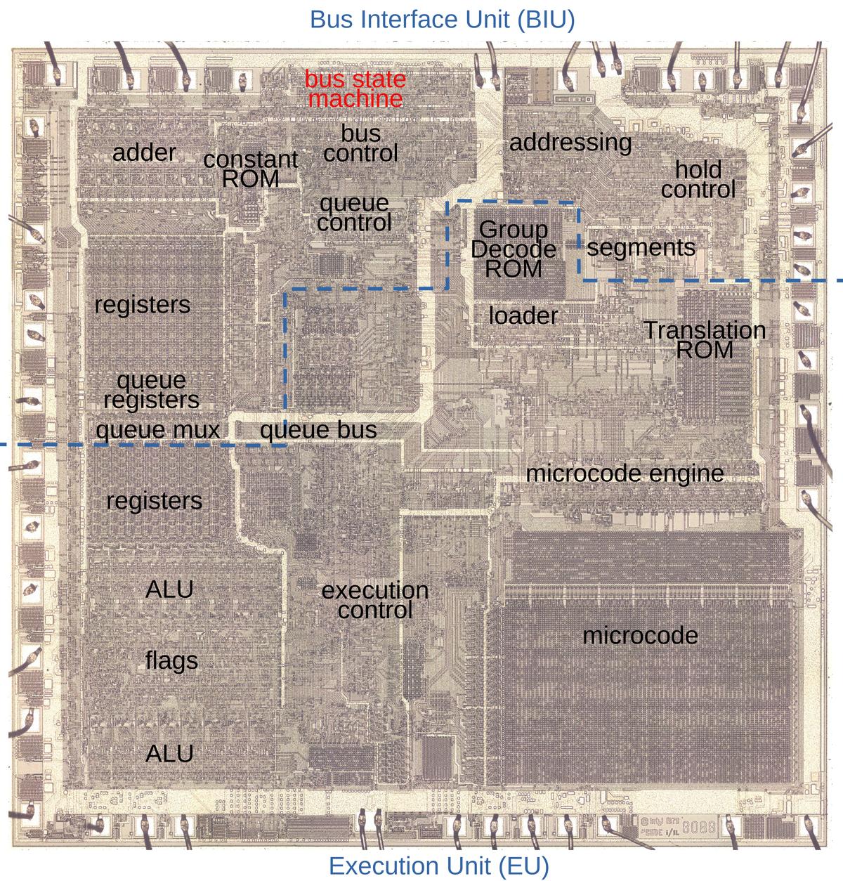
By examining the die of the 8088 microprocessor, I could reverse engineer the bus circuitry. The die photo below shows the 8088 microprocessor's silicon die under a microscope. Most visible in the photo is the metal layer on top of the chip, with the silicon and polysilicon mostly hidden underneath. Around the edges of the die, bond wires connect pads to the chip's 40 external pins. Architecturally, the chip is partitioned into a Bus Interface Unit (BIU) at the top and an Execution Unit (EU) below, with the two units running largely independently. The BIU handles bus communication (memory and I/O accesses), while the Execution Unit (EU) executes instructions. In the diagram, I've labeled the processor's key functional blocks. This article focuses on the bus state machine, highlighted in red, but other parts of the Bus Interface Unit will also play a role.

The 8088 die under a microscope, with main functional blocks labeled. This photo shows the chip's single metal layer; the polysilicon and silicon are underneath. Click on this image (or any other) for a larger version.

The 8088 die under a microscope, with main functional blocks labeled. This photo shows the chip's single metal layer; the polysilicon and silicon are underneath. Click on this image (or any other) for a larger version.

Although I'm focusing on the 8088 processor in this blog post, the 8086 is mostly the same. The 8086 and 8088 processors present the same 16-bit architecture to the programmer. The key difference is that the 8088 has an 8-bit data bus for communication with memory and I/O, rather than the 16-bit bus of the 8086. For the most part, the 8086 and 8088 are very similar internally, apart from trivial but numerous layout changes on the die. In this article, I'm focusing on the 8088 processor, but most of the description applies to the 8086 as well. Instead of constantly saying "8086/8088", I'll refer to the 8088 and try to point out places where the 8086 is different.

The bus cycle

In this section, I'll describe the basic four-step bus cycles that the 8088 performs.2 To start, the diagram below shows the states for a write cycle (slightly simplified3), when the 8088 writes to memory or an I/O device. The external bus activity is organized as four "T-states", each one clock cycle long and called T1, T2, T3, and T4, with specific actions during each state. During T1, the 8088 outputs the address on the pins. During the T2, T3, and T4 states, the 8088 outputs the data word on the same pins. The external memory or I/O device uses the T states to know when it is receiving address information or data over the bus lines.

A typical write bus cycle consists of four T states. Based on The 8086 Family Users Manual, B-16.

A typical write bus cycle consists of four T states. Based on The 8086 Family Users Manual, B-16.

For a read, the bus cycle is slightly different from the write cycle, but uses the same four T-states. During T1, the address is provided on the pins, the same as for a write. After that, however, the processor's data pins are "tri-stated" so they float electrically, allowing the external memory to put data on the bus. The processor reads the data at the end of the T3 state.

A typical read bus cycle consists of four T states. Based on The 8086 Family Users Manual, B-16.

A typical read bus cycle consists of four T states. Based on The 8086 Family Users Manual, B-16.

The purpose of the bus state machine is to move through these four T states for a read or a write. This process may seem straightforward, but (as is usually the case with the 8088) many complications make this process anything but easy. In the next sections, I'll discuss these complications. After that, I'll explain the state machine circuitry with a schematic.

Address calculation

One of the notable (if not hated) features of the 8088 processor is segmentation: the processor supports 1 megabyte of memory, but memory is partitioned into segments of 64 KB for compatibility with the earlier 8080 and 8085 processors. The 8088 calculates each 20-bit memory address by adding the value of a segment register to a 16-bit offset. This calculation is done by a dedicated address adder in the Bus Interface Unit, completely separate from the chip's ALU. (This address adder can be spotted in the upper left of the earlier die photo.)

Calculating the memory address complicates the bus cycle. As the timing diagrams above show, the processor issues the memory address during state T1 of the bus cycle. However, it takes time to perform the address calculation addition, so the address calculation must take place before T1. To accomplish this, there are two "invisible" bus states before T1; I call these states "TS" (T-start) and "T0". During these states, the Bus Interface Unit uses the address adder to compute the address, so the address will be available during the T1 state. These states are invisible to the external circuitry because they don't affect the signals from the chip.

Thus, a single memory operation takes six clock cycles: two preparatory cycles to compute the address before the four visible cycles. However, if multiple memory operations are performed, the operations are overlapped to achieve a degree of pipelining that improves performance. Specifically, the address calculation for the next memory operation takes place during the last two clock cycles of the current memory operation, saving two clock cycles. That is, for consecutive bus cycles, T3 and T4 of one bus cycle overlap with TS and T0 of the next cycle. In other words, during T3 and T4 of one bus cycle, the memory address gets computed for the next bus cycle. This pipelining significantly improves the performance of the 8088, compared to taking 6 clock cycles for each bus cycle.

With this timing, the address adder is free during cycles T1 and T2. To improve performance in another way, the 8088 uses the adder during this idle time to increment or decrement memory addresses. For instance, after popping a word from the stack, the stack pointer needs to be incremented by 2.5 Another case is block move operations (string operations), which need to increment or decrement the pointers each step. By using the address adder, the new pointer value is calculated "for free" as part of the memory cycle, without using the processors regular ALU.4

Address corrections

The address adder is used in one more context: correcting the Instruction Pointer value. Conceptually, the Instruction Pointer (or Program Counter) register points to the next instruction to execute. However, since the 8088 prefetches instructions, the Instruction Pointer indicates the next instruction to be fetched. Thus, the Instruction Pointer typically runs ahead of the "real" value. For the most part, this doesn't matter. This discrepancy becomes an issue, though, for a subroutine call, which needs to push the return address. It is also an issue for a relative branch, which jumps to an address relative to the current execution position.

To support instructions that need the next instruction address, the 8088 implements a micro-instruction CORR, which corrects the Instruction Pointer. This micro-instruction subtracts the length of the prefetch queue from the Instruction Pointer to determine the "real" Instruction Pointer. This subtraction is performed by the address adder, using correction constants that are stored in a small Constant ROM.

The tricky part is ensuring that using the address adder for correction doesn't conflict with other uses of the adder. The solution is to run a special shortened memory cycle—just the TS and T0 states—while the CORR micro-instruction is performed.6 These states block a regular memory cycle from starting, preventing a conflict over the address adder.

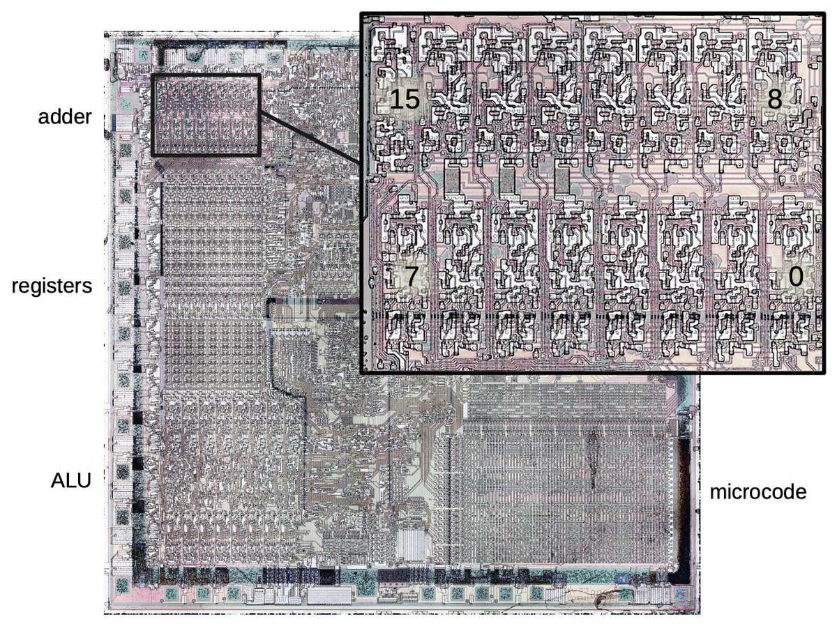
A closeup of the address adder circuitry in the 8086. From my article on the adder.

A closeup of the address adder circuitry in the 8086. From my article on the adder.

Prefetching

The 8088 prefetches instructions before they are needed, loading instructions from memory into a 4-byte prefetch queue. Prefetching usually improves performance, but can result in an instruction's memory access being delayed by a prefetch, hurting overall performance. To minimize this delay, a bus request from an instruction will preempt a prefetch, even if the prefetch has gone through TS and T0. At that point, the prefetch hasn't created any bus activity yet (which first happens in T1), so preempting the prefetch can be done cleanly. To preempt the prefetch, the bus cycle state machine jumps back to TS, skipping over T1 through T4, and starting the desired access.

A prefetch will also be preempted by the micro-instruction that stops prefetching (SUSP) or the micro-instruction that corrects addresses (CORR). In these cases, there is no point in completing the prefetch, so the state machine cycle will end with T0.

Wait states

One problem with memory accesses is that the memory may be slower than the system's clock speed, a characteristic of less-expensive memory chips. The solution in the 1970s was "wait states". If the memory couldn't respond fast enough, it would tell the processor to add idle clock cycles called wait states, until the memory could respond.7 To produce a wait state, the memory (or I/O device) lowers the processor's READY pin until it is ready to proceed. During this time, the Bus Interface Unit waits, although the Execution Unit continues operation if possible. Although Intel's documentation gives the wait cycle a separate name (Tw), internally the wait is implemented by repeating the T3 state as long as the READY pin is not active.

Halts

Another complication is that the 8088 has a HALT instruction that halts program execution until an interrupt comes in. One consequence is that HALT stops bus operations (specifically prefetching, since stopping execution will automatically stop instruction-driven bus operations). A complication is that the 8088 indicates the HALT state to external devices by performing a special T1 bus cycle without any following bus cycles. But wait: there's another complication. External devices can take control of the bus through the HOLD functionality, allowing external devices to perform operations such as DMA (Direct Memory Access). When the device ends the HOLD, the 8088 performs another special T1 bus cycle, indicating that the HALT is still in effect. Thus, the bus state machine must generate these special T1 states based on HALT and HOLD actions. (I discussed the HALT process in detail here.)

Putting it all together: the state diagram

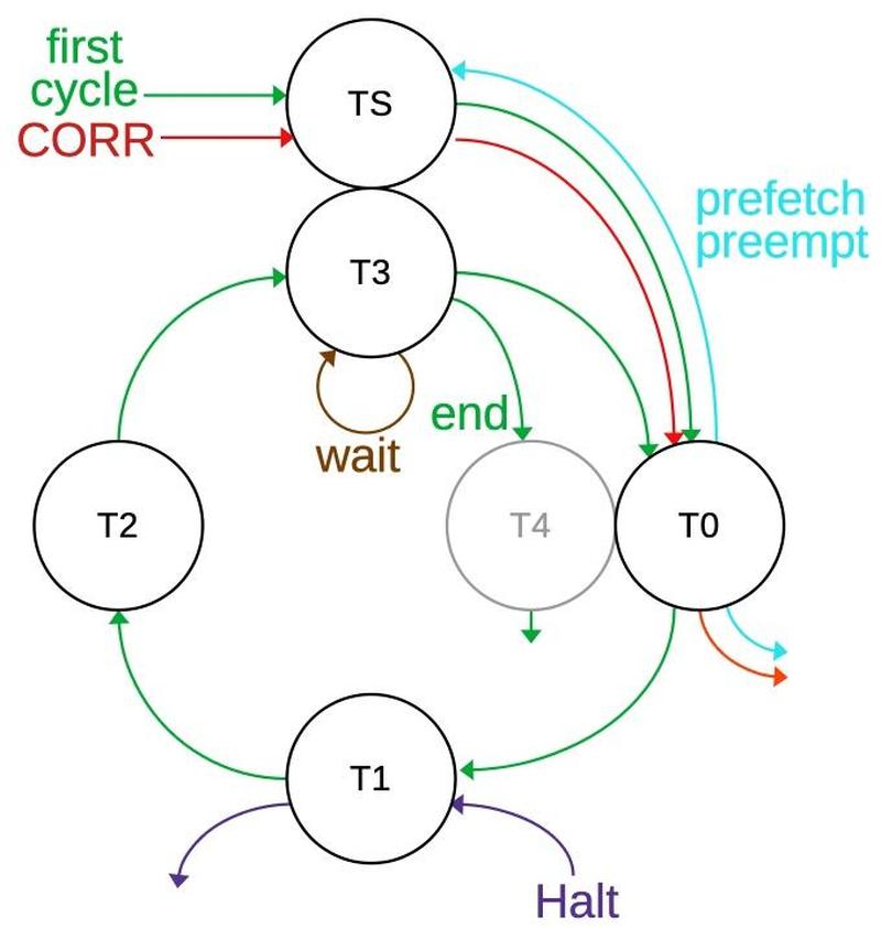
The state diagram below summarizes the different types of bus cycles. Each circle indicates a specific T-state, and the arrows indicate the transitions between states. The green line shows the basic bus cycle or cycles, starting in TS and then going around the cycle. From T3, a new cycle can start with T0 or the cycle will end with T4. Thus, new cycles can start every four clocks, but a full cycle takes six states (counting the "invisible" TS and T0). The brown line shows that the bus cycle will stay in T3 as long as there is a wait state. The red line shows the two cycles for a CORR correction, while the purple line shows the special T1 state for a HALT instruction. The cyan line shows that a prefetch cycle can be preempted after T0; the cycle will either restart at TS or end.

A state diagram showing the basic bus cycle and various complications.

A state diagram showing the basic bus cycle and various complications.

I'm showing states TS and T3 together since they overlap but aren't the same. Likewise, I'm showing T4 and T0 together. T4 is grayed out because it doesn't exist from the state machine's perspective; the circuitry doesn't take any particular action during T4.

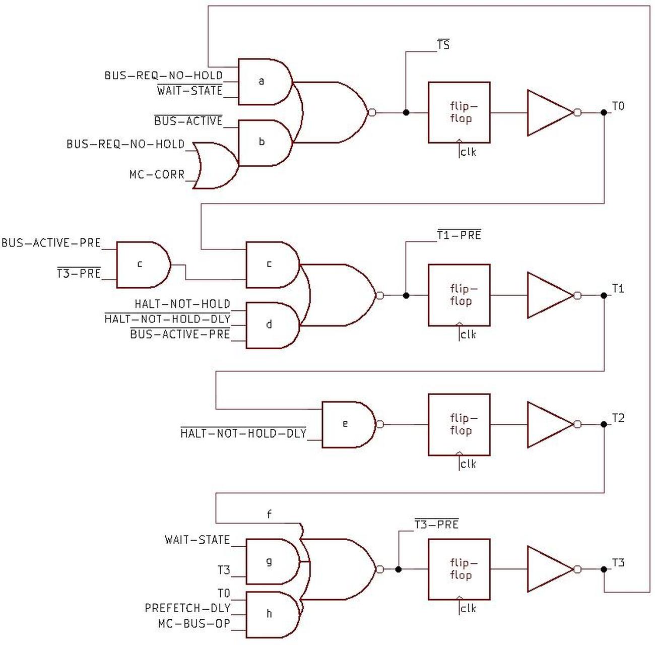
The schematic below shows the implementation of the state machine. The four flip-flops represent the four states, with one flip-flop active at a time, generating states T0, T1, T2, and T3 (from top to bottom). Each output feeds into the logic for the next state, with T3 wrapping back to the top, so the circuit moves through the states in sequence. The flip-flops are clocked so the active state will move from one flip-flop to the next according to the system clock. State TS doesn't have its own flip-flop, but is represented by the input to the T0 flip-flop, so it happens one clock cycle earlier.8 State T4 doesn't have a flip-flop since it isn't "real" to the bus state machine. The logic gates handle the special cases: blocking the state transfer if necessary or starting a state.

Schematic of the state machine.

Schematic of the state machine.

I'll explain the logic for each state in more detail. The circuitry for the TS state has two AND gates to generate new bus cycles starting from TS. The first one (a) causes TS to happen with T3 if there is a pending bus request (and no HOLD). The second AND gate (b) starts a bus cycle if the bus is not currently active and there is a bus request or a CORR micro-instruction. The flip-flop causes T0 to follow T3/TS, one clock cycle later.

The next gates (c) generate the T1 state following T0 if there is pending bus activity and the cycle isn't preempted to T3. The AND gate (d) starts the special T1 for the HALT instruction.9 The T2 state follows T1 unless T1 was generated by a HALT (e).

The T3 logic is more complicated. First, T3 will always follow T2 (f). Next, a wait state will cause T3 to remain in T3 (g). Finally, for a preempt, T3 will follow T0 (h) if there is a prefetch and a microcode bus operation (i.e. an instruction specified the bus operation).

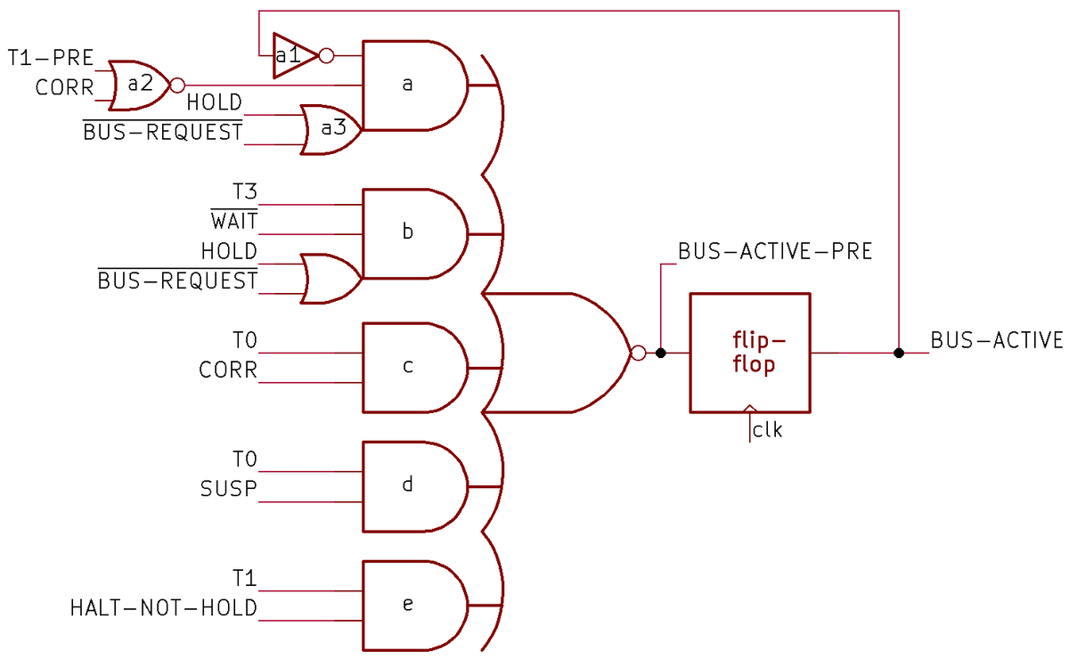
Next, I'll explain BUS-ACTIVE, an important signal that indicates if the bus is active or not. The Bus Interface Unit generates the BUS-ACTIVE signal to help control the state machine. The BUS-ACTIVE signal is also widely used in the Bus Interface Unit, controlling many functions such as transfers to and from the address registers. BUS-ACTIVE is generated by the complex circuit below that determines if the bus will be active, specifically in states T0 through T3. Because of the flip-flop, the computation of BUS-ACTIVE happens in the previous clock cycle.

The circuit to determine if the bus will be active next cycle.

The circuit to determine if the bus will be active next cycle.

In more detail, the signal BUS-ACTIVE-PRE indicates if the bus cycle will continue or will end on the next clock cycle. Delaying this signal through the flip-flop generates BUS-ACTIVE, which indicates if the bus is currently active in states T0 through T3. The top AND gate (a) is responsible for starting a cycle or keeping a cycle going (a1). It will allow a new cycle if there is a bus request (without HOLD) (a3). It will also allow a new cycle if there is a CORR micro-instruction prior to the T1 state (even if there is a HOLD, since this "fake" cycle won't use the bus) (a2). Finally, it allows a new cycle for a HALT, using T1-pre (a2).10 Next are the special cases that end a bus cycle. The second AND gate (b) ends the bus cycle after T3 unless there is a wait state or another bus request. (But a HOLD will block the next bus request.) The remaining gates end the cycle after T0 to preempt a prefetch if a CORR or SUSP micro-instruction occurs (d), or end after T1 for a HALT (e).

The BUS-ACTIVE circuit above uses a complex gate, a 5-input NOR gate fed by 5 AND gates with two attached OR gates. Surprisingly, this is implemented in the processor as a single gate with 14 inputs. Due to how gates are implemented with NMOS transistors, it is straightforward to implement this as a single gate. The inverter and NOR gate on the left, however, needed to be implemented separately, as they involve inversion; an NMOS gate must have a single inversion.

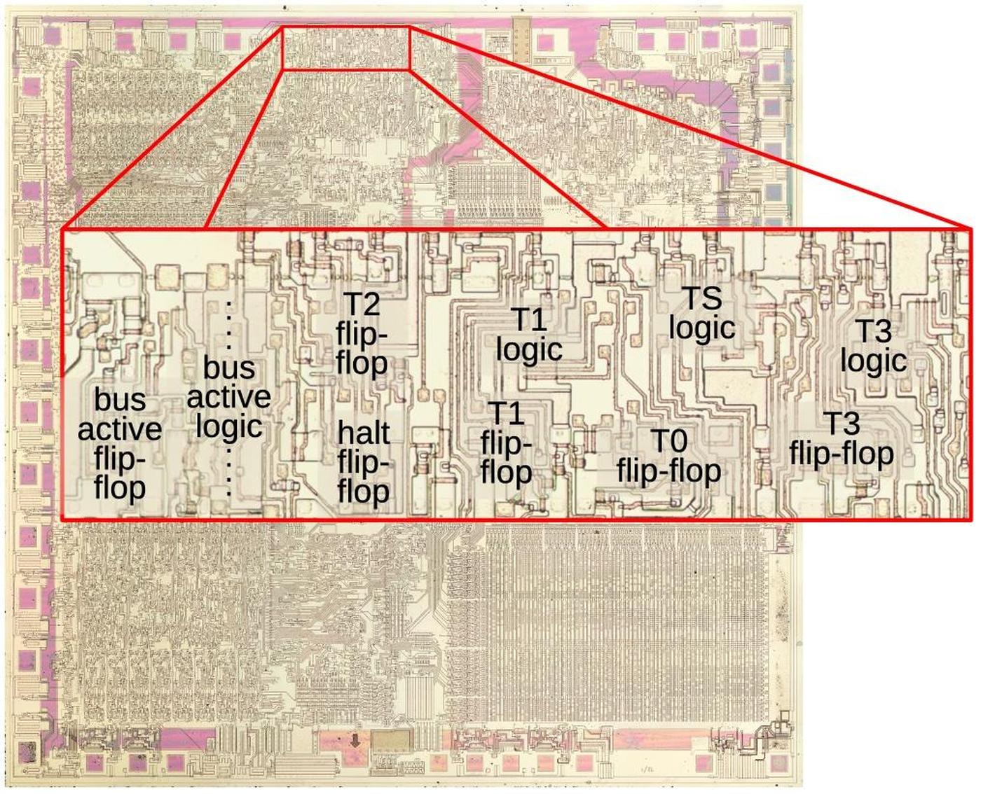
The bus state machine circuitry on the die.

The bus state machine circuitry on the die.

The diagram above shows the layout of the bus state machine circuitry on the die, zooming in on the top region of the die. The metal layer has been removed to expose the underlying silicon and polysilicon. The layout of each flip-flop is completely different, since the layout of each transistor is optimized to its surroundings. (This is in contrast to later processors such as the 386, which used standard-cell layout.) Even though the state machine consists of just a handful of flip-flops and gates, it takes a noticeable area on the die due to the large 3.2 µm feature size of the 8088. (Modern processors have features measured in nanometers, not micrometers.)

Conclusions

The bus state machine is an example of how the 8088's design consists of complications on top of complications. While the four-state bus cycle seems straightforward at first, it gets more complicated due to prefetching, wait states, the HALT instruction, and the bus hold feature, not to mention the interactions between these features. While there were good motivations behind these features, they made the processor considerably more complicated. Looking at the internals of the 8088 gives me a better understanding of why simple RISC processors became popular.

The bus state machine is a key part of the read and write circuitry, moving the bus operation through the necessary T-states. However, the state machine is not the only component in this process; a higher-level circuit decides when to perform a read, write, or prefetch, as well as breaking a 16-bit operation into two 8-bit operations.11 These circuits work together with the higher-level circuit telling the state machine when to go through the states.

In my next blog post, I'll describe the higher-level memory circuit so follow me on Twitter @kenshirriff or RSS for updates. I'm also on Mastodon as oldbytes.space@kenshirriff. If you're interested in the 8086, I wrote about the 8086 die, its die shrink process, and the 8086 registers earlier.

Notes and references

  1. The 8085 and 8088 processors both use a 4-step bus cycle for instruction fetching. For other reads and writes, the 8085's bus cycle has three steps compared to four for the 8088. Thus, the 8085 and 8088 bus cycles are similar but not an exact match. 

  2. The 8088 has separate instructions to read or write an I/O device. From the bus perspective, there's no difference between an I/O operation and a memory operation except that a pin on the chip indicates if the operation is for memory or I/O.

    The 8088 supports I/O operations for historical reasons, going back through the 8086, 8080, 8008, and the Datapoint 2200 system. In contrast, many other contemporary processors such as the 6502 used memory-mapped I/O, using standard memory accesses for I/O devices.

    The 8086 has a pin M/IO that is high for a memory access and low for an I/O access. External hardware uses this pin to determine how to handle the request. Confusingly, the pin's function is inverted on the 8088, providing IO/M. One motivation behind the 8088's 8-bit bus was to allow reuse of peripherals from the earlier 8-bit 8085 processor. Thus, the pin's function was inverted so it matched the 8085. (The pin is only available when the 8086/8088 is used in "minimum mode"; "maximum mode" remaps some of the pins, making the system more complicated but providing more control.) 

  3. I've made the timing diagram somewhat idealized so actions line up with the clock. In the real datasheet, all the signals are skewed by various amounts so the timing is more complicated. See the datasheet for pages of timing constraints on exactly when signals can change. 

  4. For more information on the implementation of the address adder, see my previous blog post

  5. The POP operation is an example of how the address adder updates a memory pointer. In this case, the stack address is moved from the Stack Pointer to the IND register in order to perform the memory read. As part of the read operation, the IND register is incremented by 2. The address is then moved from the IND register to the Stack Pointer. Thus, the address adder not only performs the segment arithmetic, but also computes the new value for the SP register.

    Note that the increment/decrement of the IND register happens after the memory operation. For stack operations, the SP must be decremented before a PUSH and incremented after a POP. The adder cannot perform a predecrement, so the PUSH instruction uses the ALU (Arithmetic/Logic Unit) to perform the decrement. 

  6. During the CORR micro-instruction, the Bus Interface Unit performs special TS and T0 states. Note that these states don't have any external effect, so they are invisible outside the processor. 

  7. The tradeoff with memory boards was that slower RAM chips were cheaper. The better RAM boards advertised "no wait states", but cheaper boards would add one or more wait states to every access, reducing performance. 

  8. Only the second half of the TS state has an effect on the Bus Interface Unit, so TS is not a full state like the other states. Specifically, a delayed TS signal is taken from the first half of the T0 flip-flop, and this signal is used to control various actions in the Bus Interface Unit. (Alternatively, you could think of this as an early T0 state.) This is why there isn't a separate flip-flop for the TS state. I suspect this is due to timing issues; by the time the TS state is generated by the logic, there isn't enough time to do anything with the state in that half clock cycle, due to propagation delays. 

  9. There is a bit more circuitry for the T1 state for a HALT. Specifically, there is a flip-flop that is set on this signal. On the next cycle, this flip-flop both blocks the generation of another T1 state and blocks the previous T1 state from progressing to T2. In other words, this flip-flop makes sure the special T1 lasts for one cycle. However, a HOLD state resets this flip-flop. That allows another special T1 to be generated when the HOLD ends. 

  10. The trickiest part of this circuit is using T1-pre to start a (short) cycle for HALT. The way it works is that the T1-pre signal only makes a difference if there isn't a bus cycle already active. The only way to get an "unexpected" T1-pre signal is if the state machine generates it for the first cycle of a HALT. Thus, the HALT triggers T1-pre and thus the bus-active signal. You might wonder why the bus-active uses this roundabout technique rather than getting triggered directly by HALT. The motivation is that the special T1 state for HALT requires the AND of three signals to ensure that the state is generated once for the HALT rather than continuously, but happens again after a HOLD, and waits until the current bus cycle is done. Instead of duplicating that AND gate, the circuit uses T1-pre which incorporates that logic. (This took me a long time to figure out.) 

  11. The 8088 has a 16-bit bus, compared to the 8088's 8-bit bus. Thus, a 16-bit bus operation on the 8088 will always require two 8-bit operations, while the 8086 can usually perform this operation in a single step. However, a 16-bit bus operation on the 8086 will still need to be broken into two 8-bit operations if the address is unaligned (i.e. odd).