Showing posts sorted by date for query 8008. Sort by relevance Show all posts

Talking to memory: Inside the Intel 8088 processor's bus interface state machine

In 1979, Intel introduced the 8088 microprocessor, a variant of the 16-bit 8086 processor. IBM's decision to use the 8088 processor in the IBM PC (1981) was a critical point in computer history, leading to the success of the x86 architecture. The designers of the IBM PC selected the 8088 for multiple reasons, but a key factor was that the 8088 processor's 8-bit bus was similar to the bus of the 8085 processor.1 The designers were familiar with the 8085 since they had selected it for the IBM System/23 Datamaster, a now-forgotten desktop computer, making the more-powerful 8088 processor an easy choice for the IBM PC.

The 8088 processor communicates over the bus with memory and I/O devices through a highly-structured sequence of steps called "T-states." A typical 8088 bus cycle consists of four T-states, with one T-state per clock cycle. Although a four-step bus cycle may sound straightforward, its implementation uses a complicated state machine making it one of the most difficult parts of the 8088 to explain. First, the 8088 has many special cases that complicate the bus cycle. Moreover, the bus cycle is really six steps, with two undocumented "extra" steps to make bus operations more efficient. Finally, the complexity of the bus cycle is largely arbitrary, a consequence of Intel's attempts to make the 8088's bus backward-compatible with the earlier 8080 and 8085 processors. However, investigating the bus cycle circuitry in detail provides insight into the timing of the processor's instructions. In addition, this circuitry illustrates the tradeoffs and implementation decisions that are necessary in a production processor. In this blog post, I look in detail at the circuitry that implements this state machine.

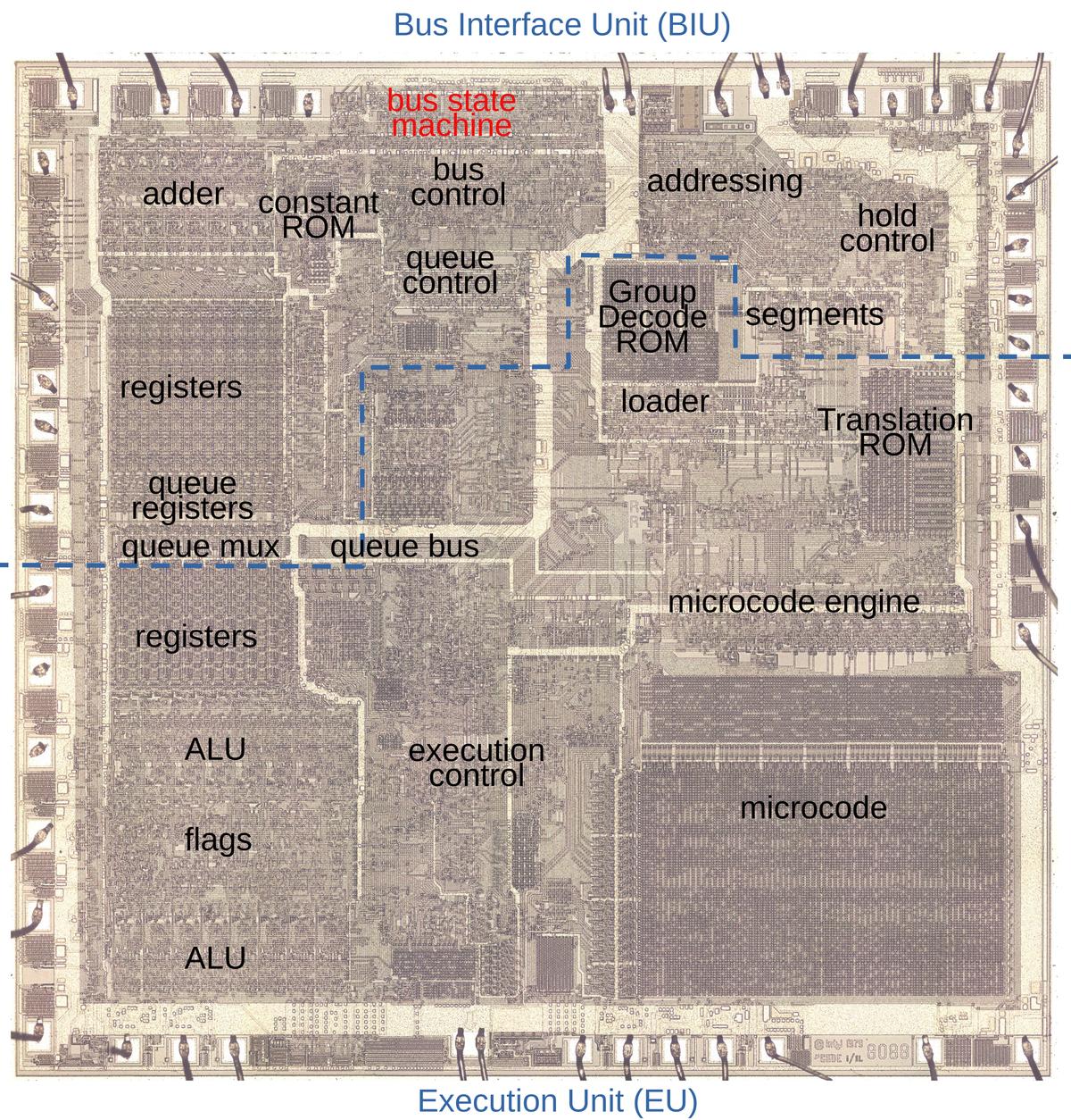
By examining the die of the 8088 microprocessor, I could reverse engineer the bus circuitry. The die photo below shows the 8088 microprocessor's silicon die under a microscope. Most visible in the photo is the metal layer on top of the chip, with the silicon and polysilicon mostly hidden underneath. Around the edges of the die, bond wires connect pads to the chip's 40 external pins. Architecturally, the chip is partitioned into a Bus Interface Unit (BIU) at the top and an Execution Unit (EU) below, with the two units running largely independently. The BIU handles bus communication (memory and I/O accesses), while the Execution Unit (EU) executes instructions. In the diagram, I've labeled the processor's key functional blocks. This article focuses on the bus state machine, highlighted in red, but other parts of the Bus Interface Unit will also play a role.

The 8088 die under a microscope, with main functional blocks labeled. This photo shows the chip's single metal layer; the polysilicon and silicon are underneath. Click on this image (or any other) for a larger version.

The 8088 die under a microscope, with main functional blocks labeled. This photo shows the chip's single metal layer; the polysilicon and silicon are underneath. Click on this image (or any other) for a larger version.

Although I'm focusing on the 8088 processor in this blog post, the 8086 is mostly the same. The 8086 and 8088 processors present the same 16-bit architecture to the programmer. The key difference is that the 8088 has an 8-bit data bus for communication with memory and I/O, rather than the 16-bit bus of the 8086. For the most part, the 8086 and 8088 are very similar internally, apart from trivial but numerous layout changes on the die. In this article, I'm focusing on the 8088 processor, but most of the description applies to the 8086 as well. Instead of constantly saying "8086/8088", I'll refer to the 8088 and try to point out places where the 8086 is different.

The bus cycle

In this section, I'll describe the basic four-step bus cycles that the 8088 performs.2 To start, the diagram below shows the states for a write cycle (slightly simplified3), when the 8088 writes to memory or an I/O device. The external bus activity is organized as four "T-states", each one clock cycle long and called T1, T2, T3, and T4, with specific actions during each state. During T1, the 8088 outputs the address on the pins. During the T2, T3, and T4 states, the 8088 outputs the data word on the same pins. The external memory or I/O device uses the T states to know when it is receiving address information or data over the bus lines.

A typical write bus cycle consists of four T states. Based on The 8086 Family Users Manual, B-16.

A typical write bus cycle consists of four T states. Based on The 8086 Family Users Manual, B-16.

For a read, the bus cycle is slightly different from the write cycle, but uses the same four T-states. During T1, the address is provided on the pins, the same as for a write. After that, however, the processor's data pins are "tri-stated" so they float electrically, allowing the external memory to put data on the bus. The processor reads the data at the end of the T3 state.

A typical read bus cycle consists of four T states. Based on The 8086 Family Users Manual, B-16.

A typical read bus cycle consists of four T states. Based on The 8086 Family Users Manual, B-16.

The purpose of the bus state machine is to move through these four T states for a read or a write. This process may seem straightforward, but (as is usually the case with the 8088) many complications make this process anything but easy. In the next sections, I'll discuss these complications. After that, I'll explain the state machine circuitry with a schematic.

Address calculation

One of the notable (if not hated) features of the 8088 processor is segmentation: the processor supports 1 megabyte of memory, but memory is partitioned into segments of 64 KB for compatibility with the earlier 8080 and 8085 processors. The 8088 calculates each 20-bit memory address by adding the value of a segment register to a 16-bit offset. This calculation is done by a dedicated address adder in the Bus Interface Unit, completely separate from the chip's ALU. (This address adder can be spotted in the upper left of the earlier die photo.)

Calculating the memory address complicates the bus cycle. As the timing diagrams above show, the processor issues the memory address during state T1 of the bus cycle. However, it takes time to perform the address calculation addition, so the address calculation must take place before T1. To accomplish this, there are two "invisible" bus states before T1; I call these states "TS" (T-start) and "T0". During these states, the Bus Interface Unit uses the address adder to compute the address, so the address will be available during the T1 state. These states are invisible to the external circuitry because they don't affect the signals from the chip.

Thus, a single memory operation takes six clock cycles: two preparatory cycles to compute the address before the four visible cycles. However, if multiple memory operations are performed, the operations are overlapped to achieve a degree of pipelining that improves performance. Specifically, the address calculation for the next memory operation takes place during the last two clock cycles of the current memory operation, saving two clock cycles. That is, for consecutive bus cycles, T3 and T4 of one bus cycle overlap with TS and T0 of the next cycle. In other words, during T3 and T4 of one bus cycle, the memory address gets computed for the next bus cycle. This pipelining significantly improves the performance of the 8088, compared to taking 6 clock cycles for each bus cycle.

With this timing, the address adder is free during cycles T1 and T2. To improve performance in another way, the 8088 uses the adder during this idle time to increment or decrement memory addresses. For instance, after popping a word from the stack, the stack pointer needs to be incremented by 2.5 Another case is block move operations (string operations), which need to increment or decrement the pointers each step. By using the address adder, the new pointer value is calculated "for free" as part of the memory cycle, without using the processors regular ALU.4

Address corrections

The address adder is used in one more context: correcting the Instruction Pointer value. Conceptually, the Instruction Pointer (or Program Counter) register points to the next instruction to execute. However, since the 8088 prefetches instructions, the Instruction Pointer indicates the next instruction to be fetched. Thus, the Instruction Pointer typically runs ahead of the "real" value. For the most part, this doesn't matter. This discrepancy becomes an issue, though, for a subroutine call, which needs to push the return address. It is also an issue for a relative branch, which jumps to an address relative to the current execution position.

To support instructions that need the next instruction address, the 8088 implements a micro-instruction CORR, which corrects the Instruction Pointer. This micro-instruction subtracts the length of the prefetch queue from the Instruction Pointer to determine the "real" Instruction Pointer. This subtraction is performed by the address adder, using correction constants that are stored in a small Constant ROM.

The tricky part is ensuring that using the address adder for correction doesn't conflict with other uses of the adder. The solution is to run a special shortened memory cycle—just the TS and T0 states—while the CORR micro-instruction is performed.6 These states block a regular memory cycle from starting, preventing a conflict over the address adder.

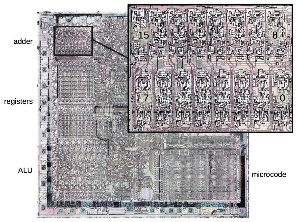
A closeup of the address adder circuitry in the 8086. From my article on the adder.

A closeup of the address adder circuitry in the 8086. From my article on the adder.

Prefetching

The 8088 prefetches instructions before they are needed, loading instructions from memory into a 4-byte prefetch queue. Prefetching usually improves performance, but can result in an instruction's memory access being delayed by a prefetch, hurting overall performance. To minimize this delay, a bus request from an instruction will preempt a prefetch, even if the prefetch has gone through TS and T0. At that point, the prefetch hasn't created any bus activity yet (which first happens in T1), so preempting the prefetch can be done cleanly. To preempt the prefetch, the bus cycle state machine jumps back to TS, skipping over T1 through T4, and starting the desired access.

A prefetch will also be preempted by the micro-instruction that stops prefetching (SUSP) or the micro-instruction that corrects addresses (CORR). In these cases, there is no point in completing the prefetch, so the state machine cycle will end with T0.

Wait states

One problem with memory accesses is that the memory may be slower than the system's clock speed, a characteristic of less-expensive memory chips. The solution in the 1970s was "wait states". If the memory couldn't respond fast enough, it would tell the processor to add idle clock cycles called wait states, until the memory could respond.7 To produce a wait state, the memory (or I/O device) lowers the processor's READY pin until it is ready to proceed. During this time, the Bus Interface Unit waits, although the Execution Unit continues operation if possible. Although Intel's documentation gives the wait cycle a separate name (Tw), internally the wait is implemented by repeating the T3 state as long as the READY pin is not active.

Halts

Another complication is that the 8088 has a HALT instruction that halts program execution until an interrupt comes in. One consequence is that HALT stops bus operations (specifically prefetching, since stopping execution will automatically stop instruction-driven bus operations). A complication is that the 8088 indicates the HALT state to external devices by performing a special T1 bus cycle without any following bus cycles. But wait: there's another complication. External devices can take control of the bus through the HOLD functionality, allowing external devices to perform operations such as DMA (Direct Memory Access). When the device ends the HOLD, the 8088 performs another special T1 bus cycle, indicating that the HALT is still in effect. Thus, the bus state machine must generate these special T1 states based on HALT and HOLD actions. (I discussed the HALT process in detail here.)

Putting it all together: the state diagram

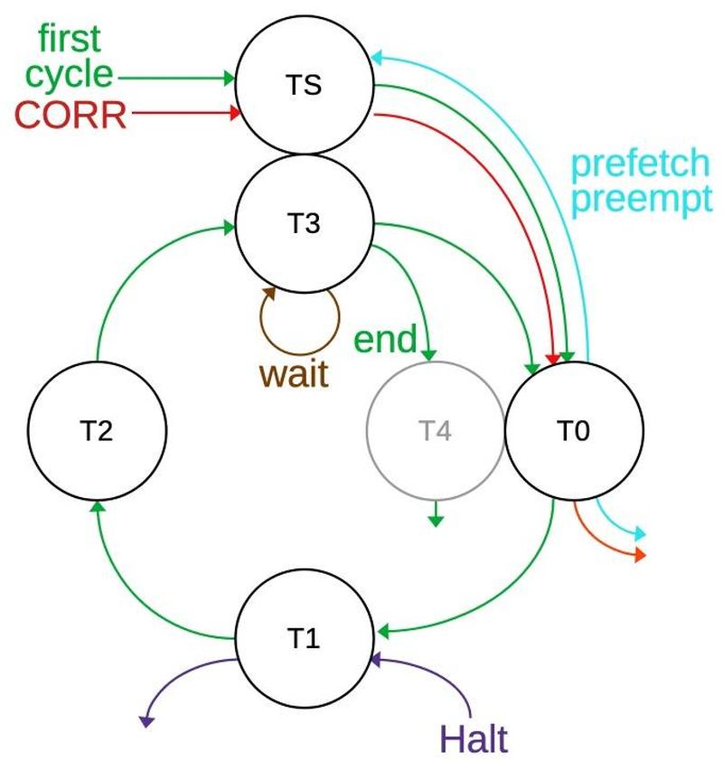
The state diagram below summarizes the different types of bus cycles. Each circle indicates a specific T-state, and the arrows indicate the transitions between states. The green line shows the basic bus cycle or cycles, starting in TS and then going around the cycle. From T3, a new cycle can start with T0 or the cycle will end with T4. Thus, new cycles can start every four clocks, but a full cycle takes six states (counting the "invisible" TS and T0). The brown line shows that the bus cycle will stay in T3 as long as there is a wait state. The red line shows the two cycles for a CORR correction, while the purple line shows the special T1 state for a HALT instruction. The cyan line shows that a prefetch cycle can be preempted after T0; the cycle will either restart at TS or end.

A state diagram showing the basic bus cycle and various complications.

A state diagram showing the basic bus cycle and various complications.

I'm showing states TS and T3 together since they overlap but aren't the same. Likewise, I'm showing T4 and T0 together. T4 is grayed out because it doesn't exist from the state machine's perspective; the circuitry doesn't take any particular action during T4.

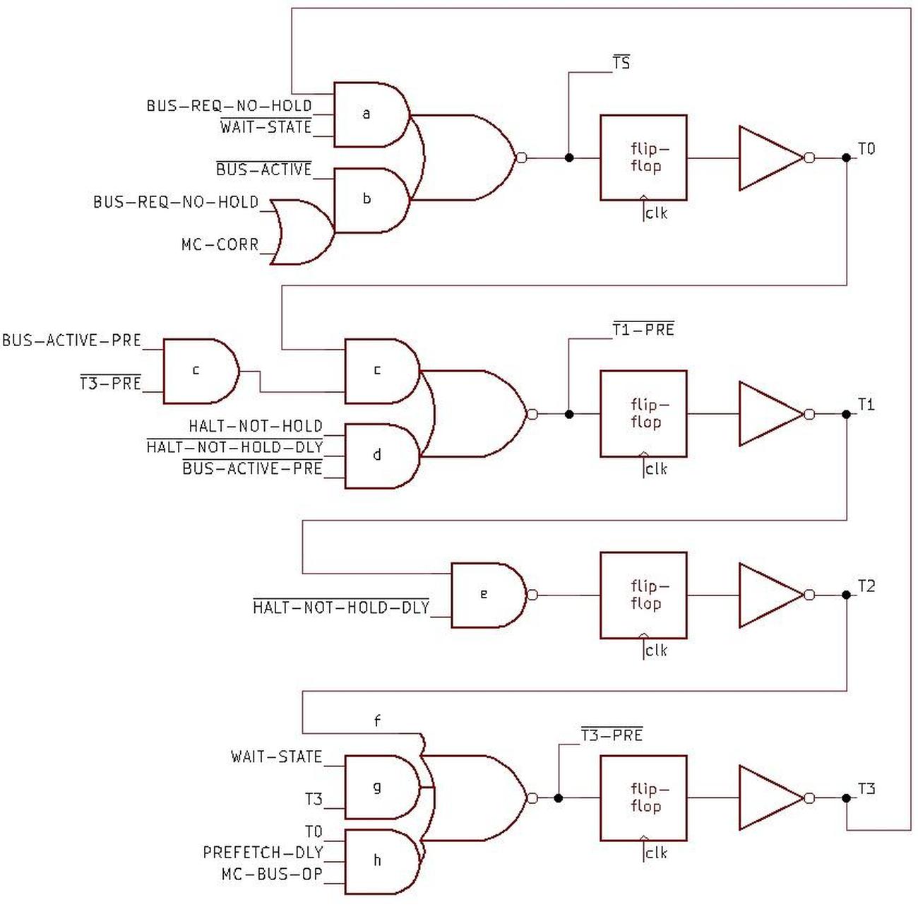
The schematic below shows the implementation of the state machine. The four flip-flops represent the four states, with one flip-flop active at a time, generating states T0, T1, T2, and T3 (from top to bottom). Each output feeds into the logic for the next state, with T3 wrapping back to the top, so the circuit moves through the states in sequence. The flip-flops are clocked so the active state will move from one flip-flop to the next according to the system clock. State TS doesn't have its own flip-flop, but is represented by the input to the T0 flip-flop, so it happens one clock cycle earlier.8 State T4 doesn't have a flip-flop since it isn't "real" to the bus state machine. The logic gates handle the special cases: blocking the state transfer if necessary or starting a state.

Schematic of the state machine.

Schematic of the state machine.

I'll explain the logic for each state in more detail. The circuitry for the TS state has two AND gates to generate new bus cycles starting from TS. The first one (a) causes TS to happen with T3 if there is a pending bus request (and no HOLD). The second AND gate (b) starts a bus cycle if the bus is not currently active and there is a bus request or a CORR micro-instruction. The flip-flop causes T0 to follow T3/TS, one clock cycle later.

The next gates (c) generate the T1 state following T0 if there is pending bus activity and the cycle isn't preempted to T3. The AND gate (d) starts the special T1 for the HALT instruction.9 The T2 state follows T1 unless T1 was generated by a HALT (e).

The T3 logic is more complicated. First, T3 will always follow T2 (f). Next, a wait state will cause T3 to remain in T3 (g). Finally, for a preempt, T3 will follow T0 (h) if there is a prefetch and a microcode bus operation (i.e. an instruction specified the bus operation).

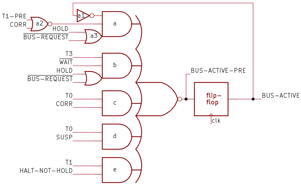
Next, I'll explain BUS-ACTIVE, an important signal that indicates if the bus is active or not. The Bus Interface Unit generates the BUS-ACTIVE signal to help control the state machine. The BUS-ACTIVE signal is also widely used in the Bus Interface Unit, controlling many functions such as transfers to and from the address registers. BUS-ACTIVE is generated by the complex circuit below that determines if the bus will be active, specifically in states T0 through T3. Because of the flip-flop, the computation of BUS-ACTIVE happens in the previous clock cycle.

The circuit to determine if the bus will be active next cycle.

The circuit to determine if the bus will be active next cycle.

In more detail, the signal BUS-ACTIVE-PRE indicates if the bus cycle will continue or will end on the next clock cycle. Delaying this signal through the flip-flop generates BUS-ACTIVE, which indicates if the bus is currently active in states T0 through T3. The top AND gate (a) is responsible for starting a cycle or keeping a cycle going (a1). It will allow a new cycle if there is a bus request (without HOLD) (a3). It will also allow a new cycle if there is a CORR micro-instruction prior to the T1 state (even if there is a HOLD, since this "fake" cycle won't use the bus) (a2). Finally, it allows a new cycle for a HALT, using T1-pre (a2).10 Next are the special cases that end a bus cycle. The second AND gate (b) ends the bus cycle after T3 unless there is a wait state or another bus request. (But a HOLD will block the next bus request.) The remaining gates end the cycle after T0 to preempt a prefetch if a CORR or SUSP micro-instruction occurs (d), or end after T1 for a HALT (e).

The BUS-ACTIVE circuit above uses a complex gate, a 5-input NOR gate fed by 5 AND gates with two attached OR gates. Surprisingly, this is implemented in the processor as a single gate with 14 inputs. Due to how gates are implemented with NMOS transistors, it is straightforward to implement this as a single gate. The inverter and NOR gate on the left, however, needed to be implemented separately, as they involve inversion; an NMOS gate must have a single inversion.

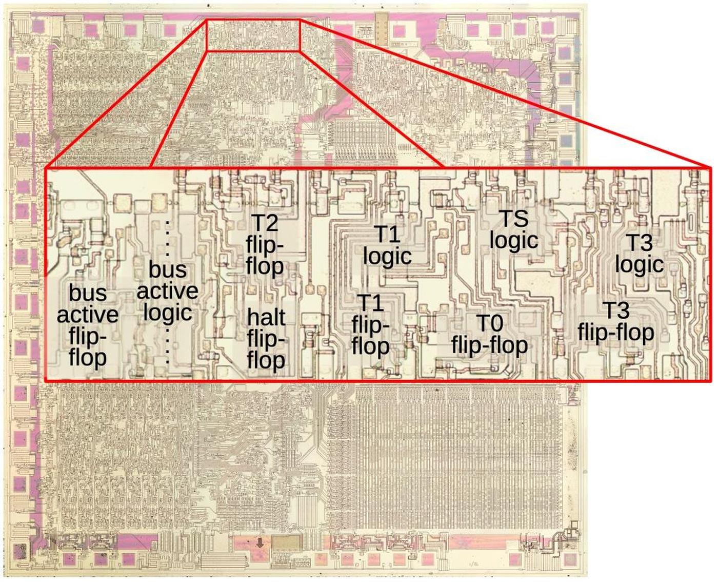
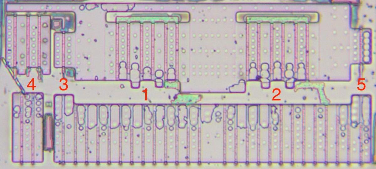
The bus state machine circuitry on the die.

The bus state machine circuitry on the die.

The diagram above shows the layout of the bus state machine circuitry on the die, zooming in on the top region of the die. The metal layer has been removed to expose the underlying silicon and polysilicon. The layout of each flip-flop is completely different, since the layout of each transistor is optimized to its surroundings. (This is in contrast to later processors such as the 386, which used standard-cell layout.) Even though the state machine consists of just a handful of flip-flops and gates, it takes a noticeable area on the die due to the large 3.2 µm feature size of the 8088. (Modern processors have features measured in nanometers, not micrometers.)

Conclusions

The bus state machine is an example of how the 8088's design consists of complications on top of complications. While the four-state bus cycle seems straightforward at first, it gets more complicated due to prefetching, wait states, the HALT instruction, and the bus hold feature, not to mention the interactions between these features. While there were good motivations behind these features, they made the processor considerably more complicated. Looking at the internals of the 8088 gives me a better understanding of why simple RISC processors became popular.

The bus state machine is a key part of the read and write circuitry, moving the bus operation through the necessary T-states. However, the state machine is not the only component in this process; a higher-level circuit decides when to perform a read, write, or prefetch, as well as breaking a 16-bit operation into two 8-bit operations.11 These circuits work together with the higher-level circuit telling the state machine when to go through the states.

In my next blog post, I'll describe the higher-level memory circuit so follow me on Twitter @kenshirriff or RSS for updates. I'm also on Mastodon as oldbytes.space@kenshirriff. If you're interested in the 8086, I wrote about the 8086 die, its die shrink process, and the 8086 registers earlier.

Notes and references

  1. The 8085 and 8088 processors both use a 4-step bus cycle for instruction fetching. For other reads and writes, the 8085's bus cycle has three steps compared to four for the 8088. Thus, the 8085 and 8088 bus cycles are similar but not an exact match. 

  2. The 8088 has separate instructions to read or write an I/O device. From the bus perspective, there's no difference between an I/O operation and a memory operation except that a pin on the chip indicates if the operation is for memory or I/O.

    The 8088 supports I/O operations for historical reasons, going back through the 8086, 8080, 8008, and the Datapoint 2200 system. In contrast, many other contemporary processors such as the 6502 used memory-mapped I/O, using standard memory accesses for I/O devices.

    The 8086 has a pin M/IO that is high for a memory access and low for an I/O access. External hardware uses this pin to determine how to handle the request. Confusingly, the pin's function is inverted on the 8088, providing IO/M. One motivation behind the 8088's 8-bit bus was to allow reuse of peripherals from the earlier 8-bit 8085 processor. Thus, the pin's function was inverted so it matched the 8085. (The pin is only available when the 8086/8088 is used in "minimum mode"; "maximum mode" remaps some of the pins, making the system more complicated but providing more control.) 

  3. I've made the timing diagram somewhat idealized so actions line up with the clock. In the real datasheet, all the signals are skewed by various amounts so the timing is more complicated. See the datasheet for pages of timing constraints on exactly when signals can change. 

  4. For more information on the implementation of the address adder, see my previous blog post

  5. The POP operation is an example of how the address adder updates a memory pointer. In this case, the stack address is moved from the Stack Pointer to the IND register in order to perform the memory read. As part of the read operation, the IND register is incremented by 2. The address is then moved from the IND register to the Stack Pointer. Thus, the address adder not only performs the segment arithmetic, but also computes the new value for the SP register.

    Note that the increment/decrement of the IND register happens after the memory operation. For stack operations, the SP must be decremented before a PUSH and incremented after a POP. The adder cannot perform a predecrement, so the PUSH instruction uses the ALU (Arithmetic/Logic Unit) to perform the decrement. 

  6. During the CORR micro-instruction, the Bus Interface Unit performs special TS and T0 states. Note that these states don't have any external effect, so they are invisible outside the processor. 

  7. The tradeoff with memory boards was that slower RAM chips were cheaper. The better RAM boards advertised "no wait states", but cheaper boards would add one or more wait states to every access, reducing performance. 

  8. Only the second half of the TS state has an effect on the Bus Interface Unit, so TS is not a full state like the other states. Specifically, a delayed TS signal is taken from the first half of the T0 flip-flop, and this signal is used to control various actions in the Bus Interface Unit. (Alternatively, you could think of this as an early T0 state.) This is why there isn't a separate flip-flop for the TS state. I suspect this is due to timing issues; by the time the TS state is generated by the logic, there isn't enough time to do anything with the state in that half clock cycle, due to propagation delays. 

  9. There is a bit more circuitry for the T1 state for a HALT. Specifically, there is a flip-flop that is set on this signal. On the next cycle, this flip-flop both blocks the generation of another T1 state and blocks the previous T1 state from progressing to T2. In other words, this flip-flop makes sure the special T1 lasts for one cycle. However, a HOLD state resets this flip-flop. That allows another special T1 to be generated when the HOLD ends. 

  10. The trickiest part of this circuit is using T1-pre to start a (short) cycle for HALT. The way it works is that the T1-pre signal only makes a difference if there isn't a bus cycle already active. The only way to get an "unexpected" T1-pre signal is if the state machine generates it for the first cycle of a HALT. Thus, the HALT triggers T1-pre and thus the bus-active signal. You might wonder why the bus-active uses this roundabout technique rather than getting triggered directly by HALT. The motivation is that the special T1 state for HALT requires the AND of three signals to ensure that the state is generated once for the HALT rather than continuously, but happens again after a HOLD, and waits until the current bus cycle is done. Instead of duplicating that AND gate, the circuit uses T1-pre which incorporates that logic. (This took me a long time to figure out.) 

  11. The 8088 has a 16-bit bus, compared to the 8088's 8-bit bus. Thus, a 16-bit bus operation on the 8088 will always require two 8-bit operations, while the 8086 can usually perform this operation in a single step. However, a 16-bit bus operation on the 8086 will still need to be broken into two 8-bit operations if the address is unaligned (i.e. odd). 

Reverse engineering the barrel shifter circuit on the Intel 386 processor die

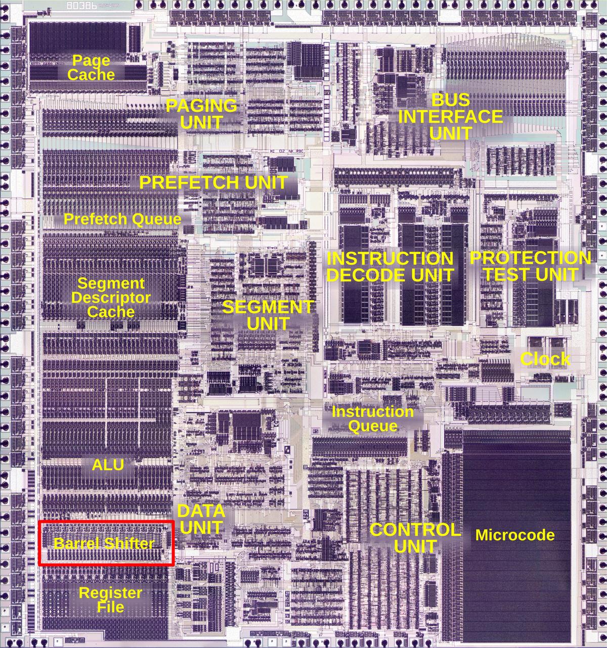
The Intel 386 processor (1985) was a large step from the 286 processor, moving x86 to a 32-bit architecture. The 386 also dramatically improved the performance of shift and rotate operations by adding a "barrel shifter", a circuit that can shift by multiple bits in one step. The die photo below shows the 386's barrel shifter, highlighted in the lower left and taking up a substantial part of the die.

The 386 die with the main functional blocks labeled. Click this image (or any other) for a larger version.)

The 386 die with the main functional blocks labeled. Click this image (or any other) for a larger version.)

Shifting is a useful operation for computers, moving a binary value left or right by one or more bits. Shift instructions can be used for multiplying or dividing by powers of two, and as part of more general multiplication or division. Shifting is also useful for extracting bit fields, aligning bitmap graphics, and many other tasks.1

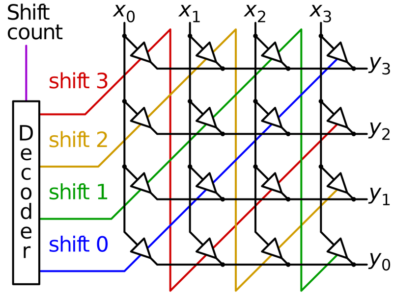
Barrel shifters require a significant amount of circuitry. A common approach is to use a crossbar, a matrix of switches that can connect any input to any output. By closing switches along a desired diagonal, the input bits are shifted. The diagram below illustrates a 4-bit crossbar barrel shifter with inputs X (vertical) and outputs Y (horizontal). At each point in the grid, a switch (triangle) connects a vertical input line to a horizontal output line. Energizing the blue control line, for instance, passes the value through unchanged (X0 to Y0 and so forth). Energizing the green control line rotates the value by one bit position (X0 to Y1 and so forth, with X3 wrapping around to X0). Similarly, the circuit can shift by 2 or 3 bits. The shift control lines select the amount of shift. These lines run diagonally, which will be important later.

A four-bit crossbar switch with inputs X and outputs Y. Image by Cmglee, CC BY-SA 3.0.

A four-bit crossbar switch with inputs X and outputs Y. Image by Cmglee, CC BY-SA 3.0.

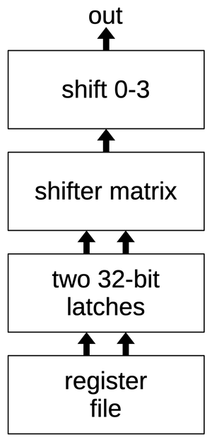
The main problem with a crossbar barrel shifter is that it takes a lot of hardware. The 386's barrel shifter has a 64-bit input and a 32-bit output,2 so the approach above would require 2048 switches (64×32). For this reason, the 386 uses a hybrid approach, as shown below. It has a 32×8 crossbar that can shift by 0 to 28 bits, but only in multiples of 4, making the circuit much smaller. The output from the crossbar goes to a second circuit that can shift by 0, 1, 2, or 3 bits. The combined circuitry supports an arbitrary shift, but requires less hardware than a complete crossbar. The inputs to the barrel shifter are two 32-bit values from the processor's register file, stored in latches for use by the shifter.

Block diagram of the barrel shifter circuit.

Block diagram of the barrel shifter circuit.

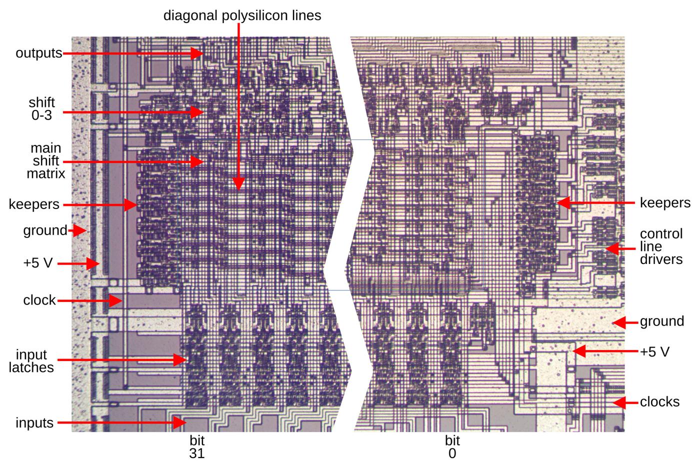
The figure below shows how the shifter circuitry appears on the die; this image shows the two metal layers on the die's surface. The inputs from the register file are at the bottom, for bits 31 through 0. Above that, the input latches hold the two 32-bit inputs for the shifter. In the middle is the heart of the shift circuit, the crossbar matrix. This takes the two 32-bit inputs and produces a 32-bit output. The matrix is controlled by sloping polysilicon lines, driven by control circuitry on the right. The matrix output goes to the circuit that applies a shift of 0 to 3 positions. Finally, the outputs exit at the top, where they go to other parts of the CPU. The shifter performs right shifts, but as will be explained below, the same circuit is used for the left shift instructions.

The barrel shifter circuitry as it appears on the die. I have cut out repetitive circuitry from the middle because the complete image is too wide to display clearly.

The barrel shifter circuitry as it appears on the die. I have cut out repetitive circuitry from the middle because the complete image is too wide to display clearly.

The barrel shifter crossbar matrix

In this section, I'll describe the matrix part of the barrel shifter circuit. The shift matrix takes 32-bit values a and b. Value b is shifted to the right, with bits from a filling in at the left, producing a 32-bit output. (As will be explained below, the output is actually 37 bits due to some complications, but ignore that for now.) The shift count is a multiple of 4 from 0 to 28.

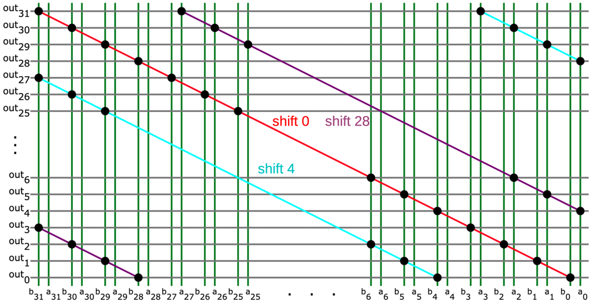
The diagram below illustrates the structure of the shift matrix. The two 32-bit inputs are provided at the bottom, interleaved, and run vertically. The 32 output lines run horizontally. The 8 control lines run diagonally, activating the switches (black dots) to connect inputs and outputs. (For simplicity, only 3 control lines are shown.) For a shift of 0, control line 0 (red) is selected and the output is b31b30...b1b0. (You can verify this by matching up inputs to outputs through the dots along the red line.)

Diagram of the shift matrix, showing three of the shift control lines.

Diagram of the shift matrix, showing three of the shift control lines.

For a shift right of 4, the cyan control line is activated. It can be seen that the output in this case is a3a2a1a0b31b30...b5b4, shifting b to the right 4 bits and filling in four bits from a as desired. For a shift of 28, the purple control line is activated, producing the output a27...a0b31...b28. Note that the control lines are spaced four bits apart, which is why the matrix only shifts by a multiple of 4. Another important feature is that below the red diagonal, the b inputs are connected to the output, while above the diagonal, the a inputs are connected to the output. (In other words, the black dots are shifted to the right above the diagonal.) This implements the 64-bit support, taking bits from a or b as appropriate.

Looking at the implementation on the die, the vertical wires use the lower metal layer (metal 1) while the horizontal wires use the upper metal layer (metal 2), so the wires don't intersect. NMOS transistors are used as the switches to connect inputs and outputs.4 The transistors are controlled by diagonal wires constructed of polysilicon that form the transistor gates. When a particular polysilicon wire is energized, it turns on the transistors along a diagonal line, connecting those inputs and outputs.

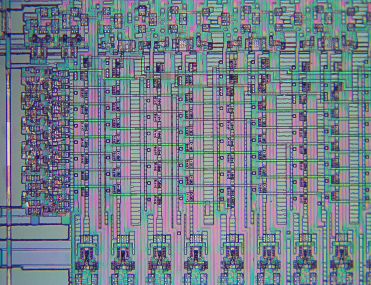
The image below shows the left side of the matrix.5 The polysilicon control lines are the green horizontal lines stepping down to the right. These control the transistors, which appear as columns of blue-gray squares next to the polysilicon lines. The metal layers have been removed; the position of the lower metal 1 layer is visible in the vertical bluish lines.

The left side of the matrix as it appears on the die.

The left side of the matrix as it appears on the die.

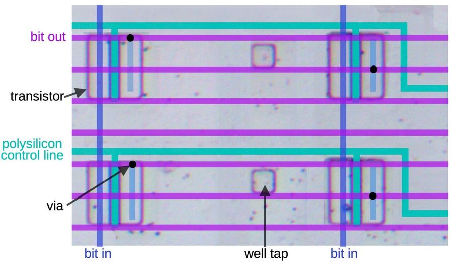
The diagram below shows four of these transistors in the shifter matrix. There are four circuitry layers involved. The underlying silicon is pinkish gray; the active regions are the squares with darker borders. Next is the polysilicon (green), which forms the control lines and the transistor gates. The lower metal layer (metal 1) forms the blue vertical lines that connect to the transistors.3 The upper metal layer (metal 2) forms the horizontal bit output lines. Finally, the small black dots are the vias that connect metal 1 and metal 2. (The well taps are silicon regions connected to ground to prevent latch-up.)

Four transistors in the shifter matrix. The polysilicon and metal lines have been drawn in.

Four transistors in the shifter matrix. The polysilicon and metal lines have been drawn in.

To see how this works, suppose the upper polysilicon line is activated, turning on the top two transistors. The two vertical bit-in lines (blue) will be connected through the transistors to the top two bit out lines (purple), by way of the short light blue metal segments and the via (black dot). However, if the lower polysilicon line is activated, the bottom two transistors will be turned on. This will connect the bit-in lines to the fifth and sixth bit-out lines, four lines down from the previous ones. Thus, successive polysilicon lines shift the connections down by four lines at a time, so the shifts change in steps of 4 bit positions.

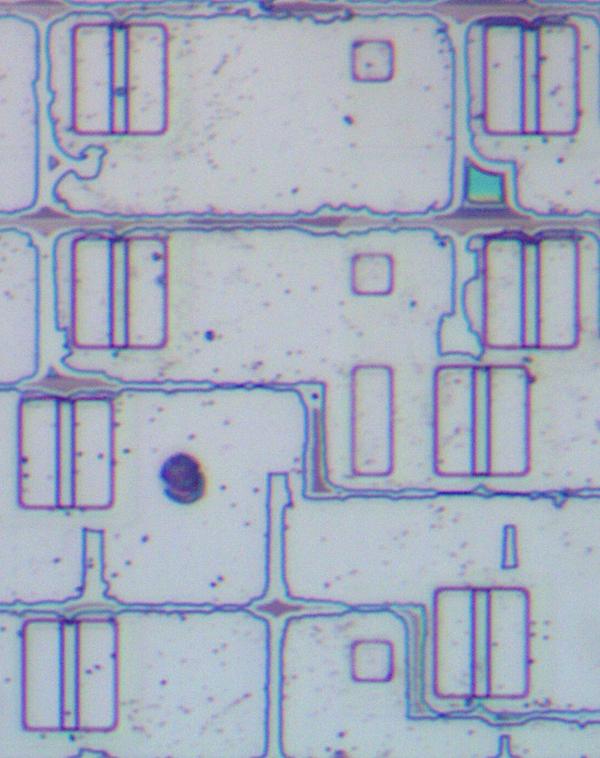
As mentioned earlier, to support the 64-bit input, the transistors below the diagonal are connected to b input while the transistors above the diagonal are connected to the a input. The photo below shows the physical implementation: the four upper transistors are shifted to the right by one wire width, so they connect to vertical a wires, while the four lower transistors are connected to b wires. (The metal wires were removed for this photo to show the transistors.)

This photo of the underlying silicon shows eight transistors. The top four transistors are shifted one position to the right. the irregular lines are remnants of other layers that I couldn't completely remove from the die.

This photo of the underlying silicon shows eight transistors. The top four transistors are shifted one position to the right. the irregular lines are remnants of other layers that I couldn't completely remove from the die.

In the matrix, the output signals run horizontally. In order for signals to exit the shifter from the top of the matrix, each horizontal output wire is connected to a vertical output wire. Meanwhile, other processor signals (such as the register write data) must also pass vertically through the shifter region. The result is a complicated layout, packing everything together as tightly as possible.

The precharge/keepers

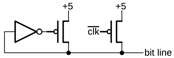
At the left and the right of the barrel shifter, repeated blocks of circuitry are visible. These blocks contain precharge and keeper circuits to hold the value on one of the lines. During the first clock phase, each horizontal bit line is precharged to +5 volts. Next, the matrix is activated and horizontal lines may be pulled low. If the line is not pulled low, the inverter and PMOS transistor will continuously pull the line high. The inverter and transistor can be viewed as a bus keeper, essentially a weak latch to hold the line in the 1 state. The keeper uses relatively weak transistors, so the line can be pulled low when the barrel shifter is activated. The purpose of the keeper is to ensure that the line doesn't drift into a state between 0 and 1. This is a bad situation with CMOS circuitry, since the pull-up and pull-down transistors could both turn on, yielding a short circuit.

The precharge/keeper circuit

The precharge/keeper circuit

The motivation behind this design is that implementing the matrix with "real" CMOS would require twice as many transistors. By implementing the matrix with NMOS transistors only, the size is reduced. In a standard NMOS implementation, pull-up transistors would continuously pull the lines high, but this results in fairly high power consumption. Instead, the precharge circuit pulls the line high at the start. But this results in dynamic logic, dependent on the capacitance of the circuit to hold the charge. To avoid the charge leaking away, the keeper circuit keeps the line high until it is pulled low. Thus, this circuit minimizes the area of the matrix as well as minimizing power consumption.

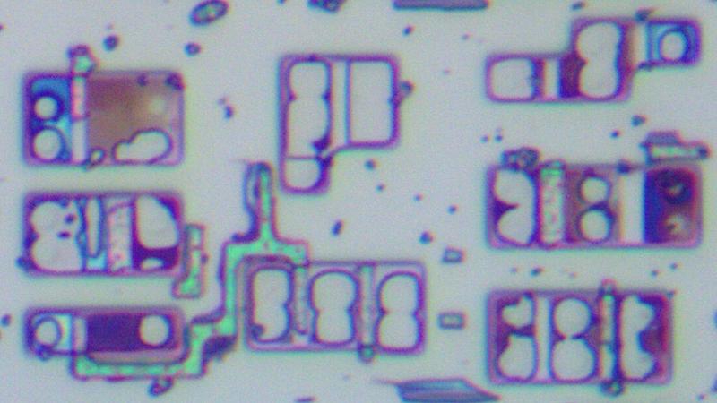
There are 37 keepers in total for the 37 output lines from the matrix.6 (The extra 5 lines will be explained below.) The photo below shows one block of three keepers; the metal has been removed to show the silicon transistors and some of the polysilicon (green).

One block of keeper circuitry, to the right of the shift matrix. This block has 12 transistors, supporting three bits.

One block of keeper circuitry, to the right of the shift matrix. This block has 12 transistors, supporting three bits.

The register latches

At the bottom of the shift circuit, two latches hold the two 32-bit input values. The 386 has multi-ported registers, so it can access two registers and write a third register at the same time. This allows the shift circuit to load both values at the same time. I believe that a value can also come from the 386's constant ROM, which is useful for providing 0, 1, or all-ones to the shifter.

The schematic below shows the register latches for one bit of the shifter. Starting at the bottom are the two inputs from the register file (one appears to be inverted for no good reason). Each input is stored in a latch, using the standard 386 latch circuit.7 The latched input is gated by the clock and then goes through multiplexers allowing either value to be used as either input to the shifter. (The shifter takes two 32-bit inputs and this multiplexer allows the inputs to be swapped to the other sides of the shifter.) A second latch stage holds the values for the output; this latch is cleared during the first clock phase and holds the desired value during the second clock phase.

Circuit for one bit of the register latch.

Circuit for one bit of the register latch.

The die photo below shows the register latch circuit, contrasting the metal layers (left) with the silicon layer (right). The dark spots in the metal image are vias between the metal layers or connections to the underlying silicon or polysilicon. The metal layer is very dense with vertical wiring in the lower metal 1 layer and horizontal wiring in the upper metal 2 layer. The density of the chip seems to be constrained by the metal wiring more than the density of the transistors.

One of the register latch circuits.

One of the register latch circuits.

The 0-3 shifter

The shift matrix can only shift in steps of 4 bits. To support other shifts, a circuit at the top of the shifter provides a shift of 0 to 3 bits. In conjunction, these circuits permit a shift by an arbitrary amount.8 The schematic below shows the circuit. A bit enters at the bottom. The first shift stage passes the bit through, or sends it one bit position to the right. The second stage passes the bit through, or sends it two bit positions to the right. Thus, depending on the control lines, each bit can be shifted by 0 to 3 positions to the right. At the top, a transistor pulls the circuit low to initialize it; the NOR gate at the bottom does the same. A keeper transistor holds the circuit low until a data bit pulls it high.

One bit of the 0-3 shifter circuit.

One bit of the 0-3 shifter circuit.

The diagram below shows the silicon implementation corresponding to two copies of the schematic above. The shifters are implemented in pairs to slightly optimize the layout. In particular, the two NOR gates are mirrored so the power connection can be shared. This is a small optimization, but it illustrates that the 386 designers put a lot of work into making the layout dense.

Two bits of the 0-3 shifter circuit as it appears on the die.

Two bits of the 0-3 shifter circuit as it appears on the die.

Complications

As is usually the case with x86, there are a few complications. One complication is that the shift matrix has 37 outputs, rather than the expected 32. There are two reasons behind this. First, the upper shifter will shift right by up to 3 positions, so it needs 3 extra bits. Thus, the matrix needs to output bits 0 through 34 so three bits can be discarded. Second, shift instructions usually produce a carry bit from the last bit shifted out of the word. To support this, the shift matrix provides an extra bit at both ends for use as the carry. The result is that the matrix produces 37 outputs, which can be viewed as bits -1 through 35.

Another complication is that the x86 instruction set supports shifts on bytes and 16-bit words as well as 32-bit words. If you put two 8-bit bytes into the shifter, there will be 24 unused bits in between, posing a problem for the shifter. The solution is that some of the diagonal control lines in the matrix are split on byte and word boundaries, allowing an 8- or 16-bit value to be shifted independently. For example, you can perform a 4-bit right shift on the right-hand byte, and a 28-bit right shift on the left-hand byte. This brings the two bytes together in the result, yielding the desired 4-bit right shift. As a result, there are 18 diagonal control lines in the shifter (if I counted correctly), rather than the expected 8 control lines. This makes the circuitry to drive the control lines more complicated, as it must generate different signals depending on the size of the operand.

The control circuitry

The control circuitry at the right of the shifter drives the diagonal polysilicon lines in the matrix, selecting the desired shift. It also generates control signals for the 0-3 shifter, selecting a shift-by-1 or shift-by-2 as necessary. This circuitry operates under the control of the microcode, which tells it when to shift. It gets the shift amount from the instruction or the CL register and generates the appropriate control signals.

The distribution of control signals is more complex than you might expect. If possible, the polysilicon diagonals are connected on the right of the matrix to the control circuitry, providing a direct connection. However, many of the diagonals do not extend all the way to the right, either because they start on the left or because they are segmented for 8- or 16-bit values. Some of these signals are transmitted through polysilicon lines that run underneath the matrix. Others are transmitted through horizontal metal lines that run through the register latches. (These latches don't use many horizontal lines, so there is available space to route other signals.) These signals then ascend through the matrix at various points to connect with the polysilicon lines. This shows that the routing of this circuitry is carefully optimized to make it as compact as possible. Moreover, these "extra" lines disrupt the layout; the matrix is almost a regular pattern, but it has small irregularities throughout.

Implementing x86 shifts and rotates with the barrel shifter

The x86 has a variety of shift and rotate instructions.9 It is interesting to consider how they are implemented using the barrel shifter, since it is not always obvious. In this section, I'll discuss the instructions supported by the 386.

One important principle is that even though the circuitry shifts to the right, by changing the inputs this can achieve a shift to the left. To make this concrete, consider two input words a and b, with the shifter extracting the portion in red below. (I'll use 8-bit examples instead of 32-bit here and below to keep the size manageable.) The circuit shifts b to the right five bits, inserting bits from a at the left. Alternatively, the result can be viewed as shifting a to the left three bits, inserting bits from b at the right. Thus, the same result can be viewed as a right shift of b or a left shift of a. This holds in general, with a 32-bit right shift by N bits equivalent to a left shift by 32-N bits, depending on which word10 you focus on.

a7a6a5a4a3a2a1a0b7b6b5b4b3b2b1b0

Double shifts

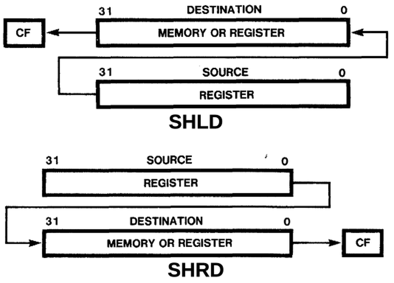
The double-shift instructions (Shift Left Double (SHLD) and Shift Right Double (SHRD)) were new in the 386, shifting two 32-bit values to produce a 32-bit result. The last bit shifted out goes into the carry flag (CF). These instructions map directly onto the behavior of the barrel shifter, so I'll start with them.

Actions of the double shift instructions.

Actions of the double shift instructions.

The examples below show how the shifter implements the SHLD and SHRD instructions; the shifter output is highlighted in red. (These examples use an 8-bit source (s) and destination (d) to keep them manageable.) In either case, 3 bits of the source are shifted into the destination; shifting left or right is just a matter of whether the destination is on the left or right.

SHLD 3: ddddddddssssssss

SHRD 3: ssssssssdddddddd

Shifts

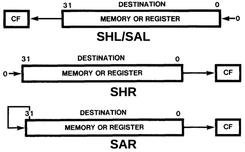
The basic shift instructions are probably the simplest. Shift Arithmetic Left (SAL) and Shift Logical Left (SHL) are synonyms, shifting the destination to the left and filling with zeroes. This can be accomplished by performing a shift with the word on the left and zeroes on the right. Shift Logical Right (SHR) is the opposite, shifting to the right and filling with zeros. This can be accomplished by putting the word on the right and zeroes on the left. Shift Arithmetic Right (SAR) is a bit different. It fills with the sign bit, the top bit. The purpose of this is to shift a signed number while preserving its sign. It can be implemented by putting all zeroes or all ones on the left, depending on the sign bit. Thus, the shift instructions map nicely onto the barrel shifter.

Actions of the shift instructions.

Actions of the shift instructions.

The 8-bit examples below show how the shifter accomplishes the SHL, SHR, and SAR instructions. The destination value d is loaded into one half of the shifter. For SAR, the value's sign bit s is loaded into the other half of the shifter, while the other instructions load 0 into the other half of the shifter. The red box shows the output from the shifter, selected from the input.

SHL 3: dddddddd00000000

SHR 3: 00000000dddddddd

SAR 3: ssssssssdddddddd

Rotates

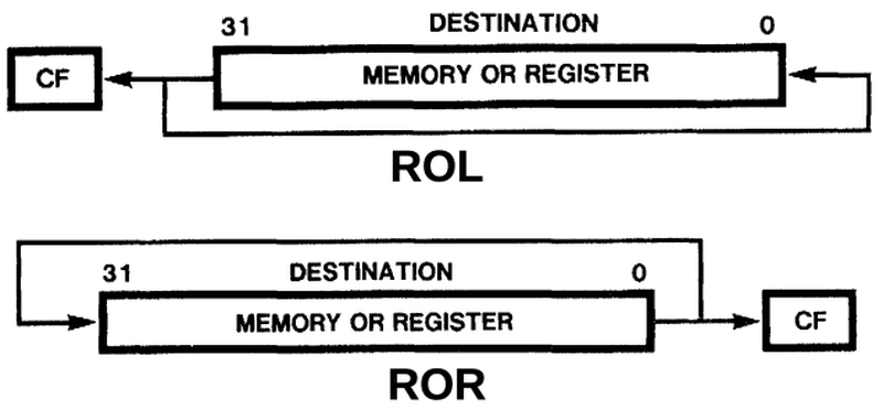
Unlike the shift instructions, the rotate instructions preserve all the bits. As bits shift off one end, they fill in the other end, so the bit sequence rotates. A rotate left or right is implemented by putting the same word on the left and right.

Actions of the rotate instructions.

Actions of the rotate instructions.

The shifter implements rotates as shown below, using the destination value as both shifter inputs. A left shift by N bits is implemented by shifting right by 32-N bits.

ROL 3: d7d6d5d4d3d2d1d0d7d6d5d4d3d2d1d0

ROR 3: d7d6d5d4d3d2d1d0d7d6d5d4d3d2d1d0

Rotates through carry

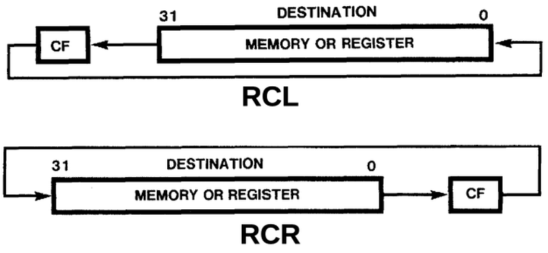
The rotate through carry instructions perform 33-bit rotates, rotating the value through the carry bit. You might wonder how the barrel shifter can perform a 33-bit rotate, and the answer is that it can't. Instead, the instruction takes multiple steps. If you look at the instruction timings, the other shifts and rotates take three clock cycles. Rotating through the carry, however, takes nine clock cycles, performing multiple steps under the control of the microcode.

Actions of the rotate through carry instructions.

Actions of the rotate through carry instructions.

Without looking at the microcode, I can only speculate how it takes place. One sequence would be to get the top bits by putting zeroes in the right 32 bits and shifting. Next, get the bottom bits by putting the carry bit in the left 32 bits and shifting one bit more. (That is, set the left 32-bit input to either the constant 0 or 1, depending on the carry.) Finally, the result can be generated by ORing the two shift values together. The example below shows how an RCL 3 could be implemented. In the second step, the carry value C is loaded into the left side of the shifter, so it can get into the result. Note that bit d5 ends up in the carry bit, rather than the result. The RCR instruction would be similar, but adjusting the shift parameters accordingly.

First shift: d7d6d5d4d3d2d1d000000000

Second shift: 0000000Cd7d6d5d4d3d2d1d0

Result from OR: d4d3d2d1d0Cd7d6

Conclusions

The shifter circuit illustrates how the rapidly increasing transistor counts in the 1980s allowed new features. Programming languages make it easy to shift numbers with an expression such as a>>5. But it takes a lot of hardware in the processor to perform these shifts efficiently. The additional hardware of the 386's barrel shifter dramaticallly improved shift performance for shifts and rotates compared to earlier x86 processors. I estimate that the barrel shifter requires about 2000 transistors, about half the number of the entire 6502 processor (1975). But by 1985, putting 2000 transistors into a feature was practical. (In total, the 386 contains 285,000 transistors, a trivial number now, but a large number for the time.)

I plan to write more about the 386, so follow me on Twitter @kenshirriff or RSS for updates. I'm also on Mastodon occasionally as @[email protected].

Notes and references

  1. The earliest reference for a barrel shifter is often given as "A barrel switch design", Computer Design, 1972, but the idea of a barrel shifter goes back to 1964 at least. (The "barrel switch" name presumably comes from a physical barrel switch, a cylindrical multi-position switch such as a car ignition.) The CDC 6600 supercomputer (1964) had a 6-stage shifter able to shift up to 63 positions in one cycle (details); it was called a "parallel shifting network" rather than a "barrel shifter". A Burroughs patent filed in 1965 describes a barrel switch "capable of performing logical switching operations in a single time involving any amount of binary information," so the technology is older.

    Early microprocessors shifted by one bit position at a time. Although the Intel 8086 provided instructions to shift by multiple bits at a time, this was implemented internally by a microcode loop, so the more bits you shifted, the longer the instruction took, four clock cycles per bit. Shifting on the 286 was faster, taking one additional cycle for each bit position shifted. The first ARM processor (ARM1, 1985) included a 32-bit barrel shifter. It was considerably simpler than the 386's design, following ARM's RISC philosophy. 

  2. The 386 Hardware Reference Manual states that the 386 contains a 64-bit barrel shifter. I find this description a bit inaccurate, since the output is only 32 bits, so the barrel shifter is much simpler than a full 64-bit barrel shifter. 

  3. The 386 has two layers of metal. The vertical lines are in the lower layer of metal (metal 1) while the horizontal lines are in the upper layer of metal (metal 2). Transistors can only connect to lower metal, so the connection between the horizontal line and the transistor uses a short piece of lower metal to bridge the layers. 

  4. Each row of the matrix can be considered a multiplexer with 8 inputs, implemented by 8 pass transistors. One of the eight transistors is activated, passing that input to the output. 

  5. The image below shows the full shift matrix. Click the image for a much larger view.

    The matrix with the metal layer removed.

    The matrix with the metal layer removed.


  6. The keepers are arranged with 6 blocks of three on the left and 6 blocks of 3 on the right, plus an additional one at the bottom right. 

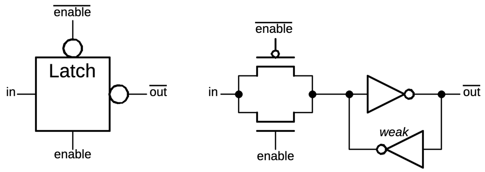
  7. The standard latch in the 386 consists of two cross-coupled inverters forming a static circuit to hold a bit. The input goes through a transmission gate (back-to-back NMOS and PMOS transistors) to the inverters. One inverter is weak, so it can be overpowered by the input. The 8086, in contrast, uses dynamic latches that depend on the gate capacitance to hold a bit. 

  8. Some shifters take the idea of combining shift circuits to the extreme. If you combine a shift-by-one circuit, a shift-by-two circuit, a shift-by-four circuit, and so forth, you end up with a logarithmic shifter: selecting the appropriate stages provide an arbitrary shift. (This design was used in the CDC 6600.) This design has the advantage of reducing the amount of circuitry since it uses log2(N) layers rather than N layers. However, the logarithmic approach has performance disadvantages since the signals need to go through more circuitry. This paper describes various design alternatives for barrel shifters. 

  9. The basic rotate left and right instructions date back to the Datapoint 2200, the ancestor of the 8086 and x86. The rotate left through carry and rotate right through carry instructions in x86 were added in the Intel 8008 processor and the 8080 was the same. The MOS 6502 had a different set of rotates and shifts: arithmetic shift left, rotate left, logical shift right, and rotate right; the rotate instructions rotated through the carry. The Z-80 had a more extensive set: rotates left and right, either through the carry or not, shift left, shift right logical, shift right arithmetic, and 4-bit digit rotates left and right through two bytes. The 8086's set of rotates and shifts was similar to the Z-80, except it didn't have the digit rotates. The 8086 also supported shifting and rotating by multiple positions. This illustrates that there isn't a "natural" set of shift and rotate instructions. Instead, different processors supported different instructions, with complexity generally increasing over time. 

  10. The x86 uses "word" to refer to a 16-bit value and "double word" or "dword" to refer to a 32-bit value. I'm going to ignore the word/dword distinction. 

Inside the Intel 386 processor die: the clock circuit

Processors are driven by a clock, which controls the timing of each step inside the chip. In this blog post, I'll examine the clock-generation circuitry inside the Intel 386 processor. Earlier processors such as the 8086 (1978) were simpler, using two clock phases internally. The Intel 386 processor (1985) was a pivotal development for Intel as it moved x86 to CMOS (as well as being the first 32-bit x86 processor). The 386's CMOS circuitry required four clock signals. An external crystal oscillator provided the 386 with a single clock signal and the 386's internal circuitry generated four carefully-timed internal clock signals from the external clock.

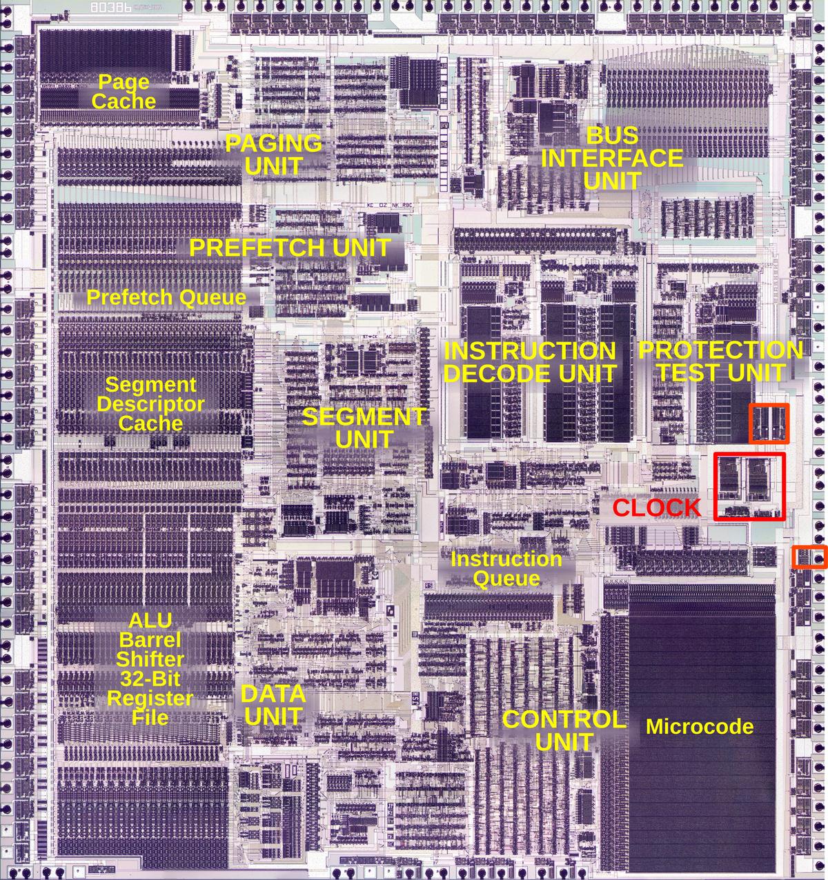
The die photo below shows the Intel 386 processor with the clock generation circuitry and clock pad highlighted in red. The heart of a processor is the datapath, the components that hold and process data. In the 386, these components are in the lower left: the ALU (Arithmetic/Logic Unit), a barrel shifter to shift data, and the registers. These components form regular rectangular blocks, 32 bits wide. In the lower right is the microcode ROM, which breaks down machine instructions into micro-instructions, the low-level steps of the instruction. Other parts of the chip prefetch and decode instructions, and handle memory paging and segmentation. All these parts of the chip run under the control of the clock signals.

The 386 with the main functional blocks labeled. Click this image (or any other) for a larger version.

The 386 with the main functional blocks labeled. Click this image (or any other) for a larger version.

A brief discussion of clock phases

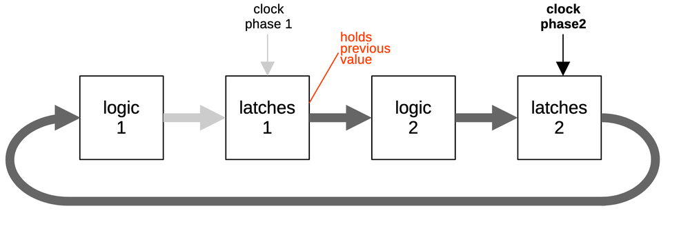
Many processors use a two-phase clock to control the timing of the internal processing steps. The idea is that the two clock phases alternate: first phase 1 is high, and then phase 2 is high, as shown below. During each clock phase, logic circuitry processes data. A circuit called a "transparent latch" is used to hold data between steps.2 The concept of a latch is that when a latch's clock input is high, the input passes through the latch. But when the latch's clock input is low, the latch remembers its previous value. With two clock phases, alternating latches are active one at a time, so data passes through the circuit step by step, under the control of the clock.

The two-phase clock signal used by the Intel 8080 processor. The 8080 uses asymmetrical clock signals, with phase 2 longer than phase 1. From the 8080 datasheet.

The two-phase clock signal used by the Intel 8080 processor. The 8080 uses asymmetrical clock signals, with phase 2 longer than phase 1. From the 8080 datasheet.

The diagram below shows an abstracted model of the processor circuitry. The combinational logic (i.e. the gate logic) is divided into two blocks, with latches between each block. During clock phase 1, the first block of latches passes its input through to the output. Thus, values pass through the first logic block, the first block of latches, and the second logic block, and then wait.

Action during clock phase 1.

Action during clock phase 1.

During clock phase 2 (below), the first block of latches stops passing data through and holds the previous values. Meanwhile, the second block of latches passes its data through. Thus, the first logic block receives new values and performs logic operations on them. When the clock switches to phase 1, processing continues as in the first diagram. The point of this is that processing takes place under the control of the clock, with values passed step-by-step between the two logic blocks.1

Action during clock phase 2.

Action during clock phase 2.

This circuitry puts some requirements on the clock timing. First, the clock phases must not overlap. If both clocks are active at the same time, data will flow out of control around the loop, messing up the results.3 Moreover, because the two clock phases probably don't arrive at the exact same time (due to differences in the wiring paths), a "dead zone" is needed between the two phases, an interval where both clocks are low, to ensure that the clocks don't overlap even if there are timing skews. Finally, the clock frequency must be slow enough that the logic has time to compute its result before the clock switches.

Many processors such as the 8080, 6502, and 8086 used this type of two-phase clocking. Early processors such as the 8008 (1972) and 8080 (1974) required complicated external circuitry to produce two asymmetrical clock phases.4 For the 8080, Intel produced a special clock generator chip (the 8224) that produced the two clock signals according to the required timing. The Motorola 6800 (1974) required two non-overlapping (but at least symmetrical) clocks, produced by the MC6875 clock generator chip. The MOS 6502 processor (1975) simplified clock generation by producing the two phases internally (details) from a single clock input. This approach was used by most later processors.

An important factor is that the Intel 386 processor was implemented with CMOS circuitry, rather than the NMOS transistors of many earlier processors. A CMOS chip uses both NMOS transistors (which turn on when the gate is high) and PMOS transistors (which turn on when the gate is low).7 Thus, the 386 requires an active-high clock signal and an active-low clock signal for each phase,5 four clock signals in total.6 In the rest of this article, I'll explain how the 386 generates these four clock signals.

The clock circuitry

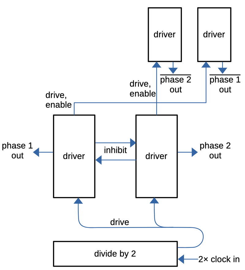
The block diagram below shows the components of the clock generation circuitry. Starting at the bottom, the input clock signal (CLK2, at twice the desired frequency) is divided by two to generate two drive signals with opposite phases. These signals go to the large driver circuits in the middle, which generate the two main clock signals (phase 1 and phase 2). Each driver sends an "inhibit" signal to the other when active, ensuring that the phases don't overlap. Each driver also sends signals to a smaller driver that generates the inverted clock signal. The "enable" signal shapes the output to prevent overlap. The four clock output signals are then distributed to all parts of the processor.

Block diagram of the clock circuitry. The layout of the blocks matches their approximate physical arrangement.

Block diagram of the clock circuitry. The layout of the blocks matches their approximate physical arrangement.

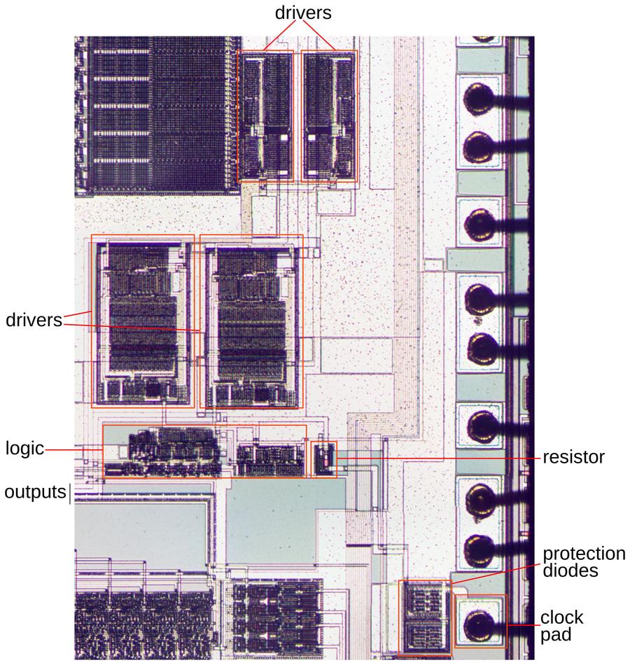
The diagram below shows a closeup of the clock circuitry on the die. The external clock signal enters the die at the clock pad in the lower right. The signal is clamped by protection diodes and a resistor before passing to the divide-by-two logic, which generates the two clock phases. The four driver blocks generate the high-current clock pulses that are transmitted to the rest of the chip by the four output lines at the left.

Details of the clock circuitry. This image shows the two metal layers. At the right, bond wires are connected to the pads on the die.

Details of the clock circuitry. This image shows the two metal layers. At the right, bond wires are connected to the pads on the die.

Input protection

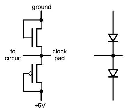
The 386 has a pin "CLK2" that receives the external clock signal. It is called CLK2 because this signal has twice the frequency of the 386's clock. The chip package connects the CLK2 pin through a tiny bond wire (visible above) to the CLK2 pad on the silicon die. The CLK2 input has two protection diodes, created from MOSFETs, as shown in the schematic below. If the input goes below ground or above +5 volts, the corresponding diode will turn on and clamp the excess voltage, protecting the chip. The schematic below shows how the diodes are constructed from an NMOS transistor and a PMOS transistor. The schematic corresponds to the physical layout of the circuit, so power is at the bottom and the ground is at the top.

The input protection circuit. The left shows the physical circuit built from an NMOS transistor and a PMOS transistor, while the right shows the equivalent diode circuit.

The input protection circuit. The left shows the physical circuit built from an NMOS transistor and a PMOS transistor, while the right shows the equivalent diode circuit.

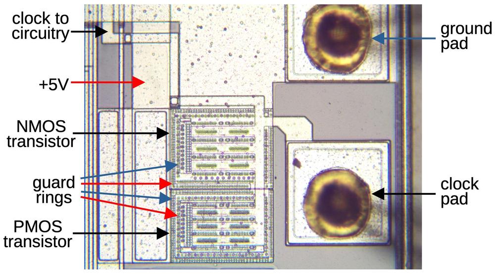
The diagram below shows the implementation of these protection diodes (i.e. transistors) on the die. Each transistor is much larger than the typical transistors inside the 386, because these transistors must be able to handle high currents. Physically, each transistor consists of 12 smaller (but still relatively large) transistors in parallel, creating the stripes visible in the image. Each transistor block is surrounded by two guard rings, which I will explain in the next section.

This diagram shows the circuitry next to the clock pad.

This diagram shows the circuitry next to the clock pad.

Latch-up and the guard rings

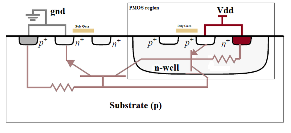
The phenomenon of "latch-up" is the hobgoblin of CMOS circuitry, able to destroy a chip. Regions of the silicon die are doped with impurities to form N-type and P-type silicon. The problem is that the N- and P-doped regions in a CMOS chip can act as parasitic NPN and PNP transistors. In some circumstances, these transistors can turn on, shorting power and ground. Inconveniently, the transistors latch into this state until the power is removed or the chip burns up. The diagram below shows how the substrate, well, and source/drain regions can combine to act as unwanted transistors.8

This diagram illustrates how the parasitic NPN and PNP transistors are formed in a CMOS chip. Note that the 386's construction is opposite from this diagram, with an N substrate and P well. Image by Deepon, CC BY-SA 3.0.

This diagram illustrates how the parasitic NPN and PNP transistors are formed in a CMOS chip. Note that the 386's construction is opposite from this diagram, with an N substrate and P well. Image by Deepon, CC BY-SA 3.0.

Normally, P-doped substrate or wells are connected to ground and the N-doped substrate or wells are connected to +5 volts. As a result, the regions act as reverse-biased diodes and no current flows through the substrate. However, a voltage fluctuation or large current can disturb the reverse biasing and the resulting current flow will turn on these parasitic transistors. Unfortunately, these parasitic transistors drive each other in a feedback loop, so once they get started, they will conduct more and more strongly and won't stop until the chip is powered down. The risk of latch-up is highest with circuits connected to the unpredictable voltages of the outside world, or high-current circuits that can cause power fluctuations. The clock circuitry has both of these risks.

One way of protecting against latch-up is to put a guard ring around a potentially risky circuit. This guard ring will conduct away the undesired substrate current before it can cause latch-up. In the case of the 386, two concentric guard rings are used for additional protection.9 In the earlier die photo, these guard rings can be seen surrounding the transistors. Guard rings will also play a part in the circuitry discussed below.

Polysilicon resistor

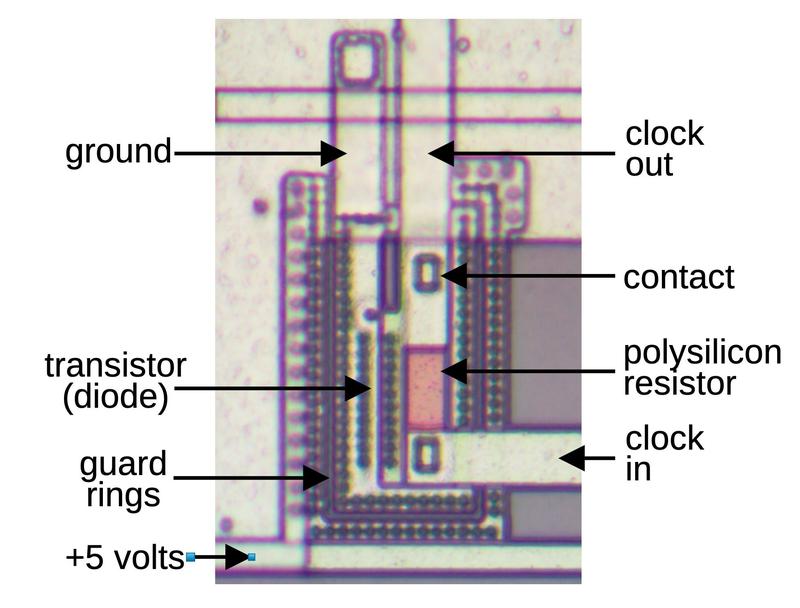
After the protection diodes, the clock signal passes through a polysilicon resistor, followed by another protection diode. Polysilicon is a special form of silicon that is used for wiring and also forms the transistor gates. The polysilicon layer sits on top of the base silicon; polysilicon has a moderate amount of resistance, considerably more than metal, so it can be used as a resistor.

The image below shows the polysilicon resistor along with a protection diode. This circuit provides additional protection against transients in the clock signal.10 This circuit is surrounded by two concentric guard rings for more latch-up protection.

The polysilicon resistor and associated diode.

The polysilicon resistor and associated diode.

The divide-by-two logic

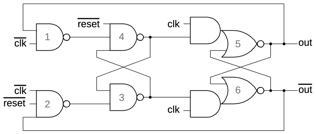
The input clock to the 386 runs at twice the frequency of the internal clock. The circuit below divides the input clock by 2, producing complemented outputs. This circuit consists of two set-reset latch stages, one driven by the input clock inverted and the second driven by the input clock, so the circuit will update once per input clock cycle. Since there are three inversions in the loop, the output will be inverted for each update, so it will cycle at half the rate of the input clock. The reset input is asymmetrical: when it is low, it will force the output low and the complemented output high. Presumably, this ensures that the processor starts with the correct clock phase when exiting the reset state.

The divide-by-two circuit.

The divide-by-two circuit.

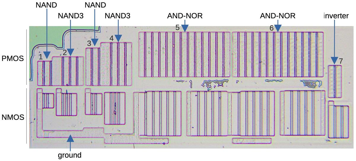
I have numbered the gates above to match their physical locations below. In this image, I have etched the chip down to the silicon so you can see the active silicon regions. Each logic gate consists of PMOS transistors in the upper half and NMOS transistors in the lower half. The thin stripes are the transistor gates; the two-input NAND gates have two PMOS transistors and two NMOS transistors, while the three-input NAND gates have three of each transistor. The AND-NOR gates need to drive other circuits, so they use paralleled transistors and are much larger. Each AND-NOR gate contains 12 PMOS transistors, four for each input, but uses only 9 NMOS transistors. Finally, the inverter (7) inverts the input clock signal for this circuit. The transistors in each gate are sized to maximize performance and minimize power consumption. The two outputs from the divider then go through large inverters (not shown) that feed the driver circuits.11

The silicon for the divide-by-two circuit as it appears on the die.

The silicon for the divide-by-two circuit as it appears on the die.

The drivers

Because the clock signals must be transmitted to all parts of the die, large transistors are required to generate the high-current pulses. These large transistors, in turn, are driven by medium-sized transistors. Additional driver circuitry ensures that the clock signals do not overlap. There are four driver circuits in total. The two larger, lower driver circuits generate the positive clock pulses. These drivers control the two smaller, upper driver circuits that generate the inverted clock pulses.

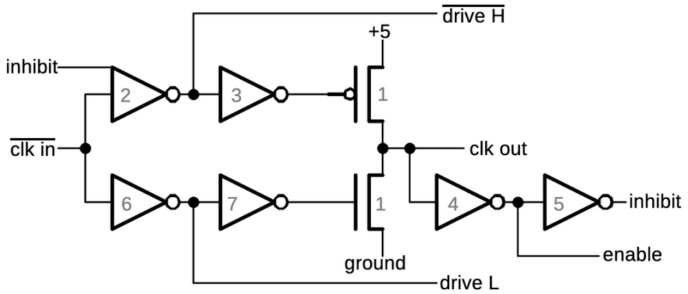
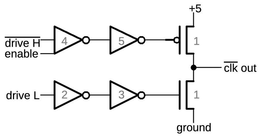
First, I'll discuss the larger, positive driver circuit. The core of the driver consists of the large PMOS transistor (1) to pull the output high, and the large NMOS transistor (1) to pull the output low. Each transistor is driven by two inverters (2/3 and 6/7 respectively). The circuit also produces two signals to shape the outputs from the other drivers. When the clock output is high, the "inhibit" signal goes to the other lower driver and inhibits that driver from pulling its output high.12 This prevents overlap in the output between the two drivers. When the clock output is low, an "enable" output goes to the inverted driver (discussed below) to enable its output. The transistor sizes and propagation delays in this circuit are carefully designed to shape the internal clock pulses as needed.

Schematic of the lower driver.

Schematic of the lower driver.

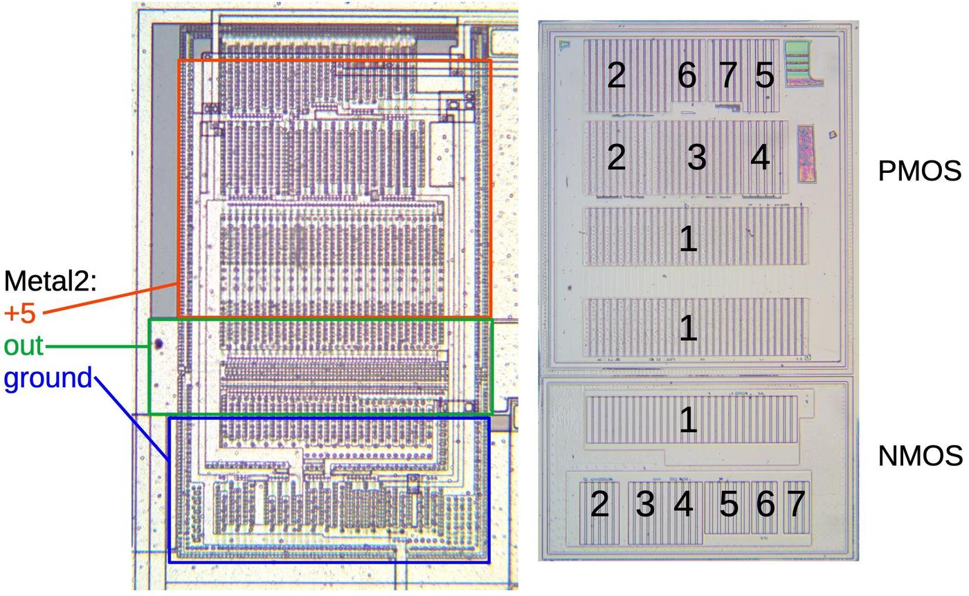
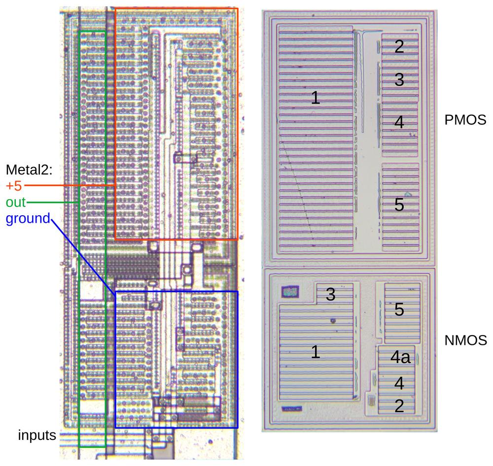
The diagram below shows how this driver is implemented on the die. The left image shows the two metal layers. The right image shows the transistors on the underlying silicon. The upper section holds PMOS transistors, while the lower section holds NMOS transistors. Because PMOS transistors have poorer performance than NMOS transistors, they need to be larger, so the PMOS section is larger. The transistors are numbered, corresponding to the schematic above. Each transistor is physically constructed from multiple transistors in parallel. The two guard rings are visible in the silicon, surrounding and separating the PMOS and NMOS regions.

One of the lower drivers. The left image shows metal while the right image shows silicon.

One of the lower drivers. The left image shows metal while the right image shows silicon.

The 386 has two layers of metal wiring. In this circuit, the top metal layer (M2) provides +5 for the PMOS transistors, ground for the NMOS transistors, and receives the output, all through large rectangular regions. The lower metal layer (M1) provides the physical source and drain connections to the transistors as well as the wiring between the transistors. The pattern of the lower metal layer is visible in the left photo. The dark circles are connections between the lower metal layer and the transistors or the upper metal layer. The connections to the two guard rings are visible around the edges.

Next, I'll discuss the two upper drivers that provided the inverted clock signals. These drivers are smaller, presumably because less circuitry needs the inverted clocks. Each upper driver is controlled by enable and drive from the corresponding lower driver. As before, two large transistors pull the output high or low, and are driven by inverters. The enable input must be high for inverter 4 to go low Curiously, the enable input is wired to the output of inverter 4. Presumably, this provides a bit of shaping to the signal.

Schematic of the upper driver.

Schematic of the upper driver.

The layout (below) is roughly similar to the previous driver, but smaller. The driver transistors (1) are arranged vertically rather than horizontally, so the metal 2 rectangle to get the output is on the left side rather than in the middle. The transistor wiring is visible in the lower (metal 1) layer, running vertically through the circuit. As before, two guard rings surround the PMOS and NMOS regions.

One of the upper drivers. The left image shows metal while the right image shows silicon.

One of the upper drivers. The left image shows metal while the right image shows silicon.

Distribution

Once the four clock signals have been generated, they are distributed to all parts of the chip. The 386 has two metal layers. The top metal layer (M2) is thicker, so it has lower resistance and is used for clock (and power) distribution where possible. The clock signal will use the lower M1 metal layer when necessary to cross other M2 signals, as well as for branch lines off the main clock lines.

The diagram below shows part of the clock distribution network; the four parallel clock lines are visible similarly throughout the chip. The clock signal arrives at the upper right and travels to the datapath circuitry on the left. As you can see, the four clock lines are much wider than the thin signal lines; this width reduces the resistance of the wiring, which reduces the RC (resistive-capacitive) delay of the signals. The outlined squares at each branch are the vias, connections between the two metal layers. At the right, the incoming clock signals are in layer M1 and zig-zag to cross under other signals in M2. The clock distribution scheme in the 386 is much simpler than in modern processors.

Part of the wiring for clock distribution. This image spans about 1/5 of the chip's width.

Part of the wiring for clock distribution. This image spans about 1/5 of the chip's width.

Clocks in modern processors

The 386's internal clock speed was simply the external clock divided by 2. However, modern processors allow the clock speed to be adjusted to optimize performance or to overclock the chip. This is implemented by an on-chip PLL (Phase-Locked Loop) that generates the internal clock from a fixed external clock, multiplying the clock speed by a selectable multiplier. Intel introduced a PLL to the 80486 processor, but the multipler was fixed until the Pentium.

The Intel 386's clock can go up to 40 megahertz. Although this was fast for the time, modern processors are over two orders of magnitude faster, so keeping the clock synchronized in a modern processor requires complex techniques.13 With fast clocks, even the speed of light becomes a constraint; at 6 GHz, light can travel just 5 centimeters during a clock cycle.

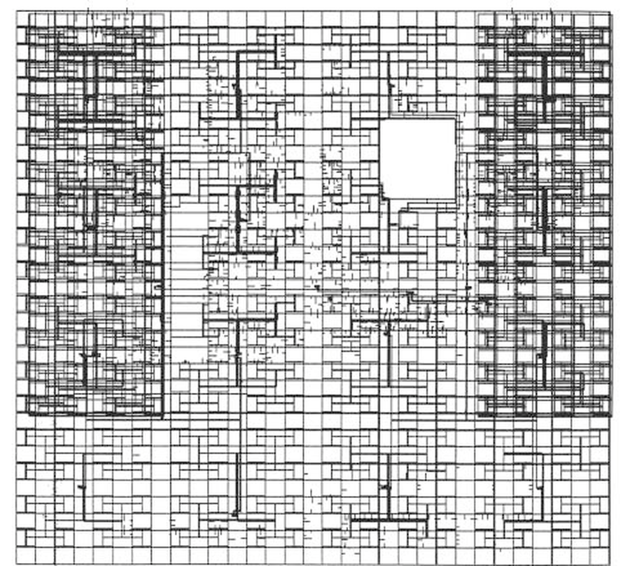
The problem is to ensure that the clock arrives at all circuits at the same time, minimizing "clock skew". Modern processors can reduce the clock skew to a few picoseconds. The clock is typically distributed by a "clock tree", where the clock is split into branches with each branch buffered and the same length, so the delays nearly match. One approach is an "H-tree", which distributes the clock through an H-shaped path. Each leg of the H branches into a smaller H recursively, forming a space-filling fractal, as shown below.

Clock distribution in a PowerPC chip. The recursive H pattern is only approximate since other layout factors constrain the clock tree. From ISSCC 2000.

Clock distribution in a PowerPC chip. The recursive H pattern is only approximate since other layout factors constrain the clock tree. From ISSCC 2000.

Delay circuitry can actively compensate for differences in path time. A Delay-Locked Loop (DLL) circuit adds variable delays to counteract variations along different clock paths. The Itanium used a clock distribution hierarchy with global, regional, and local distribution of the clock. The main clock was distributed to eight regions that each deskewed the clock (in 8.5 ps steps) and drove a regional clock grid, keeping the clock skew under 28 ps. The Pentium 4's complex distribution tree and skew compensation circuitry got clock skew below ±8 ps.

Conclusions

The 386's clock circuitry turned out to be more complicated than I expected, with a lot of subtlety and complications. However, examining the circuit illustrates several features of CMOS design, from latch circuits and high-current drivers to guard rings and multi-phase clocks. Hopefully you have found this interesting.

I plan to write more about the 386, so follow me on Twitter @kenshirriff or RSS for updates. I'm also on Mastodon occasionally as @[email protected].

Thanks to William Jones for discussing a couple of errors.

Notes and references

  1. You might wonder why processors use transparent latches and two clock phases instead of using edge-triggered flip-flops and a single clock phase. First, edge-triggered flip-flops take at least twice as many transistors as latches. (An edge-triggered flip flop is often built from two latch stages.) Second, the two-phase approach allows processing to happen twice per clock cycle, rather than once per clock cycle. This may allow a faster implementation with more pipelining. 

  2. The transparent latch was implemented by a single pass transistor in processors such as the MOS 6502. When the transistor was on, the input signal passed through. But when the transistor was off, the former value was held by the transistor's gate capacitance. Eventually the charge on the gate would leak away (like DRAM), so a minimum clock speed was required for reliable operation. 

  3. To see why having multiple stages active at once is bad, here's a simplified example. Consider a circuit that increments the accumulator register. In the first clock phase, the accumulator's value might go through the adder circuit. In the second clock phase, the new value can be stored in the accumulator. If both clock phases are high at the same time, the circuit will form a loop and the accumulator will get incremented multiple times, yielding the wrong result. Moreover, different parts of the adder probably have different delays, so the result is likely to be complete garbage. 

  4. To generate the clocks for the Intel 8008 processor, the suggested circuit used four analog (one-shot) delays to generate the clock phases. The 8008 and 8080 required asymmetrical clocks because the two blocks of logic took different amounts of time to process their inputs. The asymemtrical clock minimized wasted time, improving performance. (More discussion here.) 

  5. You might think that the 386 could use two clock signals: one latch could use phase 1 for NMOS and phase 2 for PMOS, while the next stage is the other way around. Unfortunately, that won't work because the two phases aren't exactly complements. During the "dead time" when phase 1 and phase 2 are both low, the PMOS transistors for both stages will turn on, causing problems. 

  6. Even though the 80386 has four clock signals internally, there are really just two clock phases. This is different from four-phase logic, a type of logic that was used in the late 1960s in some MOS processor chips. Four-phase logic was said to provide 10 times the density, 10 times the speed, and 1/10 the power consumption of standard MOS logic techniques. Designer Lee Boysel was a strong proponent of four-phase logic, forming the company Four Phase Systems and building a processor from a small number of MOS chips. Improvements in MOS circuitry in the 1970s (in particular depletion-mode logic) made four-phase logic obsolete. 

  7. The clocking scheme in the 386 is closely tied to the latch circuit used in the processor, shown below. This is a transparent latch: when enable is high and the complemented enable is low, the input is passed through to the output (inverted). When enable is low and the complemented enable is high, the latch remembers the previous value. The important factor is that the enable and complemented enable inputs must switch in lockstep. (In comparison, earlier chips such as the 8086 used a dynamic latch built from one transistor that used a single enable input.)

    The basic latch circuit used in the 386.

    The basic latch circuit used in the 386.

    The circuit on the right shows the implementation of the 386 latch. The two transistors on the left form a transmission gate: when both transistors are on, the input is passed through, but when both transistors are off, the input is blocked. Data storage is implemented through the two inverters connected in a loop. The bottom inverter is "weak", generating a small output current. Because of this, its output will be overpowered by the input, replacing the value stored in the latch. This latch uses 6 transistors in total.

    The 386 uses several variants of the latch circuit, for instance with set or reset inputs, or multiplexers to select multiple data inputs. 

  8. The parasitic transistors responsible for latch-up can also be viewed as an SCR (silicon-controlled rectifier) or thyristor. An SCR is a four-layer (PNPN) silicon device that is switched on by its gate and remains on until power is removed. SCRs were popular in the 1970s for high-current applications, but have been replaced by transistors in many cases. 

  9. The 386 uses two guard rings to prevent latch-up. NMOS transistors are surrounded by an inner N+ guard ring connected to ground and an outer P+ guard ring connected to +5. The guard rings are reversed for PMOS transistors. This page has a diagram showing how the guard rings prevent latch-up. 

  10. The polysilicon resistor appears to be unique to the clock input. My hypothesis is that the CLK2 signal runs at a much higher frequency than other inputs (since it is twice the clock frequency), which raises the risk of ringing or other transients. If these transients go below ground, they could cause latch-up, motivating additional protection on the clock input. 

  11. To keep the main article focused, I'll describe the inverters in this footnote. The circuitry below is between the divider logic and the polysilicon resistor, and consists of six inverters of various sizes. The large inverters 1 and 2 buffer the output from the divider to send to the drivers. Inverter 3 is a small inverter that drives larger inverter 4. I think this clock signal goes to the bus interface logic, perhaps to ensure that communication with the outside world is synchronized with the external clock, rather than the internal clock, which is shaped and perhaps slightly delayed. The output of small inverter 5 appears to be unused. My hypothesis is that this is a "dummy" inverter to match inverter 3 and ensure that both clock phases have identical circuitry. Otherwise, the load from inverter 3 might make that phase switch slightly slower.

    The inverters that buffer the divider's output.

    The inverters that buffer the divider's output.

    The final block of logic is shown below. This logic appears to take the chip reset signal from the reset pin and synchronize it with the clock. The first three latches use the CLK2 input as the clock, while the last two latches use the internal clock. Using the external reset signal directly would risk metastability because the reset signal could change asynchronously with respect to the rest of the system. The latches ensure that the timing of the reset signal matches the rest of the system, minimizing the risk of metastability. The NAND gate generates a reset pulse that resets the divide-by-two counter to ensure that it starts in a predictable state.

    The reset synchronizer. (Click for a larger image.)

    The reset synchronizer. (Click for a larger image.)


  12. The gate (2) that receives the inhibit signal is a bit strange, a cross between an inverter and a NAND gate. The gate goes low if the clk' input is high, but goes high only if both inputs are low. In other words, it acts like an inverter but the inhibit signal blocks the transition to the high output. Instead, the output will "float" with its previous low value. This will keep the driver's output low, ensuring that it doesn't overlap with the other driver's high output.

    The upper driver has a similar gate (4), except the extra input (enable) is on the NMOS side so the polarity is reversed. That is, the enable input must be high in order for the inverter to go low. 

  13. An interesting 2004 presentation is Clocking for High Performance Processors. A 2005 Intel presentation also discusses clock distribution.