Showing posts with label intel. Show all posts

The Pentium as a Navajo weaving

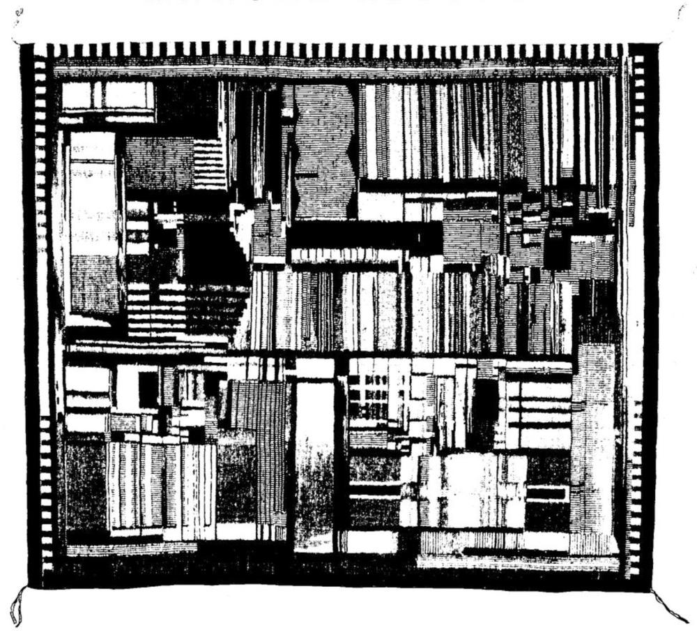
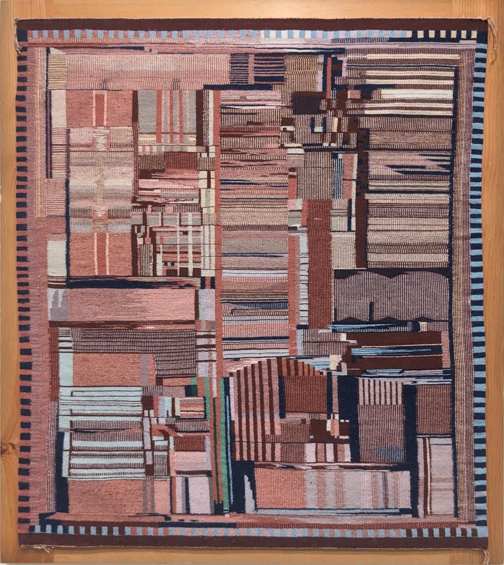
Hurrying through the National Gallery of Art five minutes before closing, I passed a Navajo weaving with a complex abstract pattern. Suddenly, I realized the pattern was strangely familiar, so I stopped and looked closely. The design turned out to be an image of Intel's Pentium chip, the start of the long-lived Pentium family.1 The weaver, Marilou Schultz, created the artwork in 1994 using traditional materials and techniques. The rug was commissioned by Intel as a gift to AISES (American Indian Science & Engineering Society) and is currently part of an art exhibition—Woven Histories: Textiles and Modern Abstraction—focusing on the intersection between abstract art and woven textiles.

"Replica of a Chip", created by Marilou Schultz, 1994. Wool. Photo taken at the National Gallery of Art, 2024.

"Replica of a Chip", created by Marilou Schultz, 1994. Wool. Photo taken at the National Gallery of Art, 2024.

I talked with Marilou Schultz, a Navajo/Diné weaver and math teacher, to learn more about the artwork. Schultz learned weaving as a child—part of four generations of weavers—carding the wool, spinning it into yarn, and then weaving it. For the Intel project, she worked from a photograph of the die, marking it into 64 sections along each side so the die pattern could be accurately transferred to the weaving. Schultz used the "raised outline" technique, which gives a three-dimensional effect along borders. One of the interesting characteristics of the Pentium from the weaving perspective is its lack of symmetry, unlike traditional rugs. The Pentium weaving was colored with traditional plant dyes; the cream regions are the natural color of the wool from the long-horned Navajo-Churro sheep.2 The yarn in the weaving is a bit finer than the yarn typically used for knitting. Weaving was a slow process, with a day's work extending the rug by 1" to 1.5".

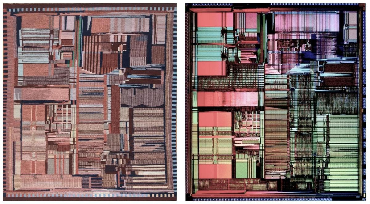
The Pentium die photo below shows the patterns and structures on the surface of the fingernail-sized silicon die, over three million tiny transistors. The weaving is a remarkably accurate representation of the die, reproducing the processor's complex designs. However, I noticed that the weaving was a mirror image of the physical Pentium die; I had to flip the rug image below to make them match. I asked Ms. Schultz if this was an artistic decision and she explained that she wove the rug to match the photograph. There is no specific front or back to a Navajo weaving because the design is similar on both sides,3 so the gallery picked an arbitrary side to display. Unfortunately, they picked the wrong side, resulting in a backward die image. This probably bothers nobody but me, but I hope the gallery will correct this in future exhibits. For the remainder of this article, I will mirror the rug to match the physical die.

Comparison of the Pentium weaving (flipped vertically) with a Pentium die photo. Original die photo from Intel.

Comparison of the Pentium weaving (flipped vertically) with a Pentium die photo. Original die photo from Intel.

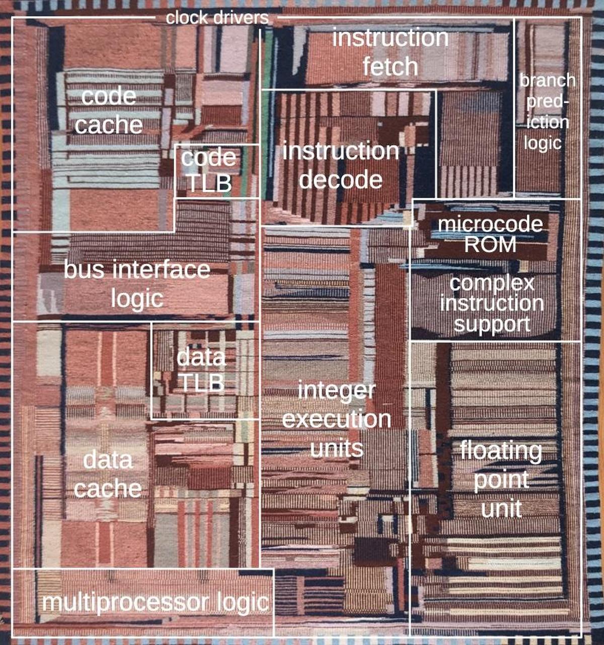
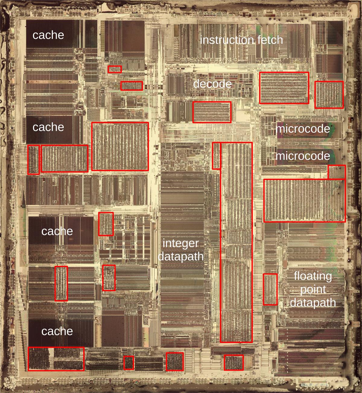
The rug is accurate enough that each region can be marked with its corresponding function in the real chip, as shown below. Starting in the center, the section labeled "integer execution units" is the heart of the processor, performing arithmetic operations and other functions on integer numbers. The Pentium is a 32-bit processor, so the integer execution unit is a vertical rectangle, 32 bits wide. The horizontal lines correspond to different types of circuitry such as adders, multipliers, shifters, and registers. To the right, the "floating point unit" performs more complex arithmetic operations on floating-point numbers, numbers with a fractional part that are used in applications such as spreadsheets and CAD drawings. Like the integer execution unit, the floating point unit has horizontal stripes corresponding to different functions. Floating-point numbers are represented with more bits, so the stripes are wider.

The Pentium weaving, flipped and marked with the chip floorplan.

The Pentium weaving, flipped and marked with the chip floorplan.

At the top, the "instruction fetch" section fetches the machine instructions that make up the software. The "instruction decode" section analyzes each instruction to determine what operations to perform. Simple operations, such as addition, are performed directly by the integer execution unit. Complicated instructions (a hallmark of Intel's processors) are broken down into smaller steps by the "complex instruction support" circuitry, with the steps held in the "microcode ROM". The "branch prediction logic" improves performance when the processor must make a decision for a branch instruction.

The code and data caches provide a substantial performance boost. The problem is that the processor is considerably faster than the computer's RAM memory, so the processor can end up sitting idle until program code or data is provided by memory. The solution is the cache, a small, fast memory that holds bytes that the processor is likely to need. The Pentium processor had a small cache by modern standards, holding 8 kilobytes of code and 8 kilobytes of data. (In comparison, modern processors have multiple caches, with hundreds of kilobytes in the fastest cache and megabytes in a slower cache.) Cache memories are built from an array of memory storage elements in a structured grid, visible in the rug as uniform pink rectangles. The TLB (Translation Lookaside Buffer) assists the cache. Finally, the "bus interface logic" connects the processor to the computer's bus, providing access to memory and peripheral devices. Around the edges of the physical chip, tiny bond pads provide the connections between the silicon chip and the integrated circuit package. In the weaving, these tiny pads have been abstracted into small black rectangles.

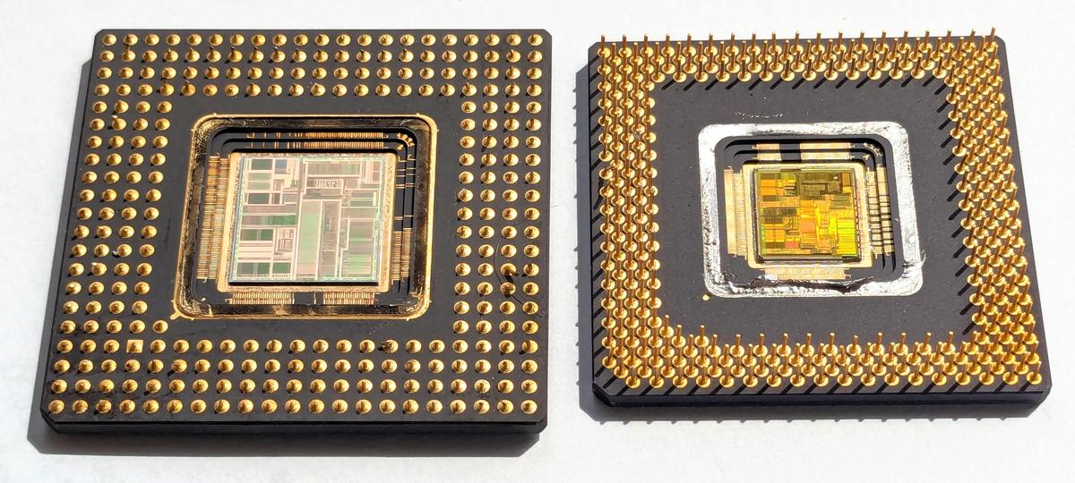
The weaving is accurate enough to determine that it represents a specific Pentium variant, called P54C. The motivation for the P54C was that the original Pentium chips (called P5) were not as fast as hoped and ran hot. Intel fixed this by using a more advanced manufacturing process, reducing the feature size from 800 to 600 nanometers and running the chip at 3.3 volts instead of 5 volts. Intel also modified the chip so that when parts of the chip were idle, the clock signal could be stopped to save power. (This is the "clock driver" circuitry at the top of the weaving.) Finally, Intel added multiprocessor logic (adding 200,000 more transistors), allowing two processors to work together more easily. The improved Pentium chip was smaller, faster, and used less power. This variant was called the P54C (for reasons I haven't been able to determine). The "multiprocessor logic" is visible in the Pentium rug, showing that it is the P54C Pentium (right) and not the P5 Pentium (left).

The Pentium P5 on the left and the P54C on the right, showing the difference in die and package sizes. If you look closely, the P5 die on the left lacks the "multiprocessor logic" in the weaving, showing that the weaving is the P54C. I clipped the pins on the P5 to fit it under a microscope.

The Pentium P5 on the left and the P54C on the right, showing the difference in die and package sizes. If you look closely, the P5 die on the left lacks the "multiprocessor logic" in the weaving, showing that the weaving is the P54C. I clipped the pins on the P5 to fit it under a microscope.

Intel's connection with New Mexico started in 1980 when Intel opened a chip fabrication plant (fab) in Rio Rancho, a suburb north of Albuquerque. At the time, this plant, Fab 7, was Intel's largest and produced 70% of Intel's profits. Intel steadily grew the New Mexico facility, adding Fab 9 and then Fab 11, which opened in September 1995, building Pentium and Pentium Pro chips in a 140-step manufacturing process. Intel's investment in Rio Rancho has continued with a $4 billion project underway for Fab 9 and Fab 11x. Intel has been criticized for environmental issues in New Mexico, detailed in the book Intel inside New Mexico: A case study of environmental and economic injustice. Intel, however, claims a sustainable future in New Mexico, restoring watersheds, using 100% renewable electricity, and recycling construction waste.

Fairchild and Shiprock

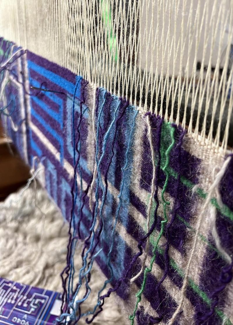
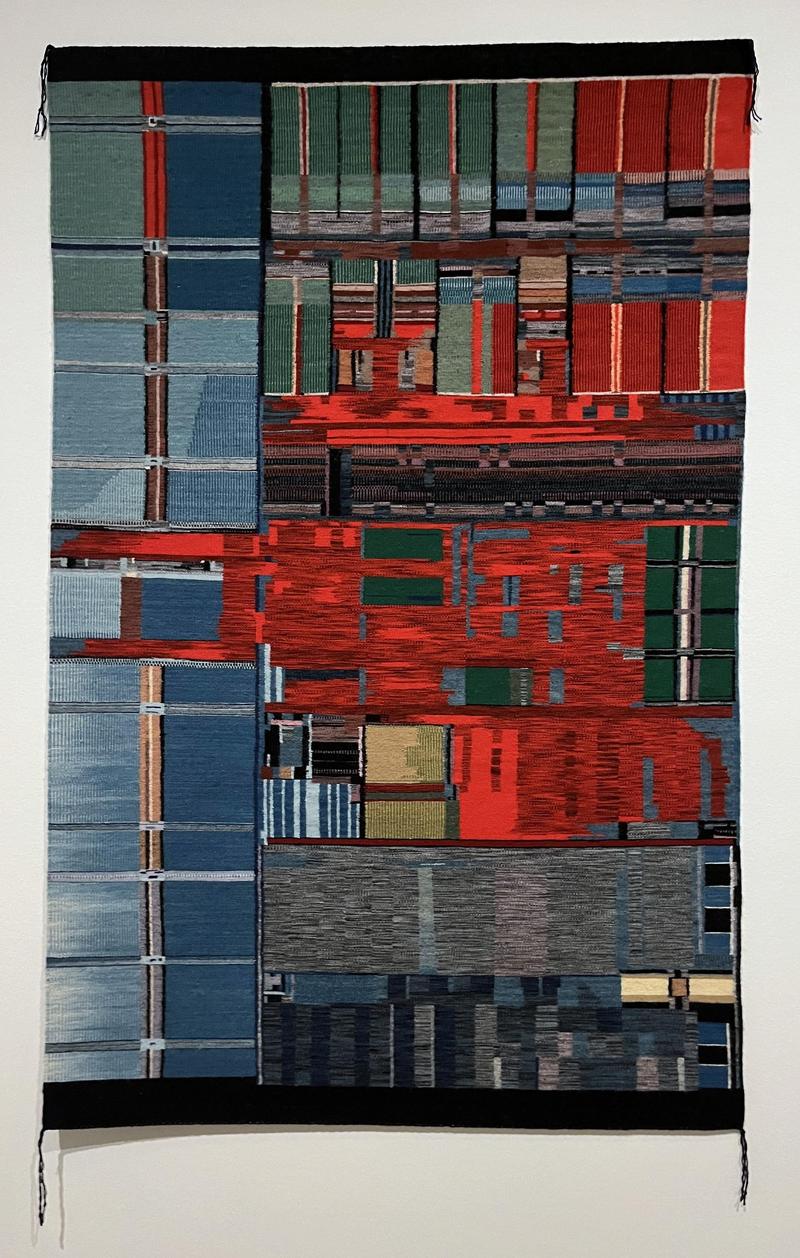
Marilou Schultz is currently creating another weaving based on an integrated circuit, shown below. Although this chip, the Fairchild 9040, is much more obscure than the Pentium, it has important historical symbolism, as it was built by Navajo workers at a plant on Navajo land.

Marilou Schultz's current weaving project. Photo provided by the artist.

Marilou Schultz's current weaving project. Photo provided by the artist.

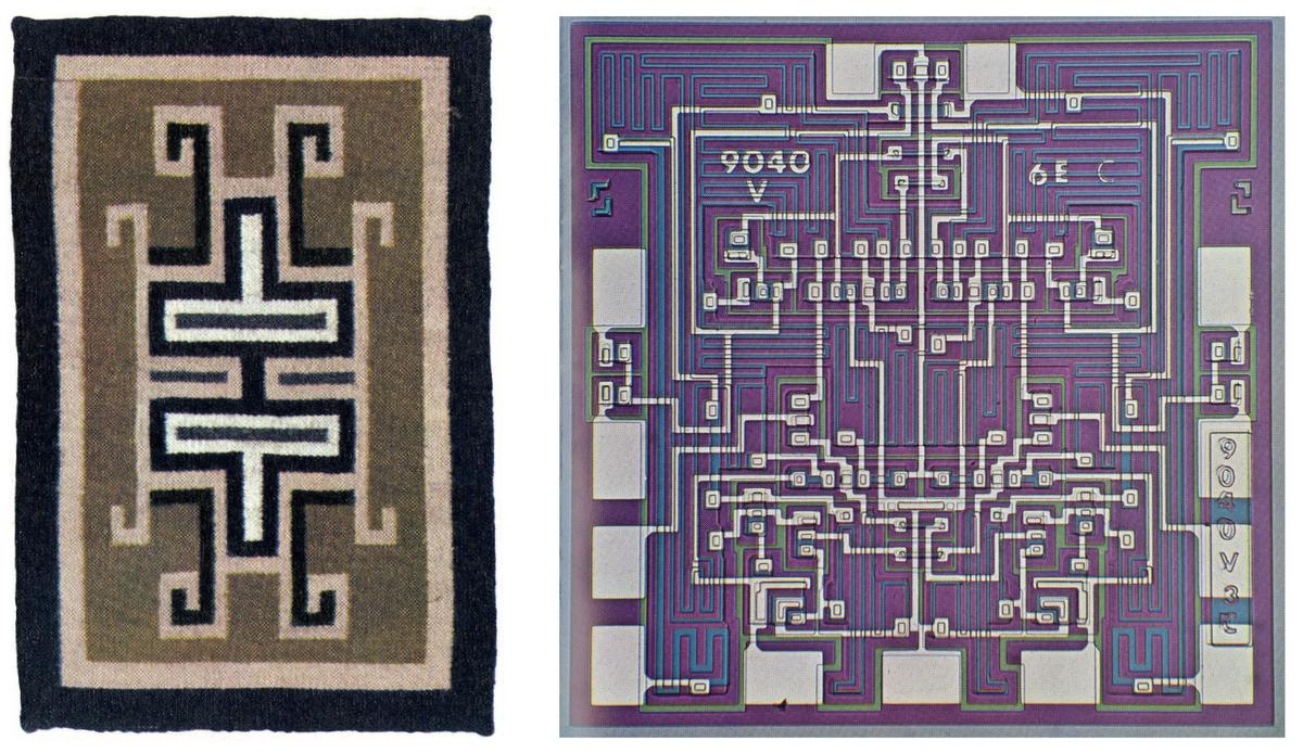
In 1965, Fairchild started producing semiconductors in Shiprock, New Mexico, about 200 miles northwest of Intel's future facility. Fairchild produced a brochure in 1969 to commemorate the opening of a new plant. Two of the photos in that brochure compared a traditional Navajo weaving to the pattern of a chip, which happened to be the 9040. Although Fairchild's Shiprock project started optimistically, it was suddenly shut down a decade later after an armed takeover. I'll discuss the complicated history of Fairchild in Shiprock and then describe the 9040 chip in more detail.

A Navajo rug and the die of a Fairchild 9040 integrated circuit. Images from Fairchild's commemorative brochure on the opening of a new plant at Shiprock.

A Navajo rug and the die of a Fairchild 9040 integrated circuit. Images from Fairchild's commemorative brochure on the opening of a new plant at Shiprock.

The story of Fairchild starts with William Shockley, who invented the junction transistor at Bell Labs, won the Nobel prize, and founded Shockley Semiconductor Laboratory in 1957 to build transistors. Unfortunately, although Shockley was brilliant, he was said to be the worst manager in the history of electronics, not to mention a notorious eugenicist and racist later in life. Eight of his top employees—called the "traitorous eight"—left Shockley's company in 1957 to found Fairchild Semiconductor. (The traitorous eight included Gordon Moore and Robert Noyce who ended up founding Intel in 1968). Noyce (co-)invented the integrated circuit in 1959 and Fairchild soon became a top semiconductor manufacturer, famous for its foundational role in Silicon Valley.

The Shiprock project was part of an attempt in the 1960s to improve the economic situation of the Navajo through industrial development. The Navajo had suffered a century of oppression including forced deportation from their land through the Long Walk (1864-1866). The Navajo were suffering from 65% unemployment, a per-capita income of $300, and a lack of basics such as roads, electricity, running water, and health care. The Bureau of Indian Affairs was now trying to encourage economic self-sufficiency by funding industrial projects on Indian land.4 Navajo Tribal Chairman Raymond Nakai viewed industrialization as the only answer. Called "the first modern Navajo political leader", Nakai stated, "There are some would-be leaders of the tribe calling for the banishment of industry from the reservation and a return to the life of a century ago! But, it would not solve the problems. There is not sufficient grazing land on the reservation to support the population so industry must be brought in." Finally, Fairchild was trying to escape the high cost of Silicon Valley labor by opening plants in low-cost locations such as Maine, Australia, and Hong Kong.

These factors led Fairchild to open a manufacturing facility on Navajo land in Shiprock, New Mexico. The project started in 1965 with 50 Navajo workers in the Shiprock Community Center manufacturing transistors, rapidly increasing to 366 Navajo workers.

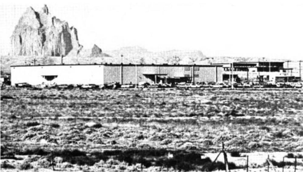
Fairchild's manufacturing plant in Shiprock, NM, named after the Shiprock rock formation in the background. The formation is called Tsé Bitʼaʼí in Navajo.
    From The Industrialization of a 'Sleeping Giant', Commerce Today, January 25, 1971.

Fairchild's manufacturing plant in Shiprock, NM, named after the Shiprock rock formation in the background. The formation is called Tsé Bitʼaʼí in Navajo. From The Industrialization of a 'Sleeping Giant', Commerce Today, January 25, 1971.

By 1967, Robert Noyce, group vice-president of Fairchild, regarded the Shiprock plant as successful. He explained that Fairchild was motivated both by low labor costs and by social benefits, saying, "Probably nobody would ever admit it, but I feel sure the Indians are the most underprivileged ethnic group in the United States." Two years later, Lester Hogan, Fairchild's president, stated, "I thought the Shiprock plant was one of Bob Noyce's philanthropies until I went there," but he was so impressed that he decided to expand the plant. Hogan also directed Fairchild to help build hundreds of houses for workers; since a traditional Navajo dwelling is called a hogan, the houses were dubbed Hogan's hogans.

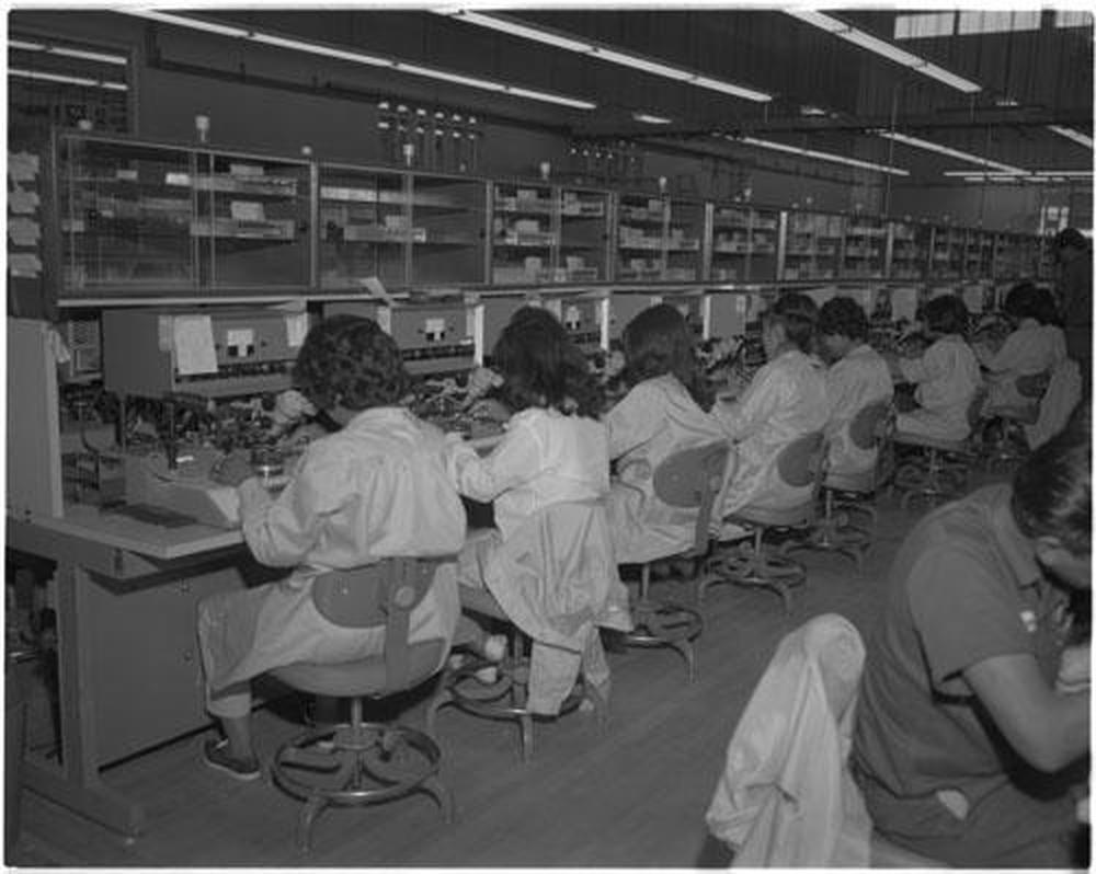
Workers in Fairchild's Shiprock plan, 1966. Photo by Jack Grimes. Photo courtesy of Computer History Museum, Henry Mahler collection of Fairchild Semiconductor photographs.

Workers in Fairchild's Shiprock plan, 1966. Photo by Jack Grimes. Photo courtesy of Computer History Museum, Henry Mahler collection of Fairchild Semiconductor photographs.

In 1969, Fairchild opened its new facility at Shiprock and produced the commemorative brochure mentioned earlier. As well as showing the striking visual similarity between the designs of traditional Navajo weavings and modern integrated circuits, it stated that "Weaving, like all Navajo arts, is done with unique imagination and craftsmanship" and described the "blending of innate Navajo skill and [Fairchild] Semiconductor's precision assembly techniques." Fairchild later said that "rug weaving, for instance, provides an inherent ability to recognize complex patterns, a skill which makes memorizing integrated circuit patterns a minimal problem."7

However, in Indigenous Circuits: Navajo Women and the Racialization of Early Electronic Manufacture, digital media theorist Lisa Nakamura critiques this language as a process by which "electronics assembly work became both gendered and identified with specific racialized qualities".5 Nakamura points out how "Navajo women’s affinity for electronics manufacture [was described] as both reflecting and satisfying an intrinsic gendered and racialized drive toward intricacy, detail, and quality."

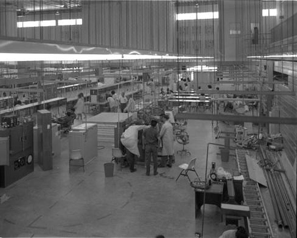
Fairchild's Shiprock plant, 1966. From the patterns on the floor, this photo may show the time period when Fairchild set up manufacturing in the school gymnasium. Photo by Jack Grimes. Photo courtesy of Computer History Museum, Henry Mahler collection of Fairchild Semiconductor photographs.

Fairchild's Shiprock plant, 1966. From the patterns on the floor, this photo may show the time period when Fairchild set up manufacturing in the school gymnasium. Photo by Jack Grimes. Photo courtesy of Computer History Museum, Henry Mahler collection of Fairchild Semiconductor photographs.

At Shiprock, Fairchild employed 1200 workers,6 and all but 24 were Navajo, making Fairchild the nation's largest non-government employer of American Indians. Of the 33 production supervisors, 30 were Navajo. This project had extensive government involvement from the Bureau of Indian Affairs and the U.S. Public Health Service, while the Economic Development Administration made business loans to Fairchild, the Labor Department had job training programs, and Housing and Urban Development built housing at Shiprock7.

The Shiprock plant was considered a major success story at a meeting of the National Council on Indian Opportunity in 1971.7 US Vice President Agnew called the economic deprivation and 40-80% unemployment on Indian reservations "a problem of staggering magnitude" and encouraged more industrial development. Fairchild President Hogan stated that "Fairchild's program at Shiprock has been one of the most rewarding in the history of our company, from the standpoint of a sound business as well as social responsibility." He said that at first the plant was considered the "Shiprock experiment", but the plant was "now among the most productive and efficient of any Fairchild operation in the world." Peter MacDonald, Chairman of the Navajo Tribal Council and a World War II Navajo code talker, discussed the extreme poverty and unemployment on the Navajo reservation, along with "inadequate housing, inadequate health care and the lack of viable economic activities." He referred to Fairchild as "one of the best arrangements we have ever had" providing not only employment but also supporting housing through a non-profit.

Navajo workers using microscopes in Fairchild's Shiprock plant. From "The Navajo Nation Looks Ahead", National Geographic, December 1972.

Navajo workers using microscopes in Fairchild's Shiprock plant. From "The Navajo Nation Looks Ahead", National Geographic, December 1972.

In December 1972, National Geographic highlighted the Shiprock plant as "weaving for the Space Age", stating that the Fairchild plant was the tribe's most successful economic project with Shiprock booming due to the 4.5-million-dollar annual payroll. The article states: "Though the plant runs happily today, it was at first a battleground of warring cultures." A new manager, Paul Driscoll, realized that strict "white man's rules" were counterproductive. For instance, many employees couldn't phone in if they would be absent, as they didn't have telephones. Another issue was the language barrier since many workers spoke only Navajo, not English. So when technical words didn't exist in Navajo, substitutes were found: "aluminum" became "shiny metal". Driscoll also realized that Fairchild needed to adapt to traditional nine-day religious ceremonies. Soon the monthly turnover rate dropped from 12% to under 1%, better than Fairchild's other plants.

Unfortunately, the Fairchild-Navajo manufacturing partnership soon met a dramatic end. In 1975, the semiconductor industry was suffering from the ongoing US recession. Fairchild was especially hard hit, losing money on its integrated circuits, and it shed over 8000 employees between 1973 and 1975.8 At the Shiprock plant, Fairchild laid off9 140 Navajo employees in February 1975, angering the community. A group of 20 Indians armed with high-power rifles took over the plant, demanding that Fairchild rehire the employees. Fairchild portrayed the occupiers, part of the AIM (American Indian Movement), as an "outside group—representing neither employees, tribal authorities nor the community." Peter MacDonald, chairman of the Navajo Nation, agreed with the AIM on many points but viewed the AIM occupiers as "foolish" with "little sense of Navajo history" and "no sense of the need for an Indian nation to grow" (source). MacDonald negotiated with the occupiers and the occupation ended peacefully a week later, with unconditional amnesty granted to the occupiers.10 However, concerned about future disruptions, Fairchild permanently closed the Shiprock plant and transferred production to Southeast Asia.

An article entitled "Navajos Occupy Plant". Contrary to the title, MacDonald stated that many of the occupiers were from other tribes and were not acting in the best interest of the Navajo. From Workers' Power, the biweekly newspaper of the International Socialists, March 13-26, 1975.

An article entitled "Navajos Occupy Plant". Contrary to the title, MacDonald stated that many of the occupiers were from other tribes and were not acting in the best interest of the Navajo. From Workers' Power, the biweekly newspaper of the International Socialists, March 13-26, 1975.

For the most part, the Fairchild plant was viewed as a success prior to its occupation and closure. Navajo leader MacDonald looked back on the Fairchild plant as "a cooperative effort that was succeeding for everyone" (link). Alice Funston, a Navajo forewoman at Shiprock said, "Fairchild has not only helped women get ahead, it has been good for the entire Indian community in Shiprock."11 On the other hand, Fairchild general manager Charles Sporck had a negative view looking back: "It [Shiprock] never worked out. We were really screwing up the whole societal structure of the Indian tribe. You know, the women were making money and the guys were drinking it up. We had a very major negative impact upon the Navajo tribe."12

Despite the stereotypes in Sporck's comments, he touches on important gender issues, both at Fairchild and in the electronics industry as a whole. Fairchild had long recognized the lack of jobs for men at Shiprock, despite attempts to create roles for men. In 1971, Fairchild President Hogan stated that since "semiconductor assembly operation require a great amount of detail work with tiny components, [it] lends itself to female workers. As a result, there are nearly three times as many Navajo women employed by Fairchild as men."7

The role of women in fabricating and assembling electronics is often not recognized. A 1963 report on electronics manufacturing estimated that women workers made up 41 percent of total employment in electronics manufacturing, largely in gendered roles. The report suggested that microminiaturization of semiconductors gave women an advantage over men in assembly and production-line work; women made up over 70% of semiconductor production-line workers, with 90-99% of inspecting and testing jobs. and 90-100% of assembler jobs. Women were largely locked out of non-production jobs; although women held a few technician and drafting roles, the percentage of woman engineers was too low to measure.

The defense contractor General Dynamics also had Navajo plants, but with more success than Fairchild. General Dynamics opened a Navajo Nation plant in Fort Defiance, Arizona in 1967 to make missiles for the Navy. At the plant's opening, Navajo Tribal Chairman Raymond Nakai pushed for industrialization, stating that it was in "industrialization and the money and the jobs engendered thereby that the future of the Navajo people will lie." The plant started with 30 employees, growing to 224 by the end of 1969, but then dropping to 99 in 1971 due to a slowdown in the electronics industry. General Dynamics opened another Navajo plant near Farmington NM in 1988. Due to the end of the Cold War, Hughes Aircraft (part of General Motors) acquired General Dynamics' missile business in 1992 and sold it to Raytheon in 1997. The Fort Defiance facility was closed in 2002 when its parent company, Delphi Automotive Systems, moved out of the military wiring business. The Farmington plant remains open, now Raytheon Diné, building components for Tomahawk, Javelin, and AMRAAM missiles.

Navajo workers at the General Dynamics plant in Fort Defiance, AZ. From the 1965 General Dynamics film "The Navajo moves into the electronic age". From American Indian Film Gallery.

Navajo workers at the General Dynamics plant in Fort Defiance, AZ. From the 1965 General Dynamics film "The Navajo moves into the electronic age". From American Indian Film Gallery.

Inside the Fairchild 9040 integrated circuit

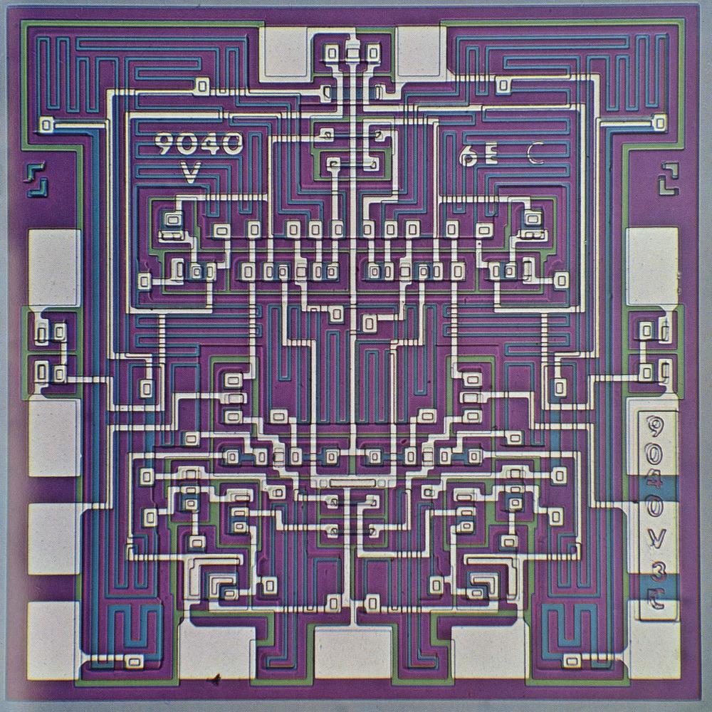
The integrated circuit die image in Fairchild's commemorative brochure has an exceptionally striking design and color scheme. It's clear why this chip brings weaving to mind. Studying the die photo of the 9040 carefully reveals some interesting characteristics of integrated circuit design, so I will go into some detail.

Die photo of the Fairchild 9040 flip-flop. From the commemorative brochure.

Die photo of the Fairchild 9040 flip-flop. From the commemorative brochure.

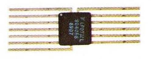
The chip was fabricated from a tiny square of silicon, which appears purple in the photograph. Different regions of the silicon die were treated (doped) with impurities to change the properties of the silicon and thus create electronic devices. These doped regions appear as green or blue lines. The white lines are the metal layer on top of the silicon, connecting the components. The 13 metal rectangles around the border are the bond pads. The chip was packaged in an unusual 13-pin flat-pack, as shown below. Each of the 13 bond pads above was connected by a tiny wire to one of the 13 external pins.

The Fairchild 9040 packaged in a 13-pin flatpack integrated circuit. The chip was also available in a 14-pin DIP, a standard way of packaging chips. Photo from the commemorative brochure.

The Fairchild 9040 packaged in a 13-pin flatpack integrated circuit. The chip was also available in a 14-pin DIP, a standard way of packaging chips. Photo from the commemorative brochure.

The Fairchild 9040 was introduced in the mid-1960s as part of Fairchild's Micrologic family, a set of high-performance integrated circuits that were designed to work together.13 The 9040 chip was a "flip-flop", a circuit capable of storing a single bit, a 0 or 1. Flip-flops can be combined to form counters, counting the number of pulses, for instance.

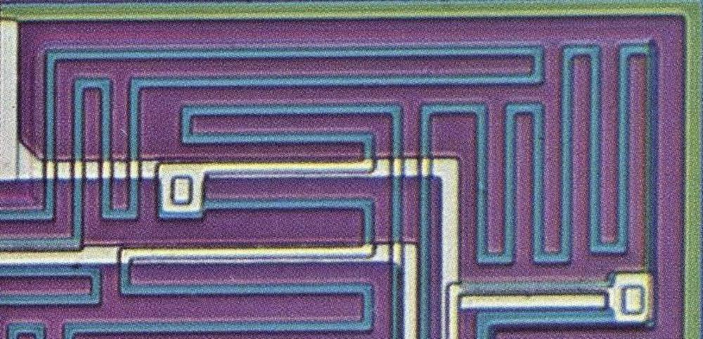
The most dramatic patterns on the chip are the intricate serpentine blue lines. Each line forms a resistor, controlling the flow of electricity by impeding its path. The lines must be long to provide the desired resistance, so they wind back and forth to fit into the available space. Each end of a resistor is connected to the metal layer, wiring it to another part of the circuit. Most of the die is occupied by resistors, which is a disadvantage of this type of circuit. Modern integrated circuits use a different type of circuitry (CMOS), which is much more compact, partly because it doesn't need bulky resistors.

Resistors in the 9040 die.

Resistors in the 9040 die.

Transistors are the main component of an integrated circuit. These tiny devices act as switches, turning signals on and off. The photo below shows one of the transistors in the 9040. It consists of three layers of silicon, with metal wiring connected to each layer. Note the blue region in the middle, surrounded by a slightly darker purple region; these color changes indicate that the silicon has been doped to change its properties. The green region surrounding the transistor provides isolation between this transistor and the other circuitry, so the transistors don't interfere with each other. The chip also has many diodes, which look similar to transistors except a diode has two connections.

A transistor in the 9040 die. The three contacts are called the base, emitter, and collector.

A transistor in the 9040 die. The three contacts are called the base, emitter, and collector.

These transistors with their three layers of silicon are a type known as bipolar. Modern computers use a different type of transistor, metal-oxide-semiconductor (MOS), which is much more compact and efficient. One of Fairchild's major failures was staying with bipolar transistors too long, rather than moving to MOS.14 In a sense, the photo of the 9040 die shows the seeds of Fairchild's failure.

The 9040 chip was constructed on a completely different scale from the Pentium, showing the rapid progress of the IC industry. The 9040 contains just 16 transistors, while the Pentium contains 3.3 million transistors. Thus, individual transistors can be seen in the 9040 image, while only large-scale functional blocks are visible in the Pentium. This increasing transistor count illustrates the exponential growth in integrated circuit capacity between the 9040 in the mid-1960s and the Pentium in 1993. This growth pattern, with the number of transistors doubling about every two years, is known as Moore's law, since it was first observed in 1965 by Gordon Moore (one of Fairchild's "traitorous eight", who later started Intel).

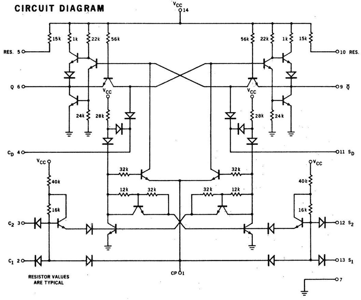
The schematic below shows the circuitry inside the 9040 chip, with its 16 transistors, 16 diodes, and 22 resistors. The symmetry of the 9040 die photo makes it appealing, and that symmetry is reflected in the circuit below, with the left side and the right side mirror images. The idea behind a flip-flop is that it can hold either a 0 or a 1. In the chip, this is implemented by turning on the right side of the chip to hold a 0, or the left side to hold a 1. If one side of the chip is on, it forces the other side off, accomplished by the X-like crossings of signals in the center.15 Thus, the symmetry is not arbitrary, but is critical to the operation of the circuit.

Schematic of the Fairchild 9040 flip-flop chip. From Fairchild 1970 Data Catalog.

Schematic of the Fairchild 9040 flip-flop chip. From Fairchild 1970 Data Catalog.

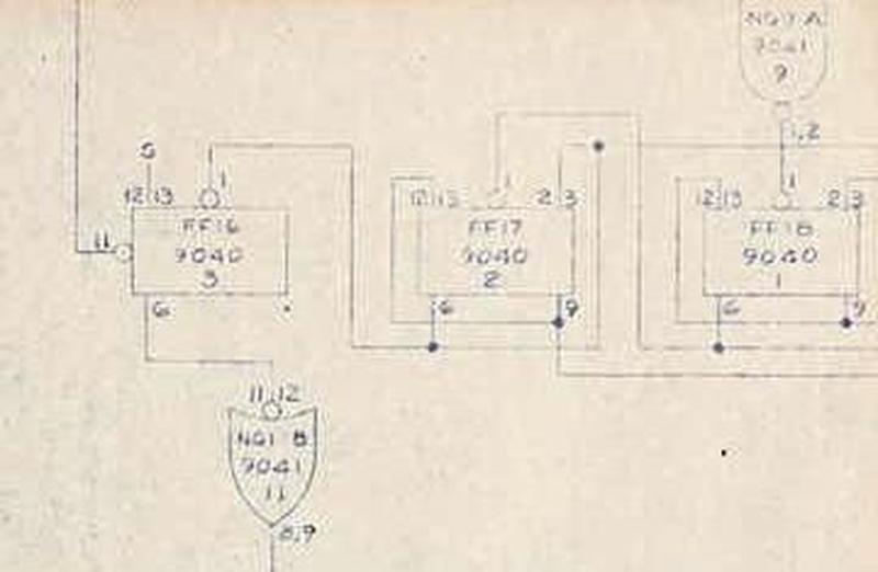
Despite the obscurity of the 9040, multiple 9040 chips are currently on the Moon. The chip was used in the Apollo Lunar Surface Experiments Package (ALSEP),16 in particular, the Active Seismic Experiment on Apollo 14 and 16. This experiment detonated small explosives on the Moon and measured the resulting seismic waves. The photo below is a detail from a blueprint17 that shows three of the nineteen 9040 flip-flops (labeled "FF") as well as two 9041 logic gates, a chip in the same family as the 9040.

Detail from Logic Schematic Type B Board No.4 ASE.

Detail from Logic Schematic Type B Board No.4 ASE.

Conclusions

The similarities between Navajo weavings and the patterns in integrated circuits have been described since the 1960s. Marilou Schultz's weavings of integrated circuits make these visual metaphors into concrete works of art. Although the Woven Histories exhibit at the National Gallery of Art is no longer on display, the exhibit will be at the National Gallery of Canada (Ottawa) starting November 8, 2024, and the Museum of Modern Art (New York) starting April 20, 2025 (full dates here). If you're in the area, I recommend viewing the exhibit, but don't make my mistake: leave more than five minutes to see it!

Many thanks to Marilou Schultz for discussing her art with me. For more on her art, see A Conversation with Marilou Schultz on YouTube.18 Follow me on Mastodon as @[email protected] or RSS for updates.

Notes and references

  1. The original Pentium was followed by the Pentium Pro, the Pentium II, and others, forming a long-running brand of high-performance processors. Pentium was Intel's flagship line until the Core processors took over in 2006. 

  2. Sheep hold a key role in Navajo culture and economy, which I'll briefly summarize here. Domestic sheep were brought to the Americas during the Spanish colonization, reaching the Navajo in the late 1500s. Since sheep were able to graze on semi-arid land unsuitable for crops, sheep became very important to the Navajo. Although the Navajo had used cotton for weaving in the past, the availability of wool made weaving a fundamental industry; the production and trading of woven Navajo blankets became an important economic factor in New Mexico by the 1750s (details).

    Navajo leader Peter MacDonald described the role of sheep: "Sheep were like money in the bank: the more you had, the better your life, your future, and your family's future." The number of sheep grew exponentially in the early 1900s, resulting in overgrazing of the land. The drought and Dust Bowl of the 1930s led the government to restrict the number of sheep on Navajo land, imposing the Navajo Livestock Reduction. This heavy-handed program purchased and slaughtered over half the livestock, which was catastrophic to the Navajo, both economically and culturally, destroying the Navajo's wealth and self-sufficiency.

    The Navajo-Churro sheep is a breed that the Navajo developed from the Churra sheep brought from Spain during the Spanish colonization of the Americas. These sheep have a long, lustrous fleece that is excellent for weaving. The Navajo-Churro is also called the Navajo Four-Horned Sheep as some rams have four horns, a rare trait. The Navajo-Churro breed was severely depleted when American troops killed livestock during the Navajo Wars (1863) and then brought close to extinction by the Livestock Reduction of the 1930s to 1950s. In the 1970s, the Navajo Sheep Project started efforts to preserve and revitalize the Navajo-Churro. The breed is still rare, but currently numbers in the thousands. Now, climate change and water shortages are putting more pressure on sheep grazing.  

  3. A photo of the rug was published in American Indian Science & Engineering Society 1994 Annual Report. This photo shows the "physically accurate" side of the rug, not the side that is currently on display.

    A photo of the rug from 1994.

    A photo of the rug from 1994.

    Which side of a die image is the top is mostly arbitrary. Intel usually presents die photos with the tiny text on the die right side up, so I will use that convention. For the Pentium die, this text is in the lower right corner and says "80P54C (m) (c) intel '92,'93". Of course, this text is much too small to be part of the woven rug. 

  4. Strengthening the Indian Economy (Indian Affairs, 1966) discusses various industrial development projects, of which Fairchild was the largest. Other projects included a plant at Rolla, ND to produce sapphire and ruby bearings, a Seminole project with Amphenol to produce electronic connectors, and a Hopi project with BVD to produce garments. Other economic development projects included timber and mining; extractive industries provided over half of Navajo income. 

  5. Racialization is defined by Nakamura as "the understanding of a specific population as possessing traits and behaviors that belong to a race, not an individual." 

  6. Many photos of workers at the Shiprock plant are in Fairchild VIEWS, March 1969. Fairchild deserves credit for referring to the workers by name rather than viewing them as anonymous props for photos. Fairchild followed the same practice in its annual reports

  7. NCIO (National Council on Indian Opportunity) News, Oct/Nov 1971 described a high-level meeting with industry to discuss "new development on Indian reservations" with industry. US Vice President Spiro Agnew ran the meeting, with Attorney General John Mitchell a speaker along with Navajo Tribal Council chairman Peter MacDonald. Bizarrely, all three ended up convicted of felonies for different reasons. Within a few years, Mitchell was imprisoned for Watergate crimes and Agnew pled guilty to federal tax evasion. In 1990, MacDonald was convicted of fraud, riot, extortion, racketeering, and conspiracy by a Navajo tribal judge and then a federal judge, spending eight years in prison until pardoned by Bill Clinton (details). The story of Peter MacDonald is complex and many view his prosecution as politically motivated; MacDonald's memoir provides his perspective. 

  8. Although Fairchild was highly successful at first, it suffered from chaotic management and economic decline. Fairchild steadily lost key employees, many of whom started competing companies. Most important was Intel, started in 1968 by Moore and Noyce, two of the "Traitorous Eight". Eventually, hundreds of companies (called the Fairchildren) could be traced back to Fairchild. Economic factors also battered Fairchild; the semiconductor industry had barely recovered from the 1970-1971 recession when it was hit by the severe 1975 recession. As a result, Fairchild had large layoffs, of which the Shiprock layoffs were a small part. Fairchild's business continued to decline; it was purchased by Schlumberger in 1979 and went through various acquisitions, mergers, and spinoffs until it finally ended in 2016, acquired by ON Semiconductor. 

  9. Were the employees "laid off" or "layed off"? Curiously, the New York Times article said "layed off" but sources uniformly state that "layed off" is grammatically wrong. The New York Times has extensively used "layed off" so this isn't a one-time typo. I hypothesized that usage had changed since the 1970s but Google Ngram Viewer shows laid off as the consistent and overwhelming winner. Maybe "layed off" was a stylistic quirk of the New York Times? 

  10. Looking back, MacDonald questioned his decision to let the occupation of Fairchild's plant continue rather than ordering the tribal police to forcibly remove the occupiers from the plant. In his view, his decision to let the occupation led to the closing of the plant and the loss of 1200 jobs. On the other hand, forcibly removing the occupiers risked violence and loss of life: "I would have become the chairman who killed his own people instead of the chairman who allowed Navajo to lose their jobs."

    The risk of bloodshed was not theoretical. In 1989, a riot between MacDonald's supporters and the police resulted in two Navajos being shot and killed by the police. MacDonald pressed for a federal investigation into police brutality, but instead MacDonald and Benally (a council delegate) received long prison sentences for inciting the riot even though they were not present at the time. 

  11. Alice Funston was Forewoman for the Reliability and Quality Assurance Section at Shiprock. In a Fairchild employee newsletter, she said, "Fairchild has not only helped women get ahead, it has been good for the entire Indian community in Shiprock. Before the plant was built here, there weren't many jobs available. You could work for the Bureau of Indian Affairs, the Navajo Tribe or other government agencies, but there just weren't enough jobs to go around. I started in assembly in 1965 and was recently promoted to Production Supervisor in R & Q.A. Since the beginning of the year, a number of women have been promoted into supervisory positions. When I joined Fairchild, most of the members of management were non-Indian. Today, almost all of our supervisors and managers are Indian."

    I quote this at length, since it was the only example I could find of an employee discussing Shiprock in their own words. It must be recognized, of course, that this is a company publication, so the comments may not be completely candid. See "Affirmative Action: A growing consciousness of the needs of the individual" in Fairchild HORIZONS, May-June, 1973. 

  12. See Interview with Charlie Sporck, 2000 February 21, timestamp 0:27. From "Silicon Genesis: oral history interviews of Silicon Valley scientists, 1995-2024," Stanford Digital Repository.

    I view Sporck's comments on the failure of Shiprock as highly questionable. First, Sporck left Fairchild in 1967, so he was not present for most of the Shiprock project. Moreover, he implies that Fairchild's closing of Shiprock was in the best interest of the Navajo, which is a morally convenient justification for Fairchild's decision, but contradicted by most other sources. 

  13. Fairchild's 9040 logic family was called LPDTμL for "low-power diode-transistor Micrologic". Some sources label this family as TTL (Transistor-Transistor Logic), probably confusing it with the 9000-family, which was TTL. 

  14. Fairchild's failure to recognize the importance of MOS transistors and transition from bipolar transistors is described in History of Semiconductor Engineering, page 170. 

  15. I'll provide more details of the 9040 schematic in this footnote. The 9040 is a flexible flip-flop. It can be wired as an R-S (reset-set) flip-flop, set to 1 or reset to 0 as needed. It can also be wired as a J-K flip-flop, a flexible circuit that can store a value, hold a value, or toggle, based on the settings of the J and K inputs.

    The 9040 is a "dual-rank" flip-flop, meaning it holds its value in two latches: a primary latch and a secondary latch. (This type of flip flop was generally called "master-slave", a name that is now controversial). Looking at the schematic, the primary latch at the bottom of the schematic passes its value to the secondary latch at the top under the control of the clock. This structure makes the flip-flop "edge-triggered", changing its value at the moment when the clock signal changes.

    This circuit uses diode-transistor logic. Diodes perform most of the logic operations by combining input signals, while the transistors provide amplification. Diodes play a different role in the "push-pull" output circuit, raising the level of the high-side transistor. Because the output circuit has a transistor, diode, and transistor stacked vertically, it is often called a totem pole output, a name that seems questionable in this context.

    One curious feature of the 9040 is that it contains two pull-up resistors that are not assigned any role. The user of the chip can attach them to unused inputs to keep the input at the desired value.

    Looking at the schematic shows 13 pins, corresponding to the 13 pins of the flat-pack integrated circuit. All but three of these pins are symmetrical; power (Vcc), ground, and the clock (CP) have single connections. The ground pad is in the bottom-center of the die, which maintains symmetry. The clock and power pads are side-by-side in the top-center of the die. If you study the die photograph closely, you will see that they subtlely break the chip's symmetry as the clock signal runs down the center of the die while the power connection runs down both sides. There are a few other subtle violations of symmetry when signals cross from one side of the chip to the other, as well as the obviously asymmetrical text. 

  16. I haven't been able to prove that the Apollo program used chips from the Shiprock plant rather than a different facility. Fairchild President Hogan stated that workers at Shiprock assembled guidance, communications, and gyro systems that were used on Apollo rockets. 

  17. The ALSEP schematic is from Miller, K. Logic Schematic Type B Board No.4 ASE, A4, technical drawing, January 27, 1967, University of North Texas Libraries, The Portal to Texas History; crediting Lunar Planetary Institute Library. 

  18. Marilou Schultz had another chip weaving on display at the National Gallery of Art. It is labeled "Untitled (Unknown Chip), 2008", but Antoine Bercovici identified it for me as the AMD K6 III processor, released in 1999 and comparable to the Pentium III.

    A weaving created by Marilou Schultz, "Untitled (Unknown Chip)".

    A weaving created by Marilou Schultz, "Untitled (Unknown Chip)".

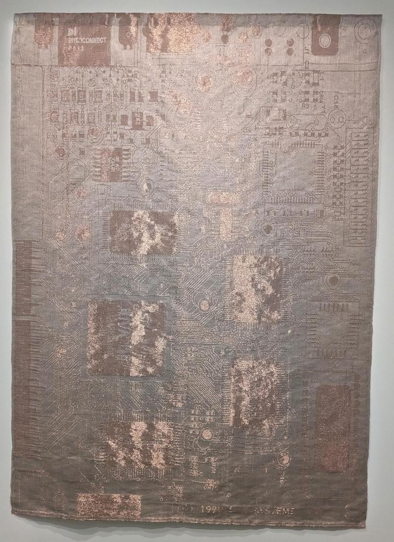
    If you're interested in computer-related weaving, the exhibition also had "Copper Tapestry (Riva 128 Graphics Card, Nvidia, 1997)" by Argentinian artist Analia Saban, created on a computer-automated Jacquard loom. This weaving represents a PC graphics card, specifically, the STB Velocity 128, which uses the Nvidia Riva 128 GPU chip. This chip was released in 1997, at a point when Nvidia was in a dire financial position, thirty days from going out of business. The Riva 128 saved Nvidia and now Nvidia is the world's third most valuable company.

    A tapestry created by Analia Saban, "Copper Tapestry (Riva 128 Graphics Card, Nvidia, 1997)".
    A tapestry created by Analia Saban, "Copper Tapestry (Riva 128 Graphics Card, Nvidia, 1997)".
     

Standard cells: Looking at individual gates in the Pentium processor

Intel released the powerful Pentium processor in 1993, a chip to "separate the really power-hungry folks from ordinary mortals." The original Pentium was followed by the Pentium Pro, the Pentium II, and others, spawning a long-running brand of high-performance processors, Intel's flagship line until the Core processors took over in 2006. The Pentium eventually became virtually synonymous with "PC" and even made it into pop culture.

Even though the Pentium is a complex chip with 3.3 million transistors, its transistors are visible under a microscope, unlike modern chips. By examining the chip, we can see the interesting circuits used for gates, flip-flops, and other circuits, including the use of an unusual technology called BiCMOS. In this article, I take a close look at the original Pentium chip1, showing how much of its circuitry was built out of structured rows of tiny transistors, a technique known as standard-cell design.

The die photo below shows the Pentium's fingernail-sized silicon die under a microscope. I removed the chip's four metal layers to show the underlying silicon, revealing the individual transistors, which are obscured in most die photos by the layers of metal. Standard-cell circuitry, indicated by red boxes, is recognizable because the circuitry is arranged in uniform columns of cells, giving it a characteristic striped appearance. In contrast, the chip's manually-optimized functional blocks are denser and more structured, giving them a darker appearance. Examples are the caches on the left, the datapaths in the middle, and the microcode ROMs on the right.

Die photo of the Intel Pentium processor with standard cells highlighted in red. The edges of the chip suffered some damage when I removed the metal layers. Click this image (or any other) for a larger version.

Die photo of the Intel Pentium processor with standard cells highlighted in red. The edges of the chip suffered some damage when I removed the metal layers. Click this image (or any other) for a larger version.

Standard-cell design

Early processors in the 1970s were usually designed by manually laying out every transistor individually, fitting transistors together like puzzle pieces to optimize their layout. While this was tedious, it resulted in a highly dense layout. Federico Faggin, designer of the popular Z80 processor, was almost done when he ran into a problem. The last few transistors wouldn't fit, so he had to erase three weeks of work and start over. The closeup of the resulting Z80 layout below shows that each transistor has a different, complex shape, optimized to pack the transistors as tightly as possible.2

A closeup of transistors in the Zilog Z80 processor (1976). This chip is NMOS, not CMOS, which provides more layout flexibility. The metal and polysilicon layers have been removed to expose the underlying silicon. The lighter stripes over active silicon indicate where the polysilicon gates were. I think this photo is from the Visual 6502 project but I'm not sure.

A closeup of transistors in the Zilog Z80 processor (1976). This chip is NMOS, not CMOS, which provides more layout flexibility. The metal and polysilicon layers have been removed to expose the underlying silicon. The lighter stripes over active silicon indicate where the polysilicon gates were. I think this photo is from the Visual 6502 project but I'm not sure.

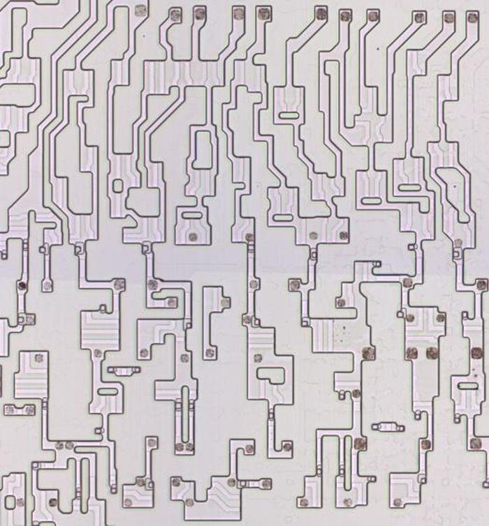
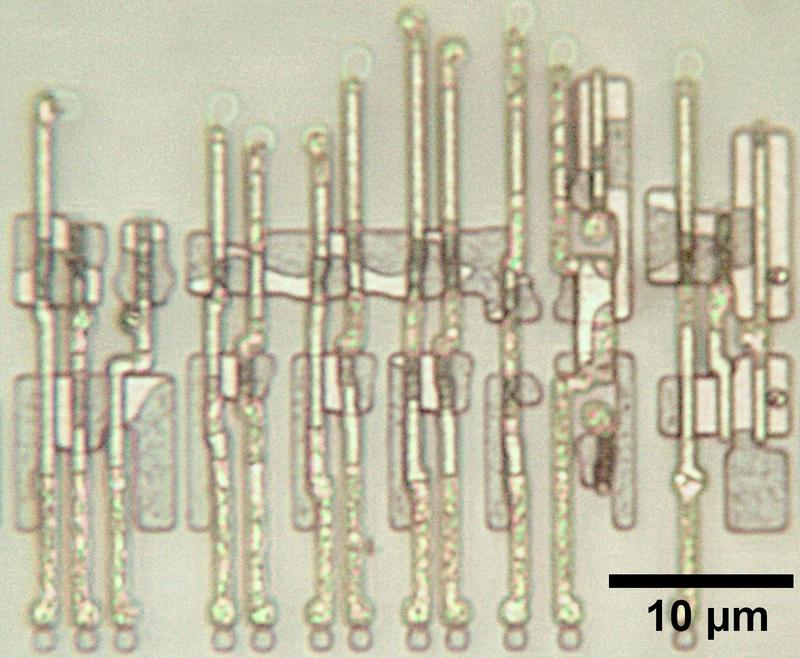
Because manual layout is slow, difficult, and error-prone, people developed automated approaches such as standard-cell.3 The idea behind standard-cell is to create a standard library of blocks (cells) to implement each type of gate, flip-flop, and other low-level component. To use a particular circuit, instead of arranging each transistor, you use the standard design from the library. Each cell has a fixed height but the width varies as needed, so the standard cells can be arranged in rows. The Pentium die photo below shows seven cells in a row. (The rectangular blobs are doped silicon while the long, thin vertical lines are polysilicon.) Compare the orderly arrangement of these transistors with the Z80 transistors above.

Some standard cell circuitry in the Pentium.
I removed the metal to show the underlying silicon and polysilicon.

Some standard cell circuitry in the Pentium. I removed the metal to show the underlying silicon and polysilicon.

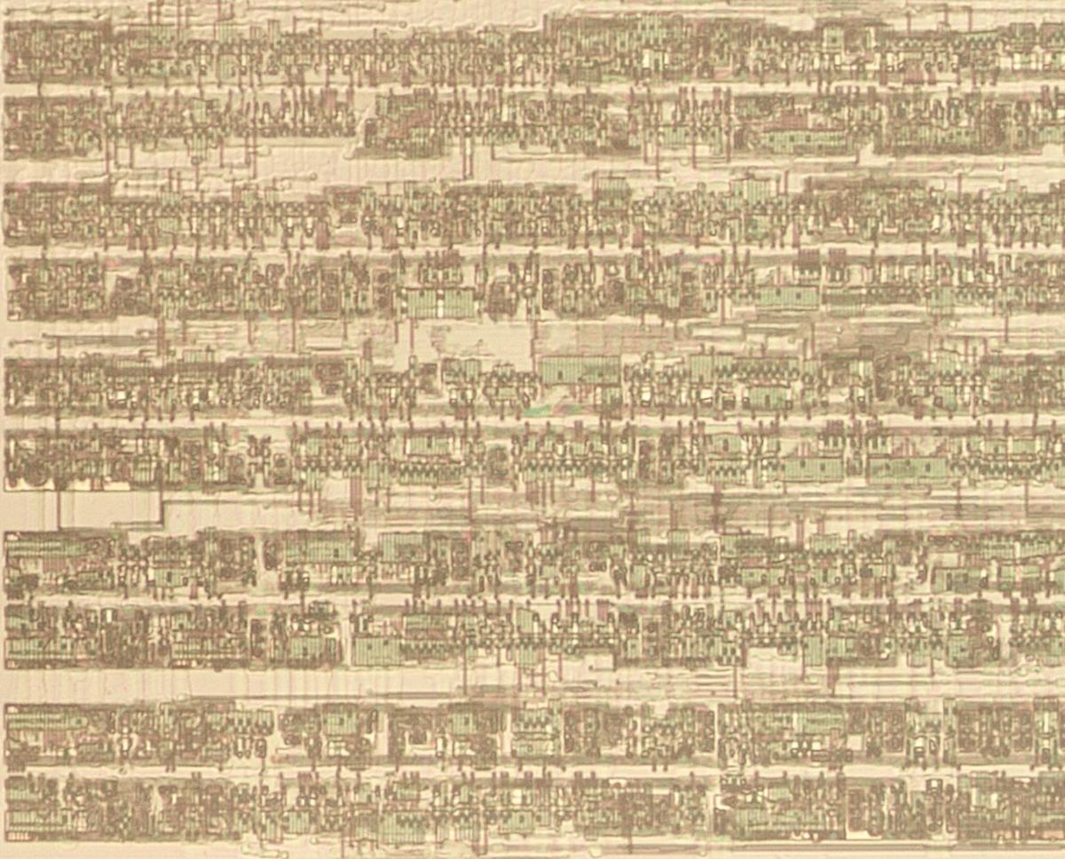
The photo below zooms out to show five rows of standard cells (the dark bands) and the wiring in between. Because CMOS circuitry uses two types of transistors (NMOS and PMOS), each standard-cell row appears as two closely-spaced bands: one of NMOS transistors and one of PMOS transistors. The space between rows is used as a "wiring channel" that holds the wiring between the cells. Power and ground for the circuitry run along the top and bottom of each row.

Some standard cells in the Pentium processor.

Some standard cells in the Pentium processor.

The fixed structure of standard cell design makes it suitable for automation, with the layout generated by "automatic place and route" software. The first step, placement, consists of determining an arrangement of cells that minimizes the distance between connected cells. Running long wires between cells wastes space on the die, since you end up with a lot of unnecessary metal wiring. But more importantly, long paths have higher capacitance, slowing down the signals. Once the cells are placed in their positions, the "routing" step generates the wiring to connect the calls. Placement and routing are both difficult optimization problems that are NP-complete.

Intel started using automated place and route techniques for the 386 processor, since it was much faster than manual layout and dramatically reduced the number of errors. Placement was done with a program called Timberwolf, developed by a Berkeley grad student. As one member of the 386 team said, "If management had known that we were using a tool by some grad student as a key part of the methodology, they would never have let us use it." Intel developed custom software for routing, using an iterative heuristic approach. Standard-cell design is still used in current processors, but the software is much more advanced.

A brief overview of CMOS

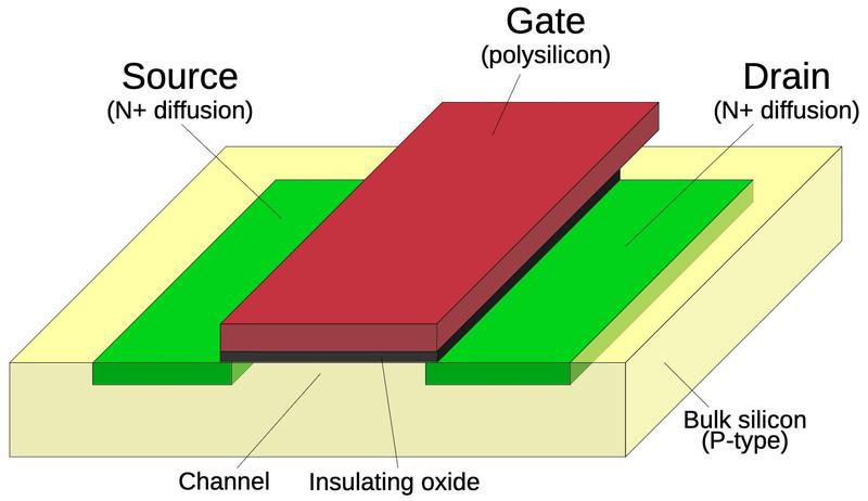
Before looking at the standard cell circuits in detail, I'll give a quick overview of how CMOS circuits are implemented. Modern processors are built from CMOS circuitry, which uses two types of transistors: NMOS and PMOS. The diagram below shows how an NMOS transistor is constructed. The transistor can be considered a switch between the source and drain, controlled by the gate. The source and drain regions (green) consist of silicon doped with impurities to change its semiconductor properties, forming N+ silicon. The gate consists of a layer of polysilicon (red), separated from the silicon by a very thin insulating oxide layer. Whenever polysilicon crosses active silicon, a transistor is formed.

Diagram showing the structure of an NMOS transistor.

Diagram showing the structure of an NMOS transistor.

The NMOS and PMOS transistors are opposite in their construction and operation. A PMOS transistor swaps the N-type and P-type silicon, so it consists of P+ regions in a substrate of N silicon. In operation, an NMOS transistor turns on when the gate is high, while a PMOS transistor turns on when the gate is low.4 An NMOS transistor is best at pulling its output low, while a PMOS transistor is best at pulling its output high. In a CMOS circuit, the transistors work as a team, pulling the output high or low as needed; the "C" in CMOS indicates this "Complementary" approach. NMOS and PMOS transistors are not entirely symmetrical, however, due to the underlying semiconductor physics. Instead, PMOS transistors need to be larger than NMOS transistors, which helps to distinguish PMOS transistors from NMOS transistors on the die.

The layers of circuitry in the Pentium

The construction of the Pentium is more complicated than the diagram above, with four layers of metal wiring that connect the transistors.5 Starting at the surface of the silicon die, the Pentium's transistors are similar to the diagram, with regions of silicon doped to change their semiconductor properties. Polysilicon wiring is created on top of the silicon. The most important role of the polysilicon is that when it crosses doped silicon, a transistor is formed, with the polysilicon as the gate. However, polysilicon is also used as wiring over short distances.

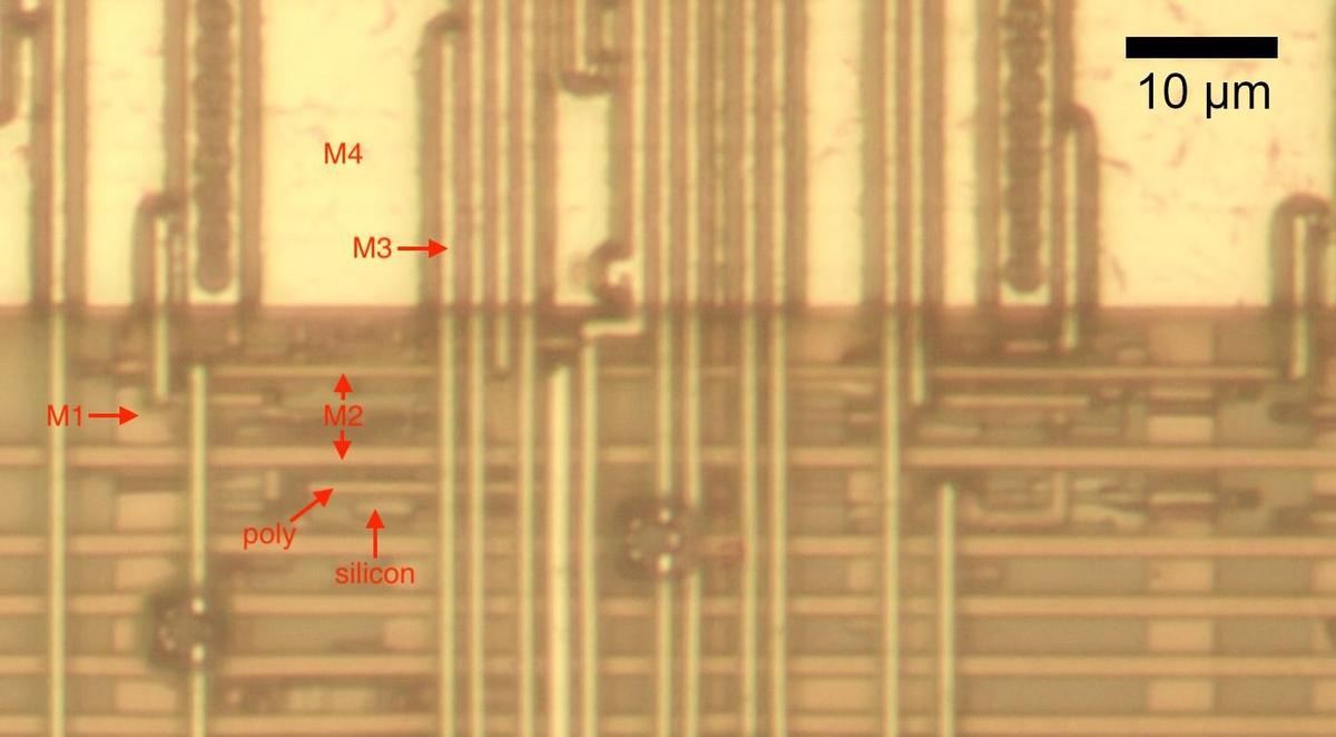
Above the silicon, four layers of metal connect the components: multiple metal layers allow signals to crisscross the chip without running into each other. The metal layers are numbered M1 through M4, with M1 on the bottom. A few rules control the wiring: a metal layer can connect with the layer above or below through a tungsten plug called a "via". Only the bottom metal, M1, can connect to the silicon or polysilicon, through a "contact". The layers usually alternate between horizontal wiring and vertical wiring (at least locally). Thus, a signal from a transistor may travel through M1, bounce up to M2 and M3 to cross other signals, and then go back down to M1 to connect to another transistor. As you can see, automated place and route software has a complicated task, producing millions of complicated wiring paths as densely as possible.
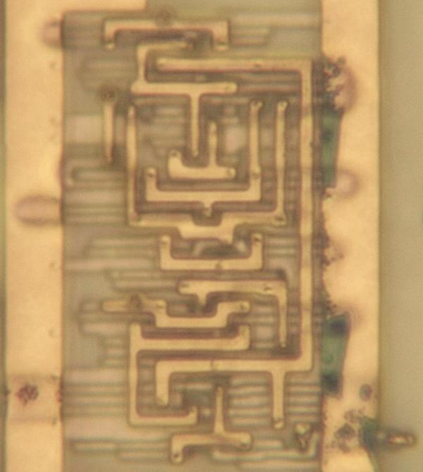
The diagram below shows how the layers appear on the chip. (This photo shows one of the rare spots on the chip where all the layers are visible.) The M4 metal layer on top of the chip is the thickest, so it is mostly used for power, ground, and clock signals rather than data. An M4 ground wire covers the top of this photo. The next layer down is M3. In this part of the chip, M3 lines run vertically. (Due to optical effects, the vertical M3 lines may look like they are on top of M4, but they are below.) The horizontal M2 metal lines are lower and appear brown rather than golden, due to the oxide layers that cover them. The bottom metal layer is M1. The vertical M1 lines are thick in this part of the chip because they provide power to the circuitry.

The Pentium is constructed with four layers of metal. Because the chip has a three-dimensional structure, I used focus stacking to get a clearer image.

The Pentium is constructed with four layers of metal. Because the chip has a three-dimensional structure, I used focus stacking to get a clearer image.

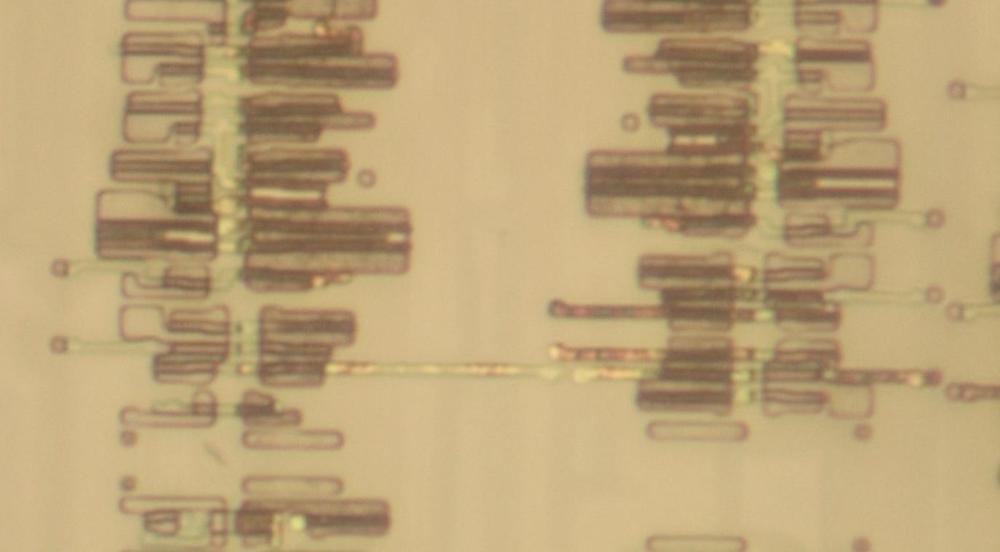
The silicon and polysilicon are mostly obscured in the above photo. By removing all the metal layers, I obtained the image below. This image shows the same region as the image above, but it is hard to see the correlation because the metal layers almost completely obscure the silicon. The orderly columns of transistors reveal the standard-cell design. The irregular dark regions are doped silicon, which forms the chip's transistors. The dark or shiny horizontal bands are polysilicon. I will explain below how these regions form gates and other circuits.

A closeup of the silicon and polysilicon.

A closeup of the silicon and polysilicon.

Inverter

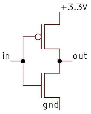
The fundamental CMOS gate is an inverter, shown in the schematic below. The inverter is built from one PMOS transistor (top) and one NMOS transistor (bottom). If the gate input is a "1", the bottom transistor turns on, pulling the output to ground (0). A "0" input turns on the top transistor, pulling the output high (1). Thus, this two-transistor circuit implements an inverter.10

Schematic diagram of a CMOS inverter.

Schematic diagram of a CMOS inverter.

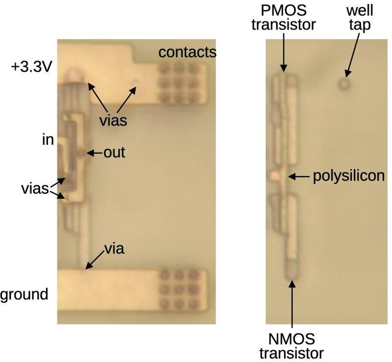
The diagram below shows two views of how a standard-cell inverter appears on the Pentium die, with and without metal. The inverter consists of two transistors, just like the schematic above. The input is connected to the two polysilicon gates of the transistors. The metal output wire is connected to the two transistors (the left sides, specifically).

A standard-cell CMOS inverter in the Pentium.

A standard-cell CMOS inverter in the Pentium.

In more detail, the image on the left includes the bottom (M1) metal layer, but I removed the other metal layers. Two thick metal lines at the top and bottom provide power and ground to the standard cells. The multiple dark circles are contacts between the M1 metal layer and the metal layer on top (M2), providing a path for power and ground that eventually reaches the top (M4) metal layer and then the chip's pins. (The power and ground wires are thick to provide sufficient current to the circuitry while minimizing voltage drops and noise.) The small, lighter circles are vias that connect the M1 metal layer to the underlying silicon or polysilicon. The input to the gate is provided from the M2 metal, which connects to the M1 layer at the indicated contact. The smaller black dots at the top and bottom of this metal strip are vias, connections to the underlying silicon.

For the image on the right, I removed all four metal layers, revealing the polysilicon and doped silicon. Recall that a transistor is constructed from regions of doped silicon with a stripe of polysilicon between the regions, forming the transistor's gate. The diagram shows the two transistors that form the inverter. When combined with the metal wiring, they form the inverter schematic shown earlier. The final feature is the "well tap". The PMOS transistors are constructed in a "well" of N-doped silicon. The well must be kept at a positive voltage, so periodic "taps" connect the well to the +3.3V supply. As mentioned earlier, the PMOS transistor is larger than the NMOS transistor, which allowed me to figure out the transistor types in the photo.

By the way, the chip is built with a 600 nm process, so the width of the polysilicon lines is approximately 600 nm. For comparison, the wavelength of visible light is 400 to 700 nm, with 600 nm corresponding to orange light. This explains why the microscope photos are somewhat fuzzy; the features are the size of the wavelength of light.6

NAND gate

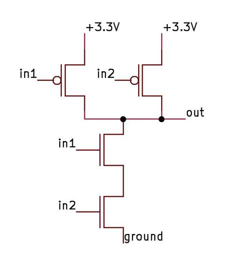
Another common gate in the Pentium is the NAND gate. The schematic below shows a NAND gate with two PMOS transistors above and two NMOS transistors below. If both inputs are high, the two NMOS transistors turn on, pulling the output low. If either input is low, a PMOS transistor turns on, pulling the output high. (Recall that NMOS and PMOS are opposites: a high voltage turns an NMOS transistor on while a low voltage turns a PMOS transistor on.) Thus, the CMOS circuit below produces the desired output for the NAND function.

Schematic of a CMOS NAND gate.

Schematic of a CMOS NAND gate.

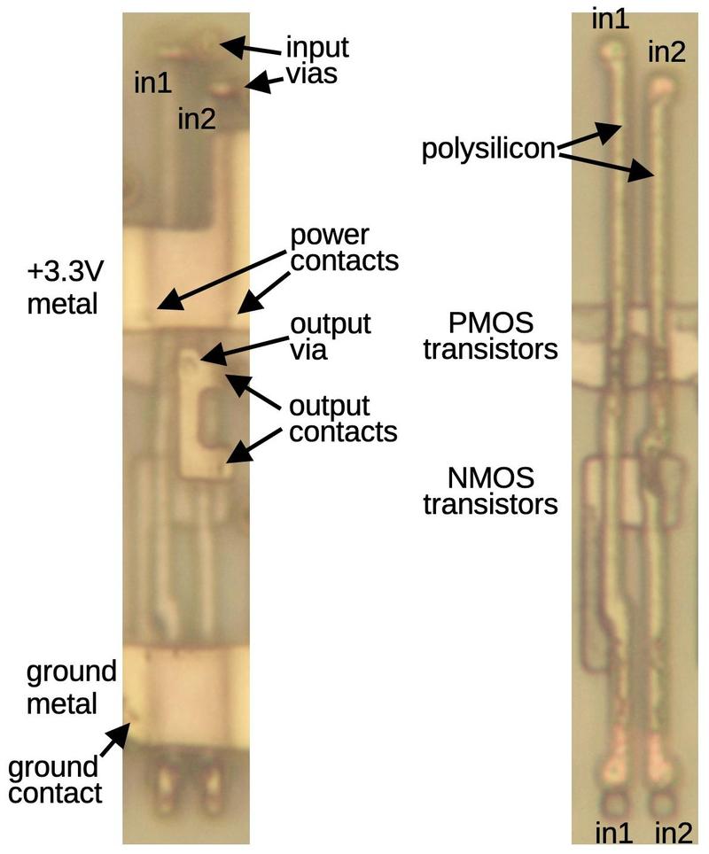
The implementation of the gate as a standard cell, below, follows the schematic. The left photo shows the circuit with one layer of metal (M1). A thick metal line provides 3.3 volts to the gate; it has two contacts that provide power to the two PMOS transistors. The metal line for ground is similar, except only one NMOS transistor is grounded. The thinner metal in the middle has two contacts to get the transistor outputs and a via to connect the output to the M2 metal layer on top. Finally, two tiny bits of M1 metal connect the inputs from the M2 layer to the underlying polysilicon.

Implementation of a CMOS NAND gate as a standard cell.

Implementation of a CMOS NAND gate as a standard cell.

The right photo shows the circuit with all metal removed, showing the polysilicon and silicon. Since a transistor is formed where a polysilicon line crosses doped silicon, the two polysilicon lines create four transistors. Polysilicon functions both as local wiring and as the transistor gates. In particular, the inputs can be connected at the top or bottom of the circuit (or both), depending on what works best for wiring the circuitry. Note that the transistors are squashed together so the silicon in the middle is part of two transistors. An important asymmetry is that the output is taken from the middle of the PMOS transistors, wiring them in parallel, while the output is taken from the right side of the NMOS transistors, wiring them in series.

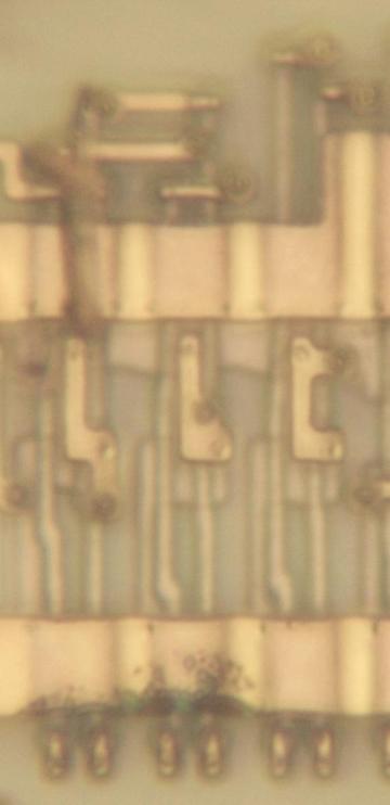
Zooming out a bit, the photo below shows three NAND gates. Although the underlying standard cell is the same for each one, there are differences between the gates. At the top, horizontal wiring links the inputs to M2 through vias. The length of each polysilicon line depends on the position of the metal. Moreover, in the middle of each gate, the metal connection to the output is positioned differently. Finally, note that the power wiring shifts upward in the upper right corner; this is to make room for a larger cell to the right. The point is that the standard cells aren't simply copies of each other, but are adjusted in each case to put the inputs, outputs, and power in the right location. Also note that these standard cells are not isolated, but are squeezed together so the PMOS transistors are touching. This optimization slightly increases the density.

Three NAND gates in the Pentium.

Three NAND gates in the Pentium.

OR-NAND gate

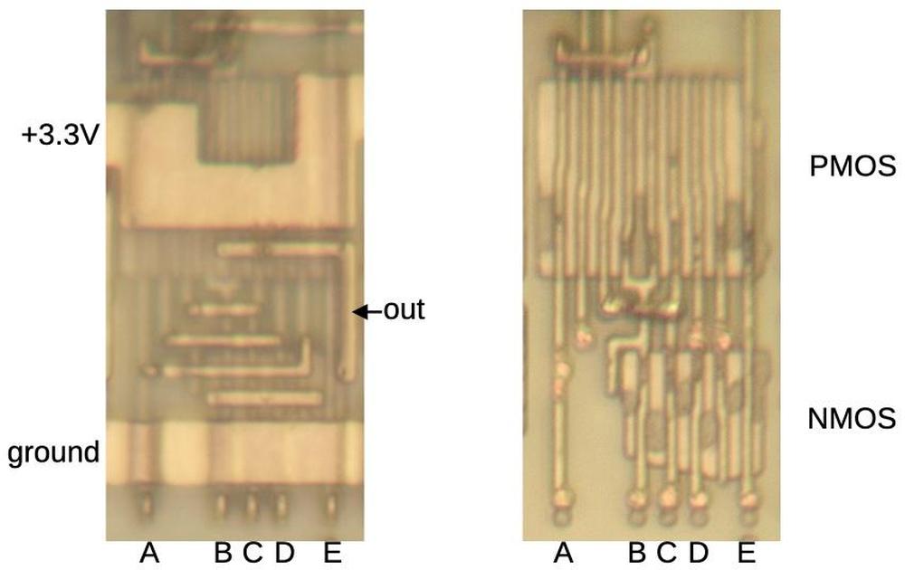
The standard cell library includes some complex gates. For instance, the gate below is a 5-input OR-NAND gate, computing ~((A+B+C+D)⋅E). In the NMOS circuit, transistors A through D are paralleled while E is in series. The PMOS circuit is the opposite, with A through D in series and E in parallel. To provide sufficient current, the PMOS circuit has two sets of transistors for A through D, so the PMOS block is much larger than the NMOS block.

The OR-NAND gate as it appears on the die. The left image shows the M1 metal layer while the right image shows the silicon
and polysilicon.

The OR-NAND gate as it appears on the die. The left image shows the M1 metal layer while the right image shows the silicon and polysilicon.

Latch

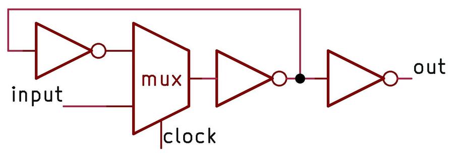
One of the key building blocks of the Pentium's circuitry is the latch. The idea of the latch is to hold one bit, controlled by the clock signal. A latch is "transparent": the latch's input immediately appears on the output while the clock is high. But when the clock is low, the latch holds its previous value. The latch is implemented with a feedback loop that passes the latch's output back into the latch. The heart of this latch circuit is the multiplexer (mux), which selects either the previous output (when the clock is low) or the new input (when the clock is high). The inverters amplify the feedback signal so it doesn't decay in the loop. An inverter also amplifies the output so it can drive other circuitry.

The circuit for a latch.

The circuit for a latch.

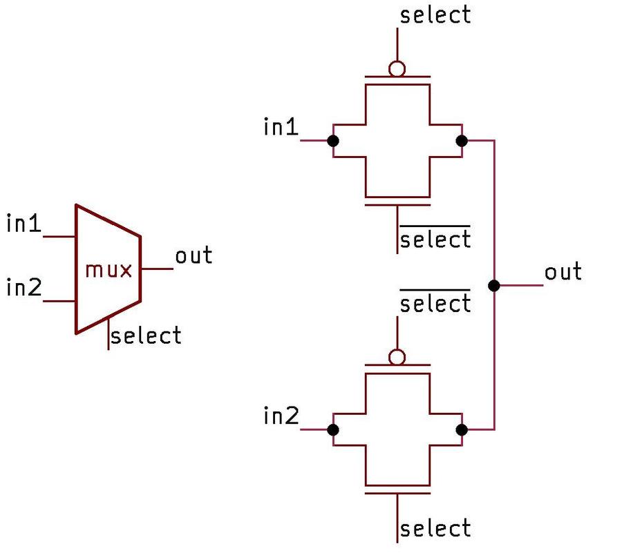
The circuit for a multiplexer is interesting since it uses "pass transistors". That is, the transistors simply pass their input through to the output, rather than pulling a signal to power or ground as in a typical logic gate. The schematic shows how this works. First, suppose that the select line is low. This will turn on the two transistors connected to the first input, allowing its level to flow to the output. Meanwhile, both transistors connected to the second input will be turned off, blocking that signal. But if the select line is high, everything switches. Now, the two transistors connected to the second input turn on, passing its level to the output. Thus, the multiplexer selects the first input if the control signal is low, and the second input if the control signal is high.

A multiplexer and its implementation in CMOS.

A multiplexer and its implementation in CMOS.

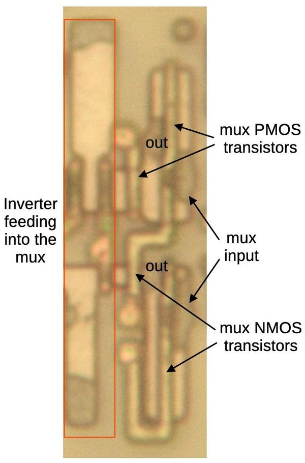
The diagram below shows a multiplexer, part of a latch. On the left, an inverter feeds into one input of the multiplexer.7 On the right is the other input to the multiplexer. The output is taken from the middle, between the pairs of the transistors.

A multiplexer as it appears on the Pentium die.

A multiplexer as it appears on the Pentium die.

Note that the multiplexer's circuit is opposite, in a way, to a logic gate. In a logic gate, you want either the NMOS transistor on or the PMOS transistor on, so the output is pulled low or high respectively. This is accomplished by giving the signals on the transistor gates the same polarity, so the same polysilicon line runs through both transistors. In a multiplexer, however, you want the corresponding PMOS and NMOS transistors to turn on at the same time, so they can pass the signal. This requires the signals on the transistor gates to have opposite polarity. One polysilicon line runs through the right PMOS transistor and the left NMOS transistor. The other polysilicon line runs through the left PMOS transistor and the right NMOS transistor, connected by metal wiring (not shown). The multiplexer includes an inverter to provide the necessary signal, but I cropped it out of the diagram below.

The flip-flop

The Pentium makes extensive use of flip-flops. A flip-flop is similar to a latch, except its clock input is edge-sensitive instead of level-sensitive. That is, the flip-flop "remembers" its input at the moment the clock goes from low to high, and provides that value as its output. This difference may seem unimportant, but it turns out to make the flip-flop more useful in counters, state machines, and other clocked circuits.

In the Pentium, a flip-flop is constructed from two latches: a primary latch and a secondary latch. The primary latch passes its value through while the clock is low and holds its value when the clock is high. The output of the primary latch is fed into the secondary latch, which has the opposite clock behavior. The result is that when the clock switches from low to high, the primary latch stops updating its output at the same time that the secondary starts passing this value through, providing the desired flip-flop behavior.

A standard-cell flip-flop.

A standard-cell flip-flop.

The photo above shows a standard-cell flop-flop, with an intricate pattern of metal wiring connecting the various sub-components. There are a few variants; with minor logic changes, the flip-flop can have "set" or "reset" inputs, bypassing the clock to force the output to the desired state. (Set and reset functions are useful for initializing flip-flops to a desired value, for example when the processor starts up.)

The BiCMOS buffer

Although I've been discussing CMOS circuits so far, the Pentium was built with BiCMOS, a process that allows circuits to use bipolar transistors in addition to CMOS. By adding a few extra processing steps to the regular CMOS manufacturing process, bipolar (NPN and PNP) transistors can be created. The Pentium made extensive use of BiCMOS circuits since they reduced signal delays by up to 35%. Intel also used BiCMOS for the Pentium Pro, Pentium II, Pentium III, and Xeon processors (but not the Pentium MMX). However, as chip voltages dropped, the benefit from bipolar transistors dropped too and BiCMOS was eventually abandoned.

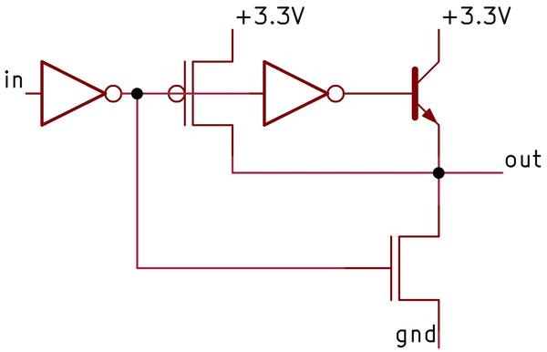
The schematic below shows a standard-cell BiCMOS buffer in the Pentium chip.8 This circuit is more complex than a CMOS buffer: it uses two inverters, an NPN pull-up transistor, an NMOS pull-down transistor, and a PMOS pull-up transistor.9

Reverse-engineered schematic of the BiCMOS buffer.

Reverse-engineered schematic of the BiCMOS buffer.

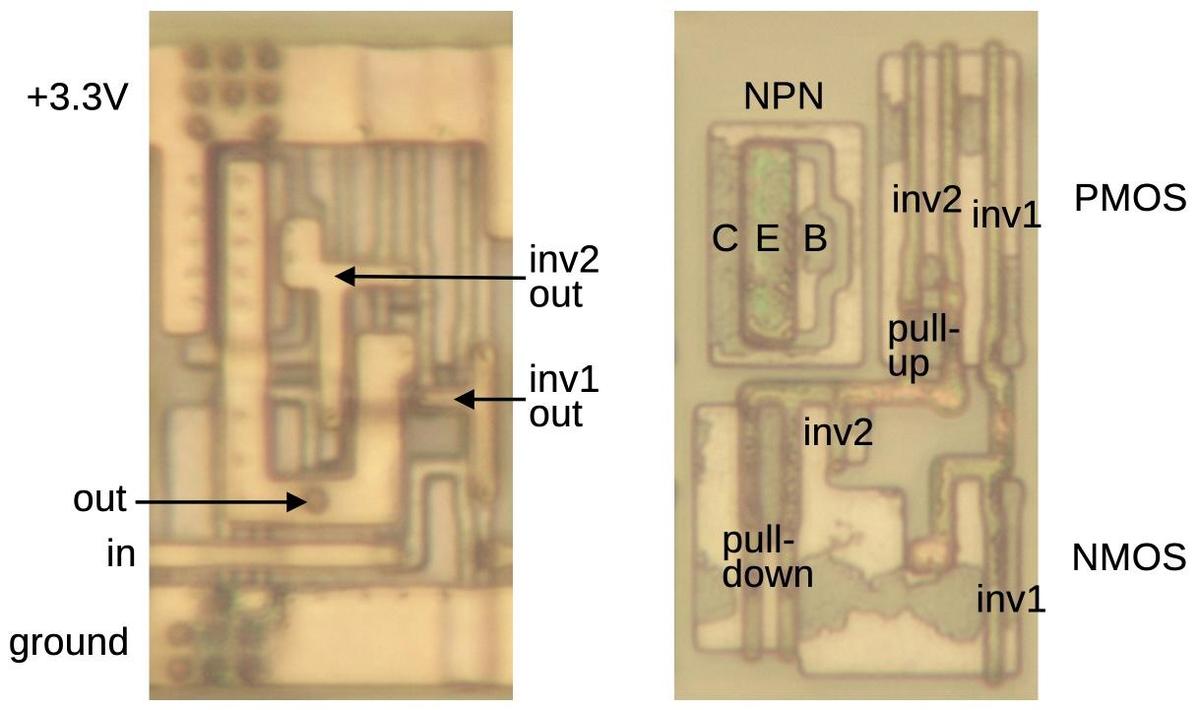
In the die images below, note the circular structure of the NPN transistor, very different from the linear structure of the NMOS and PMOS transistors and considerably larger. A sign of the buffer's high-current drive capacity is the output's thick metal wiring, much thicker than the typical signal wiring.

A BiCMOS buffer in the Pentium.

A BiCMOS buffer in the Pentium.

Conclusions

Standard-cell layout is extensively used in modern chips. Modern processors, with their nanometer-scale transistors, are much too small to study under a microscope. The Pentium, on the other hand, has features large enough that its circuits can be observed and reverse engineered. Of course, with 3.3 million transistors, the Pentium is too much for me to reverse engineer in depth, but I still find it interesting to study small-scale circuits and see how they were implemented. This post presented a small sample of the standard cells in the Pentium. The full standard-cell library is much larger, with dozens, if not hundreds, of different cells: many types of logic gates in a variety of sizes and drive strengths. But the fundamental design and layout principles are the same as the cells described here.

One unusual feature of the Pentium is its use of BiCMOS circuitry, which had a peak of popularity in the 1990s, right around the era of the Pentium. Although changing tradeoffs made BiCMOS impractical for digital circuitry, BiCMOS still has an important role in analog ICs, especially high-frequency applications. The Pentium in a sense is a time capsule with its use of BiCMOS.

I hope that you have enjoyed this look at some of the Pentium's circuits. I find it reassuring to see that even complex processors are made up of simple transistor circuits and you can observe and understand these circuits if you look closely.

For more on standard-cell circuits, I wrote about standard cells in an IBM chip and standard cells in the 386 (the 386 article has a lot of overlap with this one). Follow me on Twitter @kenshirriff or RSS for updates. I'm also on Mastodon occasionally as @[email protected].

Notes and references

  1. In this blog post, I'm focusing on the "P54C" version of the original Pentium processor. Intel produced many different versions of the Pentium, and it can be hard to keep them straight. Part of the problem is that "Pentium" is a brand name, with multiple microarchitectures, lines, and products. At the high level, the Pentium (1993) was followed by the Pentium Pro (1995) Pentium II (1997), Pentium III (1999), Pentium 4 (2000), and so on. The original Pentium used the P5 microarchitecture, a superscalar microarchitecture that was advanced but still executed instruction in order like traditional microprocessors. The Pentium Pro was a major jump, implementing a microarchitecture called P6 that broke instructions into micro-operations and executed them out of order using dataflow techniques. The next microarchitecture version was NetBurst, first used with the Pentium 4. NetBurst provided a deep pipeline and introduced hyper-threading, but it was disappointingly slow and was replaced by the Core microarchitecture. The Core microarchitecture is based on the P6 and is Intel's current microarchitecture.

    I'll focus now on the original Pentium, which went through several substantial revisions. The first Pentium product was the 80501 (codenamed P5), running at 60 or 66 MHz and using 5 volts. These chips were built with an 800 nm process and contained 3.1 million transistors.

    The power consumption of these chips was disappointing, so Intel improved the chip, producing the 80502. These chips, codenamed P54C, used 3.3 volts and ran at 75-120 MHz. The chip's architecture remained essentially the same but support was added for multiprocessing, boosting the transistor count to 3.3 million. The P54C had a much more advanced clock circuit, allowing the external bus speed to stay low (50-66 MHz) while the internal clock speed—and thus performance—climbed to 100 MHz. The chips were built with a smaller 600 nm process with four layers of metal, compared to the previous three. Visually, the die of the P54C is almost the same as the P5, with the additional multiprocessing logic at the bottom and the clock circuitry at the top. For this article, I examined the P54C, but the standard cells should be similar in other versions.

    Next, Intel moved to the 350 nm process, producing a smaller, faster Pentium chip, codenamed the P54CS; the die looks almost identical to the P54C (but smaller), with subtle changes to the bond pads. Another variant was designed for mobile use: the Pentium processor with "Voltage Reduction Technology" reduced power consumption by using a 2.9- or 3.1-volt supply for the core and a 3.3-volt supply to drive the I/O pins. These were built first with the 600 nm process (75-100 MHz) and then the 350 nm process (100-150 MHz).

    The biggest change to the original Pentium was the Pentium MMX, with part number 80503 and codename P55C. This chip extended the x86 instruction set with 57 new instructions for vector processing. It was built on a 350 nm process before moving to 280 nm, and had 4.5 million transistors. More obscure variants of the original Pentium include the P54CQS, P54CS, P54LM, P24T, and Tillamook, but I won't get into them. 

  2. Circuits that had a high degree of regularity, such as the arithmetic/logic unit (ALU) or register storage were typically constructed by manually laying out a block to implement the circuitry for one bit and then repeating the block as needed. Because a circuit was repeated 32 times for the 32-bit processor, the additional effort was worthwhile. 

  3. An alternative layout technique is the gate array, which doesn't provide as much flexibility as a standard cell approach. In a gate array (sometimes called a master slice), the chip had a fixed array of transistors (and often resistors). The chip could be customized for a particular application by designing the metal layer to connect the transistors as needed. The density of the chip was usually poor, but gate arrays were much faster to design, so they were advantageous for applications that didn't need high density or produced a relatively small volume of chips. Moreover, manufacturing was much faster because the silicon wafers could be constructed in advance with the transistor array and warehoused. Putting the metal layer on top for a particular application could then be quick. Similar gate arrays used a fixed arrangement of logic gates or flip-flops, rather than transistors. Gate arrays date back to 1967

  4. The behavior of MOS transistors is complicated, so the description above is simplified, just enough to understand digital circuits. In particular, MOS transistors don't simply switch between "on" and "off" but have states in between. This allows MOS transistors to be used in a wide variety of analog circuits. 

  5. The earliest Pentiums had three layers of metal wiring, but Intel moved to a four-layer process with the P54C die, the version that I'm examining. 

  6. To get this level of magnification with my microscope, I had to use an oil immersion lens. Instead of looking at the chip in air, as with a normal lens, I had to put a drop of special microscope oil on the chip. I carefully lower the lens until it dips into the oil (making sure I don't crash the lens into the chip). The purpose of the oil is that its index of refraction is almost the same as glass, much higher than air. This gives the lens a higher "numerical aperture", allowing the lens to resolve smaller details. 

  7. For completeness, I'll mention that the inverter feeding the multiplexer inverter isn't exactly an inverter. Specifically, the inverter's two transistors are not tied together to produce an output. Instead, the inverter's NMOS transistor provides an input to the multiplexer's NMOS transistor and likewise, the PMOS transistor provides an input to the PMOS transistor. The omission of this connection does not affect the circuit's behavior, but it makes calling the circuit an inverter and a multiplexer a bit of an abstraction. 

  8. Intel called this gate "BiNMOS" rather than "BiCMOS" because it uses a bipolar transistor and an NMOS transistor to drive the output, rather than two bipolar transistors. The Pentium's BiCMOS circuitry is described in a conference paper, showing a second NPN transistor to protect the first one. I don't see the second transistor on the die so the two transistors may be implemented in one silicon structure. Reference: R. F. Krick et al., “A 150 MHz 0.6 µm BiCMOS superscalar microprocessor,” IEEE Journal of Solid-State Circuits, vol. 29, no. 12, Dec. 1994, doi:10.1109/4.340418

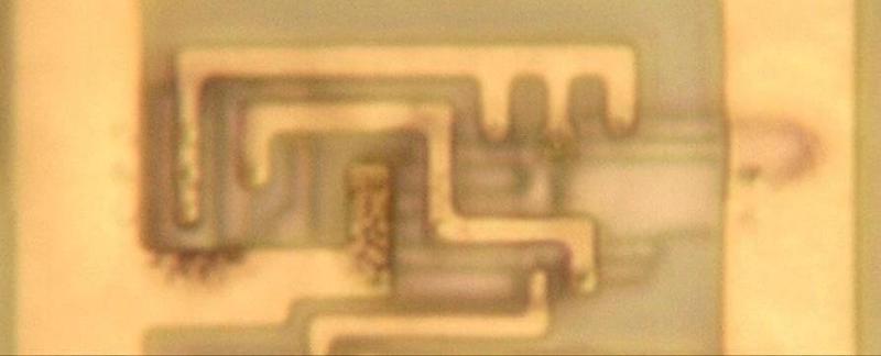
  9. The Pentium contains multiple types of BiCMOS standard cells, which I'll show in this footnote. The cell below is an inverter. It is similar to the BiCMOS buffer described earlier, except it lacks the first inverter in the circuit. To make room for the NPN transistor on the left, the PMOS transistors are shifted to the right. As a result, they don't line up with the PMOS transistors in other cells. This is a break from the traditional orderliness of standard cells.

    A BiCMOS inverter with PMOS on the left and NMOS on the right. The input is at the bottom and the output is in the middle.

    A BiCMOS inverter with PMOS on the left and NMOS on the right. The input is at the bottom and the output is in the middle.

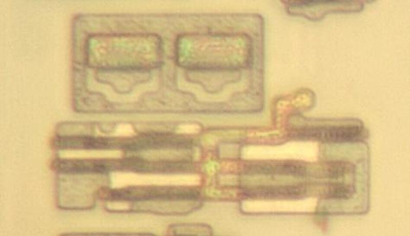
    The BiCMOS inverter below is similar, except it uses two NPN transistors, providing more output drive. I removed the M1 metal layer to provide a better view of the transistors.

    A BiCMOS inverter with two NPN transistors. The PMOS transistors are in the lower left and the NMOS transistors are in the lower right.

    A BiCMOS inverter with two NPN transistors. The PMOS transistors are in the lower left and the NMOS transistors are in the lower right.

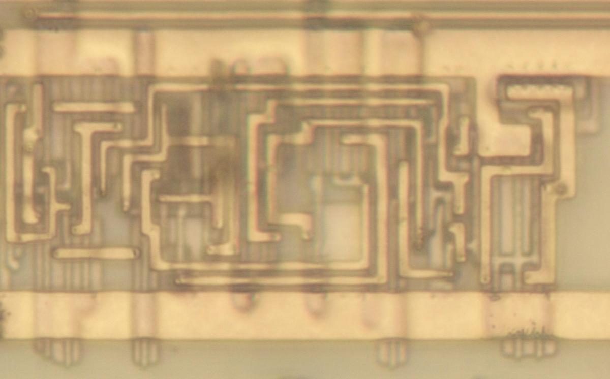
    Another interesting BiCMOS circuit is the D flip-flop with enable and BiCMOS output, shown below. This is similar to the earlier flip-flop except it has an enable input, allowing it to either load a new value triggered by the clock, or to hold its earlier value. This allows the flip-flop to remember a value for more than one clock cycle. The additional functionality is implemented by another multiplexer, selecting either the old value or the new value. (This multiplexer is, in a way, one level higher than the multiplexer in each latch.) The transistor for the BiCMOS output is in the upper right, poking out from under the metal. (This circuit might be implemented as two independent cells, one for the flip-flop and one for the driver; I'm not sure.)

    A D flip-flop in the Pentium.

    A D flip-flop in the Pentium.


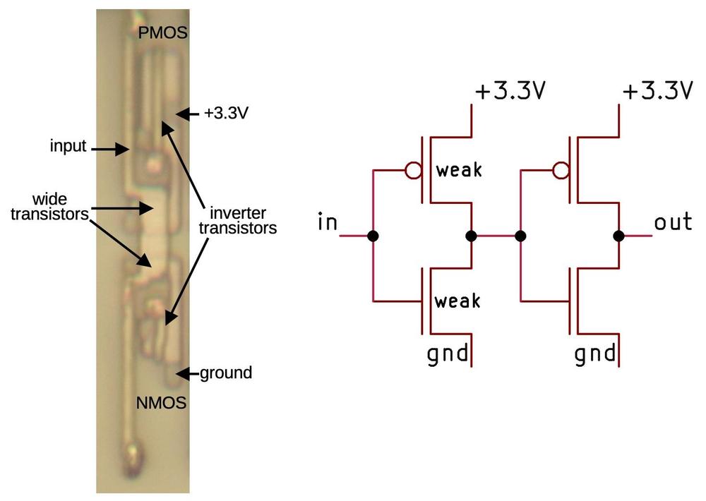
  10. One puzzling inverter variant is used in a gate I'll call the "slow buffer". This buffer consists of two inverters, so it passes its input through to the output, buffered. The strange part is that the first inverter uses transistors with wide gates, which makes these transistors much weaker than regular transistors. As a result, the first inverter will be slow to switch states. My guess is that this circuit is used to delay signals, for example, to keep a signal aligned with another signal that is delayed by multiple logic gates.

    The buffer consists of two inverters. The first inverter uses wide, weak transistors.

    The buffer consists of two inverters. The first inverter uses wide, weak transistors.

    You might expect that larger transistors would be stronger, not weaker. The problem is that these transistors are larger in the wrong dimension. If you make the gate wider, the effect is similar to multiple transistors in parallel, providing more current. But if you make the gate longer (as in this case), the effect is similar to multiple transistors in series, so the resistances add and the total current is reduced. In most cases, transistors are constructed with the smallest gate length possible, which is determined by the manufacturing process, so the transistors here are unusual. This chip was manufactured with an 800 nm process, so the smallest gate length is approximately 800 nm. The gate width (the normal direction for variation) varies dramatically depending on the circuit, optimized to provide maximum performance.