Inside a vintage aerospace navigation computer of uncertain purpose

I recently obtained an aerospace computer from the early 1970s, apparently part of a navigation system. Aerospace computers are an interesting but mostly neglected area of computer hardware, so I'm always delighted to examine one up close. In an era when most computers were large mainframes, aerospace computers packed dense electronics into a small package, using technologies such as surface-mounted components and multi-layer printed circuit boards, technologies that wouldn't reach the mainstream for another decade. This blog post examines the circuitry and components inside this computer, including an unusual electromechanical display. Although I was unable to determine who manufactured this system or even its exact function, this system illustrates how hundreds of integrated circuits and a core memory stack can be crammed into a compact package.

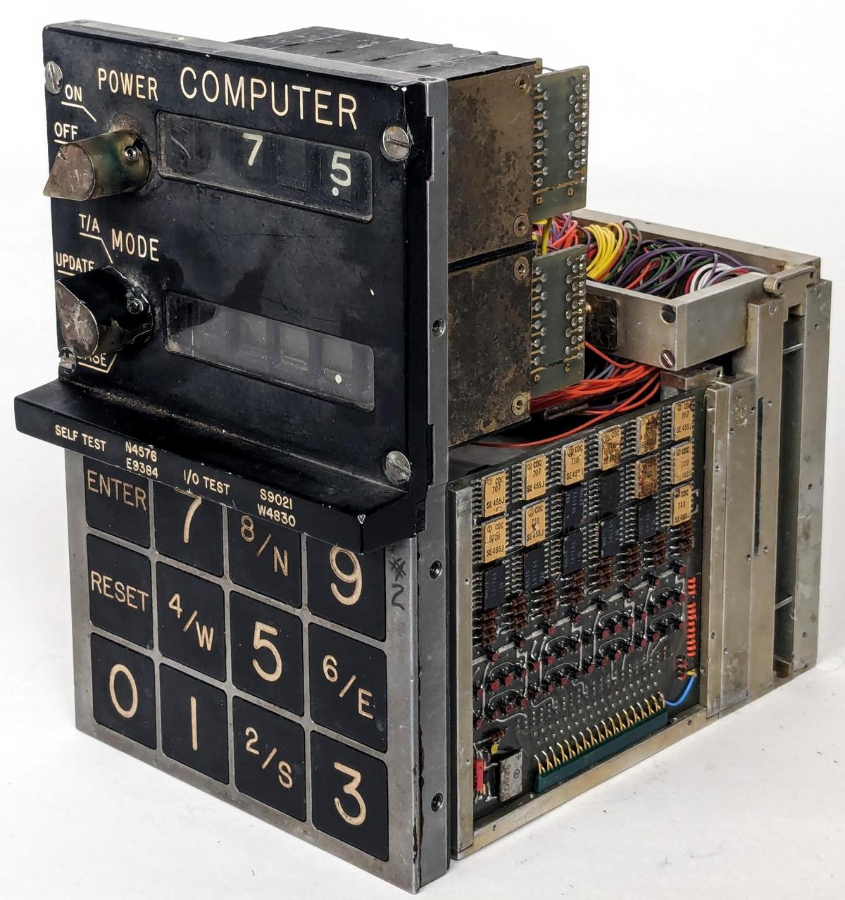
The navigation computer, showing the front panel with the display and keyboard, with the electronics unit behind it. Click this image (or any other) for a larger version.

The navigation computer, showing the front panel with the display and keyboard, with the electronics unit behind it. Click this image (or any other) for a larger version.

The keyboard

The device has a simple numeric keyboard with a few unexpected features. The numeric keypad can also be used for direction entry, as four of the keys have N, S, E, and W on them. The keys are large, roughly the size of the Apollo spacecraft's DSKY buttons. My theory is that these buttons are designed for operation with gloves, perhaps in a fighter plane where the pilot wears a pressure suit. The buttons are hinged at the top, so they don't push straight in, but pivot when pressed.

Numeric keypads typically use one of two layouts: a telephone-style keypad has the digits 123 at the top, while a calculator-style keypad has the digits 789 at the top. Interestingly, this device uses a calculator layout, while most aviation devices have a telephone layout. The Apollo DSKY also used a calculator layout, which could be a hint at a NASA connection for this device.

Above the keyboard are four codes for self-test: N4576, E9384, S9021, and W4830. Entering these codes on the keyboard presumably triggered the appropriate test of the system when the switch is in test mode.

The display

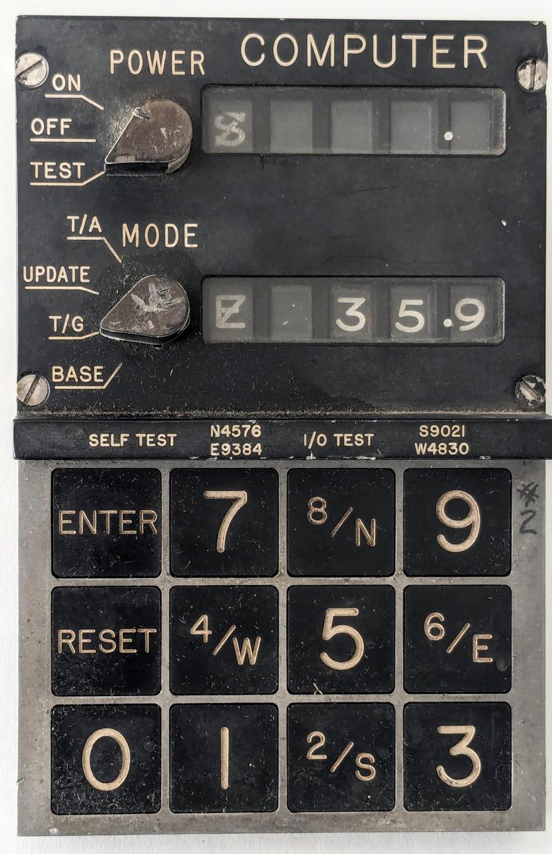
The computer's display is simple, showing a latitude and longitude. Each value has one decimal position, providing 0.1° of accuracy. The latitude and longitude are prefixed with a compass direction: North/South for latitude and East/West for longitude.

The front panel of the navigation computer, with a display and keyboard.

The front panel of the navigation computer, with a display and keyboard.

The display is constructed from an unusual type of electromechanical indicator, with an indicator module for each digit. Each digit position has a rotating wheel with 11 positions (ten digits and a blank). When the indicator module for a position is energized, the wheel spins to the specified position, showing the selected digit. The two leftmost indicators are slightly different as they show a compass direction instead of a digit: N, S, E, or W. Moreover, the direction indicators can also show the compass direction with a diagonal slash through it, as seen above. Perhaps the slashed direction indicates a problem with the value.

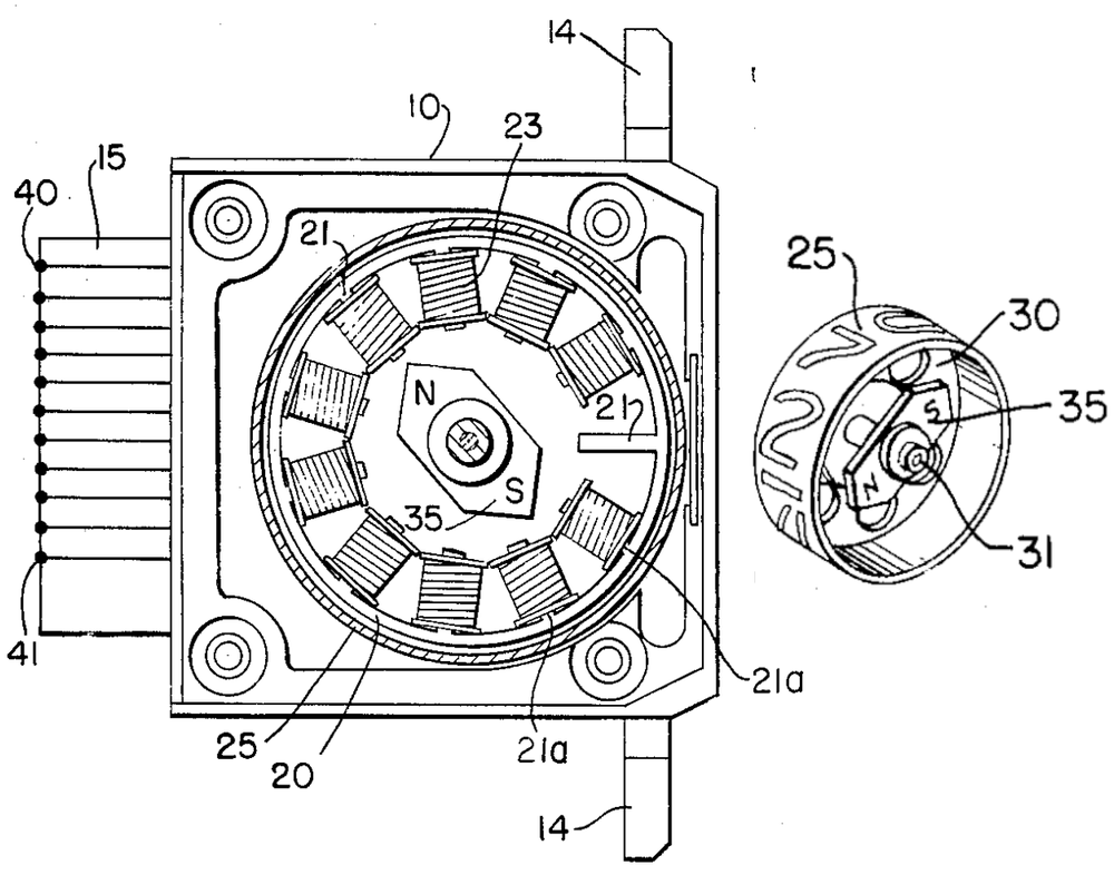
The diagram below shows how a digit indicator operates. Each digit position has an electromagnet with a wire to energize it. The dial wheel has an attached permanent magnet (indicated by N and S). Energizing one of the electromagnets causes the dial to spin to that position, aligning the permanent magnet on the dial with the electromagnet. This mechanism forms a reliable indicator with just one moving part. The displayed digit is clearer than a seven-segment display since the digit uses a real font rather than being created from segments.

A diagram illustrating the magnetic indicator construction. From Patent 3201785. The patent describes a different indicator but the construction is similar.

A diagram illustrating the magnetic indicator construction. From Patent 3201785. The patent describes a different indicator but the construction is similar.

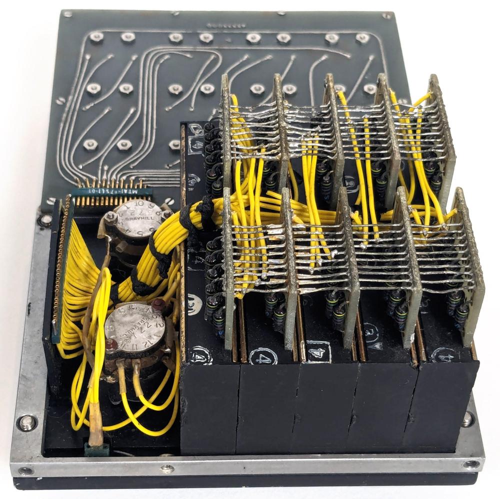
Looking at the back of the keyboard/display unit shows the wiring of the display indicators. Each indicator has a common connection and ten wires to energize one of the electromagnets.1 The electromagnets are connected in a matrix, with all the "1" wires connected, the "2" wires connected, and so forth. To rotate an indicator to a particular digit, a common wire and an electromagnet wire are energized. For instance, powering the common wire of the second indicator and the "5" electromagnetic wire causes the second indicator to rotate to the "5" position. The wiring has a three-dimensional structure with ten bare wires running between the boards, one for each digit value. A yellow wire hangs off each bare wire, linking it to the connector on the left. Each indicator has ten diodes on a circuit board to block "sneak" paths that would energize unselected electromagnets.

The back of the keyboard/display unit. The keyboard buttons are at the back of this photo, while the display modules are at the front.

The back of the keyboard/display unit. The keyboard buttons are at the back of this photo, while the display modules are at the front.

This matrix circuit reduces the amount of wiring required: although there are 100 electromagnets in total, just 20 wires are sufficient to control them. The driver circuitry, however, is a bit more complex as it must scan through the ten digit positions, activating the right pair of driver wires at the right time. Some of the logic circuitry described below must implement this scanning, as well as the driver circuitry to energize the indicators.

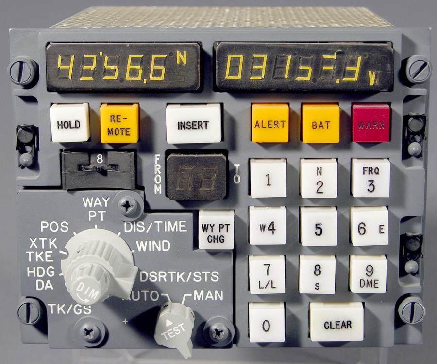
The display and keyboard have many similarities to the Delco Carousel Inertial Navigation System (INS) shown below. (The Delco Carousel was used in many military and civilian aircraft, from the C-141 cargo plane to the Boeing 747 passenger plane.) Both devices have two digital displays, one for latitude North/South and one for longitude East/West. Also note the numeric keypads with four keys assigned to the four compass directions. The controls of the Carousel INS system are considerably more complicated, though. The Carousel has a knob position "TK/GS" (track/ground speed), which may correspond to the "T/G" position on my device.

Control unit for the Delco Carousel inertial navigation system. From Smithsonian collection, gift of Delphi Electronics & Safety.

Control unit for the Delco Carousel inertial navigation system. From Smithsonian collection, gift of Delphi Electronics & Safety.

Note that the display on my unit has just four digits of accuracy, with one digit after the decimal point. A tenth of a degree would provide an accuracy of about ±7 miles, which is low for a navigation device. In comparison, the Delco Carousel has six digits of accuracy (± 100 feet perhaps). This suggests that the device does not provide INS navigation, but some other guidance with lower accuracy.

Packaging the electronics

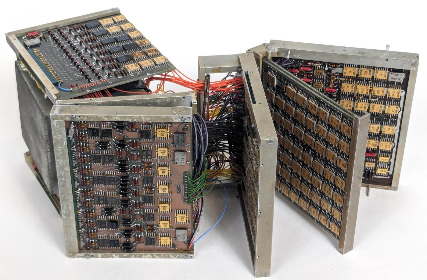
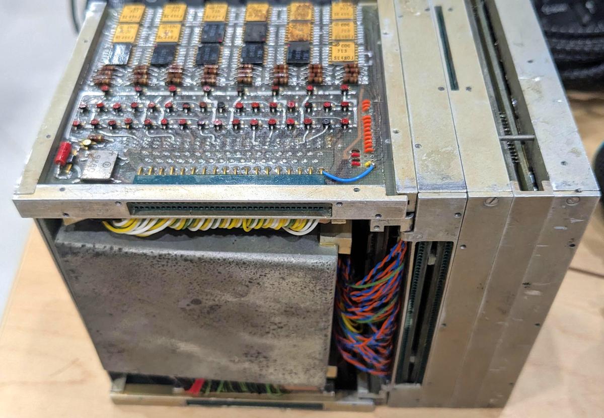
The unit contains 14 circuit boards, crammed with TTL integrated circuits, along with a core memory stack. The photo below shows how circuit boards surround the core memory stack. The mechanical design of the unit is advanced, allowing the boards to be opened up like a book. This provides compact packaging while allowing access to the boards.

The electronics unit can be disassembled and folds open like a book.

The electronics unit can be disassembled and folds open like a book.

The circuit boards are four-layer printed circuit boards, more advanced than the common two-layer boards of the time. The boards use a mixture of surface-mounted and through-hole components. The flat-pack ICs and the tiny round transistors are surface mounted, which was rare at the time. On the other hand, the resistors, capacitors, diodes, and larger transistors use standard through-hole components. At the time, most electronics used through-hole components, although aerospace systems often used surface-mounted components for higher density. It wasn't until the late 1980s that surface-mount technology became commonplace.

The boards are mounted in solid metal frames, providing both structural integrity and heat conduction for cooling. Most of the frames hold two boards, mounted back-to-back for higher density.

The logic boards

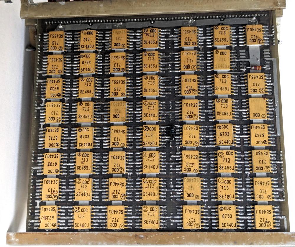
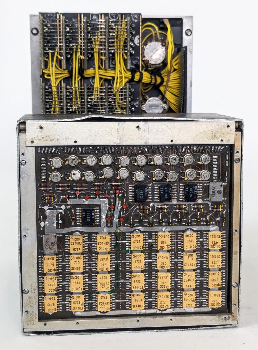
Four of the circuit boards are logic boards, packed with flat-pack integrated circuits. The board below holds 55 integrated circuits, showing the high density that is possible with flat packs.

A board filled with flat-pack logic ICs.

A board filled with flat-pack logic ICs.

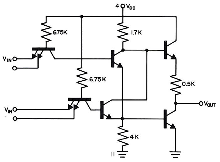
The logic ICs are Signetics 400-series chips, an early type of TTL (Transistor-Transistor Logic) chip. Just three types of these ICs are used: SE440J "Dual exclusive OR" (really AND-OR-INVERT but XOR if provided with particular inputs), SE455J "Dual 4-input buffer/driver" (4-input NAND or NOR gates depending on polarity), and SE480J "Quad 2-input NAND/NOR". These integrated circuits cost $15.45 each in 1966 (about $150 each in current dollars).2

The schematic below shows the circuit that implements AND-OR-INVERT (or exclusive or) in the SE440J. The multiple-emitter transistors on the inputs may appear unusual, but this is the standard way to implement TTL gates. It is important to note that this chip only contains 12 transistors, so the density is low. (Since the chip contains two of these gates, this circuit is duplicated.) In the mid-1960s, integrated circuits only contained a few transistors—the Apollo Guidance Computer's ICs had just 6 transistors—but by the time this unit was built in the early 1970s, some chips had thousands of transistors, tracking Moore's Law. Thus, this unit both illustrates how aviation computers could be built from simple integrated circuits and how the dramatic improvements in IC technology rapidly obsoleted these computers.

Schematic of the SE440J integrated circuit. From datasheet.

Schematic of the SE440J integrated circuit. From datasheet.

The Signetics 400-series seems to have been obscure and short-lived, probably killed off by the wild success of 7400-series TTL chips. I was able to find only a few announcements and datasheets for these chips. The only users of these chips that I could find were NASA projects from the late 1960s.3 Signetics 400-series chips were used in the Mariner Mars and Venus probes, in the Data Automation Subsystem (DAS) (link, link). The Voyager Mars probes also used them. The SE455J gates were also used to interface the Apollo Guidance Computer to a core-rope simulator. JPL used the SE455J in a core memory system. NASA used the SE455J, SE480J, and other Signetics chips in its design for the MICROMIN computer. None of these systems appear to be related to the navigation system, but they illustrate that NASA was using these specific Signetics chips at the time in multiple designs.

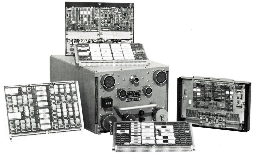
The chips are labeled "CDC", raising the possibility that these chips were built by Control Data Corporation (CDC) under license from Signetics. The Aerospace Division of CDC was active at the time, building various compact computer systems. For instance, the CDC 480 computer (1976) was a 16-bit computer based on the Am2900 bit-slice chip. Also known as the AN/AYK-14, this system was used on numerous aircraft including the F-18. An earlier CDC aerospace computer is the AN/AWG-9 Airborne Missile Control System (1965), a 24-bit computer in a compact 1.1 cubic foot package. Used on the F-14 fighter plane, this computer guided the Phoenix air-to-air missile. Based on CDC's activity in aerospace computers at the time, the mystery computer could be a CDC system, although this hypothesis is based solely on integrated circuits labeled "CDC".

The CDC AN/AYK-14 computer with circuit boards. This is an example of an aerospace computer built by CDC slightly later than the mystery computer. From a 1983 brochure.

The CDC AN/AYK-14 computer with circuit boards. This is an example of an aerospace computer built by CDC slightly later than the mystery computer. From a 1983 brochure.

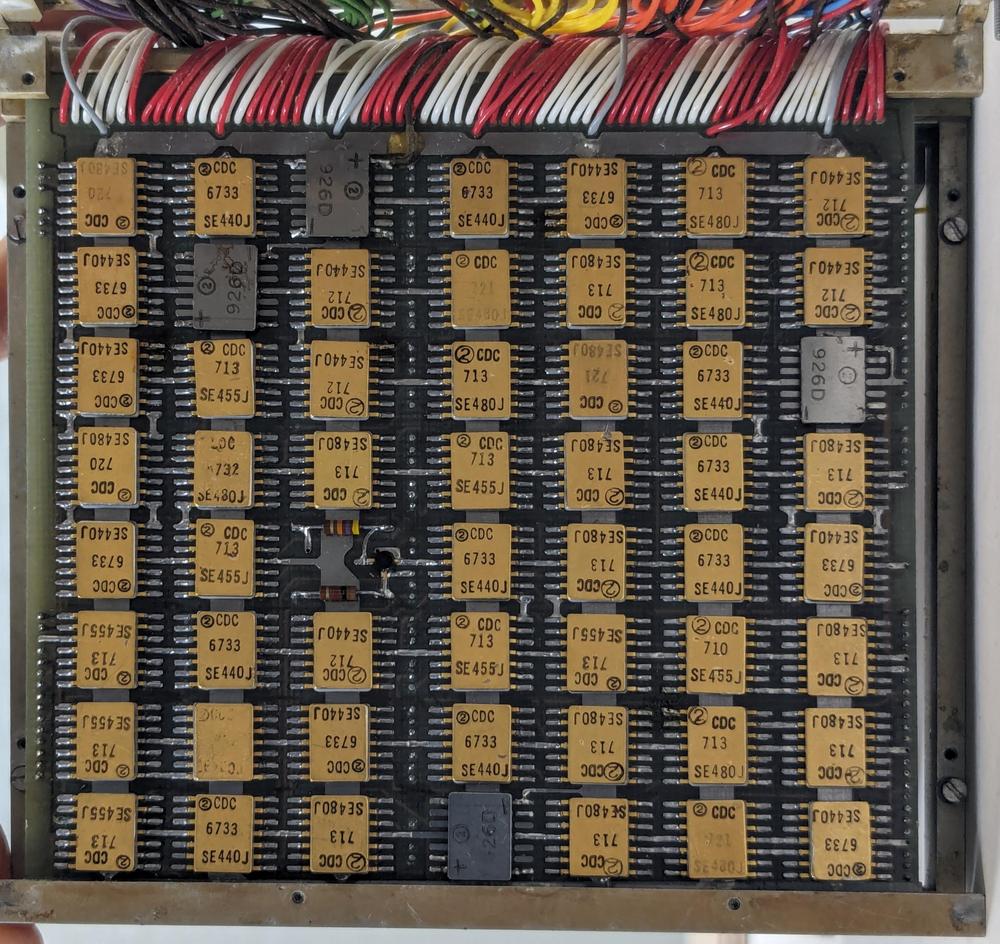
The photo below shows another logic board. This one has numerous red and white wires attached, linking it to the rest of the system. Curiously, this board has a single transistor, with two associated resistors, in the middle of the board.

Another logic board, with a similar grid of flat-pack integrated circuits.

Another logic board, with a similar grid of flat-pack integrated circuits.

Analog boards

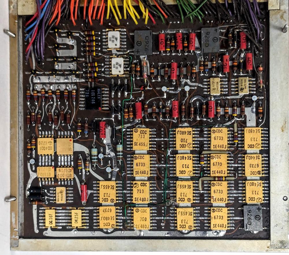
The computer contains not only logic boards but also boards full of analog circuitry to interface with the core memory, keyboard, and display. The board below contains 17 of the logic ICs seen earlier. However, it also uses many resistors, capacitors (red cylinders), transistors (white circles), inductors (white banded cylinders), and glass diodes. The board also has some analog integrated circuits. In particular, it has three TI SN52709 op-amps, the smaller 10-pin packages. The board also contains some integrated circuits that I couldn't identify: UT1000, UT1027, UD4001, and D245F. The SM 60 ICs in white packages have a logo that I don't recognize. The op-amps could function as sense amplifiers for the core memory, or this board could provide other analog interfacing.

A board with some analog integrated circuits.

A board with some analog integrated circuits.

The board has multiple gray four-pin packages labeled "926D". Based on the + and - markings, these packages are probably bridge rectifiers, maybe providing power for the circuits. Many of the other boards have these rectifiers. The analog boards also contain a few Halex flat-pack devices labeled "HALEX 101205 727". Hanlex manufactured thin-film resistors in flat packs, so these are probably resistor networks. NASA used Halex resistor networks in some devices (link).4

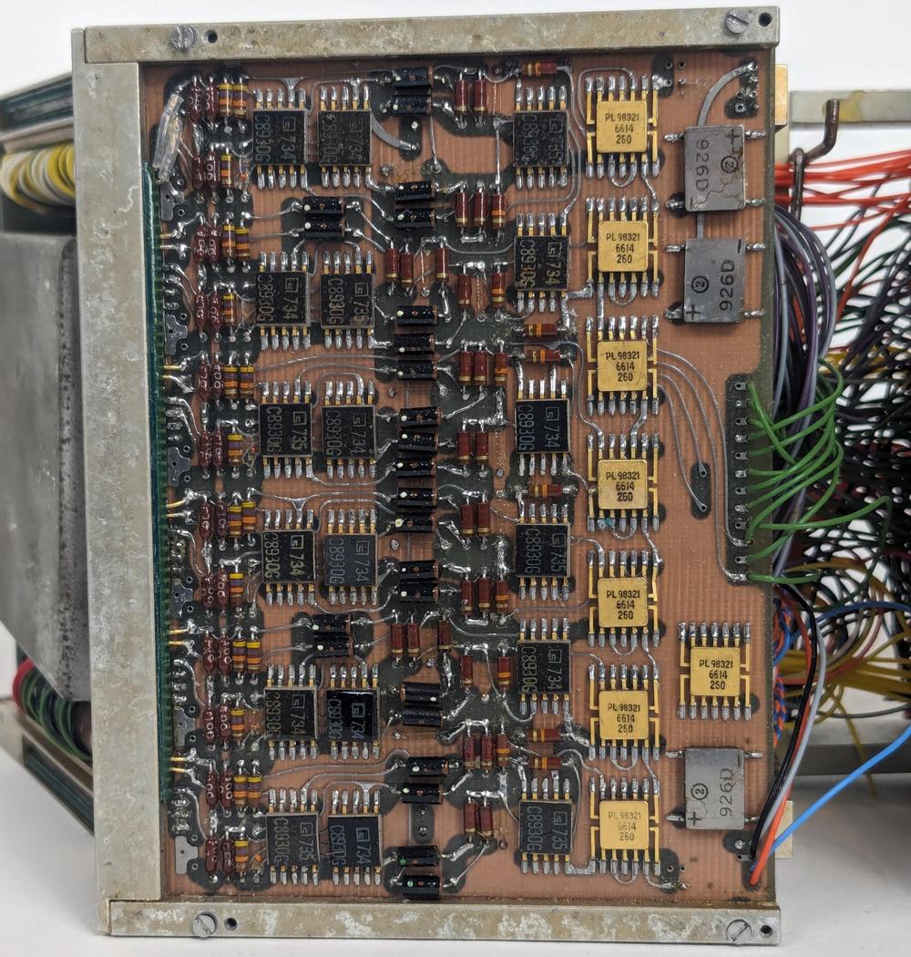
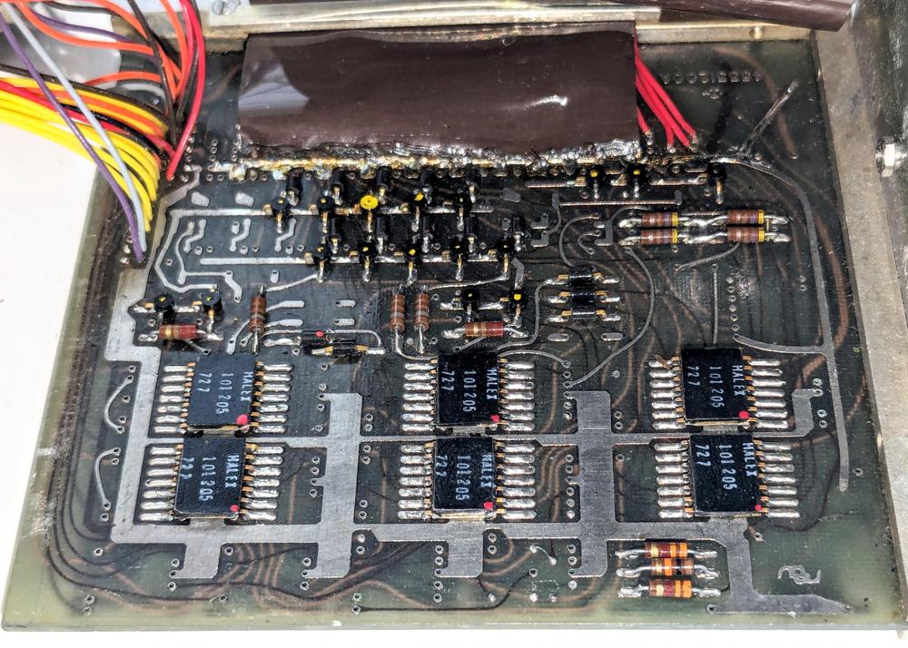
The analog board shown below sits next to the core memory stack. It uses a different set of flat-pack components: Signetics C8930G and PL 98321. Unfortunately, I could not identify these ICs. This board, unlike the previous boards, has a copper ground plane in the second layer of the circuit board; this layer is visible in the photo as the copper-colored background occupying most of the board.

Another analog board in the aviation computer.

Another analog board in the aviation computer.

Core memory

The unit is built around a core memory stack, as was common in the era before semiconductor memory took over. Magnetic core memory consists of a grid of tiny ferrite cores with wires threaded through them, forming a core plane. Typically, a core memory unit consists of multiple planes, one for each bit in the word, stacked to form a three-dimensional block of memory.

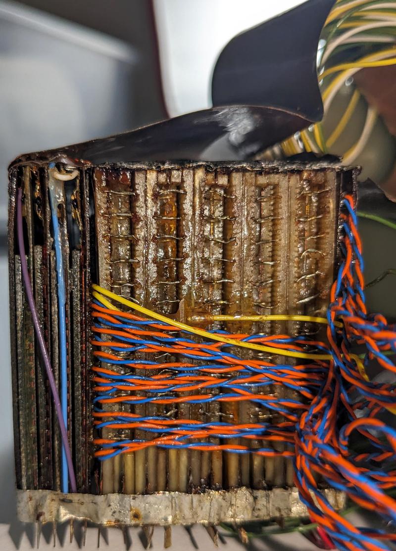
The photo below shows a closeup of the stack. It appears to have 20 planes, suggesting a 20-bit processor. Soldered wires connect the planes together to provide continuous wiring through the stack. The soldering on these wires looks somewhat haphazard, suggesting that this was not a production unit.

A closeup of the core memory stack. Brightly colored wires connect the module to the rest of the system. Small wires connect the layers together.

A closeup of the core memory stack. Brightly colored wires connect the module to the rest of the system. Small wires connect the layers together.

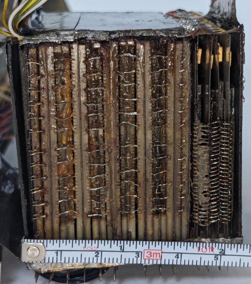
The photo below shows the other side of the core memory stack, with similar wiring between the planes. At the right are a few layers of a different type, connected with 26 wires. The tape measure shows that the core memory stack is compact, about 6 cm on a side (2¼").

Measurement of the core memory stack.

Measurement of the core memory stack.

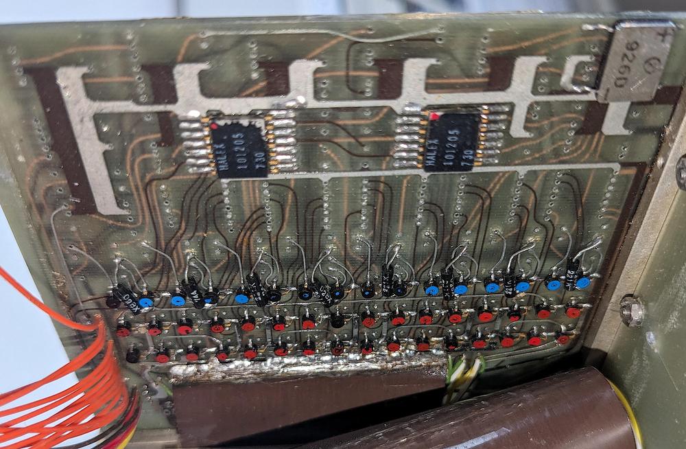
Some of the boards are drivers for the core memory stack. The board below has 48 small round transistors, colored either blue or red. Note the green, white, and yellow wires in the lower right, mostly hidden under the brown ground ribbon. These wires are connected to the core memory stack.

A circuit board with many small transistors.

A circuit board with many small transistors.

The board below also has numerous wires to the core stack, underneath the brown ground ribbon, so it is presumably another driver board. This board has some round driver transistors with yellow dots. Curiously, in the upper left there are a few circuit board pads where transistors could be mounted but are missing. Perhaps with the additional components the board would support a system with more of something: a larger keyboard? more memory?

A board with driver transistors.

A board with driver transistors.

Looking at the back of the unit, you can see the display indicator wiring at the top and a circuit board at the bottom. This board contains 20 transistors in metal cans, specifically Motorola 2N3736 NPN transistors. The core memory stack has 20 planes, matching the 20 transistors on this board, so the board probably implements the core memory "inhibit drivers", controlling the bit written to each plane. The board also has numerous tiny surface-mount transistors in white, red, and black packages. Close examination shows a few thin green "bodge" wires on this board, indicating that rework was performed on the board to fix a circuit problem, another piece of evidence that this unit is a prototype.

A view of the computer from the back, showing the display wiring and a circuit board.

A view of the computer from the back, showing the display wiring and a circuit board.

The core memory stack is enclosed by two sheet metal boxes, which I removed for the photos. The stack also has two flexible ground planes attached to it. The designers clearly wanted to ensure that the memory was well shielded, to a degree that I haven't seen in other systems.

Conclusions

Despite my research, this aerospace computer remains a mystery. I was unable to identify who manufactured it or even its exact function. One hypothesis is a NASA connection since NASA was extensively using these Signetics chips at the time. Moreover, this computer was obtained in the Houston area. Another hypothesis, based on the "CDC" label on the chips, is that this computer was built by Control Data's Aerospace Division. If you have any leads on this mysterious aviation computer, please contact me.

This system may have been a prototype. It has no part numbers, manufacturer name, or identifying plate.5 Moreover, the soldering on the core memory stack doesn't seem to be flight quality. Finally, the boards don't have conformal coating, which is typically used for spaceflight systems. However, the mechanical design looks advanced for a prototype, with dense boards that fold together like a book.

This unit clearly has a navigation role, but seems to be too inaccurate for an inertial navigation system (INS). It contains many integrated circuits, but not enough to form a full computer. I hypothesize that this unit contains the circuitry to drive the core memory and the display, and handle keyboard input. Looking at the underside of the unit (below), there are three connectors. I suspect these connectors were plugged into a larger box that held the computer itself.

A view of the underside of the electronics unit with the core memory wrapped in sheet metal.

A view of the underside of the electronics unit with the core memory wrapped in sheet metal.

The date codes on the integrated circuits range from 1966 to 1973, so the computer was probably manufactured in 1973. The seven-year range for date codes is a bit surprising, since integrated circuit technology changed a lot during these years. I suspect that the Signetics 400-series ICs had older date codes because this line didn't catch on so there was a lot of old stock rather than newly-manufactured parts. I also suspect that this system was designed around 1969, based on the multiple NASA systems using these chips then, suggesting that the design and manufacturing of this unit was a multi-year project.

Despite the lingering mysteries of this device, it provides an interesting example of aerospace computers at the beginning of the 1970s. Even though integrated circuits were primitive at the time, with just a few transistors per chip, aerospace computers used these chips and high-density packaging to build computers that were compact, reliable, and low power. These miniature computers controlled aircraft, missiles, and spacecraft, worlds away from the room-filling mainframes that attracted most of the attention.

Thanks to Usagi Electric for providing the aerospace computer. Eric Schlaepfer and Marc Verdiell helped with the analysis. Thanks to Don Straney for his research and comments. Various commenters on Reddit and Twitter provided suggestions. Follow me on Twitter @kenshirriff or RSS for updates. I'm also on Mastodon as oldbytes.space@kenshirriff.

Notes and references

  1. The indicators have a blank position, so there are 11 electromagnets. However, only the ten electromagnets associated with digits are used in the device. The N/S/E/W indicators have a square box in one of the positions, which probably is not used. 

  2. Signetics had multiple temperature ranges for the 400-series low-power ICs. The RE prefix indicated ultra high reliability aerospace components rated for a temperature range of -55°C to +125°C. The SE prefix on the chips in this unit indicated military airborne chips with the same temperature range. A NE or ST prefix indicated military prototype or industrial chips with a smaller temperature range (0°C to +70°C). A SP prefix indicated the commercial temperature rating, from +15°C to +55°C. A J suffix indicated a flat pack and an A suffix indicated a dual in-line pack (DIP). 

  3. NASA computers are the only documented systems that I could find that used these Signetics chips. One possible conclusion is that NASA was the only organization to use these chips. However, it is likely that other companies used these chips but didn't document them as thoroughly as NASA. That is, detailed circuitry for military aerospace computers is unlikely to be on the Internet. 

  4. Halex also made hybrid microcircuits, such as flip-flops, so these packages could be more complex than resistor networks. However, I think a resistor network is more likely. 

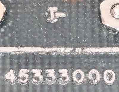
  5. One of the circuit boards had the number "45333000" on it, along with a symbol like "+I-", as shown below.

    Closeup of a circuit board showing a number, maybe identifying the board.

    Closeup of a circuit board showing a number, maybe identifying the board.

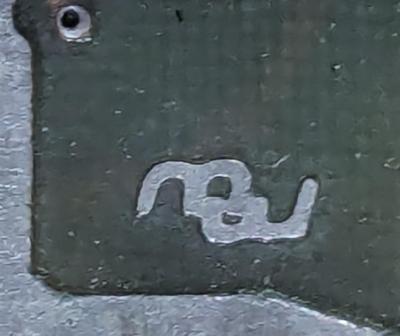
    One board also had a mysterious symbol that resembles "mw". I couldn't match these symbols to any manufacturers, and it is unclear if they are logos, fiducials, or other symbols.

    Closeup of a circuit board showing the "mw" mark.
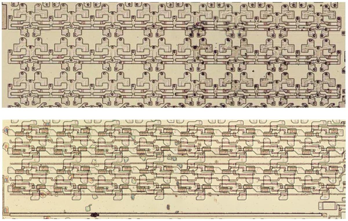
    Closeup of a circuit board showing the "mw" mark.
     

Talking to memory: Inside the Intel 8088 processor's bus interface state machine

In 1979, Intel introduced the 8088 microprocessor, a variant of the 16-bit 8086 processor. IBM's decision to use the 8088 processor in the IBM PC (1981) was a critical point in computer history, leading to the success of the x86 architecture. The designers of the IBM PC selected the 8088 for multiple reasons, but a key factor was that the 8088 processor's 8-bit bus was similar to the bus of the 8085 processor.1 The designers were familiar with the 8085 since they had selected it for the IBM System/23 Datamaster, a now-forgotten desktop computer, making the more-powerful 8088 processor an easy choice for the IBM PC.

The 8088 processor communicates over the bus with memory and I/O devices through a highly-structured sequence of steps called "T-states." A typical 8088 bus cycle consists of four T-states, with one T-state per clock cycle. Although a four-step bus cycle may sound straightforward, its implementation uses a complicated state machine making it one of the most difficult parts of the 8088 to explain. First, the 8088 has many special cases that complicate the bus cycle. Moreover, the bus cycle is really six steps, with two undocumented "extra" steps to make bus operations more efficient. Finally, the complexity of the bus cycle is largely arbitrary, a consequence of Intel's attempts to make the 8088's bus backward-compatible with the earlier 8080 and 8085 processors. However, investigating the bus cycle circuitry in detail provides insight into the timing of the processor's instructions. In addition, this circuitry illustrates the tradeoffs and implementation decisions that are necessary in a production processor. In this blog post, I look in detail at the circuitry that implements this state machine.

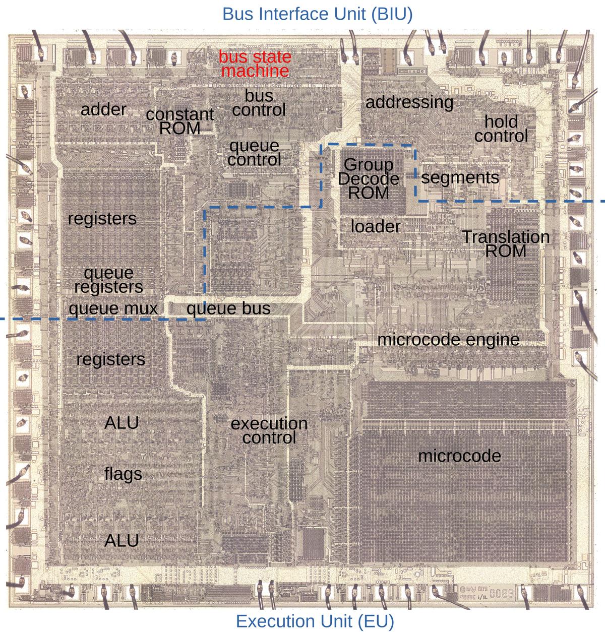
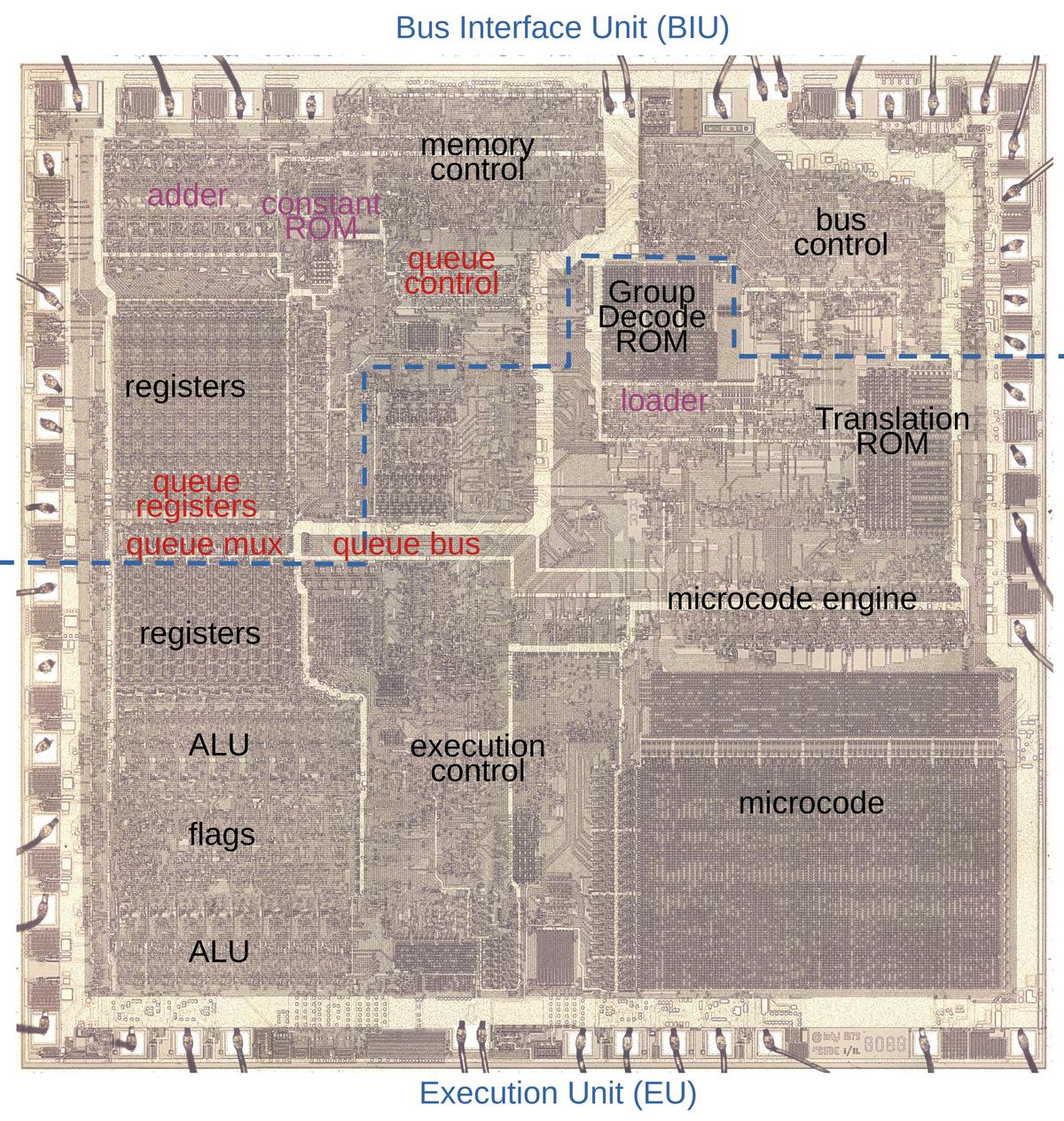
By examining the die of the 8088 microprocessor, I could reverse engineer the bus circuitry. The die photo below shows the 8088 microprocessor's silicon die under a microscope. Most visible in the photo is the metal layer on top of the chip, with the silicon and polysilicon mostly hidden underneath. Around the edges of the die, bond wires connect pads to the chip's 40 external pins. Architecturally, the chip is partitioned into a Bus Interface Unit (BIU) at the top and an Execution Unit (EU) below, with the two units running largely independently. The BIU handles bus communication (memory and I/O accesses), while the Execution Unit (EU) executes instructions. In the diagram, I've labeled the processor's key functional blocks. This article focuses on the bus state machine, highlighted in red, but other parts of the Bus Interface Unit will also play a role.

The 8088 die under a microscope, with main functional blocks labeled. This photo shows the chip's single metal layer; the polysilicon and silicon are underneath. Click on this image (or any other) for a larger version.

The 8088 die under a microscope, with main functional blocks labeled. This photo shows the chip's single metal layer; the polysilicon and silicon are underneath. Click on this image (or any other) for a larger version.

Although I'm focusing on the 8088 processor in this blog post, the 8086 is mostly the same. The 8086 and 8088 processors present the same 16-bit architecture to the programmer. The key difference is that the 8088 has an 8-bit data bus for communication with memory and I/O, rather than the 16-bit bus of the 8086. For the most part, the 8086 and 8088 are very similar internally, apart from trivial but numerous layout changes on the die. In this article, I'm focusing on the 8088 processor, but most of the description applies to the 8086 as well. Instead of constantly saying "8086/8088", I'll refer to the 8088 and try to point out places where the 8086 is different.

The bus cycle

In this section, I'll describe the basic four-step bus cycles that the 8088 performs.2 To start, the diagram below shows the states for a write cycle (slightly simplified3), when the 8088 writes to memory or an I/O device. The external bus activity is organized as four "T-states", each one clock cycle long and called T1, T2, T3, and T4, with specific actions during each state. During T1, the 8088 outputs the address on the pins. During the T2, T3, and T4 states, the 8088 outputs the data word on the same pins. The external memory or I/O device uses the T states to know when it is receiving address information or data over the bus lines.

A typical write bus cycle consists of four T states. Based on The 8086 Family Users Manual, B-16.

A typical write bus cycle consists of four T states. Based on The 8086 Family Users Manual, B-16.

For a read, the bus cycle is slightly different from the write cycle, but uses the same four T-states. During T1, the address is provided on the pins, the same as for a write. After that, however, the processor's data pins are "tri-stated" so they float electrically, allowing the external memory to put data on the bus. The processor reads the data at the end of the T3 state.

A typical read bus cycle consists of four T states. Based on The 8086 Family Users Manual, B-16.

A typical read bus cycle consists of four T states. Based on The 8086 Family Users Manual, B-16.

The purpose of the bus state machine is to move through these four T states for a read or a write. This process may seem straightforward, but (as is usually the case with the 8088) many complications make this process anything but easy. In the next sections, I'll discuss these complications. After that, I'll explain the state machine circuitry with a schematic.

Address calculation

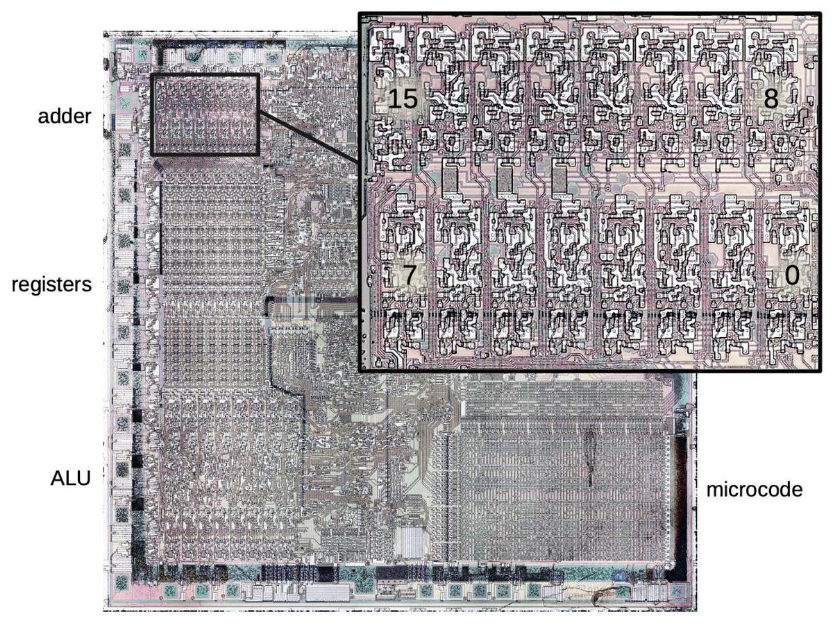
One of the notable (if not hated) features of the 8088 processor is segmentation: the processor supports 1 megabyte of memory, but memory is partitioned into segments of 64 KB for compatibility with the earlier 8080 and 8085 processors. The 8088 calculates each 20-bit memory address by adding the value of a segment register to a 16-bit offset. This calculation is done by a dedicated address adder in the Bus Interface Unit, completely separate from the chip's ALU. (This address adder can be spotted in the upper left of the earlier die photo.)

Calculating the memory address complicates the bus cycle. As the timing diagrams above show, the processor issues the memory address during state T1 of the bus cycle. However, it takes time to perform the address calculation addition, so the address calculation must take place before T1. To accomplish this, there are two "invisible" bus states before T1; I call these states "TS" (T-start) and "T0". During these states, the Bus Interface Unit uses the address adder to compute the address, so the address will be available during the T1 state. These states are invisible to the external circuitry because they don't affect the signals from the chip.

Thus, a single memory operation takes six clock cycles: two preparatory cycles to compute the address before the four visible cycles. However, if multiple memory operations are performed, the operations are overlapped to achieve a degree of pipelining that improves performance. Specifically, the address calculation for the next memory operation takes place during the last two clock cycles of the current memory operation, saving two clock cycles. That is, for consecutive bus cycles, T3 and T4 of one bus cycle overlap with TS and T0 of the next cycle. In other words, during T3 and T4 of one bus cycle, the memory address gets computed for the next bus cycle. This pipelining significantly improves the performance of the 8088, compared to taking 6 clock cycles for each bus cycle.

With this timing, the address adder is free during cycles T1 and T2. To improve performance in another way, the 8088 uses the adder during this idle time to increment or decrement memory addresses. For instance, after popping a word from the stack, the stack pointer needs to be incremented by 2.5 Another case is block move operations (string operations), which need to increment or decrement the pointers each step. By using the address adder, the new pointer value is calculated "for free" as part of the memory cycle, without using the processors regular ALU.4

Address corrections

The address adder is used in one more context: correcting the Instruction Pointer value. Conceptually, the Instruction Pointer (or Program Counter) register points to the next instruction to execute. However, since the 8088 prefetches instructions, the Instruction Pointer indicates the next instruction to be fetched. Thus, the Instruction Pointer typically runs ahead of the "real" value. For the most part, this doesn't matter. This discrepancy becomes an issue, though, for a subroutine call, which needs to push the return address. It is also an issue for a relative branch, which jumps to an address relative to the current execution position.

To support instructions that need the next instruction address, the 8088 implements a micro-instruction CORR, which corrects the Instruction Pointer. This micro-instruction subtracts the length of the prefetch queue from the Instruction Pointer to determine the "real" Instruction Pointer. This subtraction is performed by the address adder, using correction constants that are stored in a small Constant ROM.

The tricky part is ensuring that using the address adder for correction doesn't conflict with other uses of the adder. The solution is to run a special shortened memory cycle—just the TS and T0 states—while the CORR micro-instruction is performed.6 These states block a regular memory cycle from starting, preventing a conflict over the address adder.

A closeup of the address adder circuitry in the 8086. From my article on the adder.

A closeup of the address adder circuitry in the 8086. From my article on the adder.

Prefetching

The 8088 prefetches instructions before they are needed, loading instructions from memory into a 4-byte prefetch queue. Prefetching usually improves performance, but can result in an instruction's memory access being delayed by a prefetch, hurting overall performance. To minimize this delay, a bus request from an instruction will preempt a prefetch, even if the prefetch has gone through TS and T0. At that point, the prefetch hasn't created any bus activity yet (which first happens in T1), so preempting the prefetch can be done cleanly. To preempt the prefetch, the bus cycle state machine jumps back to TS, skipping over T1 through T4, and starting the desired access.

A prefetch will also be preempted by the micro-instruction that stops prefetching (SUSP) or the micro-instruction that corrects addresses (CORR). In these cases, there is no point in completing the prefetch, so the state machine cycle will end with T0.

Wait states

One problem with memory accesses is that the memory may be slower than the system's clock speed, a characteristic of less-expensive memory chips. The solution in the 1970s was "wait states". If the memory couldn't respond fast enough, it would tell the processor to add idle clock cycles called wait states, until the memory could respond.7 To produce a wait state, the memory (or I/O device) lowers the processor's READY pin until it is ready to proceed. During this time, the Bus Interface Unit waits, although the Execution Unit continues operation if possible. Although Intel's documentation gives the wait cycle a separate name (Tw), internally the wait is implemented by repeating the T3 state as long as the READY pin is not active.

Halts

Another complication is that the 8088 has a HALT instruction that halts program execution until an interrupt comes in. One consequence is that HALT stops bus operations (specifically prefetching, since stopping execution will automatically stop instruction-driven bus operations). A complication is that the 8088 indicates the HALT state to external devices by performing a special T1 bus cycle without any following bus cycles. But wait: there's another complication. External devices can take control of the bus through the HOLD functionality, allowing external devices to perform operations such as DMA (Direct Memory Access). When the device ends the HOLD, the 8088 performs another special T1 bus cycle, indicating that the HALT is still in effect. Thus, the bus state machine must generate these special T1 states based on HALT and HOLD actions. (I discussed the HALT process in detail here.)

Putting it all together: the state diagram

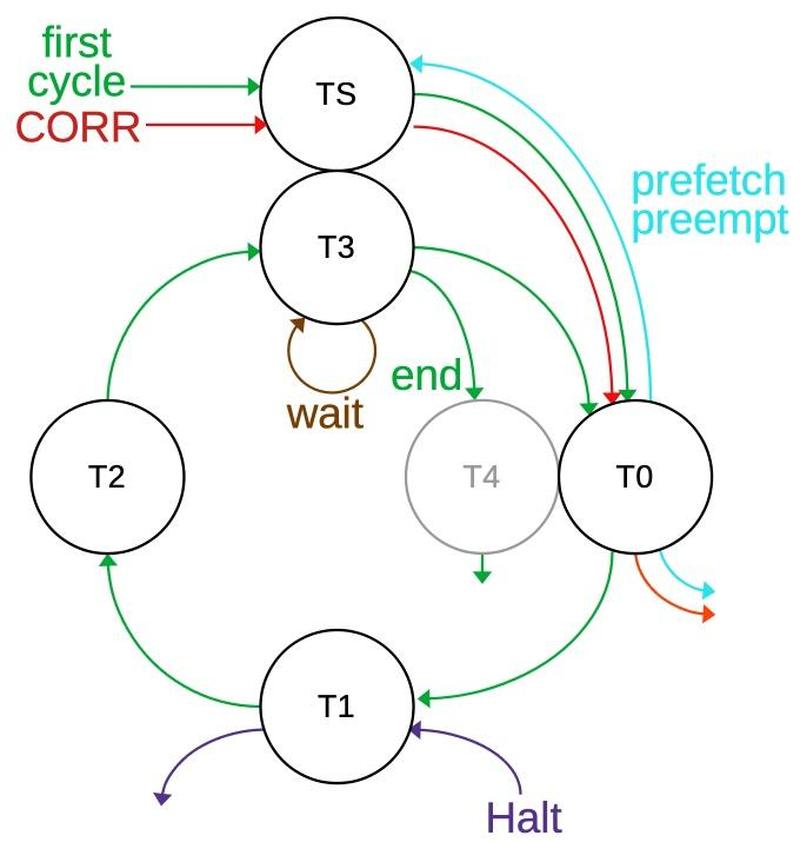
The state diagram below summarizes the different types of bus cycles. Each circle indicates a specific T-state, and the arrows indicate the transitions between states. The green line shows the basic bus cycle or cycles, starting in TS and then going around the cycle. From T3, a new cycle can start with T0 or the cycle will end with T4. Thus, new cycles can start every four clocks, but a full cycle takes six states (counting the "invisible" TS and T0). The brown line shows that the bus cycle will stay in T3 as long as there is a wait state. The red line shows the two cycles for a CORR correction, while the purple line shows the special T1 state for a HALT instruction. The cyan line shows that a prefetch cycle can be preempted after T0; the cycle will either restart at TS or end.

A state diagram showing the basic bus cycle and various complications.

A state diagram showing the basic bus cycle and various complications.

I'm showing states TS and T3 together since they overlap but aren't the same. Likewise, I'm showing T4 and T0 together. T4 is grayed out because it doesn't exist from the state machine's perspective; the circuitry doesn't take any particular action during T4.

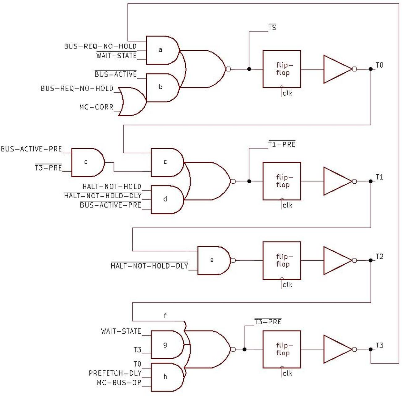
The schematic below shows the implementation of the state machine. The four flip-flops represent the four states, with one flip-flop active at a time, generating states T0, T1, T2, and T3 (from top to bottom). Each output feeds into the logic for the next state, with T3 wrapping back to the top, so the circuit moves through the states in sequence. The flip-flops are clocked so the active state will move from one flip-flop to the next according to the system clock. State TS doesn't have its own flip-flop, but is represented by the input to the T0 flip-flop, so it happens one clock cycle earlier.8 State T4 doesn't have a flip-flop since it isn't "real" to the bus state machine. The logic gates handle the special cases: blocking the state transfer if necessary or starting a state.
Schematic of the state machine.

Schematic of the state machine.

I'll explain the logic for each state in more detail. The circuitry for the TS state has two AND gates to generate new bus cycles starting from TS. The first one (a) causes TS to happen with T3 if there is a pending bus request (and no HOLD). The second AND gate (b) starts a bus cycle if the bus is not currently active and there is a bus request or a CORR micro-instruction. The flip-flop causes T0 to follow T3/TS, one clock cycle later.

The next gates (c) generate the T1 state following T0 if there is pending bus activity and the cycle isn't preempted to T3. The AND gate (d) starts the special T1 for the HALT instruction.9 The T2 state follows T1 unless T1 was generated by a HALT (e).

The T3 logic is more complicated. First, T3 will always follow T2 (f). Next, a wait state will cause T3 to remain in T3 (g). Finally, for a preempt, T3 will follow T0 (h) if there is a prefetch and a microcode bus operation (i.e. an instruction specified the bus operation).

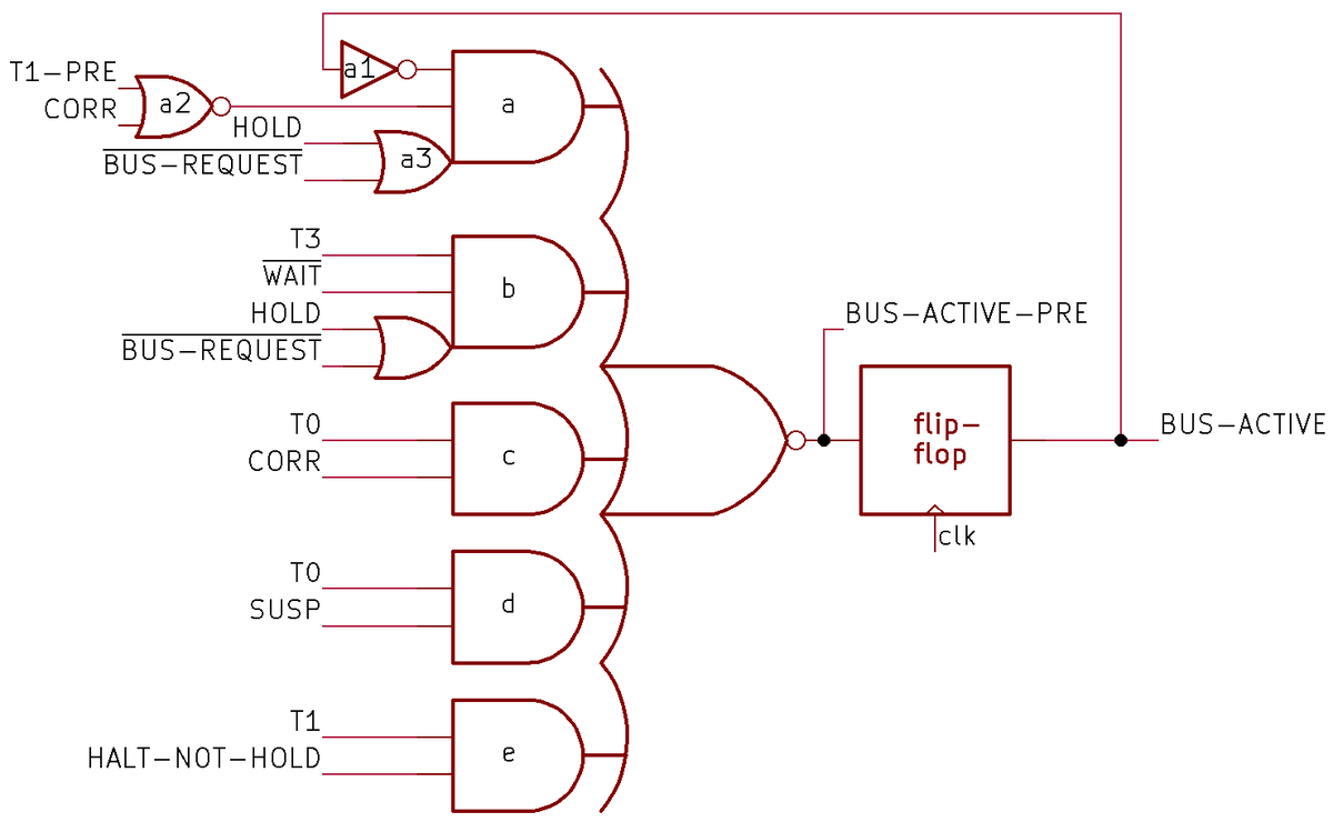
Next, I'll explain BUS-ACTIVE, an important signal that indicates if the bus is active or not. The Bus Interface Unit generates the BUS-ACTIVE signal to help control the state machine. The BUS-ACTIVE signal is also widely used in the Bus Interface Unit, controlling many functions such as transfers to and from the address registers. BUS-ACTIVE is generated by the complex circuit below that determines if the bus will be active, specifically in states T0 through T3. Because of the flip-flop, the computation of BUS-ACTIVE happens in the previous clock cycle.

The circuit to determine if the bus will be active next cycle.

The circuit to determine if the bus will be active next cycle.

In more detail, the signal BUS-ACTIVE-PRE indicates if the bus cycle will continue or will end on the next clock cycle. Delaying this signal through the flip-flop generates BUS-ACTIVE, which indicates if the bus is currently active in states T0 through T3. The top AND gate (a) is responsible for starting a cycle or keeping a cycle going (a1). It will allow a new cycle if there is a bus request (without HOLD) (a3). It will also allow a new cycle if there is a CORR micro-instruction prior to the T1 state (even if there is a HOLD, since this "fake" cycle won't use the bus) (a2). Finally, it allows a new cycle for a HALT, using T1-pre (a2).10 Next are the special cases that end a bus cycle. The second AND gate (b) ends the bus cycle after T3 unless there is a wait state or another bus request. (But a HOLD will block the next bus request.) The remaining gates end the cycle after T0 to preempt a prefetch if a CORR or SUSP micro-instruction occurs (d), or end after T1 for a HALT (e).

The BUS-ACTIVE circuit above uses a complex gate, a 5-input NOR gate fed by 5 AND gates with two attached OR gates. Surprisingly, this is implemented in the processor as a single gate with 14 inputs. Due to how gates are implemented with NMOS transistors, it is straightforward to implement this as a single gate. The inverter and NOR gate on the left, however, needed to be implemented separately, as they involve inversion; an NMOS gate must have a single inversion.

The bus state machine circuitry on the die.

The bus state machine circuitry on the die.

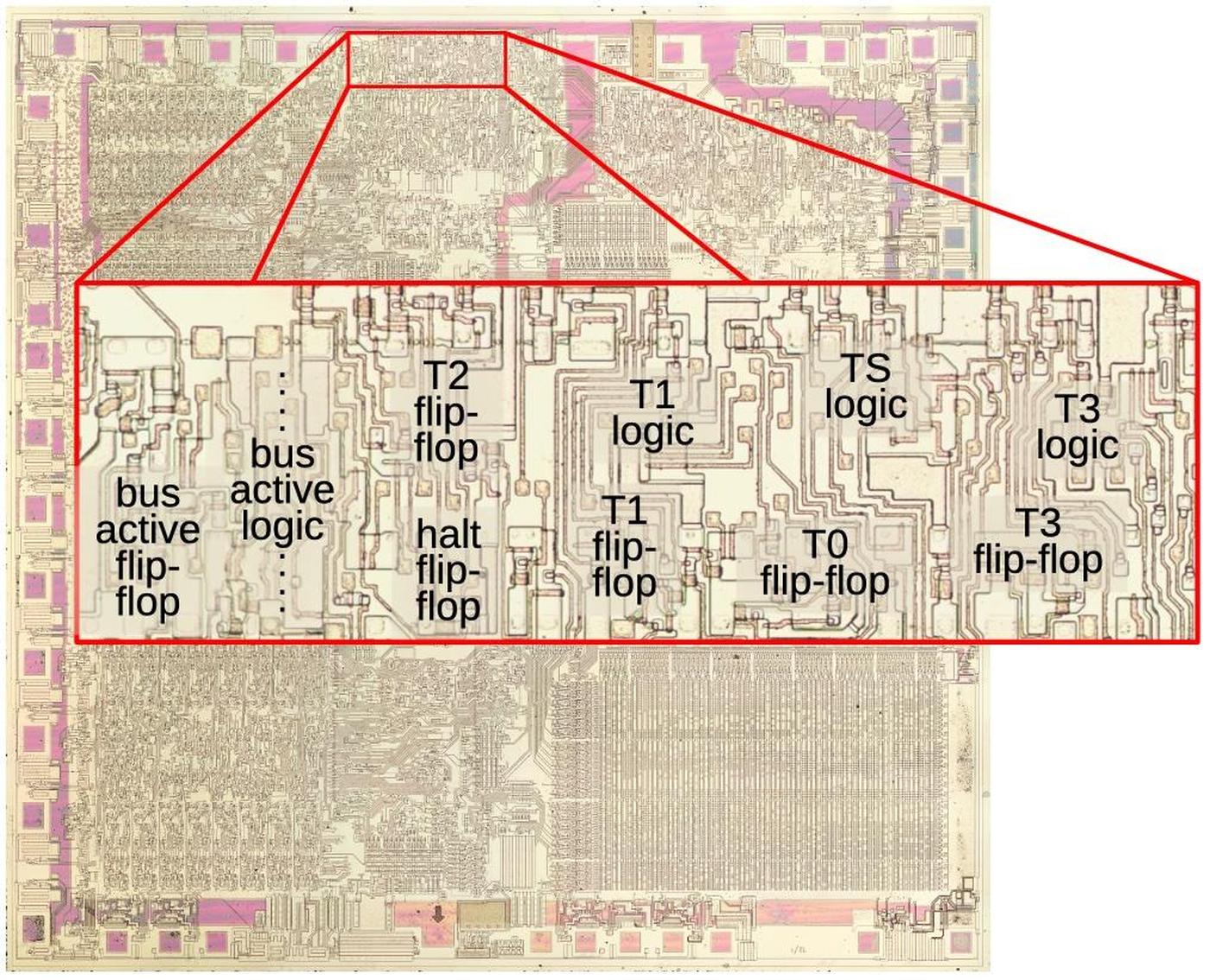
The diagram above shows the layout of the bus state machine circuitry on the die, zooming in on the top region of the die. The metal layer has been removed to expose the underlying silicon and polysilicon. The layout of each flip-flop is completely different, since the layout of each transistor is optimized to its surroundings. (This is in contrast to later processors such as the 386, which used standard-cell layout.) Even though the state machine consists of just a handful of flip-flops and gates, it takes a noticeable area on the die due to the large 3.2 µm feature size of the 8088. (Modern processors have features measured in nanometers, not micrometers.)

Conclusions

The bus state machine is an example of how the 8088's design consists of complications on top of complications. While the four-state bus cycle seems straightforward at first, it gets more complicated due to prefetching, wait states, the HALT instruction, and the bus hold feature, not to mention the interactions between these features. While there were good motivations behind these features, they made the processor considerably more complicated. Looking at the internals of the 8088 gives me a better understanding of why simple RISC processors became popular.

The bus state machine is a key part of the read and write circuitry, moving the bus operation through the necessary T-states. However, the state machine is not the only component in this process; a higher-level circuit decides when to perform a read, write, or prefetch, as well as breaking a 16-bit operation into two 8-bit operations.11 These circuits work together with the higher-level circuit telling the state machine when to go through the states.

In my next blog post, I'll describe the higher-level memory circuit so follow me on Twitter @kenshirriff or RSS for updates. I'm also on Mastodon as oldbytes.space@kenshirriff. If you're interested in the 8086, I wrote about the 8086 die, its die shrink process, and the 8086 registers earlier.

Notes and references

  1. The 8085 and 8088 processors both use a 4-step bus cycle for instruction fetching. For other reads and writes, the 8085's bus cycle has three steps compared to four for the 8088. Thus, the 8085 and 8088 bus cycles are similar but not an exact match. 

  2. The 8088 has separate instructions to read or write an I/O device. From the bus perspective, there's no difference between an I/O operation and a memory operation except that a pin on the chip indicates if the operation is for memory or I/O.

    The 8088 supports I/O operations for historical reasons, going back through the 8086, 8080, 8008, and the Datapoint 2200 system. In contrast, many other contemporary processors such as the 6502 used memory-mapped I/O, using standard memory accesses for I/O devices.

    The 8086 has a pin M/IO that is high for a memory access and low for an I/O access. External hardware uses this pin to determine how to handle the request. Confusingly, the pin's function is inverted on the 8088, providing IO/M. One motivation behind the 8088's 8-bit bus was to allow reuse of peripherals from the earlier 8-bit 8085 processor. Thus, the pin's function was inverted so it matched the 8085. (The pin is only available when the 8086/8088 is used in "minimum mode"; "maximum mode" remaps some of the pins, making the system more complicated but providing more control.) 

  3. I've made the timing diagram somewhat idealized so actions line up with the clock. In the real datasheet, all the signals are skewed by various amounts so the timing is more complicated. See the datasheet for pages of timing constraints on exactly when signals can change. 

  4. For more information on the implementation of the address adder, see my previous blog post

  5. The POP operation is an example of how the address adder updates a memory pointer. In this case, the stack address is moved from the Stack Pointer to the IND register in order to perform the memory read. As part of the read operation, the IND register is incremented by 2. The address is then moved from the IND register to the Stack Pointer. Thus, the address adder not only performs the segment arithmetic, but also computes the new value for the SP register.

    Note that the increment/decrement of the IND register happens after the memory operation. For stack operations, the SP must be decremented before a PUSH and incremented after a POP. The adder cannot perform a predecrement, so the PUSH instruction uses the ALU (Arithmetic/Logic Unit) to perform the decrement. 

  6. During the CORR micro-instruction, the Bus Interface Unit performs special TS and T0 states. Note that these states don't have any external effect, so they are invisible outside the processor. 

  7. The tradeoff with memory boards was that slower RAM chips were cheaper. The better RAM boards advertised "no wait states", but cheaper boards would add one or more wait states to every access, reducing performance. 

  8. Only the second half of the TS state has an effect on the Bus Interface Unit, so TS is not a full state like the other states. Specifically, a delayed TS signal is taken from the first half of the T0 flip-flop, and this signal is used to control various actions in the Bus Interface Unit. (Alternatively, you could think of this as an early T0 state.) This is why there isn't a separate flip-flop for the TS state. I suspect this is due to timing issues; by the time the TS state is generated by the logic, there isn't enough time to do anything with the state in that half clock cycle, due to propagation delays. 

  9. There is a bit more circuitry for the T1 state for a HALT. Specifically, there is a flip-flop that is set on this signal. On the next cycle, this flip-flop both blocks the generation of another T1 state and blocks the previous T1 state from progressing to T2. In other words, this flip-flop makes sure the special T1 lasts for one cycle. However, a HOLD state resets this flip-flop. That allows another special T1 to be generated when the HOLD ends. 

  10. The trickiest part of this circuit is using T1-pre to start a (short) cycle for HALT. The way it works is that the T1-pre signal only makes a difference if there isn't a bus cycle already active. The only way to get an "unexpected" T1-pre signal is if the state machine generates it for the first cycle of a HALT. Thus, the HALT triggers T1-pre and thus the bus-active signal. You might wonder why the bus-active uses this roundabout technique rather than getting triggered directly by HALT. The motivation is that the special T1 state for HALT requires the AND of three signals to ensure that the state is generated once for the HALT rather than continuously, but happens again after a HOLD, and waits until the current bus cycle is done. Instead of duplicating that AND gate, the circuit uses T1-pre which incorporates that logic. (This took me a long time to figure out.) 

  11. The 8088 has a 16-bit bus, compared to the 8088's 8-bit bus. Thus, a 16-bit bus operation on the 8088 will always require two 8-bit operations, while the 8086 can usually perform this operation in a single step. However, a 16-bit bus operation on the 8086 will still need to be broken into two 8-bit operations if the address is unaligned (i.e. odd). 

Inside an unusual 7400-series chip implemented with a gate array

When I look inside a chip from the popular 7400 series, I know what to expect: a fairly simple die, implemented in a straightforward, cost-effective way. However, when I looked inside a military-grade chip built by Integrated Device Technology (IDT)4 I found a very unexpected layout: over 1500 transistors in an orderly matrix. Even stranger, most of the die is wasted: less than 20% of these transistors are used, forming scattered circuits connected by thin metal wires.

In this blog post, I look at this chip in detail, describe its gates, and explain how it implements the "1-of-4" decoder function. I also discuss why it sometimes makes sense to build chips with a gate array design such as this, despite the inefficiency.

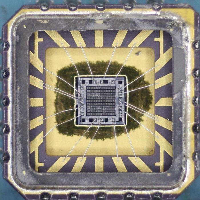
A photo of the tiny silicon die in its package.  This chip is the IDT 54FCT139ALB dual 1-of-4 decoder.  Click this image (or any other) for a larger version.

A photo of the tiny silicon die in its package. This chip is the IDT 54FCT139ALB dual 1-of-4 decoder. Click this image (or any other) for a larger version.

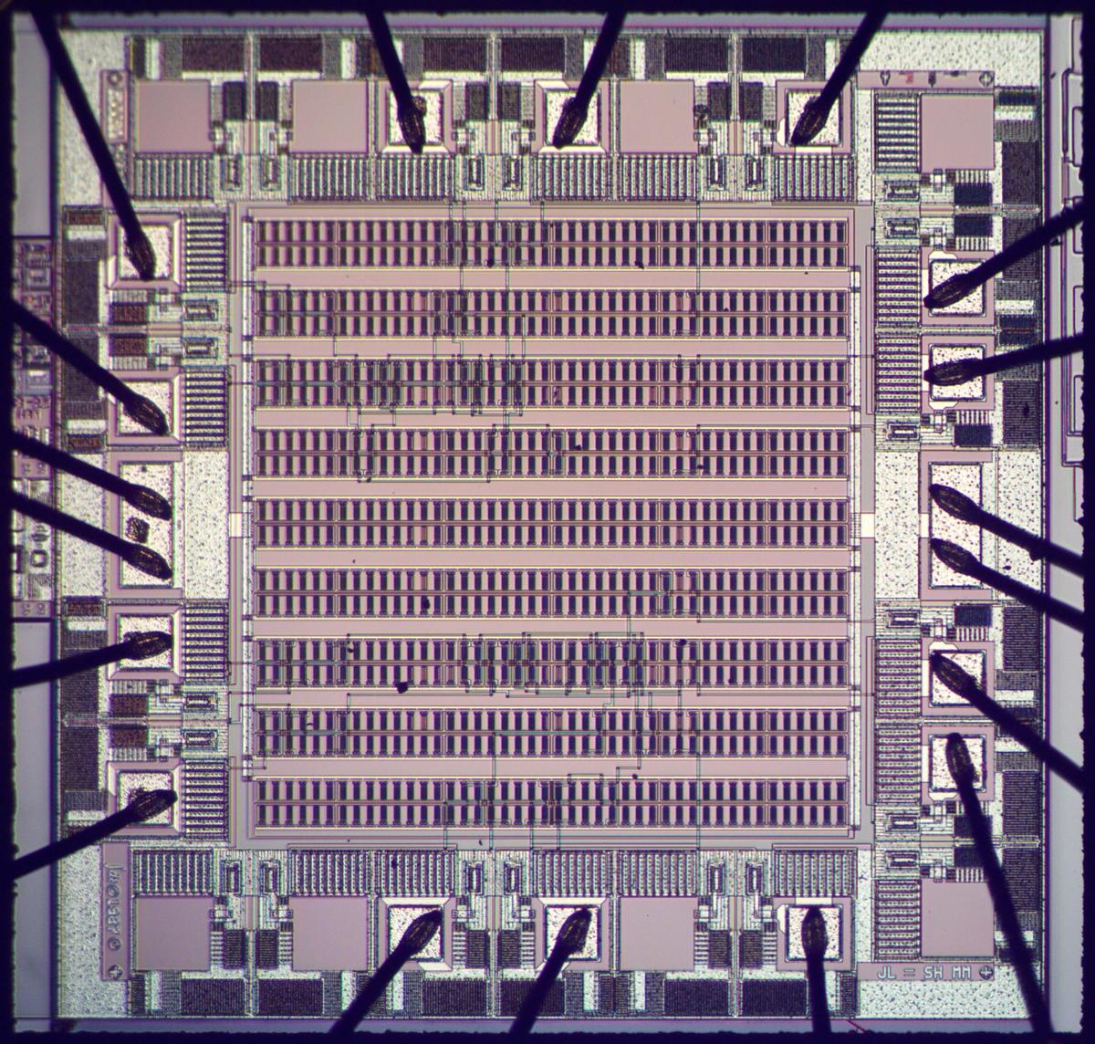
In the photo below, you can see the silicon die in more detail, with the silicon appearing pink. The main circuitry is implemented in the nine rows that form the gate array, a grid of 1584 transistors. The tiny dark rectangles are transistors of two types, NMOS and PMOS, that work together to implement CMOS logic circuits. At this scale, the metal wiring is visible as faint gray lines and smudges, but most of the transistors are unconnected. Surrounding the gate array are 22 input/output (I/O) blocks each with a square bond pad. As with the transistors, many of these I/O blocks are unused. Fourteen of these bond pads have tiny metal bond wires (the thick black lines) that connect the silicon die to the chip's external pins. Finally, the pairs of bond wires at the center left and center right provide ground and power connections for the chip.

Closeup die photo.

Closeup die photo.

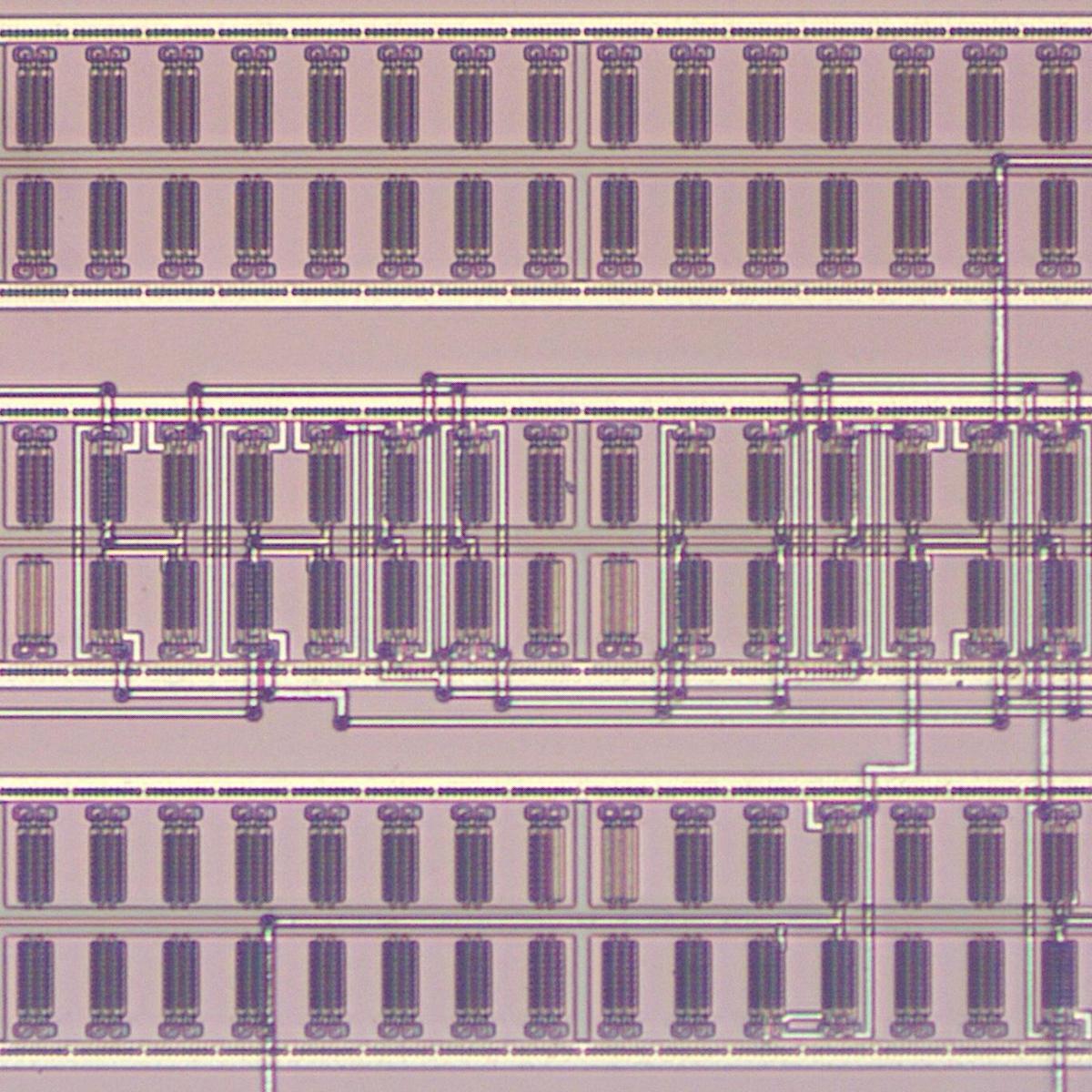
The photo below zooms in on three rows of circuitry in the chip. The large dark rectangles are pairs of transistors, with two lines of transistors in each row of circuitry. At the top and bottom of each row, the thick horizontal white lines are metal wiring that provides power and ground. In each row, one line of transistors holds PMOS transistors, next to the power wiring, while the other line holds NMOS transistors, next to the ground wiring. (The orientation flips in each successive row, so it isn't obvious which transistors are which unless you check the power connections at the end of the row.)

A closeup of the die.

A closeup of the die.

The transistors are wired into gates by the metal layers, the white lines. The gates are connected by horizontal and vertical wiring using the wiring channels between the rows. This wiring style is very similar to standard-cell logic. However, unlike standard-cell logic, the underlying transistor grid is fixed, resulting in wasted transistors. In the image above, most of the transistors in the middle row are used, while the top row is unused and the bottom row is mostly unused.

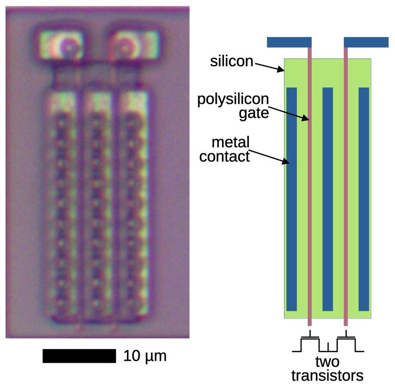
The diagram below shows the structure of one of the transistor blocks, which contains two tall, thin MOS transistors. The vertical metal contacts connect to the sources and drains of the transistors, with the two transistors sharing the middle contact. (On an integrated circuit, the source and drain of a transistor are identical, so it is arbitrary which side is the source and which is the drain.) The short horizontal metal contacts at the top connect to the gates of the two transistors; the gates are made of polysilicon, which is barely visible in the die photo. The gates partition the active silicon (green), forming the transistors. The gate width is approximately 1 µm.

A block of two transistors as they appear on the die, along with a diagram showing the structure. The bar indicates a length of 10 µm.

A block of two transistors as they appear on the die, along with a diagram showing the structure. The bar indicates a length of 10 µm.

NAND gate

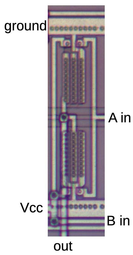
In this section, I'll explain the construction of one of the NAND gates on the die. The NAND gate below uses four transistors, two NMOS transistors on the top and two PMOS transistors on the bottom. The white lines are the metal wiring, forming two layers. Most of the wiring (including power and ground) is in the lower (M1) layer. The slightly wider and darker vertical segments are the upper (M2) layer. The circles connect the metal layers when they join, or connect the metal layer to the underlying silicon or polysilicon. With two metal layers, it's a bit tricky to see how the wiring is connected. The A and B inputs each connect to two transistor gates. The transistor group at the top is connected to ground on the right, with the output on the left. The transistor group on the bottom is connected to Vcc on the left and right, with the output in the middle. This has the effect of putting the upper transistors in series and the lower transistors in parallel.

A NAND gate on the die.

A NAND gate on the die.

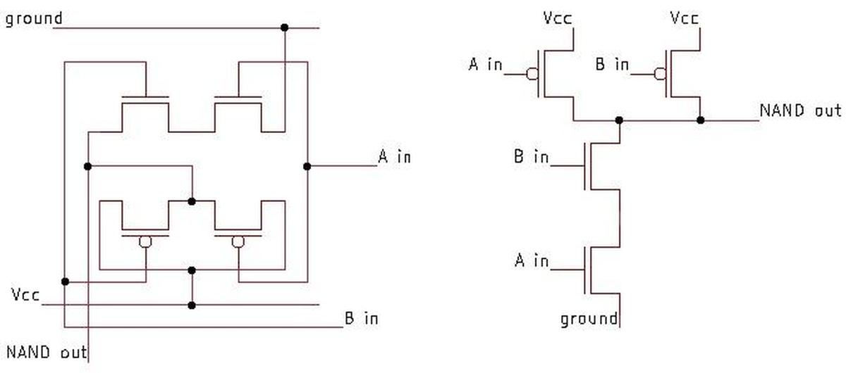
Below, I've drawn the schematic of the NAND gate. On the left, the layout of the schematic matches the die layout above. On the right, I've redrawn the schematic with a more traditional layout. To understand its operation, note that a PMOS transistor (top on the right schematic) turns on when the input is low, while an NMOS transistor (bottom on the right) turns on when the input is high. When both inputs are high, the two NMOS transistors turn on, connecting ground to the output, pulling it low. When either input is low, one of the PMOS transistors turns on, pulling the output high. Thus, the circuit implements the NAND function. The NMOS and PMOS transistors operate in a complementary fashion, giving CMOS (Complementary MOS) its name.

Schematic of a NAND gate.

Schematic of a NAND gate.

NOR gate

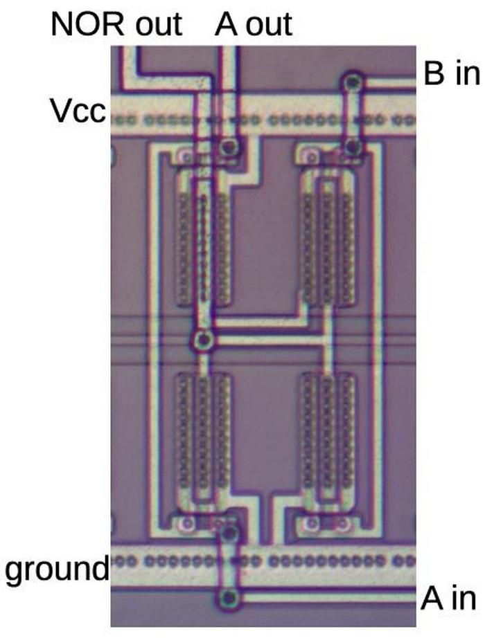
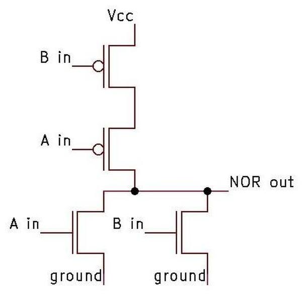
In this section, I'll explain the layout of one of the NOR gates on the die, shown below. This gate is twice as large as the previous NAND gate so it can provide twice the output current.1 The NOR gate uses eight transistors, four PMOS transistors in the upper half and four NMOS transistors in the lower half. (Note that Vcc and ground are flipped compared to the previous gate, as are the NMOS and PMOS transistors.) The two transistors in each block are wired in parallel to produce more current for the output. (A out is the same signal as A in, exiting the block at the top to connect to other circuitry.)

A NOR gate on the die.

A NOR gate on the die.

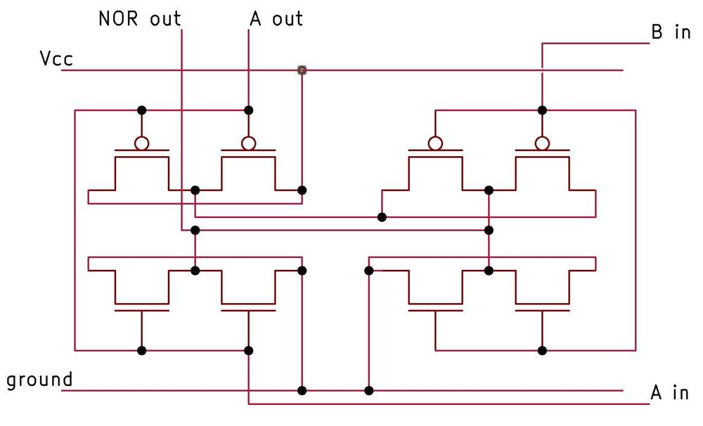
The schematic below shows the wiring of the eight transistors. The schematic layout corresponds to the physical layout to make it easier to map between the image and the schematic. The upper transistor groups are wired in series, while the lower transistor groups are wired in parallel.

Schematic corresponding to the gate above.

Schematic corresponding to the gate above.

The schematic below has been redrawn to make the functionality clearer, and the parallel transistors have been removed. If either input is high, one of the NMOS transistors on the bottom will turn on and pull the input low. If both inputs are low, the two PMOS transistors will turn on and pull the input high. This provides the desired NOR function.

Simplified NOR gate schematic.

Simplified NOR gate schematic.

Note that the NAND and NOR gates have similar but opposite schematics. In the NAND gate, the NMOS transistors are in series while the PMOS transistors are in parallel. In the NOR gate, the roles of the transistors are swapped.

The chip's circuit

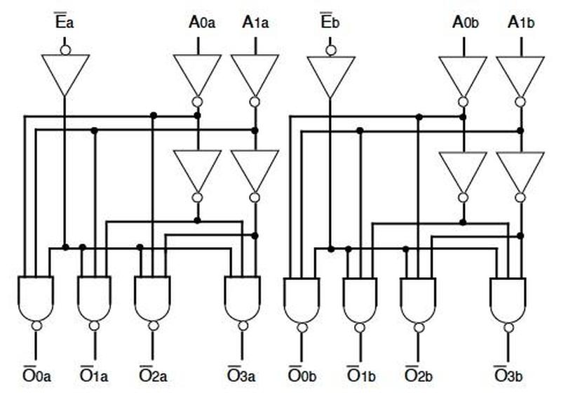
The chip I examined is a "dual 1-of-4 decoder with enable".2 The decoding function takes a two-bit input and selects one of four output lines depending on the binary value. The enable line must be low to activate this operation; otherwise all four output lines are disabled. The chip contains two of these decoders, which is why it is called a dual decoder. In total, the chip contains 18 logic gates,3 so it is very simple, even by 1990s standards.

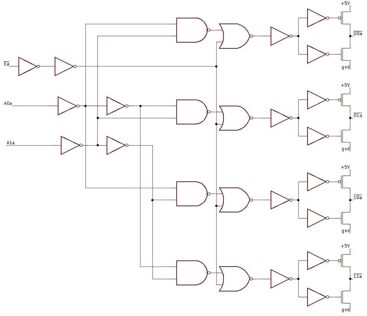
I reverse-engineered the chip and created the schematic below, showing one of the dual units. Each NAND gate matches one of the four input possibilities to drive one of the four outputs. The NOR gates support the ENABLE signal, blocking the outputs unless ENABLE is active (i.e. low).

Reverse-engineered schematic of half the chip.

Reverse-engineered schematic of half the chip.

The chip uses a general-purpose I/O block (below) for each pin, that can be used as an input or an output depending on how it is wired. Each block contains two large drive transistors: an NMOS transistor to pull the output low and a PMOS transistor to pull the output high. The I/O block has separate control lines for the two output transistors. (At the bottom of the image below, two thin metal wires drive the high-side and low-side transistors.) This permits tri-state logic: if neither transistor is energized, the output is left floating. The gate array drives the output transistors with high-current inverter, constructed from multiple transistors in parallel. (This is why the schematic shows more inverters than may seem necessary.)

One of the 22 I/O blocks on the die. Each I/O block is associated with a bond pad, where a bond wire can be connected to an external pin.

One of the 22 I/O blocks on the die. Each I/O block is associated with a bond pad, where a bond wire can be connected to an external pin.

When used as an input, the pad is wired to the surrounding circuitry slightly differently, connecting to input protection diodes (not shown on the schematic). Thus, the functionality of the I/O blocks can be changed by modifying the metal layers, without changing the underlying silicon.

Some 7400-series history

The earliest logic integrated circuits used resistors and transistors internally, so they were called RTL (Resistor Transistor Logic), but RTL had significant performance problems. RTL was rapidly replaced by Diode Transistor Logic (DTL) and then Transistor Transistor Logic (TTL). In 1964, Texas Instruments created a line of TTL integrated circuits for military applications called the SN5400 series. This was shortly followed by the commercial-grade SN7400 series.

The 7400 series of integrated circuits was inexpensive, fast, and easy to use. The line started with simple logic circuits such as four NAND gates on a chip, and moved into more complex chips such as counters, shift registers, and ALUs. The 7400 series became very popular in the 1970s and 1980s, used by electronics hobbyists and high-performance minicomputers alike. These chips became essential building blocks and "glue" logic for microcomputers, heavily used in the Apple II for instance.

The original 7400 series branched into dozens of families with different performance characteristics but the same functionality. The 74LS (low-power Schottky) family, for instance, became very popular as it both improved speed and reduced power consumption. In the mid-1970s, 7400-series chips were introduced that used CMOS circuitry instead of TTL for dramatically lower power consumption. This CMOS family, the 74C series, was followed by numerous other CMOS families.

That brings us to the chip I examined, a member of IDT's 74FCT (Fast CMOS TTL-compatible) line of chips, introduced in the mid-1980s. (Specifically, it is in the 54FCT family because it handles a wider temperature range.) These chips used advanced CMOS technology to provide high speed, low power consumption, and as a military option, radiation tolerance.

Conclusions

Why would you make a chip in this inefficient way, using a gate array that wastes most of the die area? The motivation is that most of the design cost can be shared across many different part types. Each step of integrated circuit processing requires an expensive mask for photolithography. With a gate array, all chip types use the same underlying silicon and transistors, with custom masks just for the two metal layers. In comparison, a fully custom chip might require eight custom masks, which costs much more. The tradeoff is that gate array chips are larger so the manufacturing cost is higher per device.5 Thus, a gate array design is better when selling chips in relatively small quantities, while a custom design is cheaper when mass-producing chips.6 IDT focused on the high-performance and military market rather than the commodity chip market, so gate arrays were a good fit.

One last thing. The packaging of this chip is very interesting since it is mounted on a multi-chip module. The module also contains two Atmel EEPROMs. Presumably the decoder chip decodes address bits to select one of the EEPROMs.

The multi-chip module containing the decoder chip along with an AT28HC64 EPROM on either side.

The multi-chip module containing the decoder chip along with an AT28HC64 EPROM on either side.

Thanks to Don S. for providing the chip. Follow me on Twitter @kenshirriff or RSS for updates. I've also started experimenting with Mastodon recently as @oldbytes.space@kenshirriff.

Notes and references

  1. Properly sizing the transistors in a gate is important for performance. Since the transistors in the gate array are all the same size, multiple transistors are used in parallel to get the desired current. The 1999 book Logical Effort describes a methodology for maximizing the performance of CMOS circuits by correctly sizing the transistors. 

  2. The part number is "IDT 54FCT139ALB". "54" indicates the chip operates under an enhanced temperature range of -55°C to +125°C. The "A" indicates the chip is 35% faster than the base series (but not as fast as "C"). "L" indicates the chip is packaged in a leadless chip carrier, the square package shown at the top of the article. Finally, "B" indicates the chip was tested according to military standards: MIL-STD-883, Class B. 

  3. The chip contains 18 logic gates according to the functional schematic in the datasheet (below). The implementation actually uses 52 logic gates by my count (2×26) because the implementation doesn't exactly match the schematic. In particular, the datasheet shows three-input NAND gates, but the chip uses a NAND gate and a NOR gate along with inverters. The chip also has additional inverters to drive the output transistors in each I/O block.

    Schematic of the chip from the datasheet.

    Schematic of the chip from the datasheet.


  4. Integrated Device Technology was a spinoff from Hewlett Packard that started in 1980. IDT built advanced CMOS chips including fast static RAM and microprocessors (bit-slice and MIPS). It became part of Renesas in 2018. A very detailed 1986 profile of IDT is here. IDT's logo is pretty cool, combining a chip wafer and calculus.

    The logo of Integrated Device Technology.

    The logo of Integrated Device Technology.

    Here's how the logo looks on the die:

    Closeup of the die showing the IDT logo.

    Closeup of the die showing the IDT logo.

    The die also has the initials of the designers, along with some mysterious symbols. One looks like the Chinese character "æ­£". (Update: based on a Twitter comment, these symbols are probably tally marks, indicating the revision count for each mask.)

    Closeups of two parts of the die.

    Closeups of two parts of the die.

  5. Integrated circuit manufacturing is partitioned into the "front end of line", where the transistors are created on the silicon wafer, and the "back end of line", where the metal wiring is put on top to connect the transistors. With a gate array construction, the front end of line steps create generic gate array wafers. The back end of line steps then connect the transistors as desired for a particular component. The gate array wafers can be produced in large quantities and stored, and then customized for specific products in smaller quantities as needed. This reduces the time to supply a particular chip type since only the back end of line process needs to take place. 

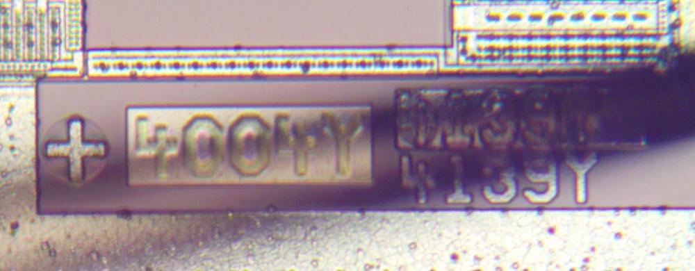
  6. The IDT High-Speed CMOS Logic Design Guide briefly mentions the gate array design. The FCT family was built from two sizes of gate arrays, "4004" for smaller chips and "8000" for larger chips. Later, IDT shrunk the original "Z-step" gate arrays to smaller, higher-performance "Y-step" arrays. They then customized some of the devices to create the "W-step" devices. Looking at the markings on the die, we see that this chip uses the "4004Y" gate array.

    The die shows gate slice 4004Y and part 4139Y (indicating 54139 or 74139). The numbers are slightly obscured by a bond wire.

    The die shows gate slice 4004Y and part 4139Y (indicating 54139 or 74139). The numbers are slightly obscured by a bond wire.


The Intel 8088 processor's instruction prefetch circuitry: a look inside

In 1979, Intel introduced the 8088 microprocessor, a variant of the 16-bit 8086 processor. IBM's decision to use the 8088 processor in the IBM PC (1981) was a critical point in computer history, leading to the dominance of the x86 architecture that continues to the present.1 One way that the 8086 and 8088 increased performance was by prefetching: the processor fetches instructions from memory before they are needed, so the processor can execute them without waiting on the relatively slow memory. I've been reverse-engineering the 8088 from die photos and this blog post discusses what I've uncovered about the prefetch circuitry.

The die photo below shows the 8088 microprocessor under a microscope. The metal layer on top of the chip is visible, with the silicon and polysilicon mostly hidden underneath. Around the edges of the die, bond wires connect pads to the chip's 40 external pins. I've labeled the key functional blocks; this article focuses on the prefetch queue components highlighted in red. The components in purple also play a role, and will be discussed below. Architecturally, the chip is partitioned into a Bus Interface Unit (BIU) at the top and an Execution Unit (EU) below. The BIU handles memory accesses, while the Execution Unit (EU) executes instructions. In particular, the BIU fetches instructions, which are transferred from the prefetch queue to the Execution Unit via the queue bus.

The 8088 die under a microscope, with main functional blocks labeled. This photo shows the chip's single metal layer; the polysilicon and silicon are underneath. Click on this image (or any other) for a larger version.

The 8088 die under a microscope, with main functional blocks labeled. This photo shows the chip's single metal layer; the polysilicon and silicon are underneath. Click on this image (or any other) for a larger version.

The 8086 and 8088 processors present the same 16-bit architecture to the programmer. The key difference is that the 8088 has an 8-bit data bus for communication with memory and I/O, rather than the 16-bit bus of the 8086. The 8088's narrower bus reduced performance, since the processor only transfers one byte at a time rather than two. However, the 8-bit bus enabled cheaper computer hardware. The 8-bit bus was also a better match for hardware based on the older but popular 8-bit Intel 8080 and 8085 processors, allowing the reuse of 8-bit I/O circuitry for instance. Much of the IBM PC was based on the little-known IBM DataMaster, a computer built around the Intel 8085. Thus, selecting the 8088 processor was a natural choice for the IBM PC.

For the most part, the 8086 and 8088 are very similar internally, apart from trivial but numerous layout changes on the die. The biggest differences are in the Bus Interface Unit, the circuitry that communicates with memory and I/O devices, since this circuitry handles 16 bits in the 8086 versus 8 bits in the 8088. There are a few microcode differences between the two chips. One interesting change is that for performance reasons the 8088 has a smaller prefetch queue than the 8086 (four bytes instead of six). (I wrote about the 8086's prefetch circuity earlier.)

Prefetching and the architecture of the 8086 and 8088

The 8086 and 8088 were introduced at an interesting point in microprocessor history, when memory was becoming slower than the CPU. For the first microprocessors, the speed of the CPU and the speed of memory were comparable.2 However, as processors became faster, the speed of memory failed to keep up. The 8086 was probably the first microprocessor to prefetch instructions to improve performance. While modern microprocessors have megabytes of fast cache3 to act as a buffer between the CPU and much slower main memory, the 8088 has just 4 bytes of prefetch queue. However, this was enough to substantially increase performance.

Prefetching had a major impact on the design of the 8086 and thus the 8088. Earlier processors such as the 6502, 8080, or Z80 were deterministic: the processor fetched an instruction, executed the instruction, and so forth. Memory accesses corresponded directly to instruction fetching and execution and instructions took a predictable number of clock cycles. This all changed with the introduction of the prefetch queue. Memory operations became unlinked from instruction execution since prefetches happen as needed and when the memory bus is available.

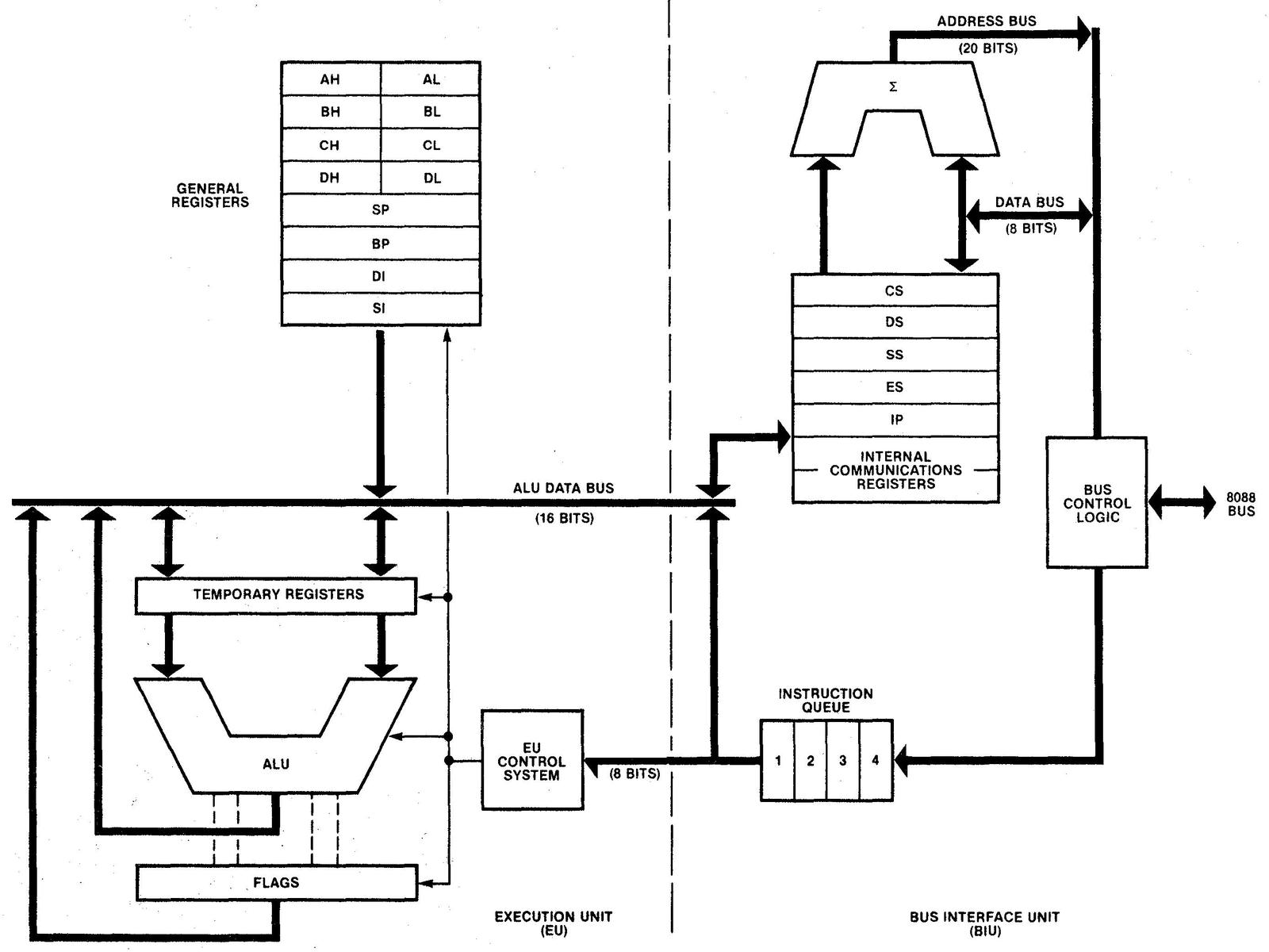
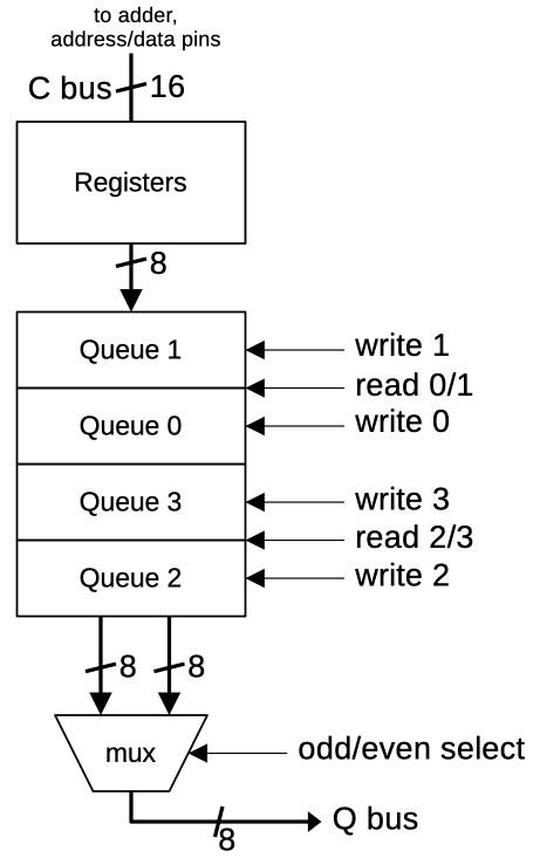
To handle memory operations and instruction execution independently, the implementors of the 8086 and 8088 divided the processors into two processing units: the Bus Interface Unit (BIU) that handles memory accesses, and the Execution Unit (EU) that executes instructions. The Bus Interface Unit contains the instruction prefetch queue; it supplies instructions to the Execution Unit via the Q (queue) bus. The BIU also contains an adder (Σ) for address calculation, adding the segment register base to an address offset, among other things. The Execution Unit is what comes to mind when you think of a processor: it has most of the registers, the arithmetic/logic unit (ALU), and the microcode that implements instructions. The segment registers (CS, DS, SS, ES) and the Instruction Pointer (IP) are in the Bus Interface Unit since they are directly involved in memory accesses, while the general-purpose registers are in the Execution Unit.

Block diagram of the 8088 processor.
This diagram differs from most 8088 block diagrams because it shows the actual physical implementation, rather than the programmer's view of the processor.
The "Internal Communication Registers" consist of the Indirect Register (IND) and the Operand Register (OPR). These hold a memory address and memory data value respectively.
From The 8086 Family User's Manual page 243.

Block diagram of the 8088 processor. This diagram differs from most 8088 block diagrams because it shows the actual physical implementation, rather than the programmer's view of the processor. The "Internal Communication Registers" consist of the Indirect Register (IND) and the Operand Register (OPR). These hold a memory address and memory data value respectively. From The 8086 Family User's Manual page 243.

It may seem inefficient for the Bus Interface Unit to have its own adder instead of using the ALU, but there are reasons for the separate adder. First, every memory access uses the adder at least once to add the segment base and offset. The adder is also used to increment the PC or index registers. Since these operations are so frequent, they would create a bottleneck if they used the ALU. Second, since the Execution Unit and the Bus Interface Unit run asynchronously with respect to each other, it would be complicated to share the ALU without conflicts.

Prefetching had another major but little-known effect on the 8086 architecture: the designers were considering making the 8086 a two-chip microprocessor. Prefetching, however, required a one-chip design because the number of control signals required to synchronize prefetching across two chips exceeded the package pins available. This became a compelling argument for the one-chip design that was used for the 8086.4 (The unsuccessful Intel iAPX 432, which was under development at the same time, ended up being a two-chip processor: one to fetch and decode instructions, and one to execute them.)

Implementing the queue

The 8088's instruction prefetch queue is implemented with four 8-bit queue registers along with two hardware "pointers" into the queue. One two-bit counter keeps track of the current read position from 0 to 3, i.e. the queue register that will provide the next instruction byte. The second counter keeps track of the current write position, i.e. the queue register that will receive the next instruction from memory.5 As bytes are fetched from the queue, the read pointer advances. As bytes are added to the queue, the write pointer advances.

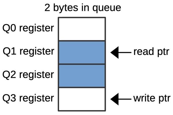
The diagram below shows an example queue configuration with two prefetched bytes. The middle two queue registers (Q1 and Q2) hold data. The read pointer indicates that the Execution Unit will get its next byte from Q1. The write pointer indicates that the next prefetched byte will go into Q3.

A queue configuration with two bytes in the prefetch queue. Bytes in blue hold prefetched data.

A queue configuration with two bytes in the prefetch queue. Bytes in blue hold prefetched data.

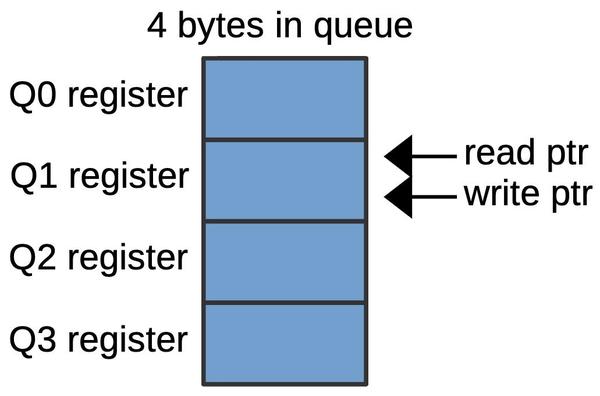
The diagram below shows how the queue pointers can wrap around. In this configuration, two more bytes have been written to the queue (Q3 and Q0), so the queue is full. The write pointer now points to Q1, the same as the read pointer.

A queue configuration with four bytes in the prefetch queue.

A queue configuration with four bytes in the prefetch queue.

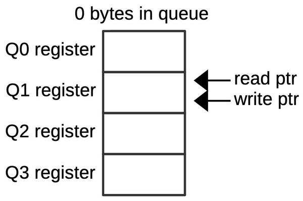
There is an important ambiguity, however. Suppose that four bytes are read from the queue, so the read pointer advances four positions, wrapping around back to Q1. The queue is now empty, as shown below, but the pointers have the same position as the full case above. Thus, if the read pointer and the write pointer both point to the same position, the queue may be empty or full. To distinguish these cases, a flip-flop is set if the queue enters the empty state. This flip-flop generates a signal that Intel called MT (empty).

A queue configuration with the queue empty.

A queue configuration with the queue empty.

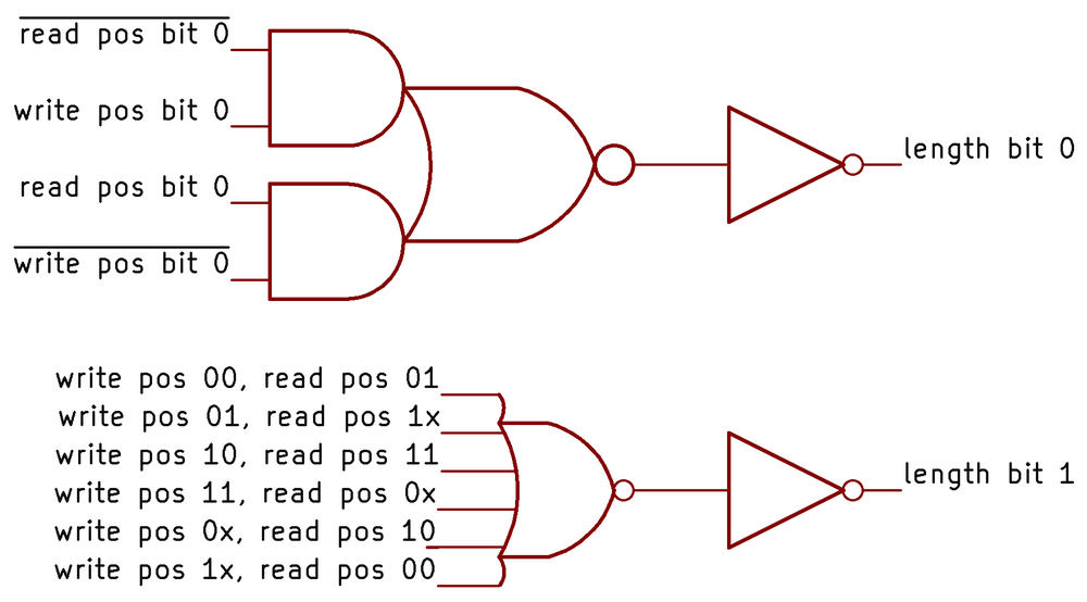
To determine how many bytes are in the queue, the queue circuitry uses a two-bit queue length value, along with the MT flip-flop value to distinguish the empty state. Conceptually, the queue length is generated by subtracting the read position from the write position. However, the implementation does not use a standard subtraction circuit, but instead uses hardcoded logic to determine the two bits of the length, as shown below.

The circuitry to determine the queue length.

The circuitry to determine the queue length.

The low bit of the length is the XOR of the two positions. In NMOS logic (used by the 8088), an AND-NOR gate is easy to implement, while an XOR gate is difficult. Thus, XOR is implemented as shown in the top circuit. (You can verify that if one input is 1 and the other is 0, the output is 1.) The high-order bit of the length is also based on an AND-NOR gate, one with six inputs. Each input is a combination of read and write positions that yields an output bit 1; each input is computed by a NOR gate, which I haven't drawn.6 As a result, the amount of logic circuitry to compute the length is fairly large.

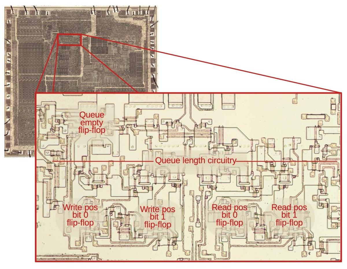
The diagram below zooms in on the queue control circuitry on the die, with the main flip-flops and circuitry labeled. The circuitry in the middle computes the queue length with the 6-input NOR gate stretched across the whole region. The flip-flops for the read and write positions are in the lower region. Despite the relative simplicity of the queue circuits, they take up a substantial part of the die. Compared to modern chips, the density of the 8088 is very low; you can almost see the flip-flops with the naked eye. But this isn't all the circuitry as prefetching also required queue registers and memory cycle control circuitry. Thus, prefetching was a moderately expensive feature for the 8088, as far as die area.

The queue and prefetch circuitry on the die. The metal layer has been removed for the closeup to show the silicon of the underlying transistors.

The queue and prefetch circuitry on the die. The metal layer has been removed for the closeup to show the silicon of the underlying transistors.

The loader

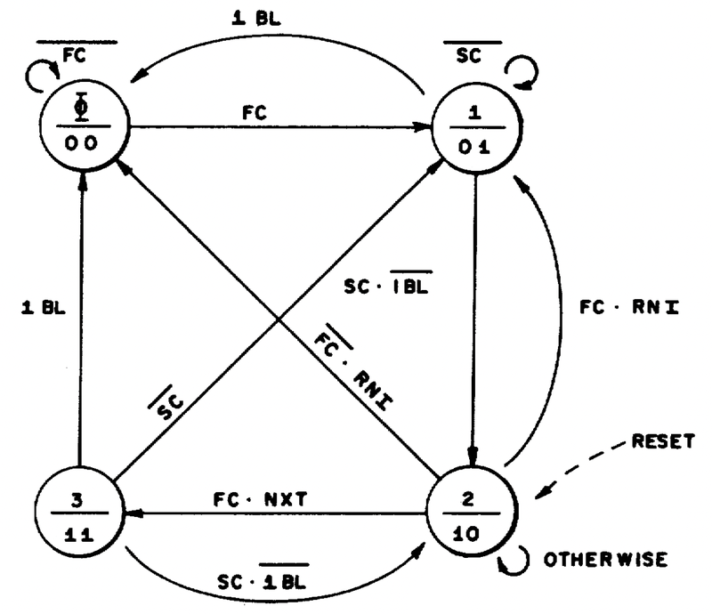
To decode and execute an instruction, the Execution Unit must get instruction bytes from the Bus Interface Unit, but this is not entirely straightforward. The main problem is that the queue can be empty, in which case instruction decoding must block until a byte is available from the queue. The second problem is that instruction decoding is relatively slow so it is pipelined. For maximum performance, the decoder needs a new byte before the current instruction is finished. A circuit called the "loader" solves these problems by providing synchronization between the prefetch queue and the instruction decoder. The loader uses a small state machine to efficiently fetch bytes from the queue at the right time and to provide timing signals to the decoder and microcode engine.

In more detail, as the loader requests the first two instruction bytes from the prefetch queue, it generates two timing signals that control the microcode execution. The FC (First Clock) indicates that the first instruction byte is available, while the SC (Second Clock) indicates the second instruction byte. Note that the First Clock and Second Clock are not necessarily consecutive clock cycles because the prefetch queue could be empty or contain just one byte, in which case the First Clock and/or Second Clock would be delayed. The instruction decoding circuitry and the microcode engine are controlled by the First Clock and Second Clock signals, so they remain synchronized with the bytes supplied by the prefetch queue.

At the end of a microcode sequence, the Run Next Instruction (RNI) micro-operation causes the loader to fetch the next machine instruction. However, fetching and decoding the next instruction is a bit slow so microcode execution would be blocked for a cycle. In many cases, this slowdown can be avoided: if the microcode knows that it is one micro-instruction away from finishing, it issues a Next-to-last (NXT) micro-operation so the loader can start loading the next instruction. This achieves a degree of pipelining in most cases; fetching the next instruction is overlapped with finishing the execution of the previous instruction.

The state machine for the 8086/8088 "loader" circuit.
The 1BL signal indicates a 1-byte instruction implemented in logic rather than microcode.
From patent US4449184.

The state machine for the 8086/8088 "loader" circuit. The 1BL signal indicates a 1-byte instruction implemented in logic rather than microcode. From patent US4449184.

The diagram above shows the state machine for the loader. I won't explain it in detail, but essentially it keeps track of whether it is waiting for a First Clock byte or a Second Clock byte, and if it is performing a fetch in advance (NXT) or at the end of an instruction (RNI). The state machine is implemented with two flip-flops to support its four states.

Microcode and the prefetch queue

The loader takes care of fetching an instruction that consists of an opcode byte and a Mod R/M (addressing mode) byte. However, many instructions have additional bytes or don't follow this format For example, an opcode such as "ADD AX" can be followed by an 8- or 16-bit immediate value, adding that value to the AX register. Or a "move memory to AX" instruction can be followed by a 16-bit memory address The microcode uses a separate mechanism for fetching these instruction bytes from the queue. Specifically, each micro-instruction contains a source register and a destination register that specify a data move. By specifying "Q" (the queue) as the source, a byte is fetched from the prefetch queue. If the queue is empty, microcode execution blocks until the Bus Interface Unit loads a byte into the prefetch queue. Thus, the complexity of instruction fetching and the prefetch queue is invisible to the microcode.7

A jump, subroutine call, or other control flow change causes the prefetch queue to be flushed since the queue contents are no longer useful. This is accomplished in microcode with the FLUSH micro-instruction, which resets the queue read and write pointers and sets the MT (empty) flip-flop. Note that the queue is flushed even if the target address is in the queue, for example if you jump one byte ahead.

One complication due to the prefetch queue is that the processor's Instruction Pointer points to the next instruction to be fetched, not the next instruction to be executed. This becomes a problem for a subroutine call, which needs to push the return address. It is also a problem for a relative jump, which is computed from the current instruction. The solution is the CORR micro-instruction, which corrects the Instruction Pointer by subtracting the queue length to determine the current execution position. This is implemented by the Bus Interface Unit, which holds correction constants in the Constant ROM, and subtracts them using the address adder (not the ALU).8

The queue registers

The 8086 and 8088 partition the registers into upper registers (in the Bus Interface Unit) and lower registers (in the Execution Unit). The upper registers are the registers associated with memory accesses (e.g. Instruction Pointer, segment registers) while the lower registers are more general purpose (e.g. AX, BX, SI, SP). The upper registers are connected to two 16-bit internal buses: the B bus and the C bus.

The queue registers are physically part of the upper registers, but are wired into the buses slightly differently, as shown below. In particular, the 8088's queue registers are written 8 bits at a time from the C bus. (In contrast, the 8086's queue registers can be written 16 bits at a time to support two-byte prefetches.) When accessing the queue, the queue registers are read 16 bits at a time, but only one byte is transferred to the Q bus for instruction processing.9

The queue registers in the 8088.

The queue registers in the 8088.

The diagram below shows how the queue registers appear on the die, comparing the six-byte prefetch queue in the 8086 (top) to the four-byte 8088 queue (bottom). The 8086 prefetch registers are structured as three rows of 16-bit registers, while the 8088 prefetch registers are structured as four rows of 8-bit registers. In both cases, each bit is stored in a cross-coupled pair of inverters. The bit lines (not present) are vertical, while the control lines to select a register are horizontal. The layout is different between the processors to support 16-bit versus 8-bit writes. Note the empty space at the bottom of the 8088 registers. Because the rest of the chips are mostly the same, the 8088 couldn't be "compacted" to avoid this wasted space.

The prefetch registers in the 8086 (top) and 8088 (bottom). For the 8086, the metal and polysilicon layers were removed, exposing the underlying silicon. For the 8088, the polysilicon and silicon are visible.

The prefetch registers in the 8086 (top) and 8088 (bottom). For the 8086, the metal and polysilicon layers were removed, exposing the underlying silicon. For the 8088, the polysilicon and silicon are visible.

Intel used simulations to determine the best queue sizes for the 8086 and 8088, balancing the performance cost of prefetching against the benefit. (The cost is that prefetching makes the bus unavailable for other memory or I/O operations.) The prefetch queue is discarded on a jump instruction or other change of control flow, causing the prefetched bytes to be wasted. Thus, as the queue gets longer, the chance of discarding a prefetched byte becomes larger, so the potential benefit of prefetching becomes smaller. Since the 8088 prefetches one byte at a time, compared to two bytes at a time on the 8086, prefetching on the 8088 costs twice as much as on the 8086 in terms of bus cycles used per byte. This changes the tradeoffs in favor of a shorter queue.

Because of the difference in queue lengths, the queue control circuitry is different between the 8086 and 8088. In particular, the 8086 needs three-bit counters for the read and write positions, while the 8088 uses two-bit counters. Because of this, the length computation circuitry is also different between the processors.

I plan to continue reverse-engineering the 8088 die so follow me on Twitter @kenshirriff or RSS for updates. I've also started experimenting with Mastodon recently as @oldbytes.space@kenshirriff. If you're interested in the 8086, I wrote about the 8086 die, its die shrink process and the 8086 registers earlier.

Notes and references

  1. Whenever I mention x86's domination of the computing market, people bring up ARM, but ARM has a lot more market share in people's minds than in actual numbers. One research firm says that ARM has 15% of the laptop market share in 2023, expected to increase to 25% by 2027. (Surprisingly, Apple only has 90% of the ARM laptop market.) In the server market, just an estimated 8% of CPU shipments in 2023 were ARM. See Arm-based PCs to Nearly Double Market Share by 2027 and Digitimes. (Of course, mobile phones are almost entirely ARM.) 

  2. Steve Furber, co-creator of the ARM chip, mentions that "The first integrated CPUs were coincidentally quite well matched to semiconductor memory speeds, and were therefore built without caches. This can now be seen as a temporary aberration." See VLSI Risc Architecture and Organization p77. To make this concrete, the Apple II (1977) used a MOS 6502 processor running at about 1 megahertz while its 4116 DRAM chips could perform an access in 250 nanoseconds (4 times the clock speed). The 8088 processor ran at 5-10 MHz which meant that 250 ns DRAM chips were slower than the clock speed. Nowadays, processors run at 4 GHz but DRAM access speed is about 50 nanoseconds (1/200 the clock speed). 

  3. Modern processors use caches to improve memory performance. Accessing data from a cache is faster than accessing it from main memory, but the tradeoff is that caches are much smaller than main memory. The prefetch queues in the 8086 and 8088 are similar to a cache in some ways, but there are some key differences. First, the prefetch queue is strictly sequential. If you jump ahead two bytes, even if the prefetch queue has those instruction bytes, the processor can't use them. Second, the prefetch queue can't reuse bytes. If you have a 6-byte loop, even though all the code fits in the prefetch queue, it will be reloaded every time. Third, the prefetch queue doesn't provide any consistency. If you modify an instruction in memory a couple of bytes ahead of the PC, the 8086 or 8088 will run the old instruction if it's in the queue. 

  4. The design decisions for the 8086 prefetch cache (and many other aspects of the chip) are described in: J. McKevitt and J. Bayliss, "New options from big chips," in IEEE Spectrum, vol. 16, no. 3, pp. 28-34, March 1979, doi: 10.1109/MSPEC.1979.6367944. Prefetch provided a 50% performance benefit to the 8086. 

  5. The queue read process doesn't use an explicit read operation. Instead, the selected queue register continuously puts its value onto the queue bus. When the Execution Unit uses this byte, it sends an increment signal to the queue to advance the read pointer. If the queue empty (MT) flip-flop is set, the Execution Unit will wait until a byte is ready. 

  6. The NOR gates are used as AND gates, following DeMorgan's laws. For example to produce a 1 output for write position 00 and read position 01, the logic is: NOR(write bit 1', write bit 0', read bit 1', read bit 0). Note that the bits into the NOR gate are all inverted from the "desired" values; if they are all 0, the NOR output is 1. Thus, there are also some inverters on the inputs. 

  7. Arbitrary memory reads and writes are performed directly on memory, bypassing the prefetch queue. The 8086/8088 do not provide consistency; if you modify an instruction byte in memory and the byte is in the queue, the processor will execute the old byte. (This type of self-modifying code can be used to determine the queue length, distinguishing the 8086 from the 8088 in software.) 

  8. The Constant ROM is used for more than just address correction. For example, it is also used to increment the Instruction Pointer after a prefetch. Other constants are used for the 8088's string operations, which act on a block of memory. The index registers are incremented or decremented by 1 for bytes or 2 for words. When popping a value from the stack, the stack pointer is decremented using the Constant ROM. 

  9. Are the 8088's queue registers 16 bits wide or 8 bits wide? It's ambiguous, since the registers are written 8 bits at a time, but read 16 bits at a time. This implementation was probably selected to support the 8088's 8-bit bus while reusing as much of the 8086 design as possible. In particular, the 8088 can only prefetch one byte at a time, so writes need to happen a byte at a time. Thus, there are four control lines selecting which queue byte is written. (The 8088 could write to half of a 16-bit register but that would require moving the prefetched byte to the correct half of a 16-bit bus.) On the read side, it would make sense to have four read lines, selecting one byte from the 8088's queue. However, since the 8086 already had a multiplexer to select one byte from two, the 8088 designers probably felt it was easier to keep that circuit. And with the smaller queue on the 8088, there was no need to try to save space by removing the circuit. Thus, the queue has two read-select lines and a multiplexer control line. All these lines are controlled by the write position and read position flip-flops.