Germanium transistors: logic circuits in the IBM 1401 computer

How did computers implement logic gates in the 1950s? Computers were moving into the transistor age, but transistors were expensive so circuits were optimized to minimize the transistor count. At the time, they didn't even use silicon transistors; germanium transistors were used instead. In this blog post, I'll describe one way that logic gates were implemented back then: diode-transistor logic.

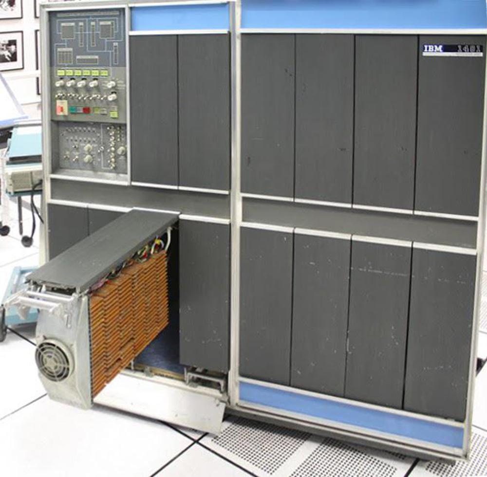
The IBM 1401 computer, showing some of the cards inside. (Click any image for a larger version.)

The IBM 1401 computer, showing some of the cards inside. (Click any image for a larger version.)

The IBM 1401 computer, above, was introduced in 1959 and became the most popular computer of the early 1960s, with more than 10,000 in operation. It was constructed from thousands of circuit cards, each implementing a function such as a few logic gates. The logic gates in the IBM 1401 use (for the most part) a simple form of logic called CTDL (Complemented Transistor Diode Logic) by IBM and DTL (Diode-Transistor Logic) by the rest of the world. As the names suggested, these gates are built from diodes in conjunction with a transistor.1

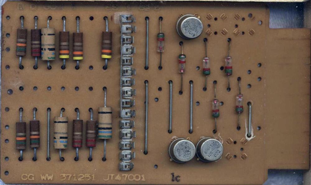
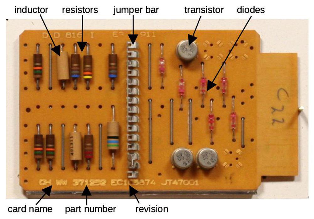
This SMS card (type CHWW) implements three NAND gates so there are three transistors.

This SMS card (type CHWW) implements three NAND gates so there are three transistors.

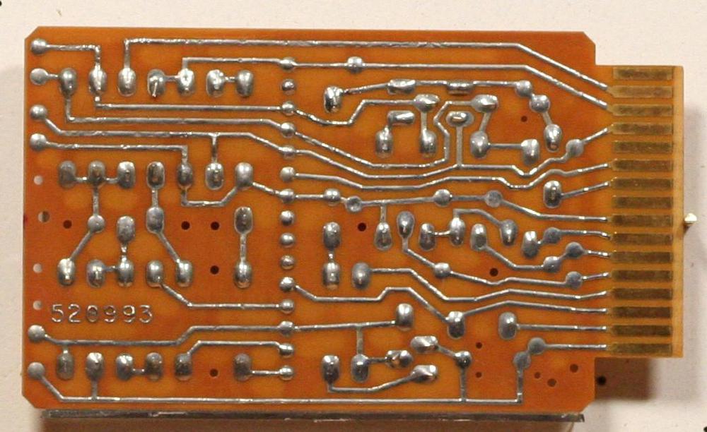
These cards are about the size of a playing card and called SMS cards, Standard Modular System.32 Each type of card has a code, typically four letters. The card above is a "CHWW" card, implementing three NAND gates. It contains a handful of components: transistors, diodes, resistors, and inductors. One unusual component is the jumper bar in the middle, called a "program cap". Breaking off tabs from this bar allowed the functionality of the card to be changed slightly so one card could fill multiple roles. The back of the card (below) shows the traces of the printed circuit board as well as the connector with 16 gold-plated contacts. More details of the CHWW card are in my SMS card database.

The back of the card has the PCB traces and the gold-plated edge connector.

The back of the card has the PCB traces and the gold-plated edge connector.

Logic circuit implementation

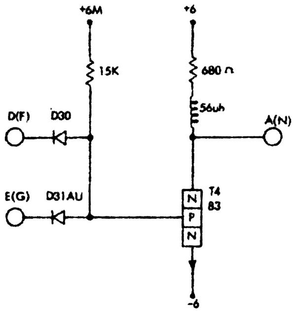
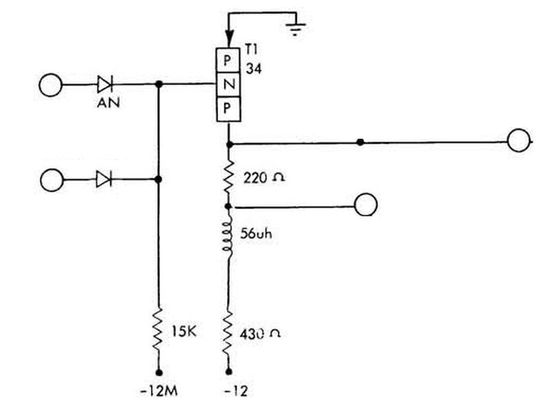
The CHWW card contains three NAND gates. The schematic below, from IBM's 1959 documentation, shows one of these gates. Note IBM's unusual symbol for a transistor, showing the N-P-N structure explicitly, with an external arrow for the emitter.

Schematic of a NAND logic circuit built from a type 83 transistor. From Standard Modular System Component Circuits, p43.

Schematic of a NAND logic circuit built from a type 83 transistor. From Standard Modular System Component Circuits, p43.

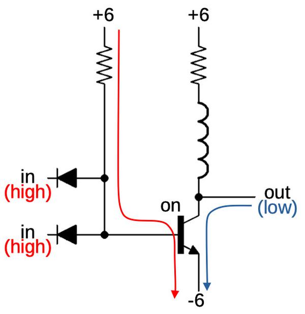
I've redrawn the schematic below using modern symbols. The arrows show (qualitatively) what happens when the gate has two high inputs. The left arrow indicates the current through the resistor and the transistor's base. This base current turns the transistor on, connecting the output to -6 volts, and producing a low output.

If both inputs are high, the output of the gate is low.

If both inputs are high, the output of the gate is low.

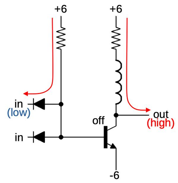
If there are one (or two) low inputs, however, the resistor's current flows out through the diode, rather than through the transistor. With the transistor off, the output is pulled high by the pull-up resistor. The result is a NAND gate: the output is low only if both inputs are high. In this circuit, the diodes are the components that compute the logic function.4 The transistor amplifies (and inverts) the result.5

If an input is low, the output of the gate is high.

If an input is low, the output of the gate is high.

There's a problem with this gate though. The output voltages are approximately +6 volts for a high signal and -6 volts for a low signal. You'd like the gate to switch when an input is roughly in the middle of this range. Unfortunately, the transistor in this circuit will switch when the input is around -6 volts. Thus, the input voltage and output voltage levels are incompatible and you can't connect two gates together.

There are several solutions to this problem. The first solution is to use additional diodes and transistors to shift the voltage levels to be compatible. Fairchild used this approach in their popular Micrologic line of DTL integrated circuits in the 1960s.9 The second solution (used in IBM's SDTDL circuits) is to shift the voltage levels by using additional resistors.

The 1401's gates, instead, uses a surprising solution that avoided extra components. In the gate above, the output voltage levels are raised up compared to the input. But a similar gate with PNP transistors instead of NPN transistors will have the opposite property: the output levels will be lowered. So IBM's solution was to alternate gates built with NPN transistors with gates built with PNP transistors. The first gate raises the voltage level up, and the second gate lowers it back down. You have twice as many types of gates, and it's more complex to design, but you avoid the expense of additional components.

The photo below shows the PNP-based NAND gate card. It is almost identical to the previous NPN card, except the transistors are PNP instead of NPN. The other difference is that it is powered with -12V and 0V instead of -6V and 6V.6

The CGWW NAND card is built with PNP transistors.

The CGWW NAND card is built with PNP transistors.

In more detail, for the NPN gate we first examined, the input switches around -6 volts, and the output is about -6 volts or 6 volts. In the corresponding PNP gate, the input switches around 0 volts, and the output is -12 volts or 0 volts. IBM called the -6V/6V levels type "T" and the 0V/12V levels type "U", so an NPN gate has a U input and a T output, while a PNP gate has a T input and a U output.7 By alternating NPN gates and PNP gates, you have T outputs going to T inputs and U outputs going to U inputs, and everything works.8

The diagram below shows part of the logic diagram from the 1401's adder, heavily simplified. Two type U signals go into the first CHWW gate, which outputs a T signal. The 4JMX gate is a PNP NAND gate that takes T inputs and outputs a U. The CRZV is an NPN buffer that converts U to T. Finally, CNWT is an NPN driver that amplifies a T signal, in this case a binary carry-out signal. Note how the signals alternate between T and U (except for the last special driver).

Simplified excerpt from an IBM ALD logic diagram, page 34.32.16.2.

Simplified excerpt from an IBM ALD logic diagram, page 34.32.16.2.

Wired-OR

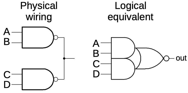
There's one more interesting trick with these logic gates: wired-OR. The idea is that you can wire the outputs of several NAND gates together. If any gate outputs a logical 0, that gate will pull the output low. If all gates output a logical 1, the output will be pulled high by the pull-up resistor. The resulting circuit implements an AND-OR-Invert gate. The diagram below illustrates how the NAND gates are wired together and how the circuit behaves logically. Wired-OR circuits are widely used in the 1401 because you get the OR gate "for free", minimizing circuitry.

An AND-OR-Invert gate. This shows two NAND gates but more can be connected.

An AND-OR-Invert gate. This shows two NAND gates but more can be connected.

There's one minor issue with wired-OR: if you wire standard NAND gates together, you end up with multiple pull-up resistors in parallel, which will affect the gate behavior. The solution is to use gates without pull-up resistors, except for one gate that has the pull-up resistor. For example, the 4JMX card has the pull-up resistor (called a "collector load"), while the 3JMX card lacks it. Thus, a wired-OR could use one 4JMX card and the rest would be 3JMX. (This is one reason why there are so many different types of SMS cards.)

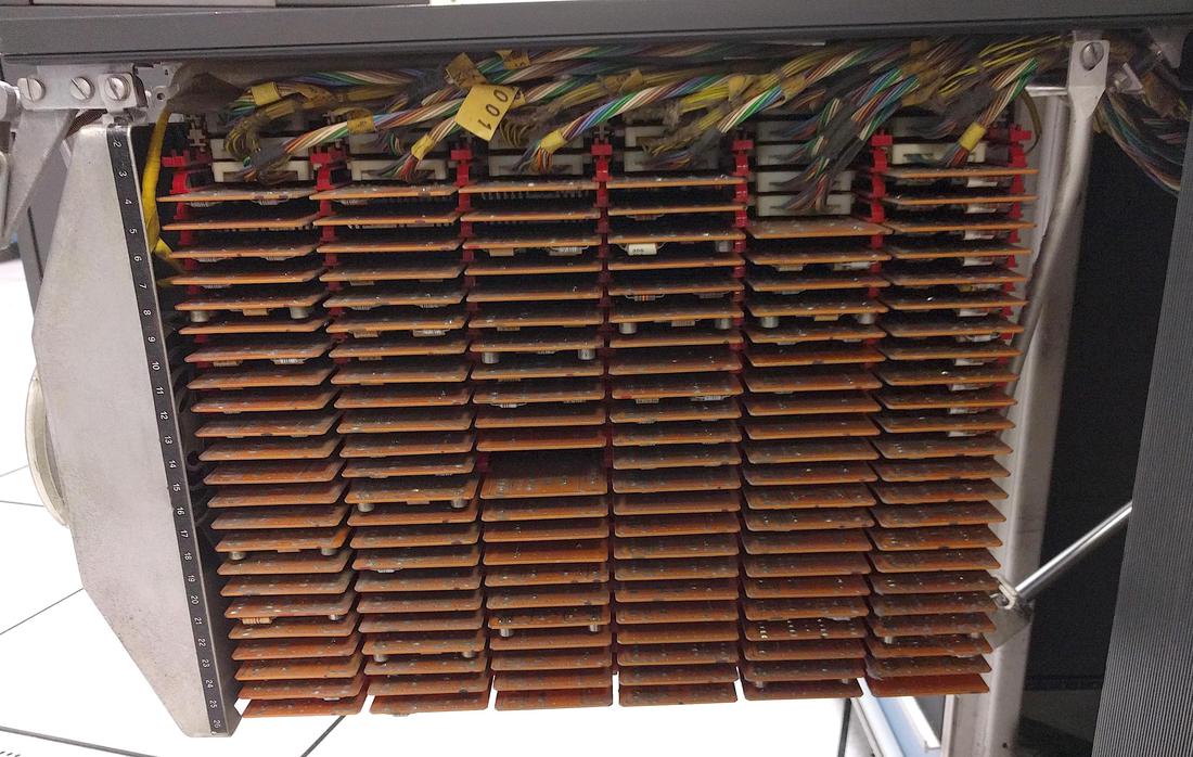
Since each card only implements a small amount of logic, the IBM 1401 computer requires thousands of cards. The photo below shows how they are mounted inside the computer. I won't go into more detail here about how SMS cards are combined to create functional units, but I've written about the circuitry in the 1401's adder if you want to learn more.

SMS cards installed in the IBM 1401 computer. The fan at the left keeps the cards cool.

SMS cards installed in the IBM 1401 computer. The fan at the left keeps the cards cool.

The transistors

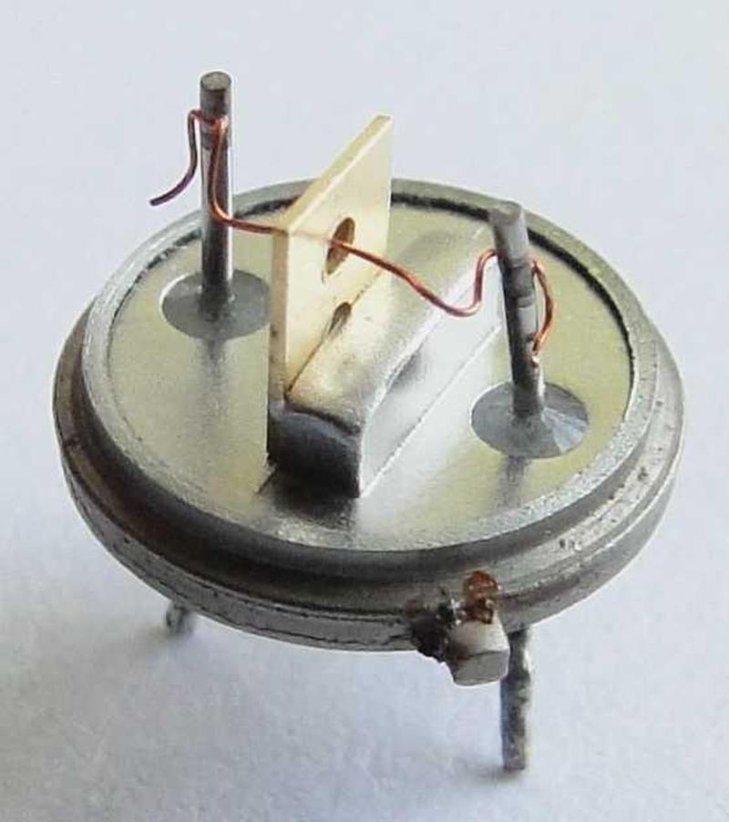
These gates use bipolar NPN and PNP transistors, types of transistors that are still used today. But the germanium alloy-junction transistors were completely different from modern silicon planar transistors. The photo below shows the construction of an NPN alloy transistor, It consists of a P-type germanium crystal base with tin/antimony beads fused on either side to form the emitter and collector. The regions of germanium-antimony alloy form the "N" regions. The resulting N-P-N layers form the NPN transistor. (A PNP transistor is formed similarly, using indium for the alloy.)10 In the photo, the vertical metal plate is the base contact with the tiny germanium disk in the circular hole. Copper wires are connected to the indium beads on either side of the germanium disk.

Inside a germanium alloy-junction transistor used in the IBM 1401 computer. This is an IBM type 083
NPN transistor. Photo from
  IBM 1401 restoration team

Inside a germanium alloy-junction transistor used in the IBM 1401 computer. This is an IBM type 083 NPN transistor. Photo from IBM 1401 restoration team

The 1950s were a time of rapid change in transistor technology. The transistor was invented at Bell Labs in 1947. General Electric invented the alloy junction transistor (used in the 1401) in 1950. In 1953, the drift transistor was created, faster because of its doping gradient. IBM used drift transistors in the Saturated Drift Transistor Diode Logic (SDTDL) family. The first silicon transistors were introduced in 1954. The wafer-based mesa transistor was invented in 1958, followed by the modern planar transistor in 1959. Thus, transistors were undergoing radical changes in the 1950s and IBM introduced new logic families to take advantage of these new transistor types.

Conclusion

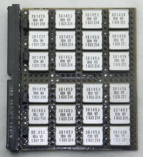
Diode-transistor logic was a key part of IBM's early computers such as the IBM 1401. In 1964, IBM introduced the groundbreaking System/360 line of mainframes. These computers still used diode-transistor logic, but instead of SMS cards with discrete components, the logic was encapsulated in small SLT modules (below) that contained tiny silicon transistors and diodes. An SLT module was roughly equivalent to an SMS card but just half an inch on a side and almost 100 times as reliable. The density, low cost, and reliability of SLT modules were important to the success of the System/360 line.

A board with 24 SLT modules on it, probably from the System/360. The 361453 modules implement AND-OR-Invert.

A board with 24 SLT modules on it, probably from the System/360. The 361453 modules implement AND-OR-Invert.

In the 1960s, diode-transistor logic integrated circuits were introduced. But DTL was soon eclipsed by the rise of TTL (transistor-transistor logic) in the late 1960s. In the 1970s, integrated circuits with MOS transistor logic became common, especially for microprocessors. CMOS logic took over in the 1980s and it's still the most popular logic family. Thanks to Moore's Law, technology has progressed from the IBM 1401 era with a few transistors on a board to modern microprocessors with billions of transistors on a chip.

The Computer History Museum in Mountain View, CA has two working 1401 computers, so stop by for a demo (once the pandemic is over). Thanks to bogomipz for suggesting this topic. Thanks to Randall Neff and Henk Stegeman for SMS card photos. I announce my latest blog posts on Twitter, so follow me @kenshirriff. I also have an RSS feed.

Notes and references

  1. IBM used a dizzying assortment of logic families in that era. Even the 1401 used multiple families (mostly the CTDL discussed above but also current-mode and STDTL in the TAU tape controller, and occasional SDTRL).

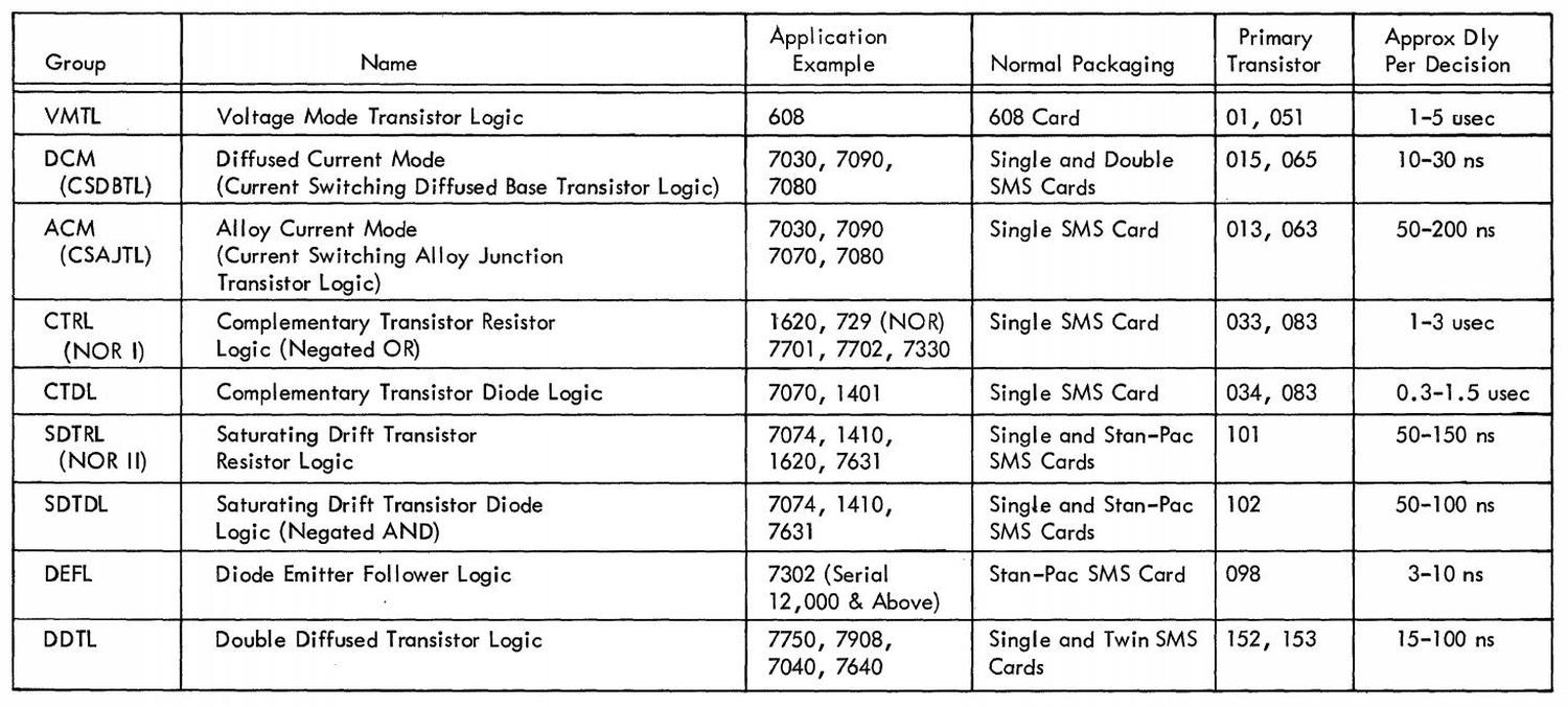
    The table below from 1963 summarizes IBM's numerous logic families. CTRL (Complemented Transistor Resistor Logic) used alloy-junction transistors. It was slow, operating below 200 kilohertz. CTDL (Complemented Transistor Diode Logic) also used alloy-junction transistors but operated up to 250 kilohertz. (The Complemented families alternate NPN and PNP circuits.) Current mode (similar to emitter-coupled logic) was much faster as transistors weren't saturated and the voltage swings were small (±.4V). It operated at 1 megahertz with alloy-junction transistors, and 7 megahertz with diffused junction transistors.

    IBM's logic families from DDTL Component Circuits, 1963, p5.

    IBM's logic families from DDTL Component Circuits, 1963, p5.

    For more discussion, see Transistor Component Circuits and Logic families in the 1401. There's an interesting discussion in Wikipedia's DTL talk page by William Crouse, who designed many of the SDTDL circuits at IBM. 

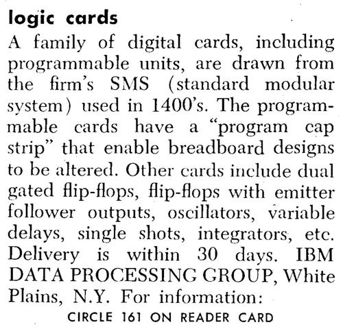
  2. IBM also offered SMS cards as components for other companies to use in products. The announcement below is from Datamation in 1966.

    A product announcement for SMS cards from Datamation, 1966.

    A product announcement for SMS cards from Datamation, 1966.


  3. The idea behind Standard Module System cards was that IBM could manufacture a small number of standardized cards and build systems from them. Unfortunately, standardization worked better in theory than in practice and IBM ended up with thousands of different card types. As well as logic functions, SMS cards had a wide variety of roles including oscillators, printer drivers, core memory arrays, sense amplifiers, power supply regulation, and tape preamps. 

  4. Many vacuum tube computers used semiconductor diodes as a key part of their logic gates. I think that diodes don't get the recognition they deserve; computer generations are divided into tube versus transistor, without recognizing the gradual introduction of semiconductors in the form of diodes. 

  5. Note the inductor connected to the output of the gate. The inductor increases the speed when pulling the output high. The problem is that the output is pulled high through a resistor, so any capacitance on the output wire results in a delay as it is charged. The inductor counteracts this capacitance. To handwave, once the resistor starts pulling the signal up, the inductor keeps the current flowing. More discussion of the peaking coil here

  6. Here's the schematic of the PNP-based NAND gate used in the CGWW card. It is similar to the NPN-based gate, except the circuit is flipped and runs off -12 volts.

    Schematic of a CGWW logic circuit. From Standard Modular System Component Circuits, p42.

    Schematic of a CGWW logic circuit. From Standard Modular System Component Circuits, p42.


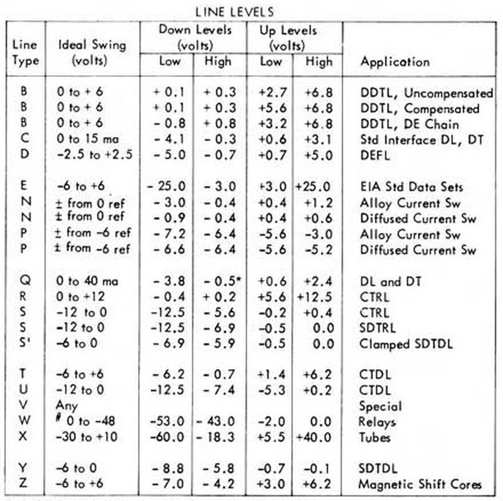
  7. IBM used a remarkable number of different voltage levels for its logic families. The CTDL gates described in this article used the "T" and "U" levels. The table below gives the others.

    IBM's logic families used numerous incompatible voltage levels. From the IBM 1401 Pocket Reference.

    IBM's logic families used numerous incompatible voltage levels. From the IBM 1401 Pocket Reference.


  8. I should point out that having two sets of voltage levels makes debugging the 1401 system very confusing. If you measure -3 volts, for instance, this is a logical low for a T signal and a logical high for a U signal. The wired-OR gates also make debugging inconvenient. If the output is low, you can't easily tell which NAND gate is pulling the output low, and these NAND gates may be on different cards with many different inputs. 

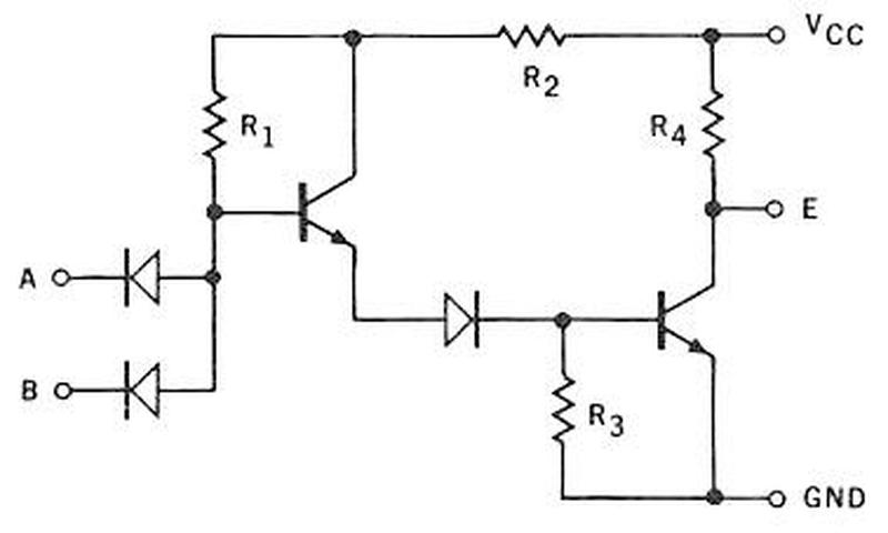
  9. The schematic below shows the implementation of a NAND gate in the Fairchild Micrologic family of integrated circuits. This circuit uses an additional transistor and diode to shift the voltage levels. This was practical in an integrated circuit because the additional components had minimal cost. This circuit wouldn't have worked well in the IBM 1401 because the 1401's germanium components provided a much smaller voltage shift than the silicon components in the Fairchild IC.

    Schematic of a Fairchild Micrologic DTL gate from the databook.

    Schematic of a Fairchild Micrologic DTL gate from the databook.


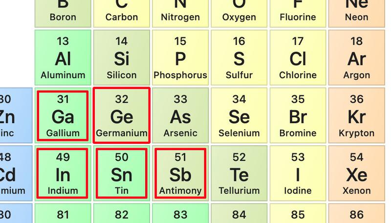
  10. The periodic table shows why elements such as indium were used in the alloy transistors. Note that the semiconductor germanium is in the same column as silicon, which later replaced it. Indium and gallium are in the column to the left, so they have one fewer valence electron. Thus, adding them to the semiconductor makes it more positive (P-type), since electrons are negative. Antimony is to the right; its additional valence electron makes the semiconductor negative (N-type). Tin, in the same column as germanium, was used in the alloy but has no effect on the semiconductor properties.

    This excerpt of the periodic table shows key elements in transistor construction. Source: NCBI.
    This excerpt of the periodic table shows key elements in transistor construction. Source: NCBI.
     

Strange chip: Teardown of a vintage IBM token ring controller

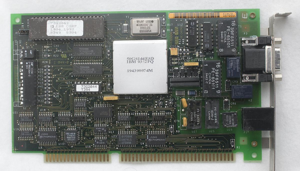
IBM used some unusual techniques in its integrated circuits, and one of the most visible is packaging them in square metal cans. I've been studying these chips recently, since there's not a lot of information about them. I opened up the large metal chip—1.5" on a side—from the token ring network board below. This chip turned out to be stranger and more interesting than I expected, combining analog circuitry, a custom microprocessor, and complex logic. The internal packaging was also unconventional: instead of the bond wires used by most manufacturers to connect the silicon die, IBM used a "flip-chip" technique, soldering the die upside down onto a ceramic substrate. Instead of pads, the chip had solder balls across its surface, giving it an unexpected layout and appearance. In the blog post, I discuss this chip in detail.
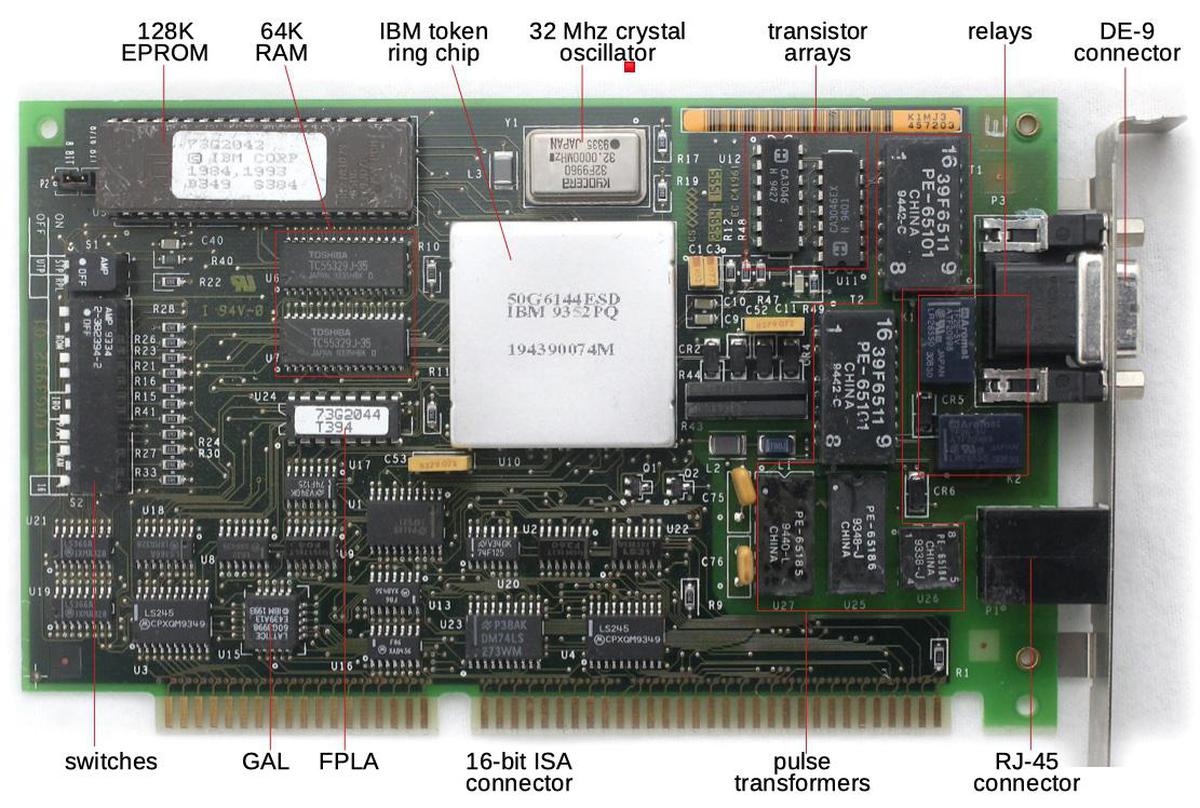
The IBM 4/16 ISA token ring board. Click this photo (or any other) for a larger version.

The IBM 4/16 ISA token ring board. Click this photo (or any other) for a larger version.

The token ring network was introduced by IBM in 1985,1 a local-area network technology that competed with Ethernet and other network systems. In a token ring network, the computers are wired in a ring, with each computer receiving packets from the previous computer and transmitting them to the next computer in the loop. To give a computer access to the network, a special three-byte token circulates in the ring. When a computer receives the token, it can transmit a network packet to the next computer in the ring. The packet travels around the ring until it comes back to the original computer. That computer discards the packet and sends out the token in its place, giving another computer a chance to transmit data. In comparison, an Ethernet network lets computers transmit at any time; if two transmit at the same time, the collision is detected and they try again a bit later. A token ring network had the advantage of avoiding collision, making it more deterministic and fair and providing better performance on a congested network.

IBM's use of square metal cans goes back to the early 1960s with IBM's SLT modules (Solid Logic Technology). Because IBM didn't think integrated circuits were mature enough at the time, they used small hybrid modules with a few transistors, diodes, and resistors mounted on a ceramic substrate. These half-inch-square SLT modules were packaged in an aluminum can for protection, giving IBM circuit boards a unique appearance. In the late 1960s, IBM moved to integrated circuits2 but they kept the ½" metal cans instead of the rectangular ceramic or epoxy packages used by other manufacturers. As integrated circuits required more pins, IBM increased the package size, leading to the bulky 1.5" package that I examined.

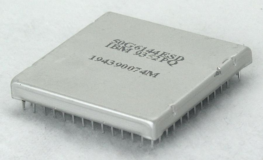
To examine the integrated circuit, I removed it from the board with a hot air gun. In the photo below, you can see the grid of pins underneath the chip. The chip is labeled with the part number is 50G6144. The "ESD" suffix indicates an electrostatic-sensitive device that can be damaged by static electricity and requires special handling. The next line, IBM 9352PQ, is a code for the manufacturing site. The final line, 194390074M, shows that the chip was manufactured in 1994 during the 39th week of the year.

The integrated circuit is packaged in a square aluminum can, 1.5" on a side.

The integrated circuit is packaged in a square aluminum can, 1.5" on a side.

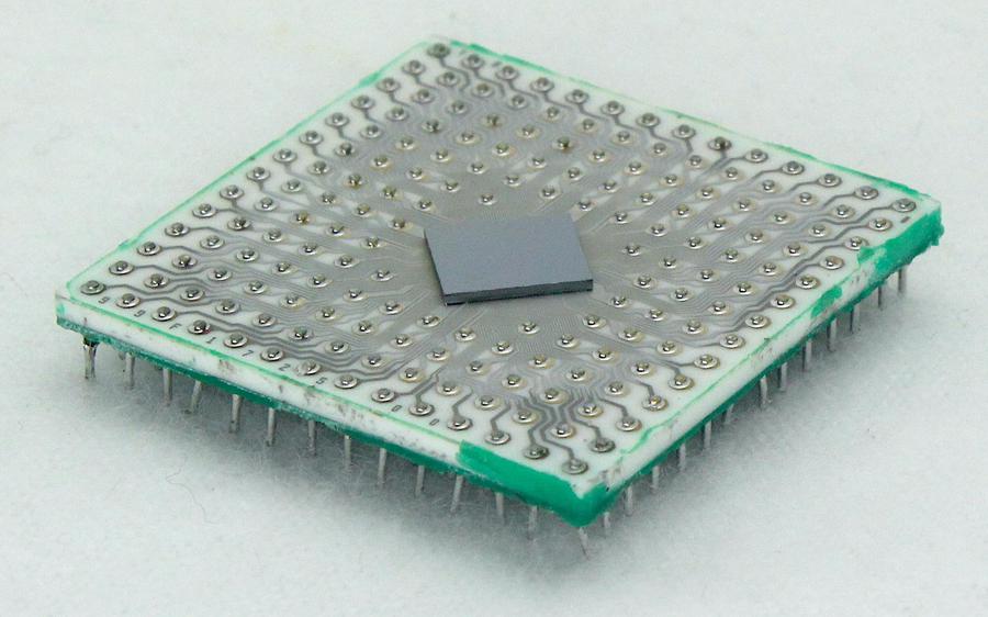
Cutting off the aluminum lid reveals the silicon die inside. The chip is mounted upside down as a flip chip, soldered directly to the connections on the ceramic substrate. Thus, you can't see the chip's circuitry, just the underside of the silicon die. IBM called this mounting technology controlled collapse chip connection or C4.3 (In comparison, most manufacturers mounted a silicon die right side up and connected it to the pins with tiny bond wires.) Tiny printed-circuit traces connect the module's 175 pins to the die.

The integrated circuit with the metal lid removed, showing the silicon die on the ceramic substrate.

The integrated circuit with the metal lid removed, showing the silicon die on the ceramic substrate.

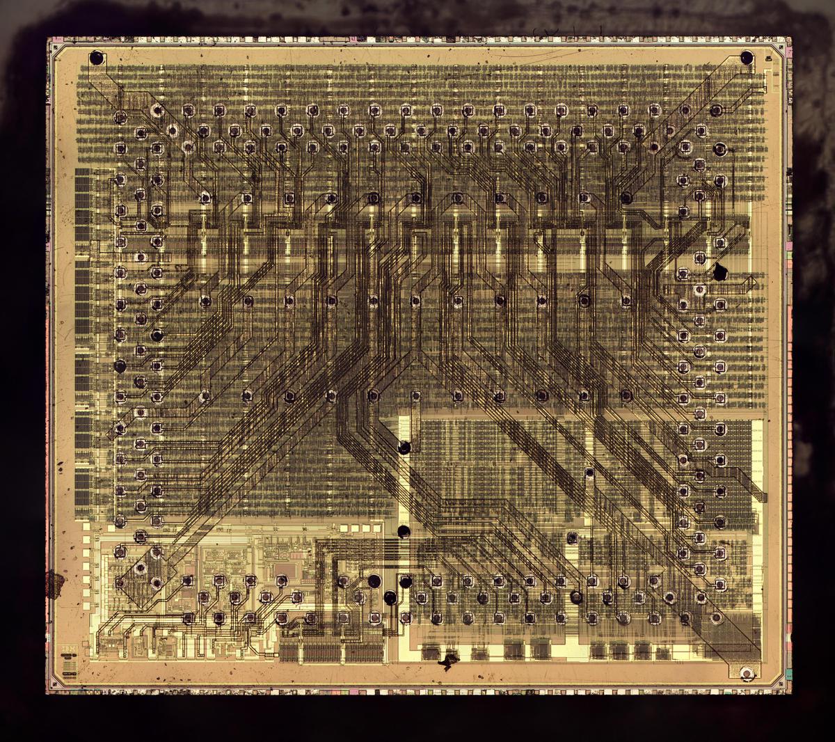
I removed the die from the substrate with the hot-air gun and then dissolved the solder balls with a mixture of hydrogen peroxide and vinegar. By taking numerous photos with a metallurgical microscope, I created the die photo below. The black circles on the die are the positions of the solder balls, more irregular than you might expect. They are not around the edge of the die (as with bond pads), but overlap the circuitry. The chip is fairly large, about 9×7.9 mm, with features of about 1µm. Note the horizontal rows of circuitry; these are standard cells, which I will discuss below.

Die photo of the chip. Click this (or any other) image for a larger version.

Die photo of the chip. Click this (or any other) image for a larger version.

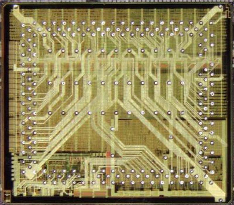
The pattern of solder balls is more visible in Antoine Bercovici's photo below. There are rows three-deep of solder balls along the four sides, as well as rows through the middle of the chip and more in the corners. Roughly speaking, the solder balls around the edges are for signals, while the solder balls in the middle distribute power and ground. Note the tangled metal wiring on top of the chip that connects the solder balls to the underlying circuitry.4

Die photo showing the solder balls and upper metal clearly. Courtesy of Antoine Bercovici.

Die photo showing the solder balls and upper metal clearly. Courtesy of Antoine Bercovici.

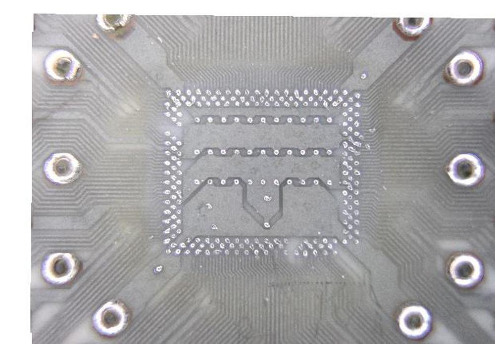
The photo below shows a closeup of the ceramic substrate that holds the die; compare the pattern to the die above.5 The die was soldered to the rectangular array of contacts in the middle, while the large circles around the edge of the photo are the pins of the chip. Note the dense, complex wiring pattern between the pins and the tiny contacts. The wiring traces are extremely thin (about 30µm), with thicker traces from power and ground. The contacts form a complex pattern. most are in a rectangular array, three deep. However, there are also rows of contacts through the center of the chip, connected alternately to power and ground by the thick traces inside the rectangle, and a few scattered contacts. The contact pattern on the substrate was optimized for the layout of this particular chip. Power distribution was a particular concern.

A closeup of the ceramic substrate showing where the die is mounted.

A closeup of the ceramic substrate showing where the die is mounted.

It's interesting to consider the hierarchy of connections between the coarse 0.1" grid of the chip's pins and the tiny 1µm features on the chip. At the top level, the pin spacing is 0.1" in a 14×14 grid. The solder balls have a spacing of 0.01", so the ceramic substrate reduces the spacing by a factor of 10. The solder balls are connected to the wiring on top of the die, spaced at 0.001", increasing the density by another factor of 10. The top wiring is connected to the underlying wiring on the chip, with a spacing of 0.0001", another factor of 10. Finally, the feature size on the die is about 1µm, another factor of 2.

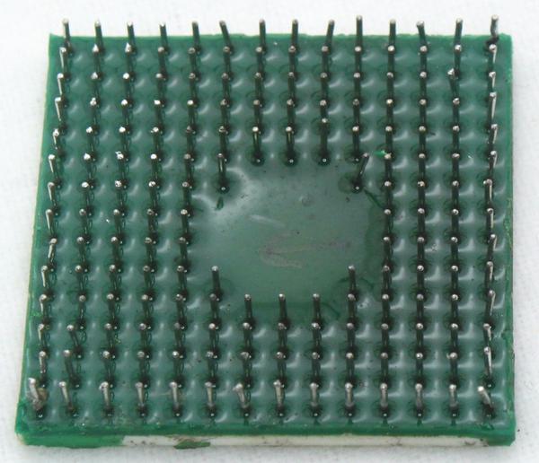
With this type of packaging, you can visualize the die position by looking at the underside of the IC (below). Because the chip is soldered directly to the substrate, there are no pins where the chip is attached. Thus, the spot with no pins indicates the position of the die.

Underside of the package.

Underside of the package.

Inside the chip

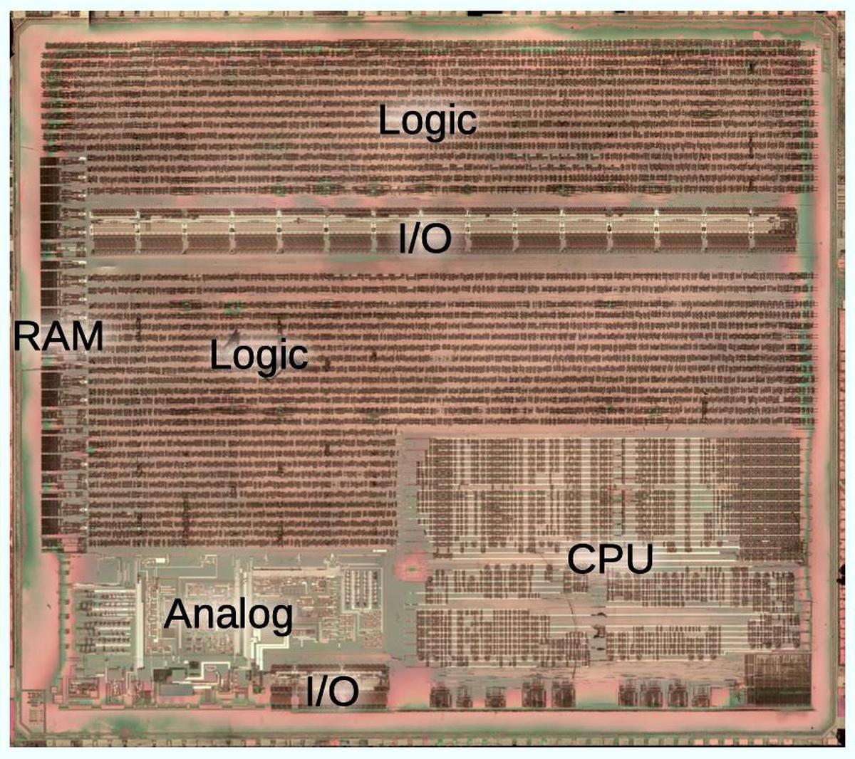
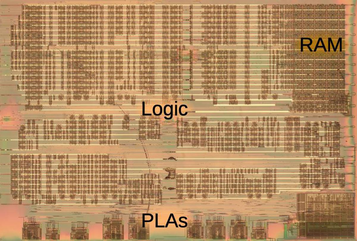
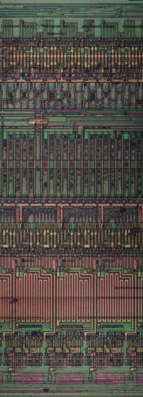
The die photo below shows the chip with most of the metal layers dissolved, making the transistor structure underneath visible. The chip has three main components: a 16-bit microprocessor CPU, an analog front end for the network signals, and 24,000 logic gates for the main functionality. The chip also has some buffer RAM at the left, and I/O drivers in the middle and bottom. (IBM originally implemented the token ring interface with six analog and digital chips. To decrease cost, they put all the functionality onto a single chip, resulting in the combination of analog and digital circuitry.)

The die with major components labeled. The metal layer has been removed to show the circuitry underneath.

The die with major components labeled. The metal layer has been removed to show the circuitry underneath.

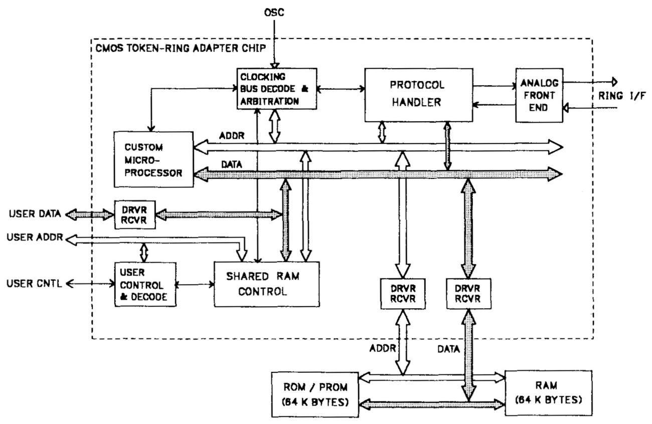
The block diagram below shows the complex functionality of the chip. Starting in the upper right, the analog front end circuitry communicates with the ring. The analog front end extracts the clock and data from the network signals. The protocol handler implements the low-level token ring protocol: it decodes data, breaks packets into frames and performs error checking. Network data is moved between on-chip buffers and the external RAM by the shared RAM control. Finally, a custom 16-bit microprocessor implements the data link layer protocols and controls the chip.

Block diagram of the chip, from IBM's paper.

Block diagram of the chip, from IBM's paper.

Standard-cell logic

The chip's logic is implemented with a CMOS standard cell library and consists of about 24,000 gates. The idea of standard-cell logic is that each function (such as a NAND gate or latch) has a standard layout. These cells can then be combined by automated design tools to create the desired logic. (This is in contrast to older methodologies, where the designer would lay out each transistor individually, either on paper or using design software.) Standard cells make chip design much easier, since software can do the circuit synthesis, layout, and routing, However, the design isn't as flexible or optimized as a fully-custom circuit.

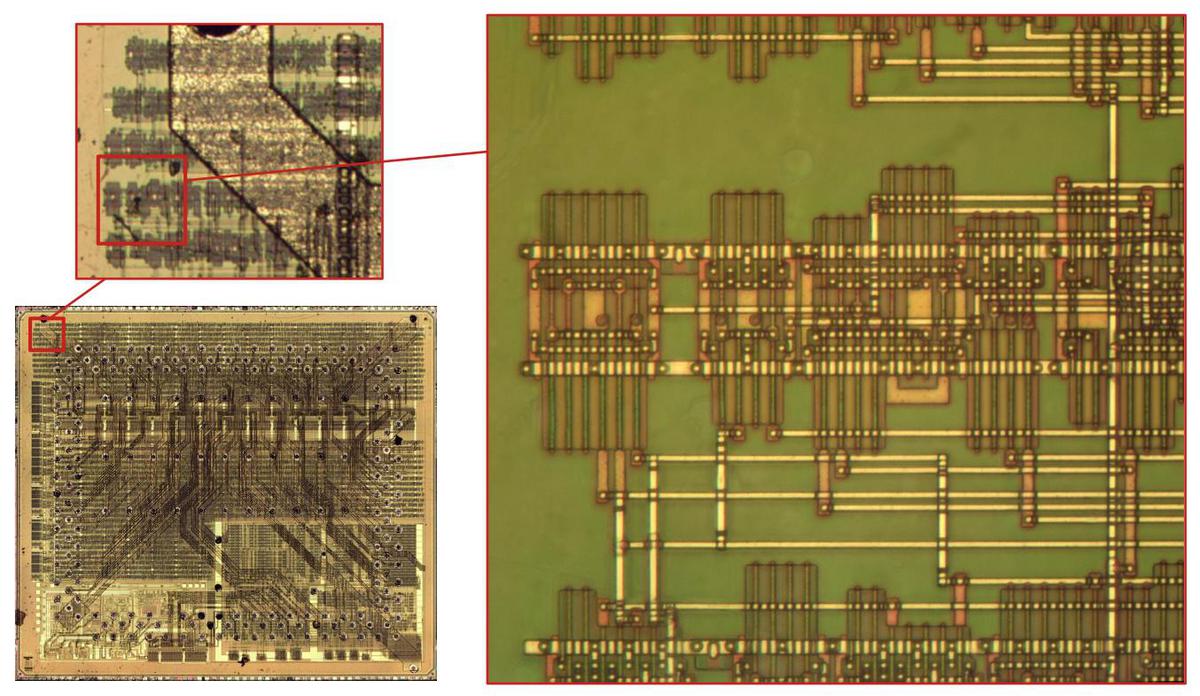
The standard cell layout is visible on the chip, with the cells arranged in uniform rows, connected by horizontal and vertical wiring. The diagram below magnifies the die to zoom in on five rows of standard-cell logic, and then a single row, to show how small the cells are on the die.

Zooming in on the die shows rows of standard cell logic. Another zoom shows the details of the logic.

Zooming in on the die shows rows of standard cell logic. Another zoom shows the details of the logic.

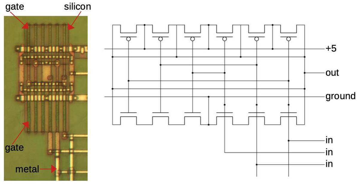
The standard cell below implements a 3-input NAND gate, and I'll explain how it is constructed.6 There are 6 PMOS transistors on top and 6 NMOS transistors on the bottom. The transistors are formed from a region of doped silicon at the top and another at the bottom. Vertical lines of polysilicon, a special type of silicon, form the transistor gates. Polysilicon is also used for vertical wiring inside the cell. The chip has three layers of metal: the bottom layer is used for horizontal wiring, the middle layer is used for vertical wiring, and the top layer connects to the solder balls. Horizontal metal wiring connects the transistors inside the cell and connects the cell to other cells. The two thick horizontal metal wires provide power and ground for the cell. The second, vertical metal layer provides vertical wiring across and between cells. This layer also implements the power connections between the solder balls and the horizontal power wiring visible here. The round dots are connections between layers (silicon, polysilicon, or metal). The schematic on the right matches the layout of the cell.

Closeup of a cell that implements a NAND gate.

Closeup of a cell that implements a NAND gate.

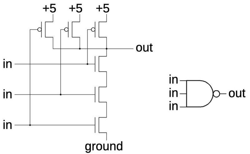
In the schematic below, I've removed the redundant transistors and rearranged the layout to make the NAND circuit more clear. If all inputs are 1, the NMOS transistors at the bottom turn on, pulling the output low. If any input is 0, a PMOS transistor turns on, pulling the output high. Thus, the circuit implements a NAND gate.

Schematic of the 3-input NAND gate.

Schematic of the 3-input NAND gate.

To summarize, standard-cell logic provides a convenient, automated way of implementing logic. A small number of standardized cells implement the basic logic functions. These cells are arranged in rows and wired together to create the desired logic. (From the teardown perspective, standard-cell logic is somewhat disappointing, since the high-level structure is not visible; it's just a bunch of uniform cells.)

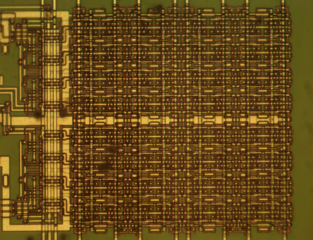
The logic circuitry includes some static RAM buffers to hold network data. These were custom-implemented (as were the I/O drivers) instead of using standard cells. The photo below shows a block of RAM cells.

One of the RAM buffers on the chip.

One of the RAM buffers on the chip.

Inside the CPU

The chip contains a 16-bit CMOS control microprocessor that was custom-designed by IBM7 and contains about 10,000 gates. This processor handles the network protocol, controls transmit and receive operations, and manages the shared memory. It runs at 5.34 megahertz and performs about 3 MIPS (million instructions per second). The microprocessor runs code from an EPROM on the board. IBM calls this "microcode", but it's unclear if this is microcode in the usual sense or just firmware instructions.

The CPU, with main functional blocks labeled. The metal layer has been removed.

The CPU, with main functional blocks labeled. The metal layer has been removed.

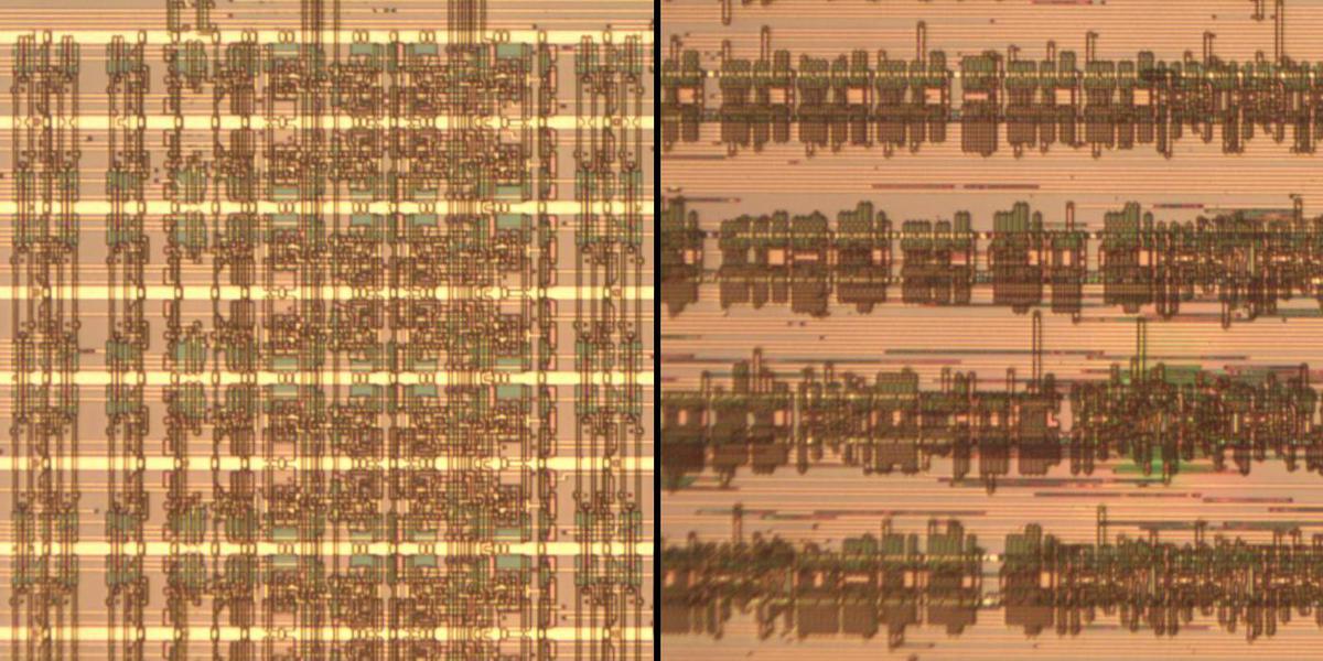
The CPU is built with standard-cell logic (except for the RAM and ALU), but curiously the cell layout is entirely different from the rest of the chip, presumably because it had different designers. The photo below compares the CPU's logic (left) with the other logic (right). The CPU fits 7 rows of logic in the same vertical space that holds 4 rows of the regular logic. On the other hand, the logic on the right appears to be much dense horizontally.

Comparison of the CPU's standard-cell logic (left) with the rest of the chip (right), at the same scale.

Comparison of the CPU's standard-cell logic (left) with the rest of the chip (right), at the same scale.

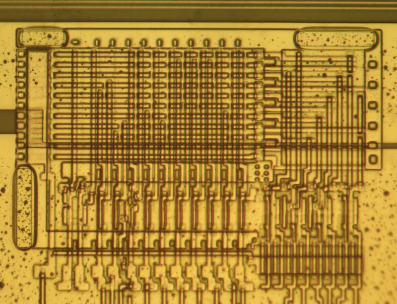
One design feature of the CPU that's visible on the die is its use of multiple PLAs (programmable logic arrays) for instruction decode and control. (Looking at the photo, I count nine small PLAs and a large PLA in the corner.) A PLA provides a structured and dense way of implementing logic (typically AND-OR logic). More importantly, PLAs also provided flexibility and the ability to easily change the design. In the PLA below, 12 signals enter at the lower left. The matrix above converts these to 11 signals that pass to the right. The second matrix generates 8 outputs. The contents of the PLA are visible as the pattern in the metal layer. Since the PLA could be modified by changing the chip's metal layer, bug fixes could even be done after the silicon had been etched.

One of the many PLAs in the CPU.

One of the many PLAs in the CPU.

The CPU contains memory cells for register storage (which they call a 16×16 cache). This RAM design is different from the RAM design in the logic circuitry.

Memory cells in the CPU.

Memory cells in the CPU.

Analog circuitry

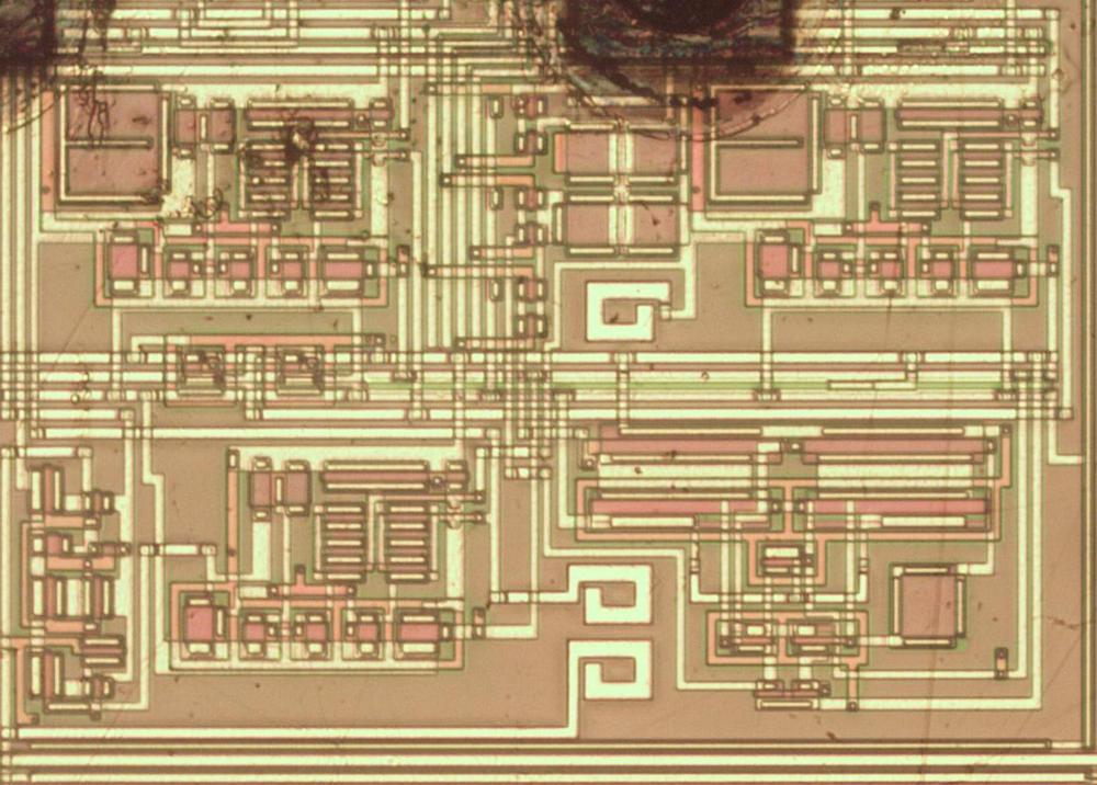
The chip contains a block of analog circuitry implemented in CMOS. This circuitry "performs signal conversion and clock recovery functions as well as detecting and compensating for line impairments". This circuitry includes resistors, capacitors, MOS transistors with special properties, and other components.8 The analog block uses a variety of circuits such as op-amps, switched-capacitor amplifiers, voltage references, peak detectors, a charge pump, voltage-controlled-oscillator, and phase-locked loop.

Die photo showing part of the analog circuitry.

Die photo showing part of the analog circuitry.

One challenge in the design was to minimize "jitter" in the clock signal extracted from the network data. Because each node retransmitted the data, jitter would accumulate as a packet traversed the ring, so each node had to be accurate. They used a variety of techniques to keep noise out of the signal such as providing separate power and ground for the analog circuitry, using differential signals in the circuitry, and keeping logic signals away from the analog circuitry.

The analog circuitry made the chip much more complex to manufacture and test.9 The capacitors and special transistors required special process steps during manufacturing. Manufacturing tolerances were also much tighter since process variations could change the electrical characteristics enough to make the analog circuitry stop performing. Some of the analog circuitry was too sensitive to be tested on the wafer and couldn't be tested until the chip was packaged, making failed chips much more costly. Even so, IBM found it worthwhile to put the analog circuitry on the chip.

Shrinking the chip

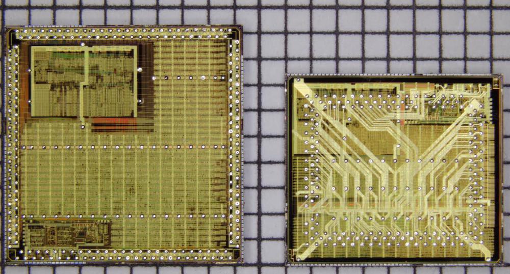
IBM originally made the token ring chip in 1988. The chip I examined is a smaller version from 1994. The photo below compares the two chips on a 1 mm grid; the older, larger chip is on the left. Note that both chips have the same microprocessor block (upper left corner) and the same analog block (lower left / upper right corner). The height of the standard cell logic rows is much smaller in the newer chip, probably how they shrunk the logic. The solder balls on the left connect to the underlying circuitry, while the solder balls on the right are routed all over the chip by a third layer of metal.

Comparison of the two chips. Photo courtesy of Antoine Bercovici.

Comparison of the two chips. Photo courtesy of Antoine Bercovici.

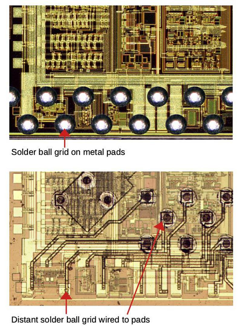
The analog section from the old chip was copied to the new chip unchanged, but the connections to solder balls are very different, showing the change in wiring techniques. In the old chip (left), the solder balls are on top of metal pads that are connected to the circuitry. The layout is similar to integrated circuits that use wire bonding and bond pads. In the old chip (right), the solder ball grid is not anchored to the underlying chip architecture, but follows its own constraints. A new layer of metal connects the solder balls to the pads. The pads remain in their atavistic positions, despite being unused in the new chip.

Comparison of the analog section of the old chip and the new chip. The color of the chips is different due to lighting.

Comparison of the analog section of the old chip and the new chip. The color of the chips is different due to lighting.

The token ring board

I'll just say a bit about the token ring board that contains this chip. The board is an ISA card from 1994. The IBM chip dominates the board, but there are also numerous other chips, largely 74F-series TTL. There's also a square (and curiously thick) Lattice chip, probably a GAL (Generic Array Logic). A GAL is a programmable logic chip, combining AND/OR logic with flip-flops. A Signetics chip with an IBM label on top is probably a field-programmable logic array (FPLA). Despite all the complexity of the IBM chip, the board requires a lot of programmable logic and simple logic ICs, mostly to interface to the computer's ISA bus. The board has 64 kilobytes of RAM to store network data, two Toshiba TC55329 32K×9 bit static RAM chips. This RAM is accessible both by the network card and by the host PC. The code for the internal microprocessor is contained in an EPROM chip on the board, an AMD 27C1024 chip holding 128 kilobytes as 16-bit words. The EPROM chip has an adhesive label on it with the IBM part number 73G2042, indicating the microcode version.

The token ring board plugs into a PC's ISA slot.

The token ring board plugs into a PC's ISA slot.

The right side of the board holds the analog circuitry to interface with the network. Five pulse transformers provide electrical isolation between the interface board and the potentially-dangerous voltages of the network. Two bypass relays disconnect the card from the ring when not in use, preserving the ring's connectivity. There are also two transistor arrays along with resistors and capacitors to condition the network signals before passing them to the token ring chip. The card connects to the network via an RJ-45 connector that can be used with unshielded twisted-pair (UTP) cable. It also has a DB-9 connector on the back that can be used with shielded twisted-pair (STP).11

In the 1980s, many different local area networking standards were competing including Ethernet, Token Ring, Datapoint's ARCnet, Apple's LocalTalk, Omninet, and Econet. By the early 1990s, Ethernet won due to a combination of factors: much lower cost (about 1/5 the cost of Token Ring), less complexity leading to faster technological improvement (such as 100 Mb/s Ethernet and switched Ethernet), and a wider ecosystem than IBM provided.10 The complexity of the chip reflects the complexity of Token Ring and illustrates that IBM's technological edge in the 1980s was a double-edged sword: although it initially gave Token Ring a large performance advantage, the simpler technology of Ethernet eventually won.12

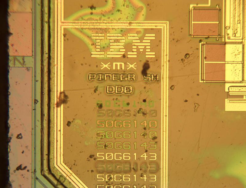
The IBM logo is in the lower-left corner of the die, along with the mysterious codename "PINEGR SH".

The IBM logo is in the lower-left corner of the die, along with the mysterious codename "PINEGR SH".

Thanks to Antoine Bercovici for die photos and information. Thanks to my Twitter readers for discussion. I announce my latest blog posts on Twitter, so follow me @kenshirriff. I also have an RSS feed.

Notes and references

  1. IBM's token ring network was inspired by ring network research from the 1970s, such as the Cambridge Ring

  2. IBM called their integrated circuits MST, Monolithic System Technology. 

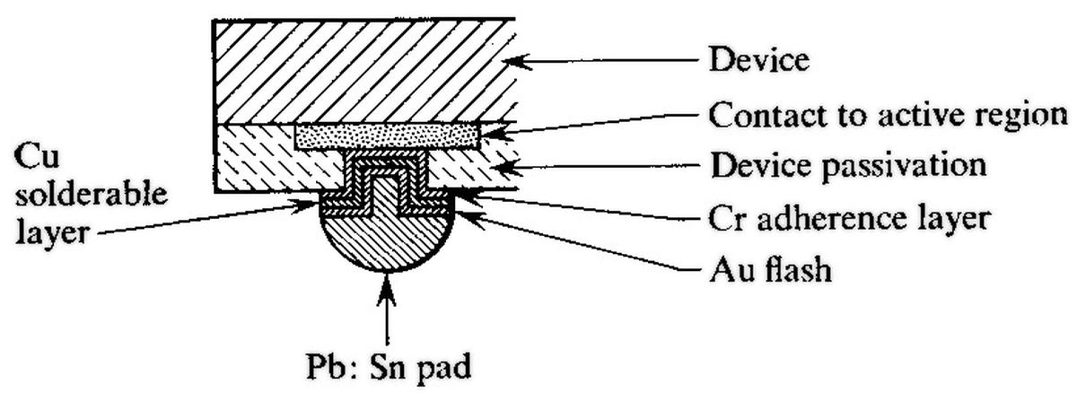
  3. The diagram below illustrates the complex construction of a solder ball on the die. Thin layers of aluminum, chromium, copper, and gold are put on the silicon to obtain the necessary properties, followed by a layer of lead-tin solder, which is reflowed to form the balls. The chromium bonds to the oxide layer, while the copper provides solderability and the gold protects the copper from oxidizing.

    Diagram of a solder pad, from this paper.

    Diagram of a solder pad, from this paper.


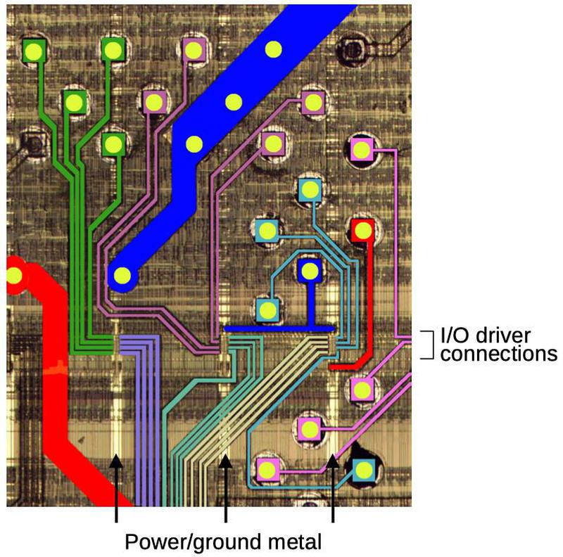
  4. The metal wiring on the top layer of the chip looks like a mess, but there is some structure behind it. The diagram below shows a small section of this wiring, colored to show the structure. The solder balls are shown in yellow. The red and blue traces transmit power and ground from the solder balls across the chip. These traces connect with the vertical strips of metal wiring that transmit power and ground throughout the chip. The other wiring connects the signal solder balls to the I/O drivers, converging in a narrow band in groups of four. Most of the solder balls are positioned with little regard for the underlying circuitry; the top metal layer provides the "glue" between them and the integrated circuit itself. The result is the peculiar metal pattern visible on top of the chip.

    The colored lines show how the top layer of metal wiring connects the solder balls to the chip.

    The colored lines show how the top layer of metal wiring connects the solder balls to the chip.

    In most integrated circuits, the I/O drivers are around the edges of the chip next to the bond pads. However, in this chip, most of the I/O drivers stretch in a line across the middle of the chip (indicated above). More I/O drivers are at the bottom of the chip next to the CPU, probably connected to it directly.

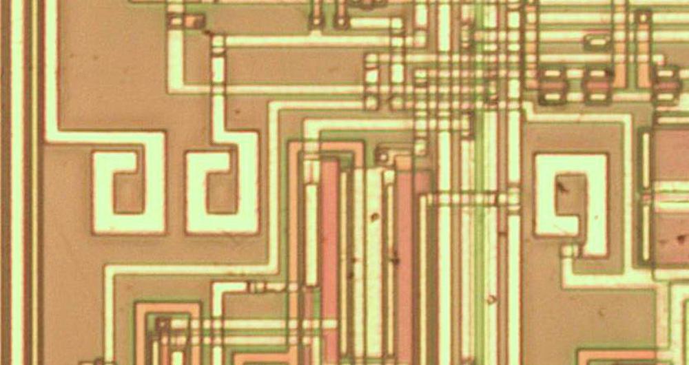
    The photo below shows three I/O drivers, side by side. The metal layers have been mostly removed to reveal the silicon underneath. These drivers are fairly complex. The top half contains large drive transistors to provide relatively high-current outputs, along with smaller control transistors. The lower half contains reddish serpentine resistors made out of polysilicon. These resistors help protect the sensitive gates of the input transistors from static discharges. For output pins, these resistors are disconnected. The middle resistor, however, is connected to the input transistor near the bottom.

    Die photo of three I/O drivers.

    Die photo of three I/O drivers.


  5. The die is flipped over when soldered to the substrate. This needs to be kept in mind when comparing the die and the substrate. For instance, the two extra power connections for the CPU are in the lower right of the die but the lower left of the substrate. (Just a note to avoid potential confusion.) 

  6. I'm not sure which transistors are NMOS and which are PMOS in the gate. I'm assuming the PMOS are on top and it's a NAND gate, but it could be the other way around, in which case it's a NOR gate. 

  7. The processor is described as using IBM's "universal controller (UC) architecture" but there's very little information about this architecture. Wikipedia claims this architecture consisted of UC0 (8-bit), UC.5 (16-bit), and U1 (32-bit), with upwards compatibility. An alt.folklore.computers thread and this page provide a bit more information. 

  8. The analog circuitry contains small loops of various sizes that I was unable to identify. They are only connected on one end and have nothing underneath, so they don't seem to be inductors. Twitter readers suggested probe points, disconnected circuitry, or reflective delay lines, but their function remains unclear.

    Three of the loops on the die.

    Three of the loops on the die.


  9. The designers were very proud of the testability of the chip, writing a paper about the testing methodology, and a second paper about testing the analog circuitry. The chip includes a boundary scan feature (kind of like JTAG) and built-in self-test features, as well as mechanisms to isolate the analog block and the CPU for separate testing. 

  10. Much of the information about this chip comes from A 16-Mbit/s adapter chip for the IBM token-ring local area network. That article describes an earlier version of the chip, so I can't be sure everything is accurate when applied to this chip. (It appears to me that the chips are the same apart from the smaller size of the newer chip.) One source says the two chips are compatible. The older chip has part number 51F1439 while the chip I examined is 50G6144.

    For information on Token Ring, the book The Triumph of Ethernet: Technological Communities and the Battle for the LAN Standard discusses the competition between network protocols in great detail. You might also like Foone's Twitter thread on Token Ring. Interestingly, one of the original "ENIAC Women", Jean Bartik, wrote a 1984 article on Token Rings—"IBM's Token Ring: Have the Pieces Finally Come Together?"—but unfortunately I haven't been able to locate a copy. 

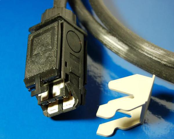
  11. Token Ring cables could be joined using the "IBM Data Connector", a curious type of connector. The connectors are known as hermaphroditic because two connectors can be joined without worrying about male and female ends. The connectors were nicknamed "Boy George" connectors after the androgynous singer, which seems questionable by current standards. (The nickname may also be motivated by the BOGR text on the connector, which I think indicates the black, orange, green, and red wires.)

    IBM Data Connector. Photo from Redgrittybrick, (CC BY-SA 3.0).

    IBM Data Connector. Photo from Redgrittybrick, (CC BY-SA 3.0).


  12. The book The Innovator's Dilemma describes how a low-end but innovating technology can defeat an advanced, entrenched technology. I haven't investigated Token Ring versus Ethernet enough to be sure this model applies, so consider it a hypothesis. 

Booting the IBM 1401: How a 1959 punch-card computer loads a program

How do you boot a computer from punch cards when the computer has no operating system and no ROM? To make things worse, this computer requires special metadata called "word marks" that can't be represented on a card. In this blog post, I describe the interesting hardware and software techniques used in the vintage IBM 1401 computer to load software from a deck of punch cards. (Among other things, half of each card contains loader code that runs as each card is read.) I go through some IBM 1401 machine code in detail, which illustrates the strangeness of the 1401's architecture and instruction set compared to a modern machine.

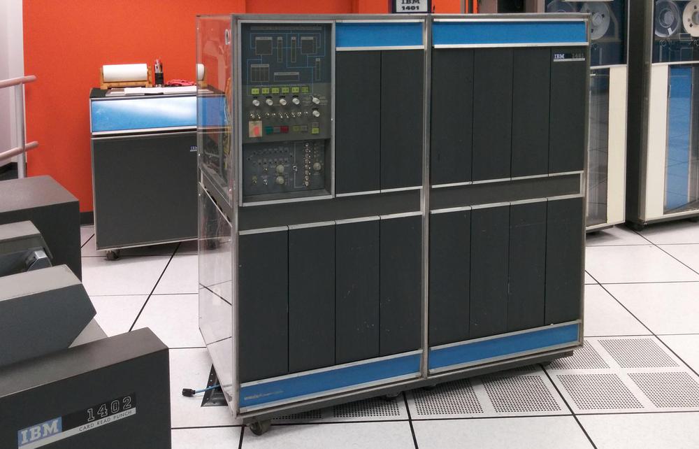
The IBM 1401 was an early all-transistorized computer, so early that it didn't use silicon transistors but germanium transistors. It was announced in 1959, and went on to become the best-selling computer of the mid-1960s, with more than 10,000 systems in use. The 1401 leased for $2500 a month (about $20,000 in current dollars), a low price that opened up computing to many companies. Even a medium-sized business could use the 1401 for payroll, accounting, inventory, order processing, and invoicing.

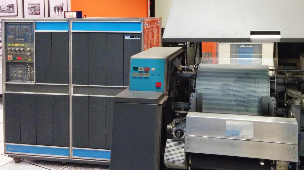
An IBM 1401 mainframe computer at the Computer History Museum. IBM 729 tape drives are at the right.

An IBM 1401 mainframe computer at the Computer History Museum. IBM 729 tape drives are at the right.

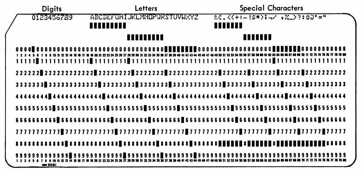
To understand the 1401's architecture, it helps to understand how punch cards were used in that era. In 1928, IBM developed the 80-column punch card that became the standard for data processing for decades. A punch card held 80 characters, one per column, with the character represented by the holes punched in that column, as shown below. The 6-bit character set was limited to 64 different characters: upper case letters, numbers, and some special characters. Instead of binary, cards used a BCD-based encoding (which later was extended to create EBCDIC).1

Punch card code, from IBM 29 Card Punch Reference Manual.

Punch card code, from IBM 29 Card Punch Reference Manual.

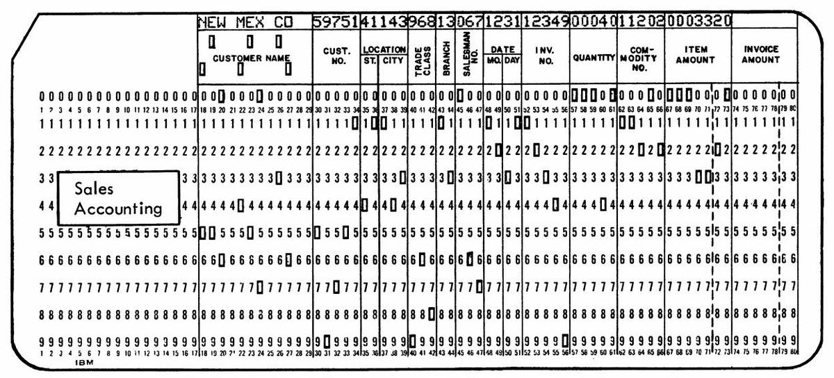
Despite their limitations, punch cards were extensively used for data processing into the 1970s and beyond. A typical application used one card for each data record, so everything needed to fit into 80 columns2 which were divided up into fixed-length fields. Often, custom cards would be printed that showed the fields for an application, such as the card below designed for accounting.3 Each field has a fixed location. For instance, in the card below, the customer name is from columns 18 to 29 while the invoice amount is in columns 74 through 80.

Example card, from IBM 29 Card Punch Reference Manual.

The IBM 1401 has a peculiar architecture, optimized to support these punch-card applications. The idea is that fixed-length fields were be delimited in memory by word marks, a sort of metadata, and then instructions operated on these arbitrary-length fields. This let you move a 19-character name string with a single instruction. Or you could perform arithmetic on a 50-digit numeric field with a single instruction. Thus, word marks were convenient for fixed-field data, since you didn't need to loop over each character of the field.

To implement word marks, each memory location had 6 bits to hold a character as well as a separate bit to hold the word mark. (These were not bytes, as the IBM 1401 predated the popularity of byte-based computers.) It's important to note that the word marks were independent of the characters. Word marks were set or cleared using different instructions from the ones that acted on characters. Once word marks were configured, they remained unchanged as data records were read into memory.

Word marks were also critical for machine instructions since they indicated the length of the instruction. A machine instruction in the 1401 consisted of one to eight characters. The first character was the op code, potentially followed by addresses and/or a modifier. Each instruction needed to have a word mark set on the op code and a word mark on the next character after the instruction (i.e. the op code of the next instruction). Note that word marks create a problem. The machine instructions of a program are directly represented as characters on a punch card, but a punch card cannot hold the necessary word marks.

Thus, loading a program into the 1401 raised two problems. First was the standard computer bootstrap problem: if there's no program in the machine, what performs the load? But there was a second: word marks are a key component of 1401 machine code, but word marks cannot be represented on punch cards. In the next section, I'll explain in detail how the IBM 1401 solved these problems.

Loading a program

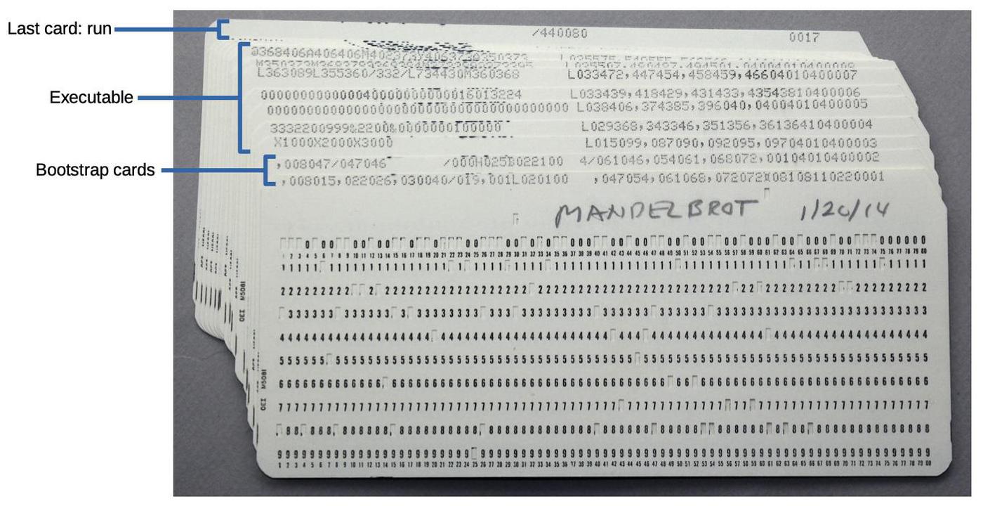
To load a program, a card deck, such as the short one below is placed into the card reader. Each card has the contents of the card printed at the top, with the holes punched in the columns below. The first two cards are bootstrap cards that initialize the computer's memory, clearing it out and setting necessary word marks. The bulk of the cards hold the machine code of the desired program on the left, and the machine code of the loader on the right. The last card runs the program.

A card deck for my Mandelbrot program.

A card deck for my Mandelbrot program.

At the far right of each card, columns 72-75 hold a sequence number (0001 through 0017). If you dropped a card deck, the cards could be put back into order by a card sorter, sorting on the sequence number.8

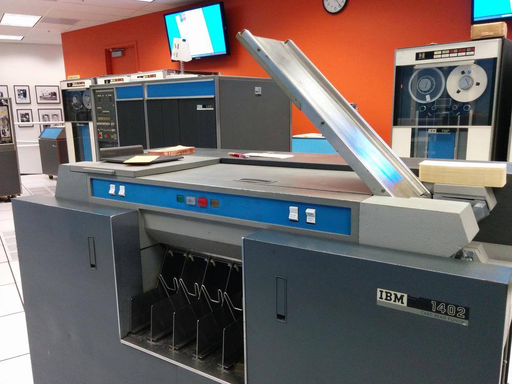
The load process was started by pressing the "Load" button on the card reader (the orange button near the center of the blue panel). This button causes several actions to take place.4 The first card was read, and the contents are placed in memory addresses 1 through 80. A word mark was set on address 1, and cleared from addresses 2 through 80. Finally, the instruction at address 1 was executed. Remember that these operations were implemented in hardware by boards with discrete transistors; there's no microcode or operating system to help out with these tasks.5

The IBM 1402 card reader/punch. The 1401 computer is in the background (left) and a tape drive is at the right.

The IBM 1402 card reader/punch. The 1401 computer is in the background (left) and a tape drive is at the right.

Bootstrap card 1

The first card contains the machine code:

,008015,022026,030040/019,001L020100   ,047054,061068,072072⌑08108110220001

The first instruction ,008015 is "Set Word Mark", a critical part of the bootstrap sequence. The comma is the op code and the address arguments are "008" and "015". (Since the 1401 is a decimal computer, not binary, the characters "015" are the same as the address 15.) This instruction sets word marks at the specified addresses, 8 and 15.

Remember that an instruction needs to have a word mark on the opcode and a second word mark on the character following the instruction. The "Load" button put a word mark at address 1, but what about the second word mark? It turns out that the hardware has an exception for the "Set Word Mark" instruction 6 allowing it to execute without the second word mark. (This exception is crucial, since otherwise the first instruction can't execute. Was this carefully planned or a hack to make things work? I don't know.)

The word marks that were set by the first instruction let the next two instructions run. They are also "Set Word Mark" instruction, putting word marks at addresses 22, 26, 30, and 40. Note that each "Set Word Mark" instruction sets two word marks but only "uses up" one, so the code is making progress, preparing word marks for future instructions.

Now we come to /019; with the slash opcode indicating the somewhat curious "Clear Storage" instruction. This instruction starts clearing storage at the specified address (19) and proceeds downwards until the address is a multiple of 100. Thus, in this case it will clear from address 19 down to address 0, erasing both characters and word marks. (These locations contained the instructions we just executed.) A location is erased by storing a blank; this may seem like a strange choice, but keep in mind that an empty punch card column is read as a blank. The next Set Word Mark instruction, ,001 puts a word mark back at location 1.

At this point, the contents of memory are as shown below. Word marks are indicated by underlined characters, which is how the IBM documentation indicated word marks.

                   40/019,001L020100   ,047054,061068,072072⌑08108110220001

The next instruction is L020100 "Load Characters to a Word Mark". This instruction copies the character at address 20 (i.e. "4") to address 100. The instruction then continues copying downwards (copying the blanks) until it hits a word mark (which is at address 1). To summarize, addresses 20 through 1 are copied to addresses 100 through 81. Locations 81 through 99 received blanks, while address 100 received a "4". This may seem pointless, but the "4" will turn out to be an important indicator shortly. This instruction also illustrates how word marks allow a long field to be copied with a single instruction.

The next three instructions set word marks at addresses 47, 54, 61, 68, and 72. (The boot code needs to go to a lot of effort to ensure that word marks are set up for future instructions.) The next instruction ⌑081081 has IBM's unusual "lozenge" character as the opcode. This instruction clears the word mark at address 81 (which had been copied from address 1). The final instruction on the card, 1022, reads the next card (opcode 1 is "Read") and then jumps to address 22. A lot has taken place to execute one card, but the next card has some remarkably tricky code.

Bootstrap card 2

After reading the second bootstrap card, memory locations 1 through 80 hold the data:

,008047/047046       /000H025B022100  4/061046,054061,068072,00104010400002

Execution of this card starts at address 22 with the Clear Storage instruction /000. Remember how the Clear Storage instruction proceeds downwards until the address is a multiple of 100? In this case, it will clear address 0 and then immediately stop on address 0 (a multiple of 100). However, a register called the B register will hold the next address (counting downwards), which will wrap from 0 to the top address in memory. For simplicity, I'll assume the code is running on a 1401 model with 1,000 characters of memory so the B register will hold the address 999.7

The next instruction H025 is a tricky bit of self-modifying code. It stores the contents of the B address register into locations 23-25, changing the "Clear Storage" instruction that we just executed to /999. Next, the B022100 4 instruction will branch to address 22 if address 100 holds a "4" (which is true because the first card put a "4" there.)

Back at address 22, the Clear Storage instruction was modified to be /999, so it will now clear addresses 999-900. It is followed by H025, which, as before will store the B register into the Clear Storage instruction. This time it will modify the Clear Storage to start at 899. Finally, the conditional branch loops back to address 22 as before.

The result is that this loop clears memory 100 characters at a time, using self-modifying code to update the position. This loop continues until addresses 100-199 are cleared. At this point, the branch instruction will fail because address 100 holds a blank and not a "4". At this point, the loop has cleared all of storage from 100 to the end of memory, erasing characters as well as any word marks.

The next instruction is Clear Storage /061046 which clears storage from address 46 down to 0 and then branches to 61. At address 61, ,001040 sets word marks at addresses 1 and 40. Finally, 1040 reads the next card and starts execution at address 40. As with the first card, columns 1 through 80 of the card are read into memory addresses 1 through 80.

The program cards

The next phase consists of reading the desired program into memory. A typical card is:

3332200999&2200&0000000100000          L029368,343346,351356,36136410400004

The left part of the card (columns 1-29) contains machine code for the program that we want to run. The right part (columns 41-71) contains the loader code that will execute card-by-card, loading that code into the right part of memory and setting word marks.

The first loader instruction L029368 copies the program code from the card reader buffer into the desired memory locations. Specifically, it will copy starting from address 29 down to the word mark at address 1. These characters will be copied into addresses 368 down to 340. The next instructions set the word marks in this code, at addresses 343, 346, 351, 356, 361, and 364. This answers the question of how the program in memory gets word marks even though punch cards can't explicitly store word marks. Finally, 1040 reads the next card and starts executing it at address 40.

The following cards have the same structure: the program on the left and the loader code on the right. Interestingly, the number of characters of program code is variable because the loader code can set at most 6 word marks per card. In the worst case, all the characters need word marks so only 6 characters can be provided by the card. In the best case, 40 characters can fit on the left side of the card.

The run card

The last card has the Clear Storage instruction /333080. This clears memory from address 80 downwards to 0, wiping out the card buffer and the loader code so the program will start with a clean slate. The Clear Storage instruction then jumps to address 333, starting the execution of the program. After all this work, the computer finally runs the program we wanted to run. While the loading process seems very long when written out, the card reader is fast for an electromechanical device, with over 13 cards per second zipping through it.

The program I used in the example is a Mandelbrot fractal generator that I wrote. The photo below shows the results of the program, which took 12 minutes to execute. I discuss the program in detail in this post.

The IBM 1401 mainframe computer (left) at the Computer History Museum printing the Mandelbrot fractal on the 1403 line printer (right).

The IBM 1401 mainframe computer (left) at the Computer History Museum printing the Mandelbrot fractal on the 1403 line printer (right).

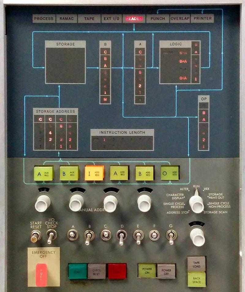
The bootstrap code I described above is just one of the possible bootstrap sequences. Programmers could write their own bootstrap code, trying to make it as short as possible. I described a longer three-card sequence here. The IBM 1401 could also boot from a magnetic tape using a similar process; pressing the "Tape Load" button on the console loaded a record from tape, just like booting from a card.

Console of the IBM 1401 computer. The "Tape Load" button is in the lower right.

Console of the IBM 1401 computer. The "Tape Load" button is in the lower right.

The origins of "bootstrapping"

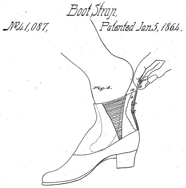
The term "bootstrap" has an interesting history. It starts with physical boots, which often had boot straps on the top, physical straps to help pull the boots on (as shown below). In the 1800s, the saying "No man can lift himself by his own boot straps" was used as a metaphor for the impossibility of improvement solely through one's own effort. (Pulling on the straps on your boots superficially seems like it should lift you off the ground, but is of course physically impossible.)

Example of a boot strap at the heel of a boot, from patent 41087, not the first boot strap patent.

Example of a boot strap at the heel of a boot, from patent 41087, not the first boot strap patent.

By the mid-1940s, "bootstrap" was used in electronics to describe a circuit that started itself up through positive feedback, metaphorically pulling itself up by its boot straps. (See usages from 1943, 1944, and 1946). By 1952, analog computers used circuits called "bootstrap integrators".

When a digital computer loaded its program through its own efforts, this took on the name "bootstrap", dating back to the 1950s. (Using a program to load a program seems as paradoxical as lifting yourself up by your bootstraps, but fortunately it works.) A 1954 glossary defined "bootstrap" as "The coded instructions at the beginning of an input tape, together with one or two instructions inserted by switches or buttons into the computer, used to put a routine into the computer." A 1955 computer survey published by the Department of Commerce had a similar definition.

Conclusion

Bootstrapping the IBM 1401 was complicated, and the process has become even more complex in later computers. In the 1960s, computers such as the IBM System/360 had bootstrap microcode stored in read-only storage. This code could load a chain of bootstrap programs, first a 64-byte bootstrap card, which would then load a 4-kilobyte bootstrap program, which could then load the disk operating system. Some early minicomputers and microcomputers lacked ROM and took a step backward, requiring the user to tediously toggle in boot code through switches on the front panel.

Modern computers go through a much more complex bootstrap process. The initial boot code for an x86 system is stored in ROM, and booting happens through the BIOS in older computers or UEFI in more modern systems. The system starts in a primitive state without caches or virtual memory, running a single core in "8086 real mode". The boot code sets up the system and loads a bootloader program, which may then load another bootloader, which loads the kernel, which starts up the computer's various processes. Details are in this presentation.

Studying the 1401's machine code shows many of its unusual characteristics compared to modern computers and the strangeness of its instruction set. Needing to deal with word marks is the most obvious difference, with special instructions to set and erase them. From a modern perspective, it's unusual to see a computer that doesn't use bytes, although that was common back then. The use of decimal arithmetic and decimal addressing also seems strange from the modern perspective. Another curiosity is self-modifying code. Although self-modifying code is discouraged nowadays, it was common on the 1401 (as with other computers of that era).

I announce my latest blog posts on Twitter, so follow me @kenshirriff. I also have an RSS feed.

Notes and references

  1. While punch cards almost always held character data, an optional feature called "column binary" allowed binary data to be punched onto cards, 12 bits in each column. IBM charged $101 a month (in 1960s dollars) for the column binary feature. 

  2. The need to fit all the data into 80 columns was one of the factors that led to the Y2K problem. If you used four columns on a card to hold the year instead of two, you'd need to give up two precious columns somewhere else. 

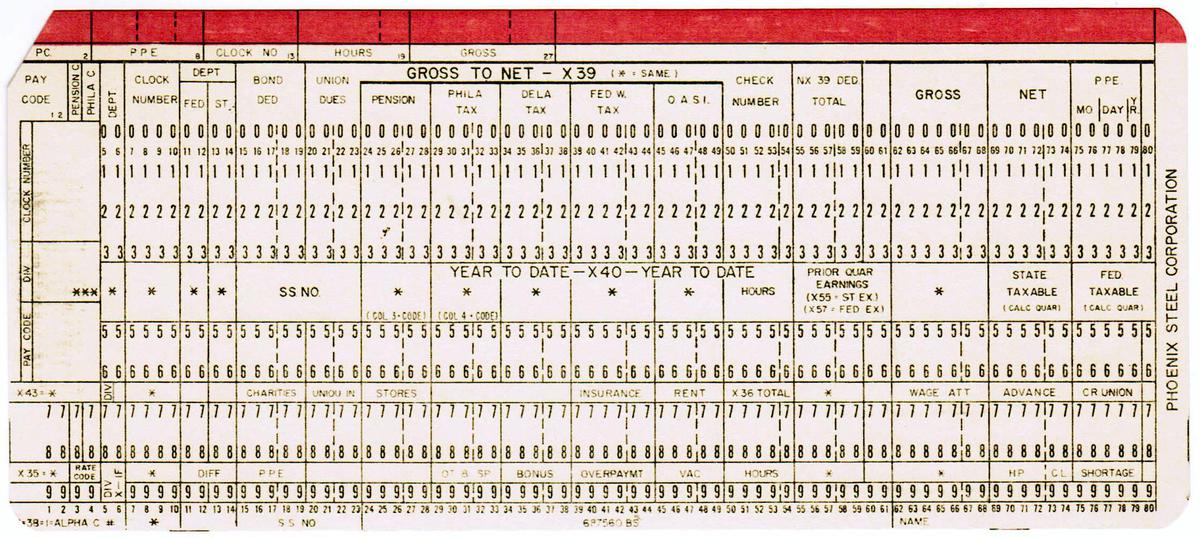
  3. The punch card below is an example of a card custom-printed for a customer application. This card was used for payroll at the Phoenix Steel Corporation.

    A punch card designed for a steel mill.

    A punch card designed for a steel mill.


  4. The operation of the load key is specified in the 1401 reference manual (p118): "This key is used to start loading instruction cards. Pressing the load key operates the read feed until a card has passed the read station. The I -address register is set to 001, and a word mark is set in address 001. All other word marks in addresses 002 through 080 are removed." The instruction in the first columns is executed, and then continued operation is controlled by the first instruction. 

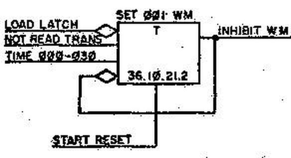
  5. How does the first word mark get set when you load the first card? I looked at the documentation of the circuitry and found the relevant flip-flop (below). It is set by the load button, sets the first word mark (WM), and then is cleared.

    The flip-flop to set word marks. From the 1401 logic diagrams, figure 81.

    The flip-flop to set word marks. From the 1401 logic diagrams, figure 81.

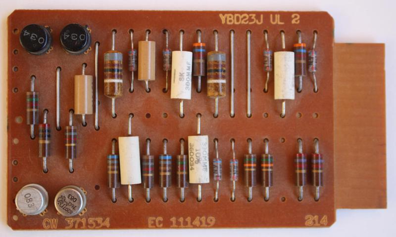
    The photo below shows the card that implements this flip-flop. With the 1401, you can actually see the physical transistors that implement each function.

    A flip-flop card, type "CW".

    A flip-flop card, type "CW".


  6. Instructions need to be indicated with word marks with a few specific exceptions. As documented in the 1401 reference manual (p15) "The 4-character unconditional branch instruction, the 7-character set word mark, and clear storage and branch instructions are the only instructions that can be followed by a blank without a word mark. All other instructions must be followed by a word mark." 

  7. The 1401 computer that I used has 16,000 characters of memory (not 16,384 because it's a decimal machine!) so after the Clear Storage instruction, the B register will hold 15,999, pointing to the top of memory. You might wonder how the address 15,999 is represented in three decimal characters. The trick is that a special address code uses the top two bits of the characters to hold the kilobyte part of the address. The resulting address is 999 with the top two bits of the hundreds and units characters set. The result is the three-character alphanumeric address I9I represents the address 15,999. 

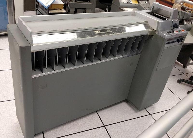
  8. If you had the misfortune to drop your cards, a card sorter could put them back in order using the sequence numbers. A card sorter rapidly sorted cards into slots based on the digit punched in one column. By running the cards through several times, you could sort on the complete sequence number. I discuss card sorters in great detail here. (A low-tech way to keep cards in order was to draw a diagonal line across the top of the cards; it helped when putting cards back in order manually.)

    An IBM Type 83 card sorter. Cards enter the machine on the right, whiz along the top of the machine, and fall into the appropriate hopper underneath.

    An IBM Type 83 card sorter. Cards enter the machine on the right, whiz along the top of the machine, and fall into the appropriate hopper underneath.

    The use of sequence numbers in columns 73-80 goes back to the Fortran language. Fortran was developed for the IBM 704 vacuum tube computer. The 704 was a 36-bit machine. The punch-card reading process used two 36-bit words, so only 72 columns could be read. (These could be any 72 columns of the card, selected by a wiring panel, but typically columns 1-72 were used.) The result was that columns 1-72 were used for code (a restriction still often used), while columns 73-80 were free for sequence numbers.