Inside the stacked RAM modules used in the Apple III

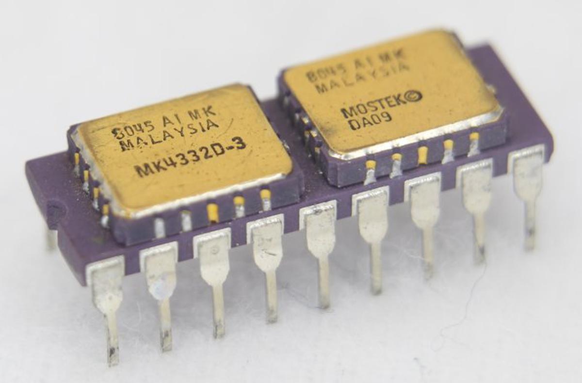
In 1978, a memory chip stored just 16 kilobits of data. To make a 32-kilobit memory chip, Mostek came up with the idea of putting two 16K chips onto a carrier the size of a standard integrated circuit, creating the first memory module, the MK4332 "RAM-pak". This module allowed computer manufacturers to double the density of their memory systems and by 1982, Mostek had sold over 3 million modules. The Apple III is the best-known system that used these memory modules.

The MK4332 memory module combined two 16-kilobit memory chips on a ceramic substrate.

The MK4332 memory module combined two 16-kilobit memory chips on a ceramic substrate.

This module was built from two 16-kilobit memory chips, constructed from the standard MK4116 dynamic RAM (DRAM) chip packaged in a leadless ceramic chip carrier; these are the golden rectangles on top of the carrier.

You might wonder why customers didn't simply use these surface-mount packages directly, but at the time soldering surface-mount components was still a challenge for many customers. However, mounting two leadless chips on a dual inline-package (DIP) carrier allowed customers to double their memory density while still using their standard through-hole soldering techniques.

The purple carrier holding the chips was a ceramic substrate designed for thermal compatibility with the chips.1 There is no circuitry inside the ceramic carrier except wiring between the chips and the eighteen DIP pins. The two memory chips were wired in parallel except for their two select lines, which were kept separate. This allowed the desired memory chip to be selected. As a result, the MK4332 module has 18 pins, compared to 16 pins for the chips on top. Mostek used the same module design with the next generation of RAM chips, creating a 128-kilobit RAM module (MK4528) from two 64-kilobit RAM chips (MK4564).

Inside the 4116 memory chip

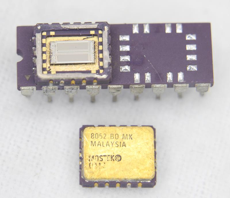
Although you might expect a complex mounting technique, the two 4116 chips are simply soldered onto the substrate with standard reflow techniques. For the photo below, I removed the metal lid from the left chip with a chisel and unsoldered the right chip with a hot air gun. On the left, you can see the rectangular silicon die inside the leadless carrier package. On the right are the 16 solder pads on the ceramic substrate. The wiring between the solder pads and the DIP pins is inside the ceramic substrate.

The MK4332 with the left package opened and the right package unsoldered.

The MK4332 with the left package opened and the right package unsoldered.

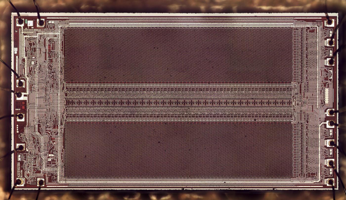
I created the die photo below from multiple microscope images. The white lines are the metal wiring on top of the chip, while the silicon underneath appears dark red. The two large rectangular regions are the 16,384 memory cells, arranged as a 128×128 matrix, split in two. The circuitry in between these regions consists of 128 sense amplifiers to amplify the bits read from memory, and selection circuitry to select one bit out of the 128. (Externally, the chip is accessed as 16,384×1, outputting a single bit. Typically, eight of these chips were used to store bytes.) The control and interface circuitry is at the left and right, connected to the external pads via tiny bond wires.

Die photo of the 4116 memory chip. Click for a larger image.

Die photo of the 4116 memory chip. Click for a larger image.

In dynamic RAM, a bit is stored in a capacitor, with a transistor providing access to the capacitor. The value of the bit is represented by the presence or absence of charge on the capacitor. The advantage of dynamic RAM is that each memory cell is very small, constructed from just two components,2 allowing a high memory density. (In comparison, static RAM may require six transistors per cell.) The downside of dynamic RAM is that the charge on a capacitor leaks away after a few milliseconds. To avoid losing data, dynamic RAM must be constantly refreshed: bits are read from the capacitors, amplified, and then written back to the capacitors. For this particular chip, all the data must be refreshed every two milliseconds.

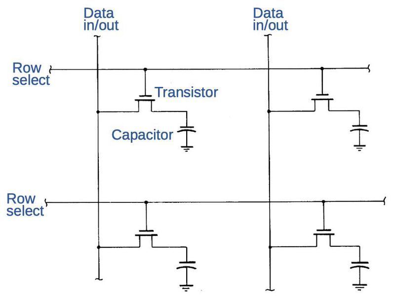
The diagram below illustrates the wiring of the memory cells, showing two of the 128 rows and columns. To read or write data, a row select line is energized. The transistors in that row turn on, connecting that row's capacitors to the data in/out lines. The data from that row is read out of the capacitors and amplified. At that point, the data can either be written back to refresh the row, or a new bit can be written. Note that although the chip accesses 128 bits in parallel internally, the chip provides access to one bit at a time externally, selecting one of the 128 bits to read or write.

Structure of the memory cells, based on the patent.

Structure of the memory cells, based on the patent.

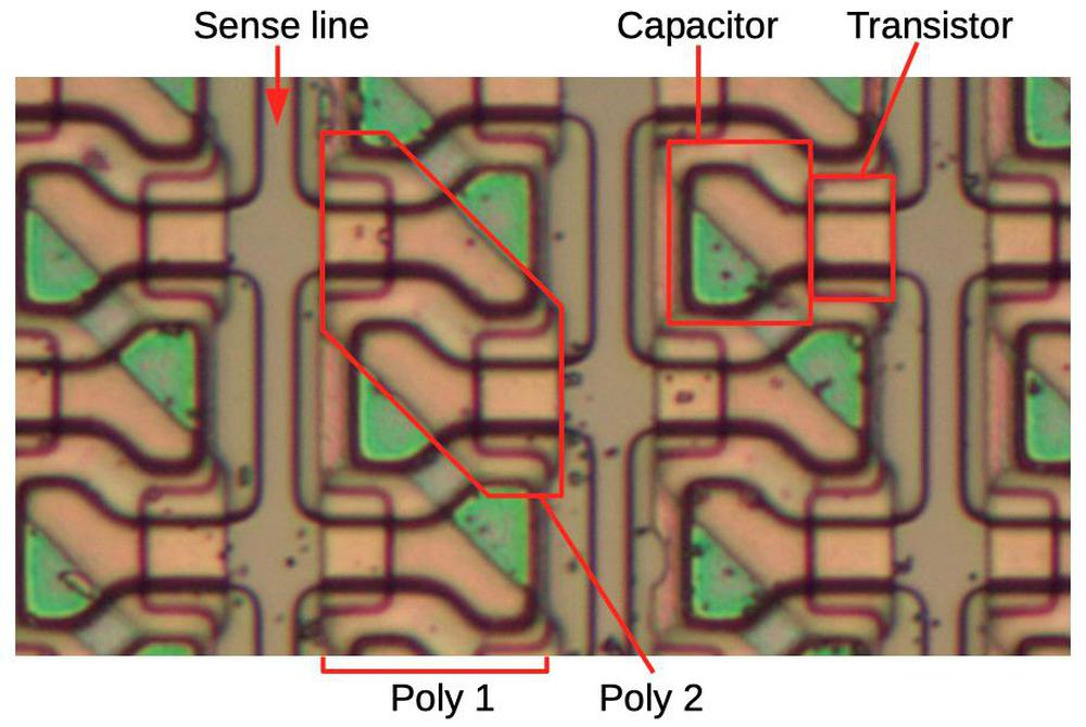
The magnified photo below shows some of the storage cells, densely packed together. It's a bit hard to visualize what's going on because the chip is constructed from multiple layers. The bottom layer is the grayish silicon die. On top of the silicon are two layers of polysilicon. Above this is the metal wiring, which was removed for this photo. The photo shows three sense lines (data in/out) in the silicon, with bulb-shaped storage cells connected on either side. Vertical strips of polysilicon (poly 1) over the storage cells implement capacitors: the silicon forms the lower plate, while the polysilicon forms the upper plate. The second layer of polysilicon (poly 2) is arranged in diagonal regions to implement the selection transistors. Square notches in the poly 1 layer allow the poly 2 layer to approach the silicon to form transistors. Horizontal metal wiring (not visible) is connected to the poly 2 regions to select a row by driving the transistors. Note that the rows are staggered and interlocking (kind of like a zipper) due to the highly-optimized layout. At the time, fitting this much memory on a chip was a challenge that pushed the limits of integrated circuit technology.

A closeup of the memory chip under the microscope, showing individual storage cells.

A closeup of the memory chip under the microscope, showing individual storage cells.

Memory chips in the Apple III

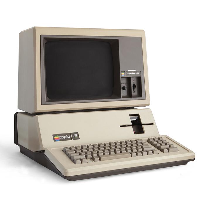
Apple was a major customer of these memory modules, using them in the Apple III computer (1980). The Apple III was marketed as a business computer to follow the popular Apple II. Unfortunately, the Apple III was a business failure due to reliability issues and competition from the IBM PC introduced a year later.

Apple III Plus computer. Photo by Bilby, CC BY 3.0.

Apple III Plus computer. Photo by Bilby, CC BY 3.0.

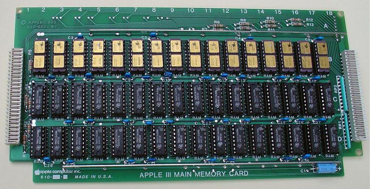
As was usual for the time, the Apple III's memory board3 was stuffed with memory chips to achieve more capacity. An unusual part of the design is it used three rows of memory chips (instead of a power of two), mixing 16-kilobit and 32-kilobit memory chips to achieve 128 kilobytes of storage. (The Apple III's case was designed before the boards, so the boards had to be designed to fit the available space.) In the photo below, the top row holds MK4332 memory modules, while the bottom two rows hold 16-kilobit MK4116 chips.4

Apple III main memory card. Photo courtesy of DigiBarn, CC BY-NC 3.0

Apple III main memory card. Photo courtesy of DigiBarn, CC BY-NC 3.0

A brief history of memory

Memory is an under-appreciated part of computing. The CPU usually gets the attention, but memory was often the limiting factor. The problem with memory is that storing a single bit is easy, but most approaches are impractical when you try to scale up to thousands or millions of bits.

The early ENIAC computer (1946) used vacuum tubes for storage, but these were bulky and expensive, limiting ENIAC to just 20 words (of 10 digits) stored in its accumulators. Early computers such as EDSAC (1949) used mercury delay lines for memory, sending pulse trains of sound waves through tubes of mercury. Although EDSAC could store 512 words, you had to wait for bits to circulate serially through the mercury. An improvement was the random-access Williams tube which stored data as spots on a cathode-ray tube screen. Although they were temperamental, Williams tubes were used in the Manchester Mark 1 (1949) and the commercial IBM 701 (1952).

The introduction of core memory revolutionized computing, providing fast, cheap, and reliable storage, storing each bit in a tiny magnetized ferrite ring. Core memory was introduced in the Whirlwind computer (1953) and used in most computers of the late 1950s and 1960s. However, since each bit required a separate physical ferrite core, memory sizes were limited to a few megabytes for even the largest customers. For example, memory cabinets for the IBM System/360 (1969) held 256 kilobytes but weighed over a ton each (below).

Magnetic core memory was relatively bulky. This photo shows an IBM System/360 Model 85 installation. The cabinets in the front are IBM 2365 Processor Storage, each holding 256 kilobytes. The double-H cabinet in the center is the CPU. Photo from IBM.

Magnetic core memory was relatively bulky. This photo shows an IBM System/360 Model 85 installation. The cabinets in the front are IBM 2365 Processor Storage, each holding 256 kilobytes. The double-H cabinet in the center is the CPU. Photo from IBM.

Semiconductor memory led to another dramatic shift. At first, semiconductor memory was costly and had very small capacity; Intel's first product was a memory chip holding just 64 bits and costing $99.50. In 1968, Dennard at IBM invented cost-effective dynamic RAM and semiconductor DRAM technology advanced quickly at various companies. Intel introduced the first commercially available DRAM chip in 1970, the i1103 holding 1K bits. This chip was nicknamed the "core killer" because of its impact on the magnetic core memory industry.

Computer storage rapidly moved from core memory to DRAM as the capacity of DRAM increased and the price fell.5 Mostek introduced the 4-kilobit MK4096 chip in 1973, followed by the 16-kilobit MK4116 in 1976. In 1978, Fujitsu introduced the first commercial 64-kilobit DRAM chip and Japan took the lead in DRAM manufacturing.6 Intel left the DRAM industry in 1985 due to decreasing market share and profits, followed by the remaining US DRAM manufacturers.

Fifty years after the introduction of DRAM, it is still the dominant technology for main storage, a remarkably long lifetime. Compared to the 16-kilobit chip I described, Samsung's recent 16-gigabit DRAMs are a factor of a million larger, showing the incredible increase in density. It remains to be seen if anything will challenge the long storage leadership of DRAM.

I announce my latest blog posts on Twitter, so follow me at kenshirriff. I also have an RSS feed. Thanks to Mike Braden for suggesting the MK4332 chip to me.

Notes and references

  1. For details on the construction of the memory modules, see Rectangular chip-carriers double memory-board density, Electronics, 1982. 

  2. Early dynamic RAMs such as the Intel 1103 used three transistors per cell and used separate lines for reading and writing data. Improvements in memory technology shrunk the circuit to a single transistor and a single data line. 

  3. The Apple III memory board pictured is the "12 volt memory board", given that name because the memory chips required 12 volts (as well as +5 and -5). It was upgraded by the "5 volt memory board", which used only a 5 volt supply. The 5 volt memory board used more modern 64-kilobit memory chips (4864) giving it a larger capacity of 128 or 256 kilobytes. Inconveniently, the power supply required a 12-volt load to operate, so the 5-volt memory board has a power resistor to draw 0.4 amps from the otherwise-unused 12-volt supply. Details are in the Apple III reference manual

  4. The Apple III memory board was also available in a lower-cost 96-kilobyte module. In that configuration, the 4332 memory modules were replaced with the 16-kilobit (MK4116) chips used on the rest of the board. One clever feature of the 4332 module is the two "extra" select pins are on the end of the package. The result is that a memory board (such as the Apple III's) can be designed to accept either the 16-pin 16-kilobyte chips or the 18-pin 32-kilobyte modules, depending on how much memory is desired. With the smaller chips, the two extra pins are unused. It's strange, however, that the Apple III memory board only accepted the larger modules in one of the three rows of chips. 

  5. The industry switch from magnetic core memory to semiconductor memory wasn't as straightforward as superior semiconductor memory overthrowing inferior core memory. Instead, there was a time period where they co-existed, due to tradeoffs. For instance, in 1972, a customer could select core memory, semiconductor memory, or a mixture for the D-112 minicomputer (a PDP-8 clone); semiconductor memory was 5 times faster, but core memory supplied four times the capacity per board. By 1973, industry publications were reporting that "Semiconductor memories are taking over data-storage applications". As late as 1980, core memory manufacturers were advertising the benefits of core memory, battling the "myths" that semiconductor was better.

    Was the overthrow of magnetic core by semiconductor memory inevitable? My view is that "technological determinism" acts in some ways; the development of DRAM memory was almost unavoidable following the development of MOS transistors. However, "economic determinism" was more responsible for the success of semiconductor memory: if magnetic core had remained the lower-cost option, it probably would have remained dominant. As a counterexample, CCD (charge-coupled device) memory and bubble memory were hyped as storage technologies of the future, but couldn't achieve the price-performance to dislodge either semiconductor memory or hard disks. 

  6. Note that the capacity of memory chips increased by a factor of 4 each generation (1-, 4-, 16-, 64-kilobit) rather than a factor of 2. The reason is that each address pin was multiplexed to provide two address bits, so each additional address pin resulted in a factor of four increase. By reusing each address pin for both a row address and a column address, the number of address pins was kept low so compact 16-pin packages could be used even as memory sizes expanded to 256-kilobit. Conveniently, as technology improved, memory chips required fewer voltages, freeing up pins formerly used for power. One consequence, though, was the ordering of address pins on the chip was essentially random as new address pins were assigned based on which pins were available, rather than sequentially. The multiplexed address system was introduced in the Mostek MK4096 chip and meant that the 256-kilobit 41256 chip used fewer pins than the original 1-kilobit Intel 1103 (16 pins vs 18). 

How the bootstrap load made the historic Intel 8008 processor possible

Near the end of 1972, Intel introduced their first 8-bit microprocessor, the 8008. Decades later, this processor still influences computing; you probably use an x86 processor that is a descendent of the 8008. One unusual feature of the 8008 processor is its use of a "bootstrap load" or "bootstrap capacitor", a special capacitor circuit to improve performance.1 Federico Faggin, who led the development of the 8008, is the main character in this story; he invented a new way to fabricate bootstrap capacitors for the Intel 4004 and 8008 processors and says it "proved essential to the microprocessor realization" and "without [the bootstrap load], there was no microprocessor."

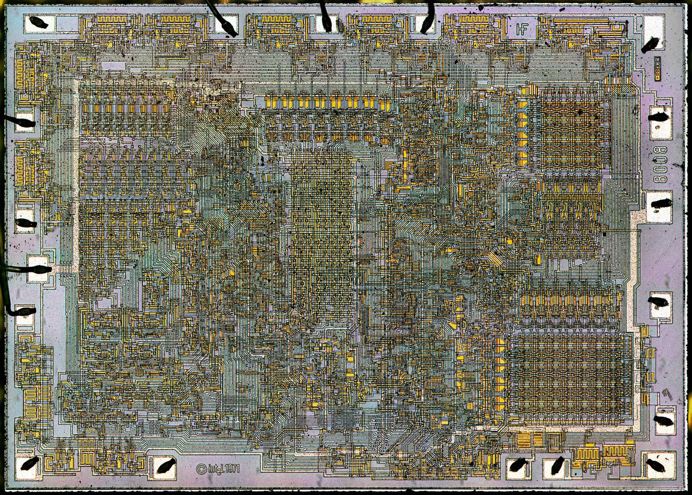
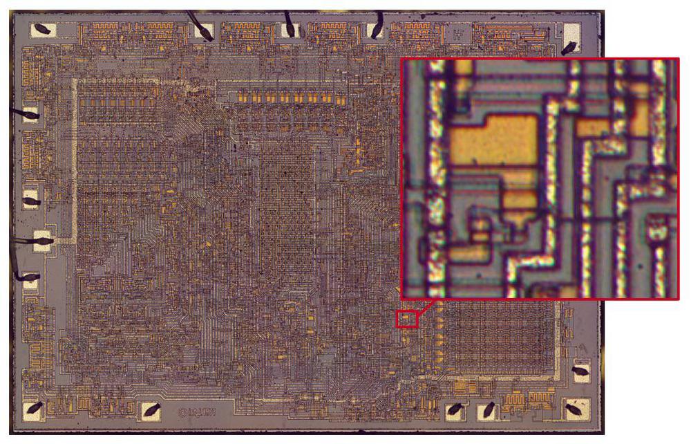
Die photo of the 8008 microprocessor. (Click for a larger image.)
The initials HF appear on the top right for Hal Feeney, who did the chip's logic design and physical layout.

Die photo of the 8008 microprocessor. (Click for a larger image.) The initials HF appear on the top right for Hal Feeney, who did the chip's logic design and physical layout.

My photo above shows the tiny silicon die inside the 8008 package. You can barely see the wires and transistors that make up the chip. There are 90 bootstrap capacitors, visible as small yellow rectangles, especially in the upper center. The squares around the outside are the 18 pads that are connected to the external pins by tiny bond wires. 18 pins is a very small number for a microprocessor, but Intel was bizarrely committed to small packages at the time.2 This required inconvenient tradeoffs; the lack of multiple power pins was one factor forcing the use of bootstrap loads.

The 8008 processor's history is more complex than you might expect. Its roots are the Datapoint 2200, a popular computer introduced in 1970 as a programmable terminal. Created before the microprocessor, the Datapoint 2200 contained a board-sized CPU build from individual TTL chips. Datapoint talked with both Intel and Texas Instruments about replacing the processor board with a single MOS chip. Texas Instruments created the TMX 1795 processor in March 1971, while Intel created the 8008 around the end of 1971 but Datapoint rejected both chips for a variety of reasons. Texas Instruments abandoned the TMX 1795 after their attempts to market it failed. Intel, on the other hand, marketed the 8008 as a general-purpose microprocessor, creating the microprocessor industry.

(You might wonder how the Intel 4004 fits into this story. The Intel 4004 is architecturally unrelated to the 8008 in almost every way; despite the similar names, the 8008 is not an 8-bit version of the 4-bit 4004. After the Intel 4004 was launched in 1971, much of the 4004 team (including Faggin, Hoff, Mazor, and Feeney) moved over to the 8008 project. Because the 4004 and 8008 processors were built by the same team with the same PMOS3 process, they have some layout and circuit-level similarities, in particular the bootstrap load circuit.)

Why the bootstrap load?

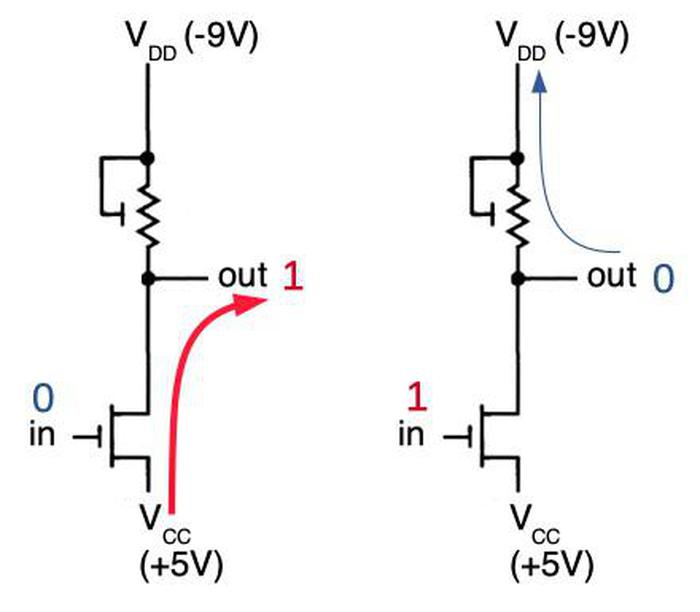
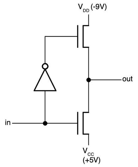
The purpose of the bootstrap load is to get extra voltage out of a transistor when necessary. To explain this, I'll start by showing how an inverter works when implemented in a processor. The diagram below shows an inverter, built from a PMOS3 transistor and a load resistor (which is actually a transistor). If the input to the inverter is 0 (low), the lower transistor turns on, pulling the output high (1). But if the input is 1 (high), the output transistor turns off. In that case, the load resistor pulls the output low (0). Thus, the input signal is inverted.

How an inverter is constructed from PMOS transistors. The upper symbol indicates a PMOS transistor that is acting as a load resistor.  Based on the 8008 datasheet.)

How an inverter is constructed from PMOS transistors. The upper symbol indicates a PMOS transistor that is acting as a load resistor. Based on the 8008 datasheet.)

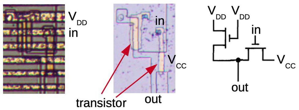
The diagram below shows the physical implementation of an inverter in the 8008 processor. The first die photo shows the inverter as it appears in the chip. The horizontal metal wiring on top provides VDD and the input to the circuit. For the second photo, I dissolved the metal layer to reveal the two transistors that form the circuit. The schematic on the right matches the physical layout of the transistors on the die but otherwise corresponds to the schematic above. Because creating resistors in an integrated circuit is inconvenient, the load resistor is implemented by a transistor.

How an inverter appears in the 8008 processor.

How an inverter appears in the 8008 processor.

There's a complication from using a transistor as a load resistor: these MOS transistors have a property called the threshold voltage VT. The problem is that when you try to pull a signal low, the transistor can't pull it all the way low. Although you'd like the signal to get pulled down to VDD (-9 volts), the threshold voltage (say -5 volts)9 means that you can only get the signal down to -4 volts. (This is one of the reasons why the 8008 requires a much larger voltage (15 volts overall) than modern integrated circuits; if you tried to run it at 5 volts, the threshold voltage would consume the entire signal.)

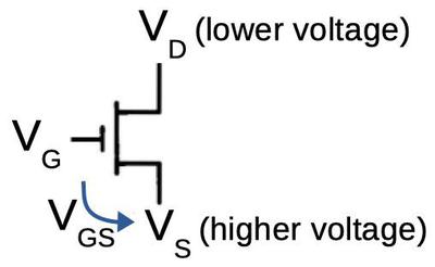
The diagram below explains the threshold voltage in more detail. VD, VG, and VS are the voltages on the drain, gate, and source respectively. VGS is the voltage between the gate and the source. The transistor will turn on if VGS < VT, the threshold voltage. (Inconveniently, most of these voltages are negative in a PMOS transistor, which makes things confusing.) The problem is that with a gate voltage of -9 volts and a threshold voltage of -5 volts, the transistor will only be on if VS is higher than -4 volts. Thus, the transistor can't pull VS lower than -4 volts. The only way to get VS lower is if you had a more-negative gate voltage, at least -14 volts in this case. Some chips solve this by using an additional voltage supply to provide more voltage to the gate, such as the Intel 8080 or the HP Nanoprocessor.

VD, VG, and VS are the voltages on the transistor's drain, gate, and source respectively. VGS is the voltage difference between the gate and source.

VD, VG, and VS are the voltages on the transistor's drain, gate, and source respectively. VGS is the voltage difference between the gate and source.

The threshold voltage isn't much of a problem when you're dealing with inverters and other gates, because the voltage levels are restored by each gate. However, there are two places where the threshold voltage is a problem: superbuffers and pass transistor logic. In these circuits (described in the footnote4), the threshold voltage drop happens twice, yielding an output that is too weak. Since these circuits are common in processors, a solution was needed: the bootstrap load. It is a way of generating more voltage for the gate to overcome the threshold voltage so the transistor to pull its output all the way to VD.

How the bootstrap load works

The bootstrap load is essentially a charge pump circuit that uses a bootstrap capacitor to boost the gate voltage. The diagram below shows the basic idea of a charge pump. On the left, a capacitor is charged to -9 volts from a voltage source. If you disconnect the voltage source and then re-connect the negative side to the capacitor as shown on the right, the capacitor retains its charge of -9 volts. However, since the lower side of the capacitor is now at -9 volts, the upper side of the capacitor is now at -18 volts. The bootstrap load uses this -18 volts as the gate voltage, sufficient to overcome the threshold voltage.

A charge pump. On the left, the capacitor is charged to -9 volts. On the right, the bottom of the capacitor is connected to -9 volts, yielding -18 volts on top of the capacitor.

A charge pump. On the left, the capacitor is charged to -9 volts. On the right, the bottom of the capacitor is connected to -9 volts, yielding -18 volts on top of the capacitor.

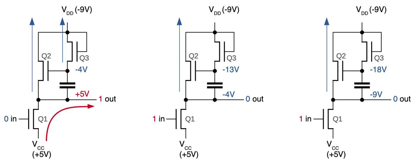
The diagram below shows the bootstrap load circuit. The circuit is similar to the inverter described earlier, but with the addition of a capacitor and a transistor. In the first diagram, a 0 input turns on the lower transistor (Q1), yielding a 1 output (+5 volts). Meanwhile, Q3 acts as a load resistor, pulling the top of the capacitor to -4 volts (not -9 volts due to the threshold voltage.) This results in -9 volts stored across the capacitor.

How the bootstrap load circuit works.

How the bootstrap load circuit works.

The second and third diagrams show what happens with a 1 input. The lower transistor Q1 turns off, allowing Q2 to pull the output low. With a regular inverter, -4 volts is as low as the output can go (second diagram). However, as explained earlier, the capacitor still holds -9 volts, so the top of the capacitor must be -13 volts. With -13 volts on the gate of Q2, Q2 will continue to pull the output lower, until the circuit ends up as shown on the right, with the output pulled all the way down to -9 volts. Note that the source can't get pulled down any lower than the drain, regardless of the gate voltage. (In comparison, the simple inverter described earlier could only pull the output down to -5 volts.)5

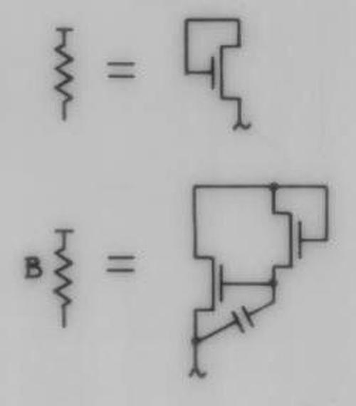
The image below shows part of Intel's schematic for the 4004 processor, showing the circuit for a standard load and the circuit for the bootstrap load, indicated by a "B" next to the resistor.

Representation of the bootstrap load on the Intel 4004 schematic. The resistor with "B" symbolizes the bootstrap load circuit next to it.

Representation of the bootstrap load on the Intel 4004 schematic. The resistor with "B" symbolizes the bootstrap load circuit next to it.

The silicon-gate bootstrap load

So far, I've discussed the bootstrap load, which was extensively used with MOS circuitry, and was patented by North American Rockwell in 1966. The invention necessary for the 4004 and 8008 processors was the extension of the bootstrap load to silicon-gate integrated circuits.

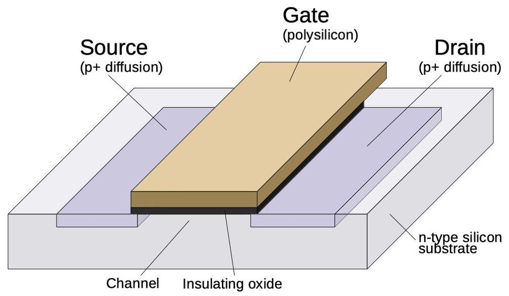
One of the key inventions that made the 8008 practical was the self-aligning silicon gate transistor.6 The diagram below shows the structure of an MOS transistor. Early MOS integrated circuits used metal-gate 7 transistors, which used metal, typically aluminum, instead of polysilicon for the gate. But at Fairchild in 1968, Faggin and Klein invented a practical way to make transistors with silicon gates. This may seem like a trivial difference, but silicon-gate transistors were better than metal-gate transistors in three important ways. First, the electrical properties of silicon-gate transistors are much better than metal-gate transistors, running faster and at lower power. Second, polysilicon provided a second layer for routing signals, making integrated circuit layouts much more compact.

Structure of a PMOS transistor.

Structure of a PMOS transistor.

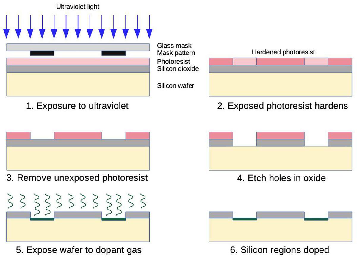
Finally, polysilicon permitted construction of self-aligned transistors, which play an important part in the bypass capacitor story. Integrated circuits are constructed through a sequence of processing steps, using optical masks and photo-sensitive resist to create patterns on the surface. An integrated circuit with metal-gate transistors is constructed from the bottom up. First, the source and drain regions are doped with impurities to form P-type silicon, as shown below. In a later step, the metal gate is created between the source and the drain, using a different mask. The tricky part is making sure the gate is lined up with the source and the drain; if there's a gap, the transistor won't work. Thus, a metal gate is made larger than necessary so it will still cover the gate channel, even if the alignment of the layers is slightly off. Unfortunately, this overlap creates capacitance and harms performance.

How a photomask is used to dope regions of silicon.

How a photomask is used to dope regions of silicon.

On the other hand, the self-aligned gate is created in the opposite order. The polysilicon gate is created first. In a later step, the source and drain regions are doped. However, a mask isn't used to separate the source and drain from the gate. Instead, the gate itself blocks doping of the region in between the source and drain. Thus, the source and drain are automatically "self-aligned" with the gate, eliminating the excess capacitance from a too-large gate. (Why couldn't metal gates be self-aligned? Because doping the silicon requires high temperatures that would melt the metal, but polysilicon can handle the heat.)

Although self-aligned silicon gates are a major improvement over metal gates, there was one drawback: capacitors. With metal-gate transistors, a capacitor could be easily constructed by using metal and doped silicon as the plates: a large metal layer on top, doped silicon underneath, and a thin insulating oxide layer in between. (In other words, a transistor with a large gate is used as a capacitor.) With self-aligned gates, the polysilicon gate could be used as a capacitor plate in place of the metal layer. However, in the self-aligned process, the polysilicon gate blocks doping of the silicon underneath, which is good for a transistor but bad for a capacitor, since you can't dope the silicon under the polysilicon plate. (You could use an extra manufacturing step to dope the capacitor plates before creating the polysilicon gate, but this extra step would increase the cost.)

Faggin invented a solution that made capacitors practical with self-aligned gates.8 He realized that if you bias the capacitor correctly, the charge on the upper plate will create a conductive region in the silicon underneath it, even without any doping. He tried this at Fairchild and discovered that it worked. This solved the problem of how to use a bootstrap load with self-aligned silicon-gate transistors.

Closeup of a bootstrap load circuit in the 8008.

Closeup of a bootstrap load circuit in the 8008.

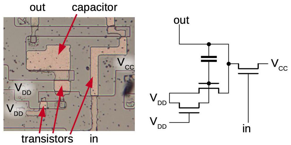
The photo above zooms in on one of the boostrap load circuits in the 8008, used in an inverter. The diagram below shows the underlying silicon after removing the metal layer. The bootstrap capacitor is constructed by a layer of polysilicon (pinkish) over the underlying silicon, forming the capacitor plates. The transistor on the right inverts the input. The capacitor is charged by the transistor in the lower left. The load transistor is in the middle; the capacitor provides the boosted voltage to its gate. The transistors have varying sizes depending on their roles. The inverting transistor is the largest since it provides the most current. The transistor that charges the capacitor is very small in comparison because a small current can keep the capacitor charged.

The circuitry of an inverter with a bootstrap load.

The circuitry of an inverter with a bootstrap load.

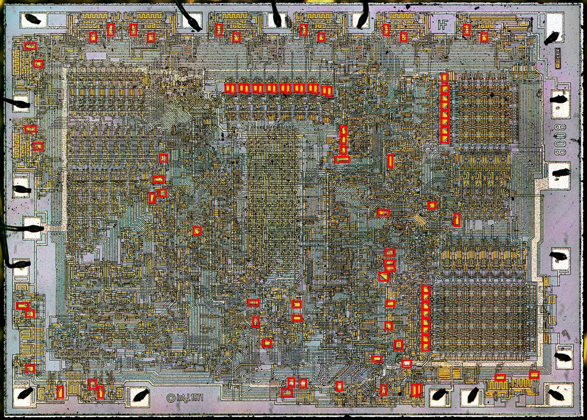
This bootstrap load technique was extensively used in the 4004 and 8008 processors. The diagram below shows the bootstrap loads in the 8008 processor, indicated with a red box. The 8008 has 90 bootstrap loads, so it is a significant circuit. Many bootstrap loads are around the periphery of the chip to help drive the output pins. The instruction register (upper center) uses bootstrap loads to drive the relatively large instruction decoder (center). At the right, bootstrap loads drive the register storage (upper right) and stack storage (lower right). Other miscellaneous circuits throughout the processor also use bootstrap loads.

The bootstrap loads in the 8008 are indicated by red boxes.

The bootstrap loads in the 8008 are indicated by red boxes.

Conclusion

A final question is if the bootstrap load was a key invention that made the microprocessor possible (as embodied in the 4004 and 8008) or if the microprocessor was inevitable regardless of features such as the bootstrap load. One view is that "the buried contact and particularly the bootstrap load, were indispensable to obtain the required speed within the available power budget." Feeney said in an 8008 oral history "that being limited on pins, limited on power supplies, whatever, that the bootstrap load became very, very critical." On the other hand, the development of the microprocessor seemed an inevitable, incremental process to many. Fairchild engineer Lee Boysel said in 1970,10 "The computer-on-a-chip is no big deal. It's almost here now... I've no doubt the whole computer will be on one chip within five years." Hal Feeney of Intel said, "a the time in the early 1970s, late 1960s, the industry was ripe for the invention of the microprocessor."

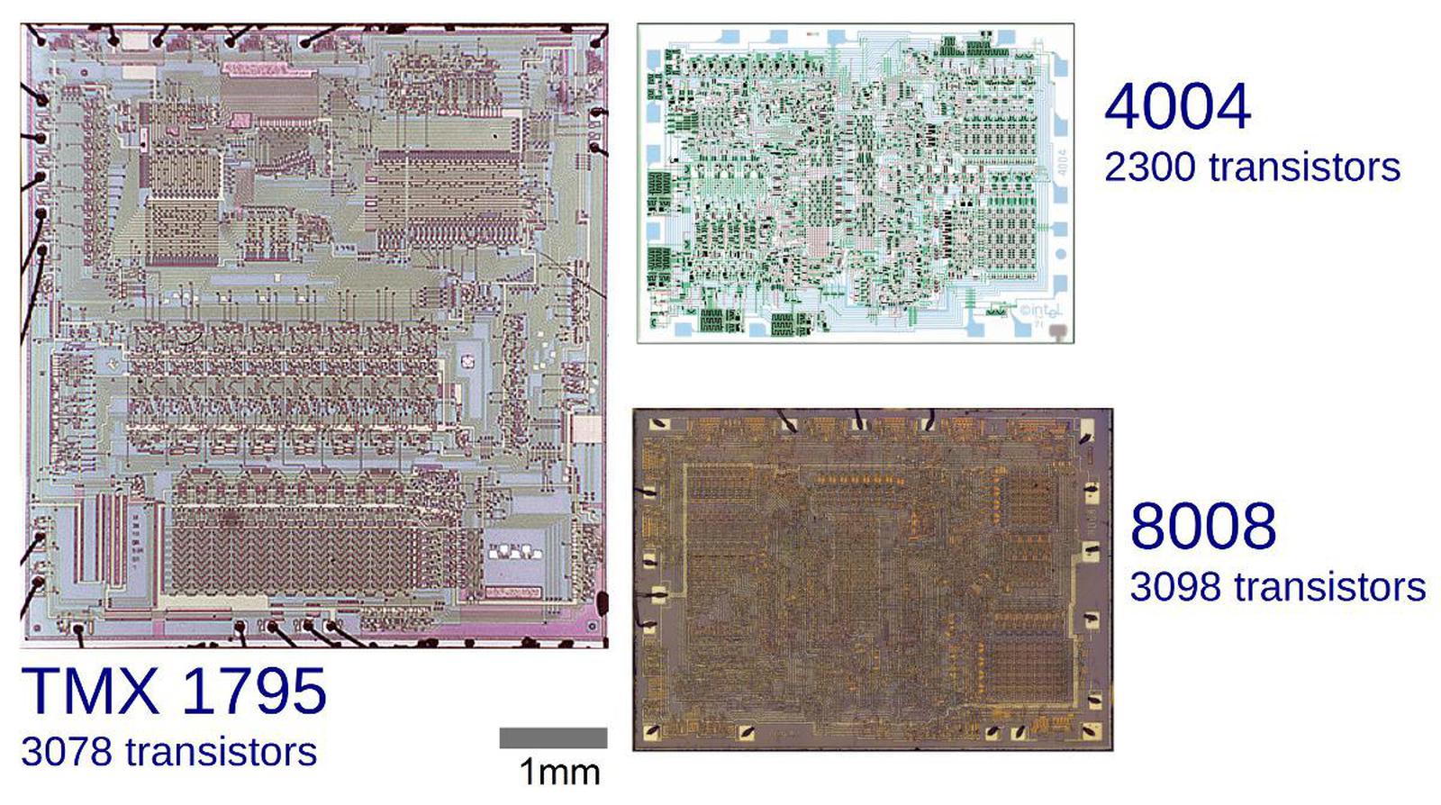
In the narrow sense, the bootstrap load made the 4004 and 8008 possible with their given size, performance, and power consumption. The bootstrap load also illustrates how the microprocessor is not a single invention, but the aggregation of many smaller inventions that made it possible. However, looking at the broader picture, microprocessors would have been only slightly hampered if the bootstrap capacitor didn't exist. There were many alternatives such as four-phase logic, static logic, higher gate voltages, an additional power supply, or using an extra mask for the capacitors. The Texas Instruments TMX 1795 provides a direct comparison, since it was built at the same time as the 8008 with the same architecture, but using metal-gate transistors instead of silicon-gate. The diagram below shows that the TMX 1795 was considerably larger than the 8008, and it had somewhat worse performance, but the point is that microprocessors would have proceeded essentially the same without the bootstrap load. In any case, by 1974, the switch to NMOS transistors and improvements in threshold voltages made bootstrap loads unnecessary. My conclusion is that the bootstrap load was a helpful innovation, but microprocessors would have proceeded along a similar path even without this invention. Once technology permitted a few thousand transistors to be constructed on an integrated circuit, the single-chip CPU was inevitable.

Comparative die sizes of the TMX 1795, 4004 and 8008 microprocessors. Note that the 4004 and 8008 are nearly the same size, while the TMX 1795 is more than twice as large. The top third of the TMX 1795 is instruction decoding and control logic, the middle is the 8-bit ALU, and the bottom is storage (stack and registers). TMX 1795 die photo courtesy of Computer History Museum.

Comparative die sizes of the TMX 1795, 4004 and 8008 microprocessors. Note that the 4004 and 8008 are nearly the same size, while the TMX 1795 is more than twice as large. The top third of the TMX 1795 is instruction decoding and control logic, the middle is the 8-bit ALU, and the bottom is storage (stack and registers). TMX 1795 die photo courtesy of Computer History Museum.

If you're interested in the 8008, my previous article has a detailed discussion of the 8008's architecture and more die photos; I also explain the 8008's ALU. I announce my latest blog posts on Twitter, so follow me at kenshirriff. I also have an RSS feed.

Notes and references

  1. Bootstrap loads in the Intel 4004 are discussed by Insanity 4004 here and here

  2. In his oral history, Faggin describes Intel's fixation on 16-pin packages. When a memory chip required 18 pins instead of 16, it was "like the sky had dropped from heaven. I never seen so [many] long faces at Intel, over this issue, because it was a religion in Intel; everything had to be 16 pins, in those days. Everything had to be 16 pins... It was a completely silly requirements to have 16 pins." At the time, other manufacturers were using 40- and 48-pin packages, so there was no technical limitation, just a minor cost saving from the smaller package. 

  3. The classic microprocessors such as the 8080, 6502, and Z-80 were built with NMOS transistors. The earlier 4004 and 8008 used PMOS transistors, which were easier to manufacture but had poorer performance. If you're familiar with NMOS logic, PMOS logic is a mirror world, where everything is backward. PMOS used negative voltages, which were also significantly higher than the 5 volts used by standard TTL. For compatibility with TTL levels, the 8008 ran with Vcc at +5V and Vdd at -9V, so it could produce TTL-compatible outputs of roughly 0 volts and 5 volts. (See the datasheet for more details.) The 4004 required -15 volts, typically Vdd = -10V and Vss = +5V. Confusingly, the 4004 defined logic "0" as the more positive voltage and logic "1" as the more negative voltage (datasheet). 

  4. The "superbuffer" replaces the load resistor with an active transistor and is used when more current is required, for instance to drive an internal bus or an output pin. The upper transistor is driven by an inverter, so it is on when the lower transistor is off. Instead of the weak current from the load resistor/transistor, this transistor provides a high current. The problem is that the threshold voltage limits the voltage from the upper transistor. With a regular inverter, the inverter output loses VT, so it will provide -4 volts to the upper transistor's gate. Losing another VT there yields an insufficient output voltage of +1 volt instead of the desired -9 volts.

    A superbuffer provides a fast, high-current output in both directions.

    A superbuffer provides a fast, high-current output in both directions.

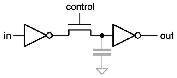
    The second case where the threshold voltage drop is a problem is with a pass transistor, used for dynamic logic. The diagram below illustrates a simple pass transistor circuit. When the control signal is low, the transistor is active, passing the input signal through to the output. But when the control signal is high, the transistor stops passing the input. Instead, the previous value is held by the circuit's capacitance (shown in gray) so the output holds its previous value. Thus, pass transistors provide an efficient way of implementing temporary storage. The problem with pass transistors is the threshold voltage. If the control signal on the gate comes from a regular gate, the "on" voltage will be -4 volts due to the threshold voltage loss. The pass transistor causes a second threshold voltage loss, so the lowest it can pull its output is +1 volt, not enough for reliable operation.

    A simple pass-transistor circuit.

    A simple pass-transistor circuit.

    The bootstrap load fixes these problems. By putting a bootstrap load on the inverter in the superbuffer or on the circuit controlling the pass transistor, the drive voltage will be close to -9 volts. Now there is only a single threshold voltage drop, leaving the output at -5 volts, sufficiently negative for reliable operation. 

  5. This discussion of the bootstrap load is a simplified explanation. The real circuit is affected by stray capacitance, transistor leakage, and other factors, so the output wouldn't be all the way to VDD. One thing I'd like to point out, though, is that you might expect the capacitor's charge to leak out through Q3 as fast as it charged. Although Q3 is treated as a resistor, it also acts as a diode, blocking the capacitor from discharging. (With the capacitor more negative, the roles of Q3's source and drain are reversed and it no longer conducts.) 

  6. The silicon-gate bootstrap capacitor exemplifies the paths of information between companies at the dawn of the microprocessor era. Practical silicon gate technology was created at Fairchild (with some earlier roots). When employees (including Faggin) left Fairchild for Intel, they took this knowledge with them. (And in some cases took "lots and lots of Fairchild internal confidential documents", see Shima oral history). From Intel, ideas spread to other companies, such as when Faggin leaving Intel to found Zilog, basing the Zilog Z80 on the Intel 8080.  

  7. Interestingly, in 2007 Intel started using metal gates again in order to scale transistors further (details). In a way, semiconductor technology has gone full circle, back to metal gates, although now unusual metals such as hafnium are used. 

  8. In the making of the first microprocessor, Federico Faggin says, "bootstrap load was a very popular circuit design trick used in just about all MOS dynamic circuits of that time. It made possible an output signal swing that was not only equal to the power supply voltage, but was also faster than possible with normal MOS loads for the same power dissipation." Faggin describes how he invented the bootstrap load in the 4004 oral history (p11) and the 8008 oral history (p8). Also see Faggin's The MOS silicon gate technology and the first microprocessors. He describes how the bootstrap load is needed for a two-phase design, and how silicon gate technology didn't support capacitors. Faggin's site describes the bootstrap load. Bootstrap load is also described at mosgate

  9. The threshold voltage depends on various properties of the integrated circuit including the gate material and the oxide thickness. I couldn't find a specific value for the threshold voltage in the 8008 processor, but -5 volts seems like the right ballpark (and is a conveniently round number). The book MOSFET in Circuit Design discusses threshold voltages for P-channel devices.  

  10. The bootstrap load illustrates the social process through which people are assigned credit for inventions and the construction of reputation. Although Faggin had a key role in the 4004 and 8008 processors, "when he left to found Zilog he got temporarily written outside of the Intel history." (See Intel disowns Faggin and Interview with San Mazor.) Faggin states, "They tried to erase my name from all of my contributions, including the silicon gate technology and the first microprocessor, and attribute them to others." After lobbying efforts by Faggin's wife and the pro-Faggin website intel4004.com, Intel reluctantly gave Faggin more credit. Faggin eventually received various awards including the National Medal of Technology and Innovation in 2010, so in the end he received his (deserved) recognition.

    The point is that credit is not assigned objectively, but is a dynamic force depending on various corporate and personal forces and who tells the story. (Wikipedia is one modern arena for these conflicts.) One corrective is the book History of semiconductor engineering, which covers many of the key people in the history of integrated circuits, with little regard for the "generally accepted" history. I should make it clear that I am drawing most heavily on Faggin's writings for background on the bootstrap load, so this blog post should not be viewed as an "objective" view of who should get credit for it. It looks like the silicon-gate bootstrap load was invented simultaneously at National Semiconductor; patent 3912948 filed in 1971 by Dilip Bapat describes an identical silicon-gate bootstrap load circuit. 

How to multiply currents: Inside a counterfeit analog multiplier

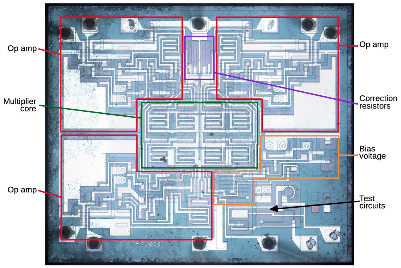
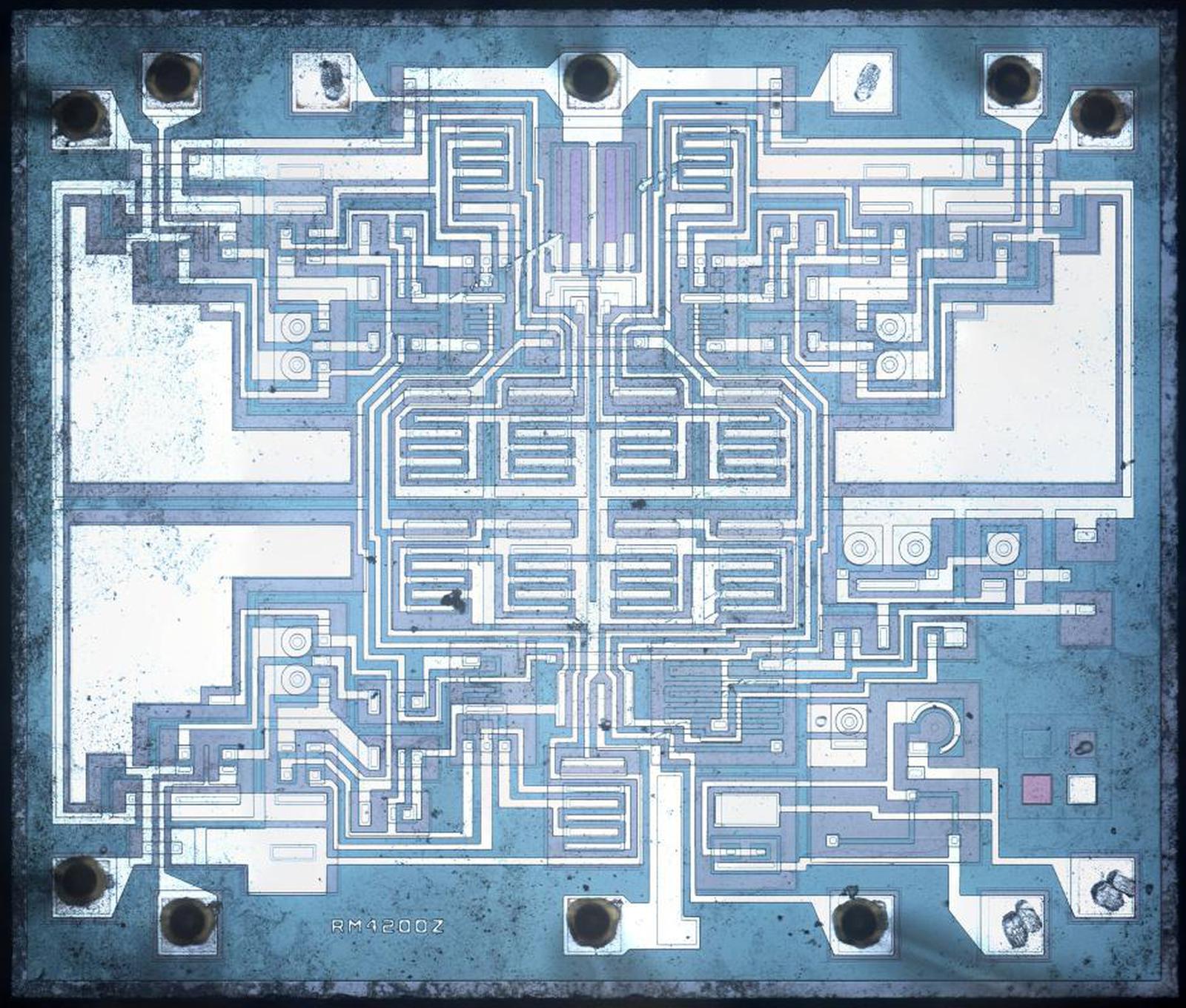
A recent Twitter thread about a counterfeit analog multiplier chip attracted my attention since I'm interested in both counterfeit integrated circuits and how analog computers multiply. In the thread, John McMaster decapped a suspicious AD633 analog multiplier chip and found an entirely different Rockwell RC4200 die inside. Why would someone do this? Probably because the RC4200 (1978) currently sells for about 85 cents, while the more modern laser-trimmed1 AD633 (1989) sells for about $7.2

Die of the RC4200 analog multiplier with functional blocks labeled. Die photo courtesy of John McMaster.

Die of the RC4200 analog multiplier with functional blocks labeled. Die photo courtesy of John McMaster.

Analog multiplication

Analog multiplication has many uses such as mixers, modulators, and phase detectors, but analog computers are how I encountered analog multiplication. A typical analog computer uses voltages to represent values and is wired up through a plugboard to solve a particular equation. Adding or subtracting two values is easy with an op amp, as is multiplying by a constant. Integration seems like it would be difficult, but it's almost trivial with a capacitor; analog computers excelled at solving differential equations.

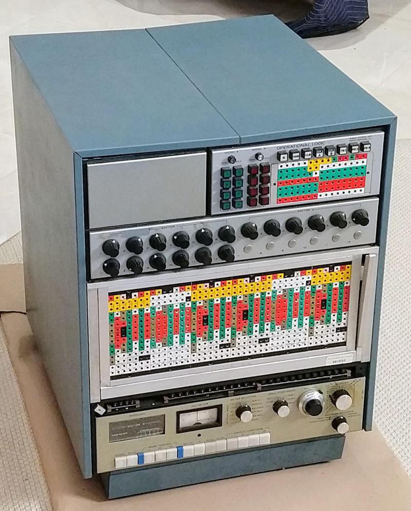
Multiplying two values, however, was surprisingly difficult; multiplication techniques were slow, inaccurate, noisy, or expensive. One accurate but slow multiplier used the Rube-Goldberg configuration of servo motors turning potentiometers.3 A 1969 multiplier circuit uses a light bulb and photocells. A fast and accurate approach was the "parabolic multiplier", built from numerous expensive high-precision resistors.4 The approach I'll discuss is to multiply by adding the logarithms and taking the exponential. Inconveniently, this approach magnifies even small differences between the transistors. It is also very sensitive to temperature. As a result, this approach was simple but inaccurate.

The Model 240 analog computer from Simulators, Inc. includes analog multipliers using the parabolic multiplier approach.

The Model 240 analog computer from Simulators, Inc. includes analog multipliers using the parabolic multiplier approach.

However, the development of analog integrated circuits created new opportunities for analog multiplication circuits. In particular, since the transistors in an integrated circuit were created together, they have nearly-identical properties. And the components on a tiny silicon die are all at nearly the same temperature.5

The first analog multiplier integrated circuit I could find is a television demodulator from 1967. The Gilbert cell technique was introduced by Barrie Gilbert in 1968 and is used in most analog multipliers today.6 The AD530 was introduced around 1970, and became an industry standard, but required external adjustments for accuracy. Laser-trimming the resistors inside the integrated circuit during manufacturing greatly improved the accuracy, an approach used in the AD633, the integrated circuit that was counterfeited.

Before explaining the circuitry of the RC4200 (the multiplier inside the counterfeit chip), I'll discuss the components that it is constructed from, and how they appear in an integrated circuit. This will help you recognize these structures in the die photo.

Transistors

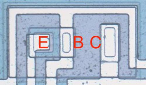
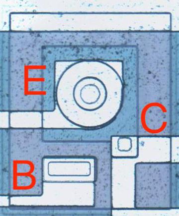
Transistors are the key components in a chip. The photo below shows an NPN transistor in the RC4200 as it appears on the chip. The different blue colors are regions of silicon that have been doped differently, forming N and P regions. The white lines are the metal layer of the chip on top of the silicon—these form the wires connecting to the emitter (E), base (B), and collector (C).

An NPN transistor on the RC4200 die. The emitter is embedded in the base, with the collector underneath.

An NPN transistor on the RC4200 die. The emitter is embedded in the base, with the collector underneath.

You might expect PNP transistors to be similar to NPN transistors, just swapping the roles of N and P silicon. But for a variety of reasons, PNP transistors have an entirely different construction. They consist of a circular emitter (P), surrounded by a ring-shaped base (N), which is surrounded by the collector (P). This forms a P-N-P sandwich horizontally (laterally), unlike the vertical structure of the NPN transistors. The diagram below shows one of the PNP transistors in the RC4200.

A PNP transistor has a circular structure.

A PNP transistor has a circular structure.

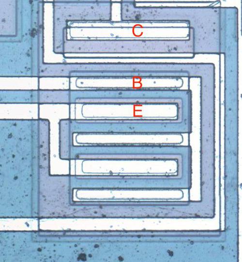
The input and output transistors in the RC4200 are larger than the other transistors and have a different structure to support higher currents. The photo below shows one of the output transistors. Note the multiple interdigitated "fingers" of the emitter and base.

A larger output transistor with parallel emitters and bases.

A larger output transistor with parallel emitters and bases.

Capacitors

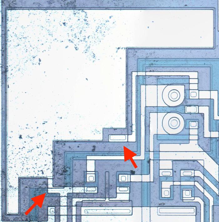
Capacitors are important in op amps to provide stability. A capacitor can be built in an integrated circuit as a large metal plate separated from the silicon by an insulating oxide layer. The main drawback of capacitors on ICs is they are physically very large. The 15pF capacitors in the RC4200 have a very small capacitance but take up a large fraction of the die area. In the photo below, the red arrows indicate the connection to the capacitor's metal layer and to the capacitor's underlying silicon layer.

The large metal area on the upper left is a capacitor.

The large metal area on the upper left is a capacitor.

Resistors

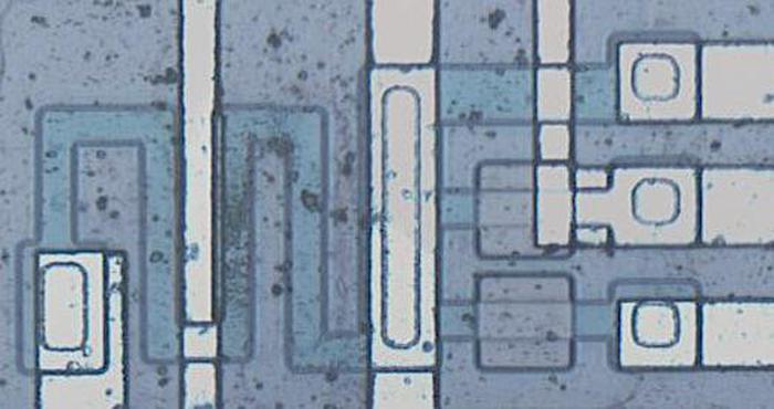
Resistors are a key component of analog chips. Unfortunately, resistors in ICs are very inaccurate; the resistances can vary by 50% from chip to chip. The photo below shows four resistors, formed using different techniques. The first resistor is the zig-zagging blue region on the left. It is formed from a strip of P silicon, with metal wiring (white) attached on the left and right. Its resistance is 3320 Ω. The resistor in the upper right is much shorter, so it is only 511Ω (long, narrow resistors have higher resistance than short, wide resistors). The remaining resistors are 20KΩ despite their small size because they are "pinch resistors". In the pinch resistor, the square layer of brownish N silicon on top makes the conductive region much thinner (i.e. pinches it). This allows a much higher resistance for a given size. (Otherwise, a 20 KΩ resistor would be 6 times as long as the first resistor, taking up excessive space.) The tradeoff is the pinch resistor is much less accurate.

Four resistors, one on the left and three on the right.

Four resistors, one on the left and three on the right.

Multiplying with logs and exponentials

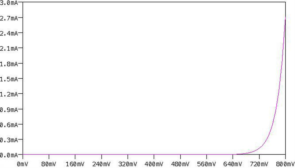
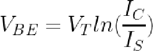
This integrated circuit multiplies using the log-antilog technique. The idea is that if you take the log of two numbers, add the logs together, and then take the antilog (i.e. exponential), you get the product of the two numbers. Conveniently, transistors have a logarithmic / exponential characteristic: the current through the transistor is an exponential of the voltage on the base. Specifically, if VBE is the voltage between the transistor's base and emitter, the current through the collector (IC) is an exponential of that voltage, as shown in the graph below. The analog multiplier takes advantage of this property.

Ic vs Vbe curve for a transistor, showing the exponential relationship. Generated by LTspice.

Ic vs Vbe curve for a transistor, showing the exponential relationship. Generated by LTspice.

The main complication with this approach is that the curve above is very sensitive to the temperature and to the manufacturing characteristics of the transistor. Because the curve is exponential, even a small shift in the curve will radically change the current. This was a serious difficulty when building a multiplier from discrete transistors, since the properties varied from transistor to transistor. To stabilize the temperature, some multipliers used a temperature-controlled oven. However, using an integrated circuit mostly solved these problems. The transistors in an integrated circuit are well-matched since they were built from the same piece of silicon under the same conditions. And the transistors in an integrated circuit die will be at almost the same temperature. Thus, integrated circuits made transistor-log circuits much more practical.

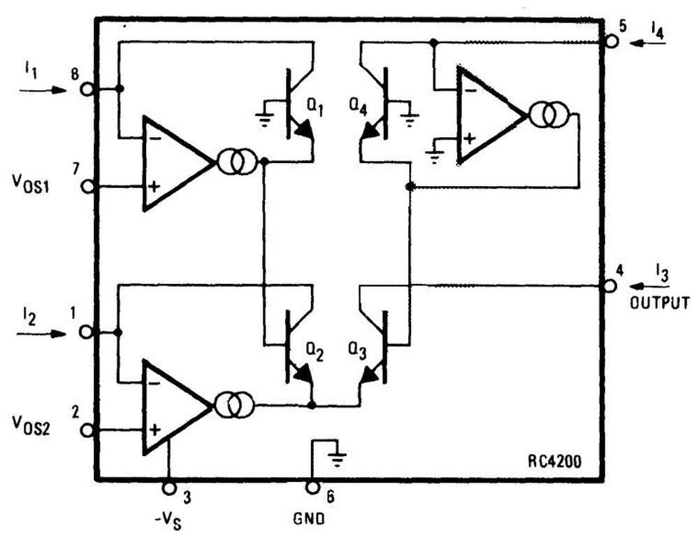
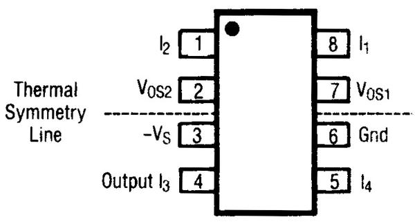
The diagram below shows the structure of the RC4200 multiplier chip. The user provides three current inputs (I1, I2, and I4) and the chip computes the output current I3, where I3 = I1×I2÷I4. (The use of current inputs and outputs is a bit inconvenient compared to other multipliers, such as the AD633, that use voltages.)

Structure of the RC4200 multiplier, from the datasheet. Note that the supply voltage (pin 3) is negative. VOS1 and VOS2 are offset adjustment pins to improve accuracy.

Structure of the RC4200 multiplier, from the datasheet. Note that the supply voltage (pin 3) is negative. VOS1 and VOS2 are offset adjustment pins to improve accuracy.

The four transistors in the middle of the diagram are the multiplier core, the key to the IC's operation. The transistors are configured so their base-emitter voltages sum: VBE3 = VBE1+VBE2-VBE4. Because the transistor current is related exponentially to the voltage, the result is that I3 = I1×I2÷I4.

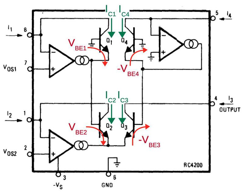
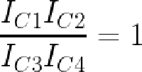
In more detail, first note that the voltages VBE1 through VBE4 control the collector currents IC1 through IC4 through the transistors (below). The op amps adjust the base-emitter voltages so the input currents match the transistor currents, i.e. I1 = IC1 and so forth. (This is accomplished by op amp feedback.) Now, if you go through the loop of base-emitter voltages starting at the base of Q1 and ending at the base of Q4 (red arrows), you find that VBE1+VBE2-VBE3-VBE4 = 0. (The voltages must sum to zero since you start at ground and end at ground.7) Now, because IC is related to exp(VBE), taking the exponential of the equation yields IC1×IC2÷IC3÷IC4 = 1. (Details in footnote8.)

Traveling around the loop indicated by the arrows, the voltages must sum to 0.

Traveling around the loop indicated by the arrows, the voltages must sum to 0.

Next, I'll explain how the VBE voltages are generated. Each current input has an op amp associated with it that produces the "correct" VBE voltage for the current using a feedback loop9 For example, suppose IC is too low so not all the input current flows through the transistor. The excess current will raise the voltage on the op amp's negative input, causing it to reduce its output voltage and thus the transistor's emitter voltage. This raises VBE (since the base will now be higher compared to the emitter), causing more collector current to flow through the transistor. Similarly, if too much current is flowing through the transistor, the op amp's input will be pulled lower, reducing VBE. Thus, the feedback loop causes the op amp to find the exact VBE for the current input.10

Correcting for emitter resistance

The above circuit works reasonably well, but there's a complication: the transistors have a small emitter resistance R. The voltage drop across this resistance will increase VBE by ICR, disturbing the nice exponential behavior. This creates a nonlinearity that reduces the accuracy of the result. The datasheet says that "Raytheon has developed a unique and proprietary means of inherently compensating for this undesired term." They don't explain this further, but by studying the die I have figured out how it works.

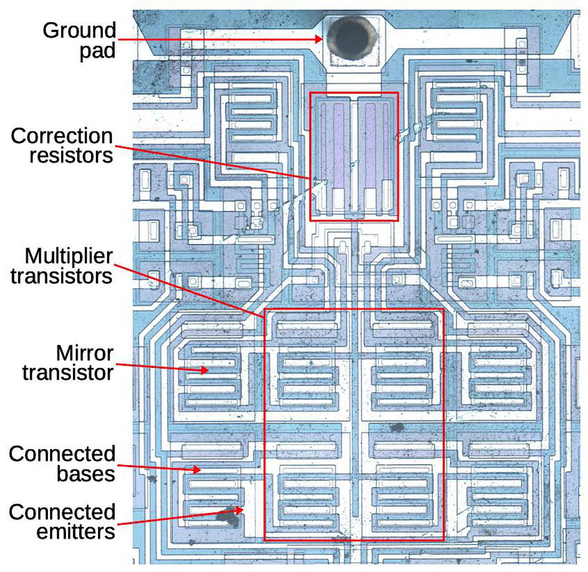
In the compensation circuit, each of the four multiplier transistors is paired with an identical "mirror" transistor with the corresponding emitters and corresponding bases connected, as shown below. These connections give the paired transistors the same base and emitter voltages, so they have the same collector currents. In other words, they form a current mirror. The mirrored currents are fed into special correction resistors that match the undesired emitter resistance, 0.1 Ω according to the datasheet.11 The voltage across the correction resistors will be the same as the excess voltage that needs to be compensated (since the resistance and current are the same). The final step is the correction resistors are connected to the base of the multiplication transistors, replacing the connection to ground. This will shrink VBE by the amount it was erroneously increased, fixing the computation.

The main multiplier consists of four transistors. Each transistor has a mirror transistor generating the same current, used to correct for emitter resistance.

The main multiplier consists of four transistors. Each transistor has a mirror transistor generating the same current, used to correct for emitter resistance.

Why are there two correction resistors? Recall that the multiplier has two transistors adding and two transistors subtracting (i.e. VBE1+VBE2-VBE3-VBE4 = 0). To handle this, the correction circuit is split in two. The left half sums IC1 and IC2 and applies this current to a correction resistor on the Q3/Q4 side, while the right half sums IC3 and IC4 and applies this to a correction resistor on the Q1/Q2 side. The addition and subtraction work out to yield the desired net correction.

Schematic

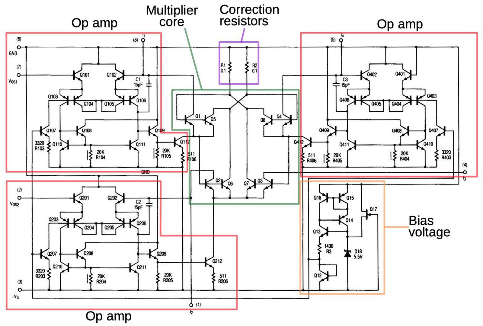
The schematic below shows the complete circuitry of the RC4200; I've highlighted the main functional blocks. (Inconveniently, I didn't find this schematic until after I'd traced out the circuitry from the die photo.) The multiplier core and the correction resistors were discussed above The op amps circuits are fairly similar to the 741 op amp, which I've written about. They lack the output stage of typical op amps; the output transistor (Q112/Q212/Q412) corresponds to the intermediate gain state in a typical op amp. The bias circuit (orange, lower right) provides a fixed bias voltage for the op amps.12

Schematic from the datasheet, with main functional groups labeled.

Schematic from the datasheet, with main functional groups labeled.

Conclusion

Before integrated circuits, analog multiplication was difficult to implement. However, integrated circuits made it easy to create matched transistors, leading to fast, inexpensive analog multiplication integrated circuits. Unfortunately, analog multiplier integrated circuits were introduced just as analog computers were dying out, killed by inexpensive digital microprocessors, so analog computing missed most of the benefit of these chips.

While most analog multipliers use a circuit called the Gilbert cell, the Raytheon RC4200 analog multiplier uses a different technique to multiply and divide values represented by currents. Although, it includes a special error compensation circuit to improve its accuracy, it is obsolete compared to accurate, laser-trimmed multipliers. Now, counterfeiters re-label RC4200 chips and sell them as the more-expensive AD633 multiplier.

Die photo of the RC4200, courtesy of John McMaster.

Die photo of the RC4200, courtesy of John McMaster.

I announce my latest blog posts on Twitter, so follow me at kenshirriff for updates. I also have an RSS feed. Thank you to John McMaster for the die photos used in this blog post; the photos are here.

Notes and references

  1. One reason that the AD633 multiplier is so expensive is that the resistors on the die are laser-trimmed resistors for accuracy. To get an accurate result, an analog multiplier requires exactly-tuned resistances. The older RC4200 requires adjustable external resistors, which is much less convenient. 

  2. I'm a bit puzzled by this counterfeit chip. Sometimes people will label a cheap op amp as an expensive op amp, as explained by Zeptobars. At first glance, that's what's going on here: a cheap multiplier repackaged as an expensive one. However, the two multipilers are so different that I can't imagine one working at all in place of the other. Specifically, the AD633 takes differential voltage inputs and outputs two currents (a differential current), and it computes A×B+C. The RC4200, on the other hand, takes current inputs and outputs a single current, and it computes A×B÷C. 

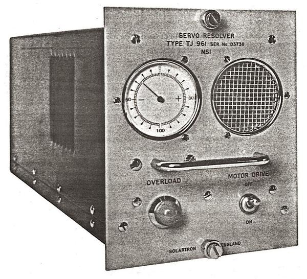
  3. An example of a servo multiplier is the Solartron Servo Multiplier from the late 1950s. This 17-pound unit contained a potentiometer controlled by a servo motor, allowing it to multiply numbers represented by +/- 100 volts. It's surprisingly fast considering its mechanical operation, responding in under 30 milliseconds. Power consumption was high: 70 watts, cooled by a fan. (In comparison, the RC4200 chip uses 40 milliwatts of power.)

    This photo shows the Solartron TJ961 Servo Resolver. This implements multiplication as well as sine/cosine computation. Photo from manual via Analog Museum.

    This photo shows the Solartron TJ961 Servo Resolver. This implements multiplication as well as sine/cosine computation. Photo from manual via Analog Museum.

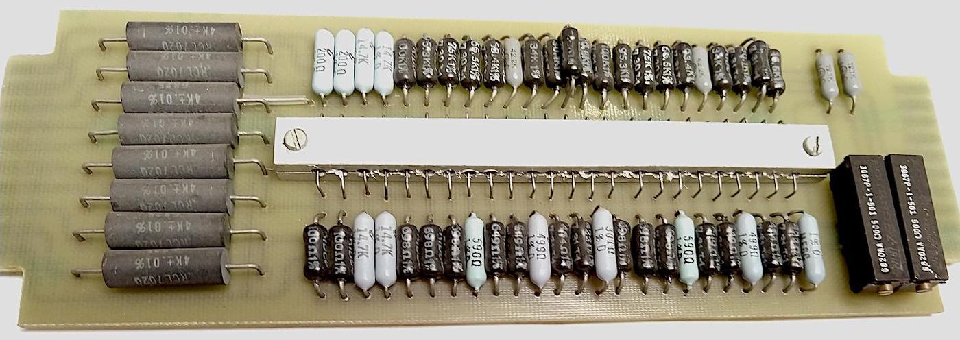
  4. The 1969 analog computer I'm restoring uses a parabolic multiplier, a technique used for high-accuracy multiplication. The idea is that to compute A×B, you compute ((A+B)^2 - (A-B)^2)/4, which has the same value. That equation looks much more complex than the original product, but is easier to implement on an analog computer because op amps can perform the sums, subtraction, and division by four. Squaring is easier than multiplication because it is a function of a single variable, so it can be implemented by an "arbitrary function generator".

    Parabolic multiplier circuit board from a Simulators, Inc. 2400 analog computer.

    Parabolic multiplier circuit board from a Simulators, Inc. 2400 analog computer.

    The photo above shows a function board from an analog computer that computes the square, i.e. a parabola. The board approximates the function by multiple piecewise-linear segments, each defined by resistors. (Note the extremely accurate 0.01% resistors on the left.) The metal block in the center holds diodes, temperature-balanced by the metal. Each diode is biased to turn on at a particular voltage; the diodes act as switches, selecting the appropriate resistors for each linear segment. Note the large amount of precision hardware required for multiplication; a single product requires two of these parabolic function boards as well as multiple op amps. 

  5. To minimize the effect of temperature on the integrated circuit, the critical multiplier transistors are placed close together in the center of the chip. If there is a thermal gradient across the chip, this will minimize the temperature difference between the transistors. (Compared to putting the transistors in the corners, for instance.) To reduce temperature gradients even more, the datasheet specifies a "thermal symmetry line". Putting a temperature source on this line ensures that the hotter transistors will tend to cancel each other out.

    The datasheet shows the IC's thermal symmetry line.

    The datasheet shows the IC's thermal symmetry line.

  6. Barrie Gilbert, inventor of the Gilbert cell, has a video explaining translinear circuit, circuits based on the exponential current-voltage relationship of a bipolar transistor. This video explains translinear analog multipliers in detail, discussing two approaches> The first approach, used by the RC4200, is the "log-antilog" approach, where op-amps force and sense the collector currents. The second, used in the AD633 and many other multipliers, is the "integrated" approach, built from voltage-to-current conversion, a differential current-mode core, and current-to-voltage conversion. 

  7. I should mention that the chip uses a -15 V supply, so ground is the highest voltage and the other internal voltages are all negative. Just a warning since this makes things confusing and backward compared to circuits where ground is the low voltage. 

  8. The relationship between the base voltage and the collector current is given by the Ebers-Moll model. This equation (below) is filled with interesting constants: α: a gain factor (almost 1), k: the Boltzmann constant, IS: the saturation current (extremely small, order of 10-15 A), T: the absolute temperature, q: the charge on the electron. (The temperature in the exponential term reflects the importance of temperature stability for the multiplier.)

    Substituting the thermal voltage VT (about 26 mV) for kT/q, making some minor approximations, and taking the log yields:

    Substituting that into the multiplier's VBE loop equation yields

    Taking the exponential and assuming the transistors all have the same temperature and saturation current yields the desired equation relating the four currents:

    This equation shows how the four currents are related by multiplication and division. See the datasheet for more details. 

  9. In a sense, the op amps compute the inverse of the transistor's exponential function. The transistor takes VBE as an input and produces the exponential current as an output. However, we have the current as the input and want the logarithmic voltage as the output. By using the op amp with a function in its feedback loop, we can find the inverse of a function, in this case giving us the logarithm. That is, the op amp will converge on the output X where f(X) equals the input, i.e. X = f-1</sup(input). The same technique can be used to generate a square root from a multiplier chip: use the multiplier to square its input, and then use an op amp to compute the inverse function, i.e. the square root. 

  10. You might wonder why the op amp finds the "correct" value and doesn't overshoot and oscillate. Handwaving away all the theory, the idea is that the capacitor on the op amp input stabilizes it and prevents oscillation. Even so, the datasheet warns that the circuits become unstable as the input currents approach 0. This corresponds to dividing by zero, so it's not surprising that the circuitry doesn't handle it well. Mathematically, the op amp is trying to find ln(0), which isn't going to work. If you want to multiply by zero or negative values, the datasheet describes how the inputs can be biased with resistors to keep the inputs positive but still get the correct answer. 

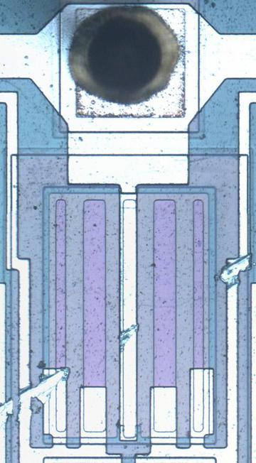
  11. The two resistors below are used for the emitter correction; they have unusual construction and a very small resistance, 0.1 Ω. Each resistor consists of the two vertical stripes, connected together at the bottom; the vertical region in the center is connected to the ground pin, forming the other side of each resistor. These resistors improve the accuracy of the product by correcting for the emitter resistances. Based on their purple color, which doesn't appear elsewhere on the die, they appear to be specially doped. The metal contacts at the bottom cover part of the resistor; I believe that by adjusting the size of the metal contacts, the resistor values can be tuned. I believe that the thick and thin regions allow for coarse and fine tuning.

    Precise small-valued resistors provide a correction factor.

    Precise small-valued resistors provide a correction factor.


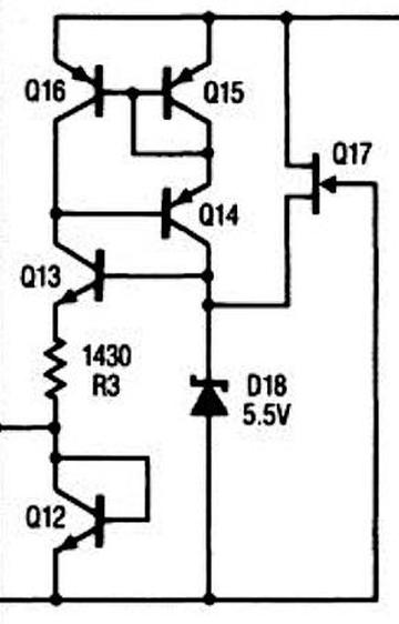
  12. The bias voltage circuit generates a stable voltage of one diode drop (about 800 mV) from Q4's collector; this voltage biases the op amps. The tricky part is how to keep the power supply voltage from influencing this voltage or the Zener voltage.

    The bias generation circuit, from the datasheet.

    The bias generation circuit, from the datasheet.

    The idea is that the Zener diode puts 5.5 volts on the base of Q13. The voltage across R3 will be two diode drops lower (2.8 V) due to Q13 and Q12. This yields a fixed current of 2.8 V / 1430 Ω = 2 mA through Q4, resulting in a stable voltage drop across Q12 and a stable output. But a Zener's voltage fluctuates a bit with current, so the clever part is how the Zener's current is kept stable. Transistors Q14, Q15, and Q16 form a current mirror, so the current through the Zener will match the current through the resistor, which is 2 mA. Thus, the Zener voltage keeps the resistor current and output voltage stable, while the resistor current keeps the Zener stable. The final piece of the puzzle is the FET Q17, which provides a tiny current through the Zener to start the feedback cycle. 

HP Nanoprocessor part II: Reverse-engineering the circuits from the masks

In 1974, Hewlett-Packard developed a microprocessor for control applications in their products, from floppy disk drives to voltmeters. This simple processor was a step down from the typical microprocessor—it didn't even support addition or subtraction1—so it was called the Nanoprocessor. The Nanoprocessor's key features were its low cost and high speed: compared against the contemporary Motorola 6800, the Nanoprocessor cost $15 instead of $360 and performed control tasks an order of magnitude faster.

This processor remained obscure for decades until its designer, Larry Bower, recently donated the chip's masks and documentation to The CPU Shack, who scanned the masks and wrote about the Nanoprocessor. After Antoine Bercovici stitched together the images,2 I wrote a Nanoprocessor overview article based on them. This blog post is part two, where I discuss some of the Nanoprocessor circuitry in detail, reverse-engineering it from the masks. These functional blocks are interesting to study because the Nanoprocessor strips its implementation down to the minimum, while still remaining a useful microprocessor.

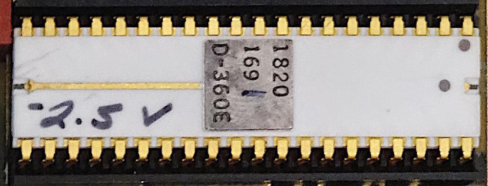
The HP Nanoprocessor, part number 1820-1691. Note the hand-written bias voltage "-2.5 V", which varies from chip to chip. The last digit (1) of the part number is also hand-written, indicating
the speed of the chip. Photo courtesy of Marc Verdiell.

The HP Nanoprocessor, part number 1820-1691. Note the hand-written bias voltage "-2.5 V", which varies from chip to chip. The last digit (1) of the part number is also hand-written, indicating the speed of the chip. Photo courtesy of Marc Verdiell.

Inside the Nanoprocessor

Like most processors of that era, the Nanoprocessor was an 8-bit processor. However, it didn't support RAM,3 but ran code from an external 2-kilobyte ROM. It contained 16 8-bit registers, more than most processors and enough to make up for the lack of RAM in many applications. The Nanoprocessor had 48 instructions, a considerably smaller instruction set than the Motorola 6800's 72 instructions. However, the Nanoprocessor included convenient bit set, clear, and test operations, which other processors of that era lacked. It also had multiple I/O instructions supporting both I/O ports and general-purpose I/O pins, making it easy to control devices with the Nanoprocessor.

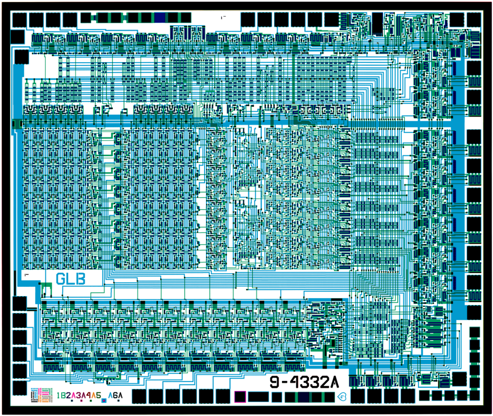
Combined masks from the Nanoprocessor. Click for larger image. Files courtesy of Antoine Bercovici using scans from The CPU Shack.

Combined masks from the Nanoprocessor. Click for larger image. Files courtesy of Antoine Bercovici using scans from The CPU Shack.

The mask image above shows the simplicity of the Nanoprocessor. The blue lines show the metal wiring on top of the chip, while the green shows the doped silicon underneath. The black squares around the outside are the 40 pads for connection to the IC's external pins. The small black regions inside the chip are transistors; if you squint, you should be able to count 4639 of them.4

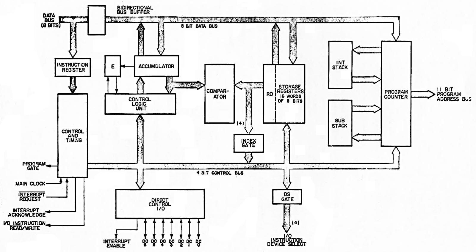
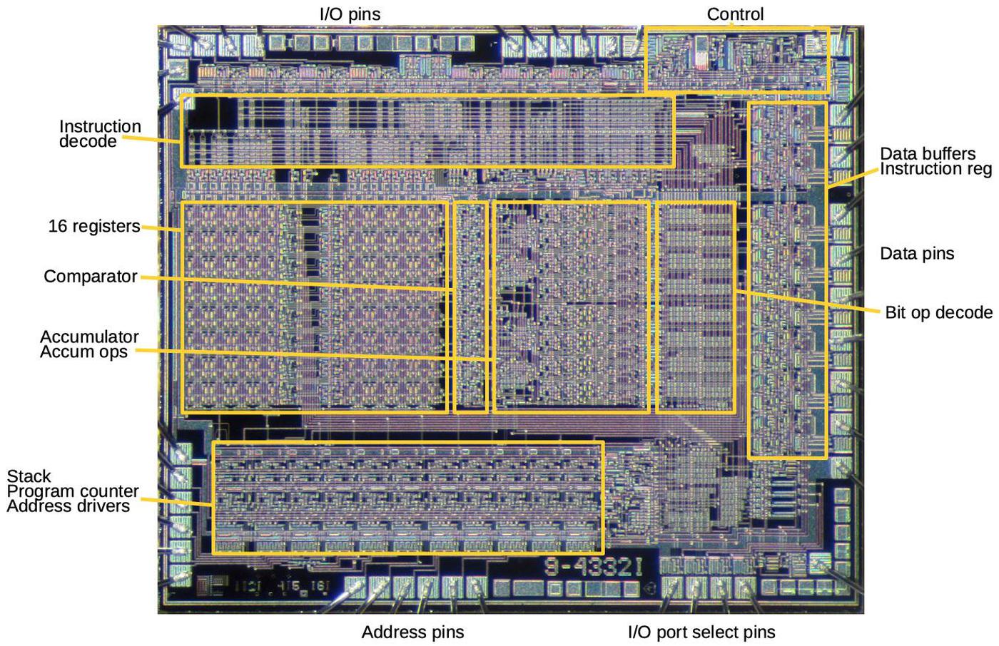
The block diagram below shows the internal structure of the Nanoprocessor. The 16 storage registers are in the middle. The comparator allows two values to be compared for conditional branches. The Control Logic Unit performs increments, decrements, shifts, and bit operations on the accumulator, lacking the arithmetic and logical operations of a standard Arithmetic/Logic Unit (ALU). The program counter (right) fetches an instruction into the instruction register (left); interrupts and subroutine calls each have a one-entry stack for the return address.

Block diagram, from the Nanoprocessor User's Guide.

Block diagram, from the Nanoprocessor User's Guide.

I should emphasize that despite its simplicity5 and lack of arithmetic, the Nanoprocessor is not a "toy" processor that just toggles some control lines, but a fast and capable processor used for complex tasks. The HP 98035 real-time clock module, for instance, uses the Nanoprocessor to parse two dozen different ASCII command strings, as well as activities such as calculating the number of days in each month.

Registers

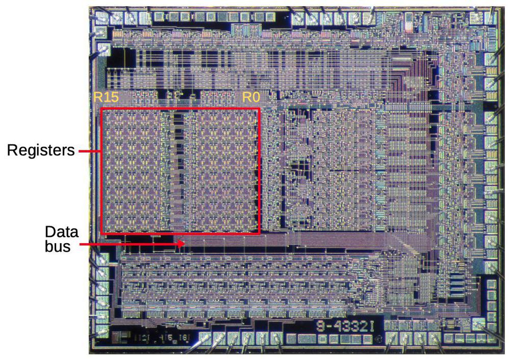
The die photo below shows that much of the Nanoprocessor's die is occupied by its 16 registers. These registers communicate with the rest of the chip via the data bus. Circuitry above the registers selects a particular register. Register R0, on the right, is next to the comparator, which will be important later.

The registers take up a large fraction of the Nanoprocessor's die.
Underlying die photo by Pauli Rautakorpi, CC BY 3.0.

The registers take up a large fraction of the Nanoprocessor's die. Underlying die photo by Pauli Rautakorpi, CC BY 3.0.

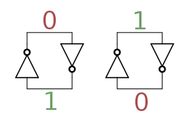
The building block for the registers is two inverters in a feedback loop, storing a single bit as shown below. If the top wire has a 0, the right inverter will output a 1 to the bottom wire. The left inverter will then output a 0 to the top wire, completing the cycle. Thus, the circuit is stable and will "remember" the 0. Likewise, if the top wire is a 1, this will get inverted to a 0 at the bottom wire, and back to a 1 at the top. Thus, this circuit can store either a 0 or a 1, forming a 1-bit memory.

Two inverters implement a stable loop that stores a bit.

Two inverters implement a stable loop that stores a bit.

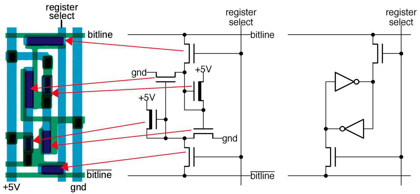
The diagram below shows how this two-inverter storage is implemented on the die. The left shows the physical layout, from the mask images. The layout is optimized to make the cell as small as possible. Blue lines indicate the metal layer, while green is the silicon layer. The schematic in the middle shows the corresponding transistor circuitry. Each inverter is formed from a pair of transistors, as shown on the right. The top and bottom transistors are "pass transistors", providing access to the storage cell.

One bit of storage in the Nanoprocessor. Each bit is implemented by 6 transistors (also known as a 6T SRAM cell).

One bit of storage in the Nanoprocessor. Each bit is implemented by 6 transistors (also known as a 6T SRAM cell).

The register set is built from a matrix of these bit cells. The register select line selects one register (one column) for reading or writing. When selected, the top and bottom pass transistors connect the inverters to the corresponding horizontal bitlines. For a read operation, the top bitline provides the value stored in the cell; there are eight pairs of bitlines for the eight bits in a register. For a write operation, the value is applied to the upper bitline and the inverted value is applied to the lower bitline. These values overpower the signals from the inverters, forcing the inverters to the desired value and storing the bit. Thus, the grid of horizontal bitlines and vertical select lines allows a particular register to be read or written.

Instruction decoding

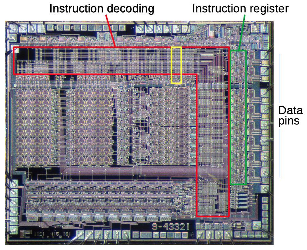
The instruction decoding circuitry is responsible for taking a binary instruction code (such as 01101010) and determining what instruction it is ("Load accumulator from register 10" in this case). Compared to many processors, the Nanoprocessor's instructions are pretty simple: it has relatively few instructions (48) and the opcode is always one byte long. The diagram below shows that instruction decoding logic (red) takes up a large fraction of the chip. The instruction register (green), is a set of eight latches holding the current instruction. The instruction register is next to the data pins, which provide the instruction from the ROM. This section will focus on the decoding circuit in the yellow box.

A large part of the chip is devoted to instruction decoding (red). This section will focus on the circuit highlighted in yellow. Underlying die photo by Pauli Rautakorpi, CC BY 3.0.

A large part of the chip is devoted to instruction decoding (red). This section will focus on the circuit highlighted in yellow. Underlying die photo by Pauli Rautakorpi, CC BY 3.0.

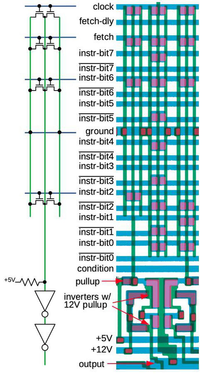
Decoding is done by NOR gates; each NOR gate detects a particular instruction or group of instructions. The NOR gates take instruction bits or their complements as inputs. When all inputs are zero, the NOR gate indicates a match. This allows matching against the entire instruction or part of the instruction. For instance, the "Load accumulator from register R" instruction has the binary format "0110rrrr", where the last four bits indicate the desired register. A NOR gate (bit7 + bit6' + bit5' + bit4)' will match instructions of that form.

The nice thing about structuring the instruction decoder in this way is that it can be built from compact, regular circuits, often called a PLA.6 The idea is to make a matrix with input signals running horizontally and outputs vertically. Each intersection can have a transistor, making the input signal part of the gate; or no transistor, ignoring that input signal. The result is tightly-packed NOR gates.

The diagram on the right below zooms in on the three decoders highlighted in yellow above. The schematic corresponds to the leftmost decoder; note the correspondence between transistors in the schematic and the pink transistor blobs in the layout. The idea is that if any input energizes a transistor, the transistor will pull the output to ground. Otherwise, the output is pulled high by the resistor. The inverters at the bottom amplify the signal, providing enough current to drive all eight slices of the accumulator.7 Curiously, the layout uses pairs of transistors, both connected between ground and the output; I don't see the advantage over the straightforward approach of using a single transistor. In any case, note how the PLA-style matrix provides a dense layout for the decoders.

This diagram shows one of the decoder circuits in the Nanoprocessor. The schematic corresponds to the leftmost decoder of the three shown on the right.

This diagram shows one of the decoder circuits in the Nanoprocessor. The schematic corresponds to the leftmost decoder of the three shown on the right.

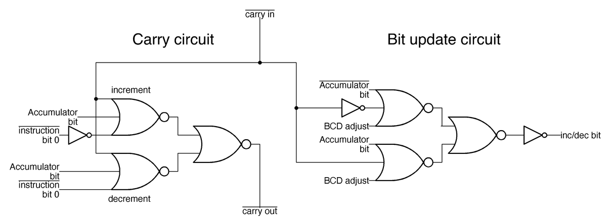
This particular circuit generates the increment/decrement signal that is fed into the accumulator circuit. This circuit matches when the clock, fetch, instruction bit 6, and instruction bit 2 are all low, so it matches instructions of the form x0xxx0xx during execute phase. These instructions include "Increment Binary" (00000000), "Increment BCD" (00000010), "Decrement Binary" (00000001) and "Decrement BCD" (00000011).8

Comparator

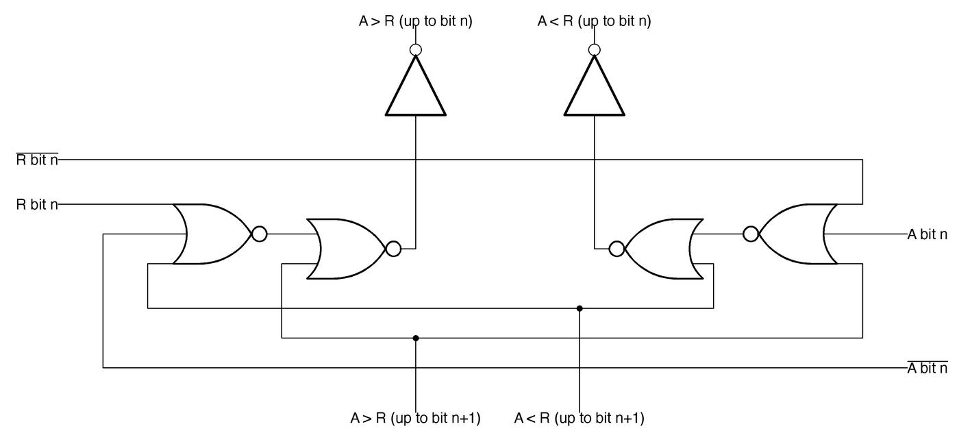
An important circuit in the Nanoprocessor is the comparator that determines if the accumulator A is greater, less than, or equal to register R0. The comparator uses a simple but clever circuit to compare these two values. The algorithm is essentially to compare the two numbers starting with the most significant bits. As long as the bits are equal, keep moving to the less significant bits. The first difference between the two numbers determines which one is greater. (For instance, with 10101010 and 10100111, the highlighted bits determine that the first number is greater.)

This algorithm is implemented with eight stages, one for each bit, starting with the most significant bits at the bottom. Each stage (below) consists of two symmetrical parts: one determines if A > R0, while the complementary one determines if A < R0. If the numbers are equal so far, but the two bits are different at this stage, the stage generates the greater than or less than signal. Otherwise, it passes along the decision of the lower stage. The topmost stage outputs the final decision. Note that the comparator provides an equality test "for free"; if the output isn't greater than or less than, the two numbers are equal.

One stage of the 8-bit comparator.

One stage of the 8-bit comparator.

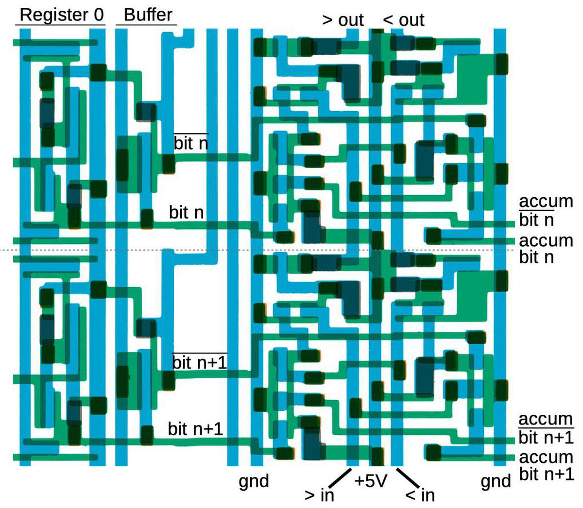
The diagram below shows the physical layout of two comparator stages. One clever feature of the comparator's layout is that it sits between register 0 on the left and the accumulator on the right, minimizing wiring. The comparator accesses register 0 directly, without going through the regular path of the register selection and the data bus.

Two stages of the comparator, as it appears in the masks.

Two stages of the comparator, as it appears in the masks.

The Nanoprocessor's conditional branch instructions can test the comparator outputs.9 The branch circuitry is fairly straightforward: several bits of the branch instruction select the particular test via a multiplexer. Then bit 7 of the instruction selects "branch if true" versus "branch if false". Unlike most processors, the Nanoprocessor doesn't provide branches to an arbitrary address. Instead, it skips two instruction bytes if the condition is satisfied. (Typically these two bytes would hold a jump to the desired target, but sometimes hold other instructions.) The skip circuit is simple: the program counter incrementer (described below) is triggered a second time, but increments by two instead of one, skipping two instructions. Thus, the Nanoprocessor implements an extensive set of conditional tests with a relatively small amount of circuitry.

Accumulator and Control Logic Unit

The accumulator is the special 8-bit register that stores the byte currently being processed. Operations on the accumulator are performed by the Control Logic Unit (CLU), which the manual calls "the heart of the Nanoprocessor". The CLU is the equivalent of the Arithmetic/Logic Unit (ALU) in most processors, except it doesn't perform arithmetic or logic operations. The CLU is not quite as useless as it sounds, though. It can increment or decrement the accumulator, both in binary and binary coded decimal (BCD). (Binary coded decimal stores two decimal digits per byte. This is very useful for decimal I/O or displays.) The CLU can also complement or clear the accumulator, or set or clear a specific bit. Finally, it supports left and right shift operations.

Circuitry related to the accumulator.
Underlying die photo by Pauli Rautakorpi, CC BY 3.0.

Circuitry related to the accumulator. Underlying die photo by Pauli Rautakorpi, CC BY 3.0.

The diagram above shows the layout of the accumulator and CLU. The first region has miscellaneous circuitry to detect a zero value; support BCD by detecting a 9 digit, for instance; and provide carry-skip, fast carry generation from the lower 4 bits. I won't discuss this in more detail, but note the irregular layout of this circuitry. The second region holds the main accumulator and CLU circuitry; I will discuss this in detail below. The third region distributes control signals from the decode logic above to the eight accumulator slices. Finally, the last region holds instruction decoding logic to decode bit operations and signal the appropriate accumulator slice.

The main part of the accumulator/CLU consists of 8 slices, one for each bit, with the lowest bit at the top. I will discuss four circuits in each slice: the incrementer/decrementer's carry generation, the incrementer/decrementer's bit generation, the multiplexer to select the new accumulator value, and the latch that holds the accumulator's value.

Each slice of the incrementer/decrementer (below) is implemented by a half adder. The direction of the incrementer/decrementer circuit depends on the opcode: a 0 in the opcode's low bit indicates an increment, while a 1 in the opcode's low bit indicates a decrement. The carry circuit on the left below generates the carry-out signal. For an increment, there is a carry-out if there is a carry-in and the current bit is 1 (since it will be incremented to binary 10). For decrement, the carry line indicates a borrow, rather than a carry, so there is a carry-out if there is a carry-in (i.e. a borrow) and the current bit is 0, triggering a borrow.

One slice of the incrementer/decrementer circuit.

One slice of the incrementer/decrementer circuit.

The circuit on the right above updates the current bit when incrementing or decrementing. The current bit is flipped if there is a carry-in, essentially an XOR implemented by three NOR gates. One complication is the adjustment for BCD (binary-coded decimal). For a BCD increment operation, a carry occurs when incrementing a 9 digit, while for a BCD decrement, a 0 digit is decremented to 9, not to binary 1111.

The different accumulator operations are provided by the multiplexer below. Depending on the operation, one pass transistor will be activated, selecting the desired value. For instance, for an increment/decrement operation, the top transistor selects the output from the increment/decrement circuit described above. This transistor is activated by the instruction decoder described earlier that matches an increment/decrement instruction. Similarly, a shift-right instruction activates the shift-right pass transistor, feeding accumulator bit n+1 into each accumulator slice to shift the value.

Schematic of the latch holding one bit of the accumulator, along with the multiplexer that selects an input to the accumulator.

Schematic of the latch holding one bit of the accumulator, along with the multiplexer that selects an input to the accumulator.

The latch above stores one bit of the accumulator. When the hold accumulator transistor is activated, the two NOR gates form a loop, holding the value. But when the load accumulator transistor is activated instead, the accumulator loads its value from the multiplexer. The clear bit n and set bit n lines allow instructions to modify individual bits of the accumulator; the multiplexer, in comparison, updates all accumulator bits at once.

Program counter and addressing

Another large block of circuitry is the 11-bit program counter in the lower left of the Nanoprocessor, which I'll describe briefly. This block also includes a latch to hold the return address for a subroutine call and a second latch to hold the program counter after an interrupt. (You can think of these as one-entry stacks.) The program counter includes an incrementer to advance it to the next instruction. This incrementer can also increment by two, allowing conditional branch instructions to skip over two instructions. (Increment-by-two is implemented by incrementing bit 1 instead of bit 0.) To improve the performance of the incrementer, it has a carry-skip feature; if the bottom six bits are all 1, it will increment bit 6 immediately without waiting for the carry to propagate through the low-order bits.

Control and timing

The final piece of the Nanoprocessor is the control circuitry. Compared to other microprocessors, the Nanoprocessor's control circuitry is almost trivial: the processor alternates between fetch and execute cycles (with the occasional interrupt). The control circuitry is not much more than a couple of flip flops and gates, so I won't say more about it.

Conclusions

The diagram below summarizes the main functional blocks of the Nanoprocessor. The Nanoprocessor achieves a dense layout for these blocks, much better than I would expect from its obsolete metal-gate technology.10 Reverse-engineering shows that these functional blocks are implemented with simple but carefully-designed circuits.

Functional components of the HP Nanoprocessor, based on my reverse-engineering.
Underlying die photo by Pauli Rautakorpi, CC BY 3.0.

Functional components of the HP Nanoprocessor, based on my reverse-engineering. Underlying die photo by Pauli Rautakorpi, CC BY 3.0.

The Nanoprocessor is an unusual processor. My first impression was that it wasn't even a "real processor," since it lacked basic arithmetic functionality. However, after studying it, I'm more impressed. Its simple design allows it to operate faster than other processors of the time. The instruction set is more capable than it appears at first. Hewlett-Packard used the Nanoprocessor in many products in the 1970s and 1980s, in roles that were more complex than you'd expect, such as parsing strings and performing calculations. Now, with the masks released by The CPU Shack, we can learn the secrets of the circuits that made the Nanoprocessor work.

Nanoprocessor (white chip) as part of an HP clock module.
Note the hand-written voltage on the chip; each chip required a different bias voltage.
Photo courtesy of Marc Verdiell.

Nanoprocessor (white chip) as part of an HP clock module. Note the hand-written voltage on the chip; each chip required a different bias voltage. Photo courtesy of Marc Verdiell.

Follow me on Twitter at @kenshirriff for updates on my blog posts. I also have an RSS feed. Thanks to Antoine Bercovici for scanning and remastering the masks, Larry Bower for the donation, and John Culver at The CPU Shack for sharing the donation.

Notes and references

  1. Although it lacks an addition instruction, the Nanoprocessor can add numbers (slowly) through repeated increment and decrement operations (which it supports). (The code for the HP real-time clock module does this.) Other applications, such as the HP voltmeter, added external ALU chips (74LS181) to perform fast addition; these were accessed as I/O devices. (With Turing-completeness, of course, the Nanoprocessor can theoretically do anything from floating-point functions to Crysis; it will just be very slow.) 

  2. The mask images can be downloaded here (warning: 122 MB PSD file). 

  3. The Nanoprocessor doesn't have instructions to support RAM, since it is designed for control applications that typically don't need much storage. However, some Nanoprocessor applications use RAM, treating RAM as an I/O device. The address is written to one I/O port and the data byte is read or written from another port. 

  4. By my count, the Nanoprocessor has 4639 transistors. The instruction decoder is constructed from pairs of small transistors for layout reasons; combining these pairs yields 3829 unique transistors. Of these, 1061 act as pull-ups, while 2668 are active. In comparison, the 6502 has 4237 transistors, of which 3218 are active. The 8008 has 3500 transistors and the Motorola 6800 has 4100 transistors. 

  5. Making an FPGA version of the Nanoprocessor would probably be a fun project since the Nanoprocessor is about as simple as you can make a real, commercial processor. The User's Guide explains the instructions and has sample code that could be executed. 

  6. Building the decoder out of an array of NOR gates decoding was common in early microprocessors, for instance the 6502, because it could be constructed in a regular, compact form. It's often called a PLA (Programmable Logic Array), even though a PLA is supposed to have two layers of logic. 

  7. Note that the inverters in the instruction decoder are pulled up to 12 volts, rather than 5 volts. The reason is that the Nanoprocessor uses metal-gate transistors, rather than the more advanced silicon-gate transistors of other microprocessors of the era. Metal-gate transistors have the disadvantage of a higher threshold voltage, which means the output of a transistor is considerably lower than the gate voltage. The output from a regular inverter is too low to drive the gate of a pass transistor, since the output will be another threshold voltage below that. The solution is to use the 12 volt supply for the decoder inverters that drive pass transistors in the accumulator. Then, these signals have plenty of voltage to drive pass transistors. In other words, the Nanoprocessor required an extra +12V supply because it used metal-gate transistors instead of the more modern silicon-gate transistors. 

  8. The illustrated decode circuit matches against instructions x0xxx0xx, so it matches against many more instructions than just the increment and decrement instructions. Why doesn't the circuit match exactly? The reason is that if the accumulator is not being used, it doesn't matter if the increment/decrement signal is activated. By making the match wider, the designers could omit some transistors. The important point is that the circuit rejects other accumulator instructions such as "Clear accumulator" (00000100) or "Load accumulator from register" (0110rrrr). 

  9. The Nanoprocessor has an extensive set of conditional branches, surprisingly many for a simple processor. You can branch if A > R0, A >= R0, A < R0, A <= R0, A == R0, or A != R0. In additional conditional branches can be done on the accumulator being zero or nonzero, any particular bit of the accumulator being zero or nonzero, the overflow flag being set or not, or a particular general-purpose I/O ("direct control") bit being set or not. 

  10. The Nanoprocessor used metal-gate transistors, while other microprocessors started using silicon-gate transistors a few years earlier. This may seem like an obscure difference, but it has a huge impact on layout: silicon-gate fabrication added a layer of polysilicon wiring. This makes layout much easier, since you now have two layers for wiring that can cross each other. With just the metal layer for wiring, like the Nanoprocessor, layout is difficult because wires keep getting in the way of each other. In other metal-gate chips that I've examined, the layout is just awful; there's a lot of convoluted wiring to get the signals to each transistor, so the transistor density is low. In comparison, the Nanoprocessor's functional blocks are all carefully designed so the signals all flow together nicely. There's some wasted space, for instance for the data bus, but overall, I'm impressed by the density of the Nanoprocessor's layout.