Reliable after 50 years: The Apollo Guidance Computer's switching power supplies

We recently restored an Apollo Guidance Computer, the revolutionary computer that helped navigate to the Moon and land on its surface.1 At a time when most computers filled rooms, the Apollo Guidance Computer (AGC) took up just a cubic foot. This blog post discusses the small but complex switching power supplies that helped make the AGC compact enough to fit onboard the spacecraft.

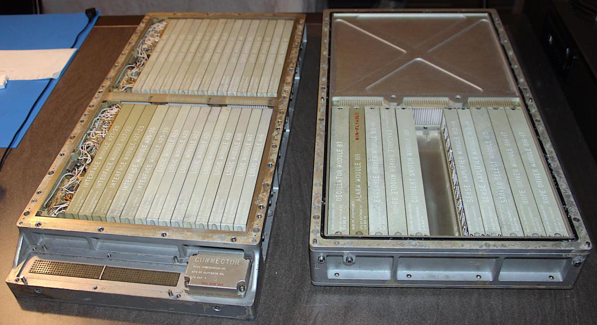
Inside the Apollo Guidance Computer. The power supplies are the tangles of wires on the far left.

Inside the Apollo Guidance Computer. The power supplies are the tangles of wires on the far left.

The photo above shows the Apollo Guidance Computer after separating its two trays. Tray A on the left holds the logic and interface modules, while Tray B on the right has the memory circuitry. The AGC has two power supplies in Tray A on the far left: a +4V power supply and a +14V power supply; the power supplies look like a tangle of wires in the photo. The logic circuitry, entirely built from NOR gates, was powered by 4 volts. The interface circuitry and memory used the 14 volt supply.

The spacecraft generated 28 volts from fuel cells, which combined hydrogen and oxygen to produce both water and electricity.3 The task of the power supplies was to convert the spacecraft's 28 volts into the 4 and 14 volts required by the computer.2 The 4-volt power supply could output about 10 amps (i.e. 40 watts) while the 14-volt power supply could output about 5 amps (i.e. 70 watts).4 Thus, the power supplies are roughly equivalent to laptop chargers (although a laptop charger deals with more challenging AC line voltages).

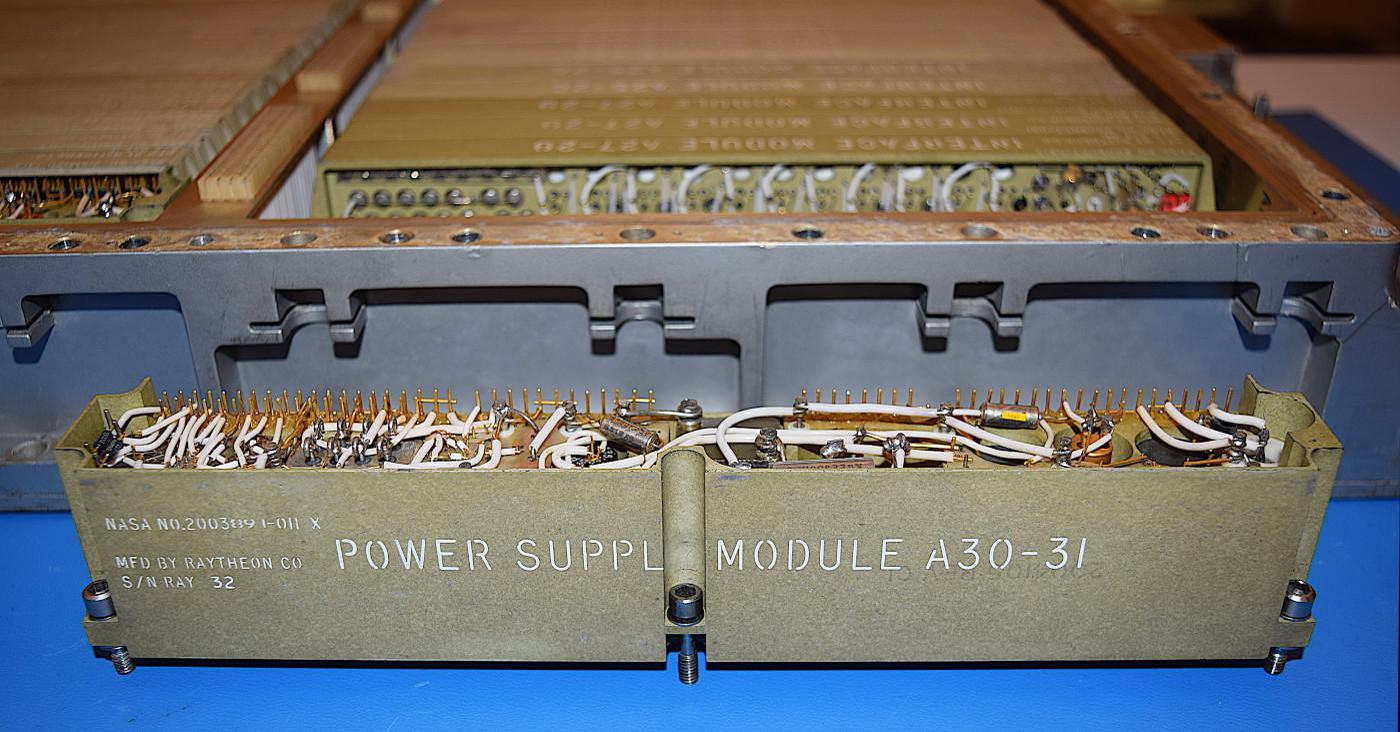
The power supply module in front of the AGC. The module in position A30 provides +14 volts, while the (identical) module in position A31 provides +4 volts.

The power supply module in front of the AGC. The module in position A30 provides +14 volts, while the (identical) module in position A31 provides +4 volts.

Cordwood construction

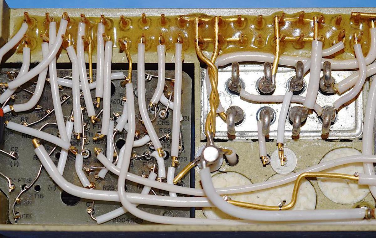
The power supplies, like the AGC's other non-logic modules, were built with cordwood construction. In this high-density technique, cylindrical components were inserted into holes in the module, passing through the module, with their leads exiting on either side.6 The left side of the photo below contains resistors, capacitors, and diodes. Because of the cordwood construction, the components are not visible except for the ends of their leads poking through holes. Point-to-point wiring connected the components with welded connections. (The other side of the module is similar, connecting the other ends of the components.) The shiny rectangle on the right is a relay, used to shut off power for standby operation. The ends of large filter capacitors are visible below the relay.

Cordwood construction in the power supply. On the left, components are mounted vertically through the module, 
with welded wiring on both sides. The metallic box on the right is a relay. Underneath the relay, the ends of filter capacitors are visible.

Cordwood construction in the power supply. On the left, components are mounted vertically through the module, with welded wiring on both sides. The metallic box on the right is a relay. Underneath the relay, the ends of filter capacitors are visible.

Cordwood construction was used for high density in applications from aerospace to Cray's CDC 6600 computer. For flight, the AGC's cordwood wiring was encased (potted) in epoxy, protecting it from vibration.

How the power supplies worked

Because the power supplies needed to be lightweight and efficient, they were switching power supplies, an unusual technology for the time. Most computers back then used linear power supplies, which were simpler but much too inefficient for the AGC since excess voltage is turned into waste heat.5 A switching power supply, on the other hand, switches the input voltage on and off at a high frequency. This yields the desired output voltage with very little wasted energy.

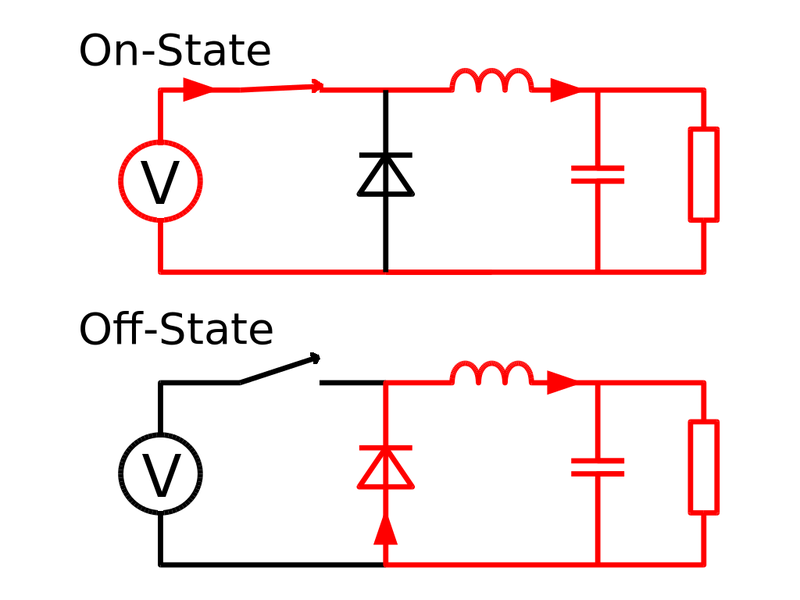
The AGC's power supplies used a common switching circuit called a buck converter, which converts an input voltage to a lower voltage. The diagram below shows the key components: a switch (transistor), inductor, diode, and capacitor. The key idea is that if the switch is closed for more time, more of the input voltage will appear across the load. Thus, the output voltage is controlled by the switch timing. The inductor stores energy and releases it when the switch is open, producing a relatively stable output.

A buck converter rapidly switches between the on state and the off state.
When on, current flows from the voltage source (V) through the switch and inductor to the load (right). When the switch is open, stored energy in the inductor continues to provide current to the load, through the diode. (Source:
Cyril Buttay,
CC BY-SA 2.5).

A buck converter rapidly switches between the on state and the off state. When on, current flows from the voltage source (V) through the switch and inductor to the load (right). When the switch is open, stored energy in the inductor continues to provide current to the load, through the diode. (Source: Cyril Buttay, CC BY-SA 2.5).

A switching power supply requires a complex control mechanism to switch on and off at the right time. The AGC used a technique called PWM (pulse-width modulation), where power is switched on and off at a fixed frequency (e.g. 20 kilohertz), but changing the fraction of the time the power is on to regulate the voltage.

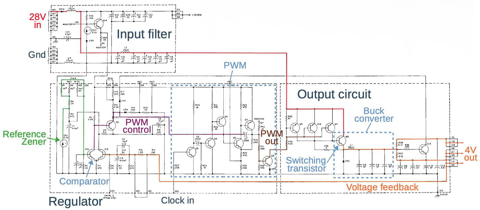
The schematic below shows the AGC's power supply. (Don't worry about reading the details; click for a larger version.) The buck converter itself (outlined in the lower right) has the expected switching transistor, diode, inductor, and capacitors. However, the power supply has many more components to implement the PWM control circuitry.

Schematic of the AGC's power supply. The main signals are highlighted: 28-volt input (red), 4-volt output (orange),
reference voltage (green), comparator output to control the PWM (purple), and PWM output (brown).
(source)

Schematic of the AGC's power supply. The main signals are highlighted: 28-volt input (red), 4-volt output (orange), reference voltage (green), comparator output to control the PWM (purple), and PWM output (brown). (source)

To summarize the power supply's operation, 28 volts (red) is supplied at the upper left and filtered. The buck converter in the output circuit (right) reduces the voltage to 4 volts (orange) On the control side (left), the output voltage is used for feedback. A two-transistor comparator (lower left) compares the output voltage with a reference voltage (green) set by a Zener diode and resistor network. The output of the comparator (purple) goes through the PWM control circuit where it modifies the width of the pulses (brown) produced by the PWM circuit. These pulses drive the switching transistor in the buck converter, closing the feedback loop. The computer's clock signal providing timing for the PWM circuit.7

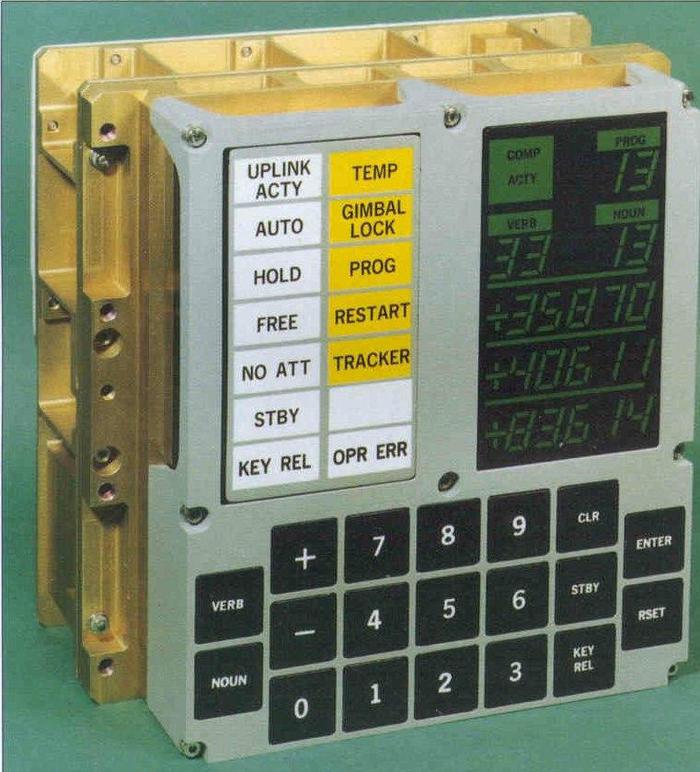
Astronauts interacted with the AGC through the Display/Keyboard (DSKY).
The STBY button (lower right) put the computer in standby mode, which was indicated via the STBY light (left).
Photo from Virtual AGC.

Astronauts interacted with the AGC through the Display/Keyboard (DSKY). The STBY button (lower right) put the computer in standby mode, which was indicated via the STBY light (left). Photo from Virtual AGC.

The power supply also included a standby circuit. By pressing the STBY key on the display/keyboard (DSKY), a relay would disconnect most of the computer's power. This reduced energy consumption when the computer wasn't needed.8

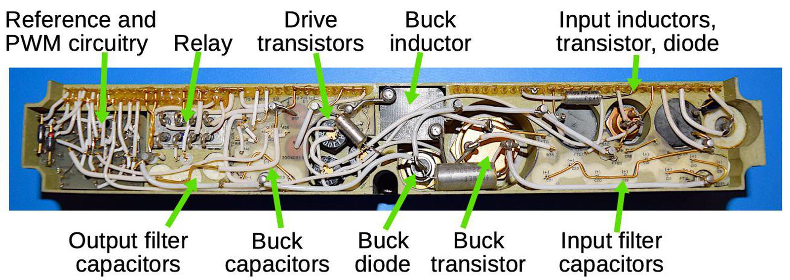
The diagram below shows the top of the power supply module with the major components labeled. Note the large size of the transistors, inductors and filter capacitors compared to the tightly-packed cordwood circuitry on the left. The switching transistor for the buck converter is almost an inch in diameter.

The major components of the AGC's power supply. The components for the buck converter are much larger than the control circuitry.

The major components of the AGC's power supply. The components for the buck converter are much larger than the control circuitry.

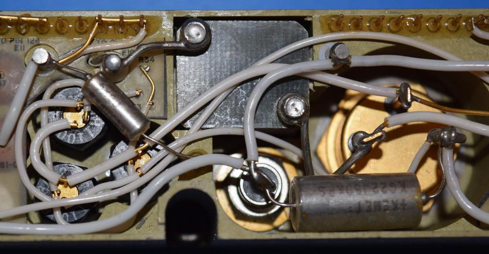
The transistors of the 1960s were barely able to support switching power supplies since they required a power transistor that could operate at both high speed and high current, which was difficult at the time. (Modern transistors (MOSFETs) are cheap and can handle much higher voltages, leading to ubiquitous low-cost phone and laptop chargers that run off an AC outlet.) The switching transistor required a high-current control signal, which was provided by three drive transistors (in a "complementary Darlington" configuration).

Closeup of transistors in the power supply.
The large transistor on the right is the high-current switching transistor.
Driving it required the three transistors on the left.

Closeup of transistors in the power supply. The large transistor on the right is the high-current switching transistor. Driving it required the three transistors on the left.

Testing the power supply

We extensively tested the AGC's components before powering up the system. For the power supply, we first checked all the tantalum capacitors since tantalum capacitors are prone to shorting out. We found that the capacitors were all in good shape with the proper capacitances. This is in contrast to modern capacitors, which often leak or fail after a few years. NASA used expensive aerospace-grade capacitors and X-rayed each one to test for faults, and this made a large difference.

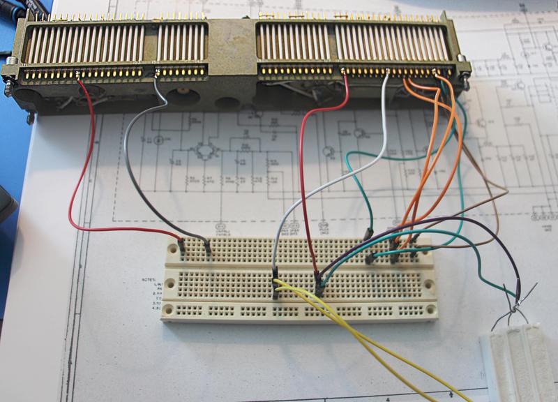
Wiring up each power supply for testing (below) was more complex than you might expect. The AGC used two identical power supplies that supplied 4 or 14 volts. The output voltage was selected by backplane wiring that connected different resistors in the feedback resistor network. We reproduced these connections on a breadboard, as well as connecting up the input and output. Some high-wattage resistors (lower right) served as the load.

The setup we used to test the power supply. Connections were made to the pins on the bottom of the module.
These pins connected the module to the rest of the AGC.
In this view you can see the white wires on the side of the module that connected the circuitry on top of the module to the pins on the bottom.

The setup we used to test the power supply. Connections were made to the pins on the bottom of the module. These pins connected the module to the rest of the AGC. In this view you can see the white wires on the side of the module that connected the circuitry on top of the module to the pins on the bottom.

We powered-up the AGC modules with 28 volts using a current-limited supply to limit potential damage from any faults. We took measurements and found that 4V power supply produced 4.09 volts while the 14V power supply produced 14.02 volts. The quality of the power was good, with about 30mV of ripple. We were somewhat surprised that both power supplies worked flawlessly after 50 years.

Conclusion

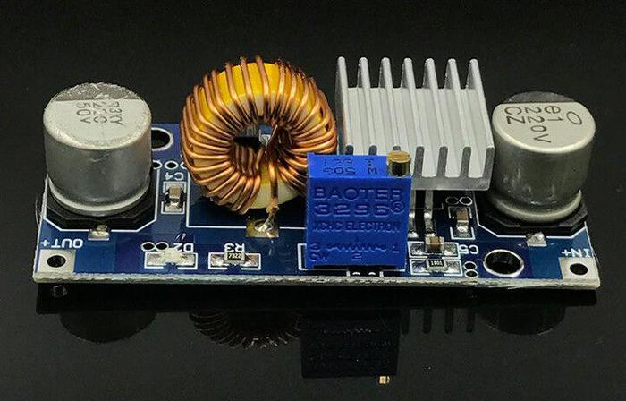
The Apollo Guidance Computer used advanced switching power supplies that were lightweight and efficient. While switching power supplies were exotic in the 1960s, improved semiconductors have made them cheap and ubiquitous. Now the switching transistor, a high-precision voltage reference, and the control logic can be combined on a single chip. The modern equivalent of the AGC's power supply is a tiny 5A buck converter for $1.50 on eBay (below). While I wouldn't trust this converter to get to the moon, let alone still work 50 years from now, it illustrates the dramatic improvements in switching power supply technology. (I've written more about the history of switching power supplies.)

A modern 5A buck converter is compact and costs $1.50.

A modern 5A buck converter is compact and costs $1.50.

To learn more about our AGC restoration, see Marc's series of AGC videos; the video below shows us testing the power supplies. I announce my latest blog posts on Twitter, so follow me @kenshirriff for future articles. I also have an RSS feed. Thanks to Mike Stewart for photos.

Notes and references

  1. The AGC restoration team consists of Mike Stewart (creator of FPGA AGC), Carl Claunch, Marc Verdiell (CuriousMarc on YouTube) and myself. The AGC that we're restoring belongs to a private owner who picked it up at a scrapyard in the 1970s after NASA scrapped it. For simplicity, I refer to the AGC we're restoring as "our AGC". 

  2. The first version of the Apollo Guidance Computer was known as Block I. The AGC was extensively redesigned to produce the Block II version that was flown. The Block I used +3V and +13V power supplies, while the Block II used +4V and +14V. The Block I power supply is documented here in section 4-8.7. The Block II power supply is documented here in section 4-5.9. 

  3. The power systems were different between the command/service module and the lunar module. On the command/service module the 28 volts was fed to the different parts of the spacecraft using two buses (Main A and Main B) for redundancy. Main A bus was connected to the A31 power supply module, while the Main B bus was connected to the A30 power supply module (schematic). The two buses were tied together inside the AGC after passing through power rectifiers, so either bus could power the AGC.

    (You may recall from Apollo 13: "Houston, we've had a problem. We've had a Main B Bus undervolt". When the oxygen tank exploded, the voltage from the fuel cells dropped, triggering the low voltage alarm.)

    The lunar module used batteries for its 28 volt supply, rather than fuel cells. Instead of Main Bus A and Main Bus B, the lunar module had a Commander bus (CDR BUS) and a Lunar Module Pilot bus (LMP BUS). The AGC on the lunar module was only connected to the CDR BUS, so there wasn't redundancy. 

  4. I estimated the wattage of the power supplies by looking at the current-limit feature. The power supplies have two 0.12Ω current-sense resistors. The voltage drop across these resistors will turn on transistor Q13, which will reduce the PWM output and thus the power supply's output voltage. The 4V power supply has the two resistors in parallel (connected by external wiring). Assuming the transistor turns on at 0.6V, this corresponds to a current of 0.6V / 0.06Ω = 10 A. The 14V power supply uses one current-sense resistor, so it will be limited to around 0.6V / 0.12Ω = 5A. 

  5. Some calculations show the problem with using a linear power supply. The AGC's power supply produced 4 volts at 10 amps, which is 40 watts. A linear power supply would dissipate 24 volts (of the 28 volts) at 10 amps, i.e. 240 watts. The linear power supply would be 14% efficient, wasting 86% of the energy. When you need tanks of liquid hydrogen and oxygen to provide the energy, wasting 86% is unacceptable. In addition, disposing of waste heat on a spacecraft is difficult, so an additional 240 watts would be a problem. 

  6. In the power supplies, the cordwood components are mounted differently from the other cordwood modules. Most AGC modules had components running from one side to the other as shown below, while components in the power supply went from top to bottom, parallel to the pins. This allowed the use of longer components, in particular, the large filter capacitors.

    Most of the cordwood modules, such as this interface module, had components running from side-to-side through the module.

    Most of the cordwood modules, such as this interface module, had components running from side-to-side through the module.

  7. One interesting thing about the power supply is that the PWM circuit was driven by the computer's oscillator. But the oscillator was powered by the power supply, raising a chicken-and-egg problem of how the system started up. The solution was that the PWM circuit would self-oscillate at 20 kilohertz if there was no external clock signal, so it would still produce the correct output voltage. Once it provided power to the oscillator module and the oscillator produced a clock signal, the power supply synchronized to this clock signal (50 kilohertz for the 4V supply and 100 kilohertz for the 14V supply). 

  8. The standby (STBY) key on the DSKY was changed to PRO (proceed) on later versions of the DSKY and the functionality was changed somewhat. 

Looking inside a 1970s PROM chip that stores data in microscopic fuses

The MMI 5300 was a memory chip from the early 1970s, storing 1024 bits in tiny fuses.1 Unlike regular RAM chips, this was a PROM (Programmable Read-Only Memory); you programmed it once by blowing fuses and then it held that data permanently. The chip I examined originally cost $70 and was built by MMI (Monolithic Memories Incorporated), a leading PROM manufacturer at the time.

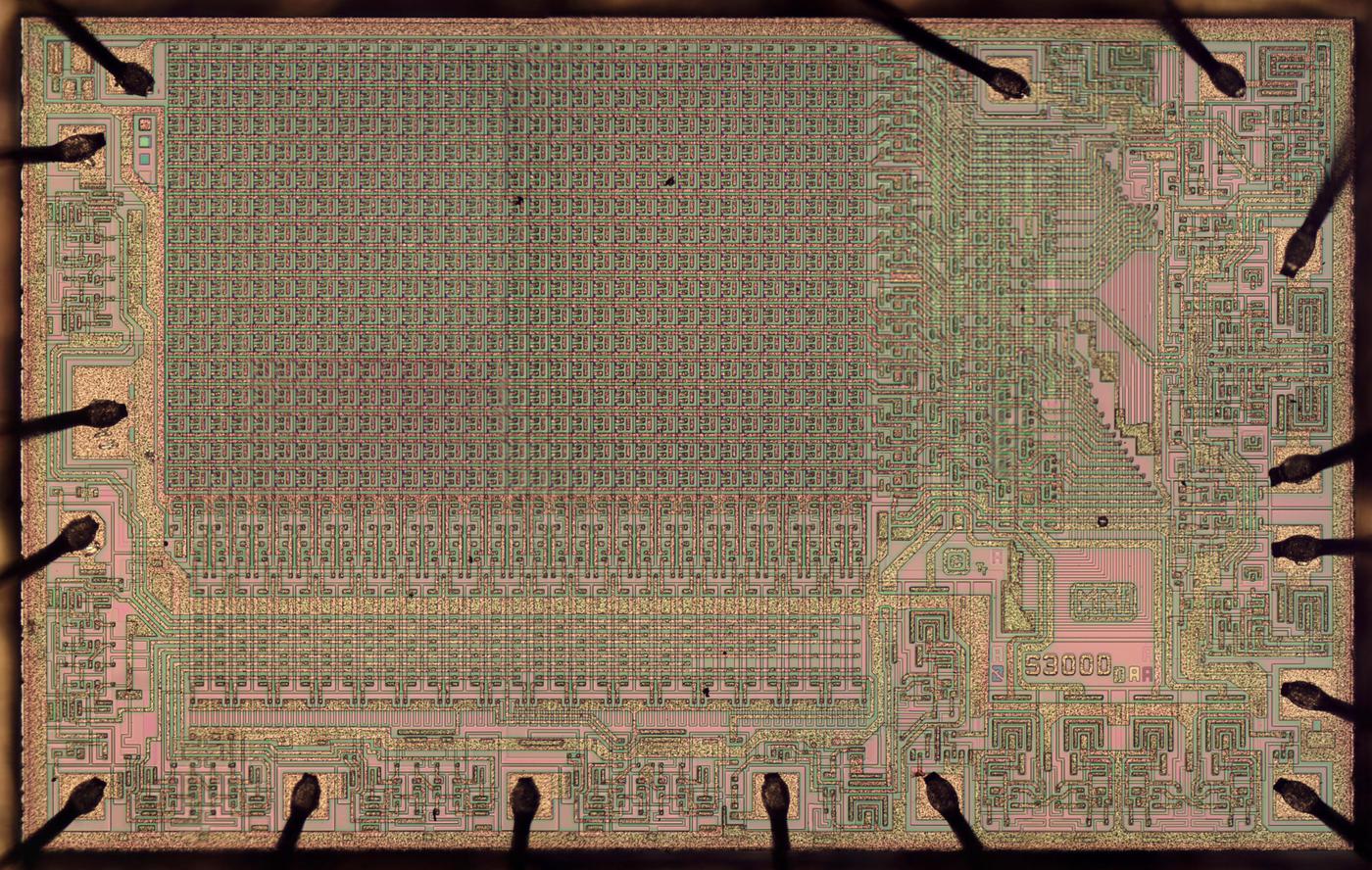
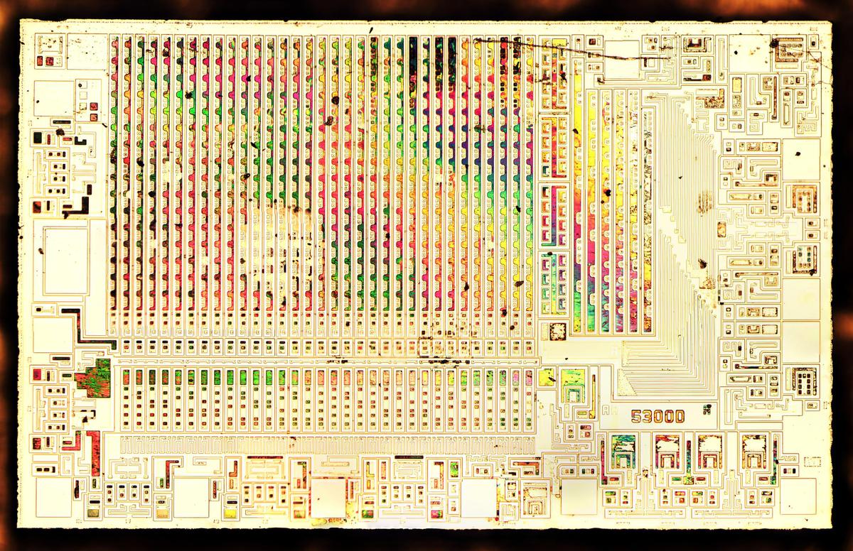
The highly magnified photo below shows the chip's silicon die. The metal layer on top of the silicon is most visible in this photo; the transistors and resistors fabricated from silicon are underneath. The wires around the edges are the 16 bond wires between the silicon die and the external pins. In the upper left, the 1024 bits of data are stored in a 33×33 array of diodes and fuses. (I'll explain the extra row and column below.) This chip is built from NPN transistors, unlike the MOS transistors used in most modern chips.

Die of the MMI 5300 PROM chip, holding 1024 bits of information. Click image for a larger version.

Die of the MMI 5300 PROM chip, holding 1024 bits of information. Click image for a larger version.

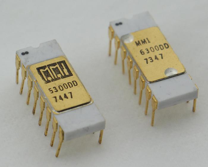
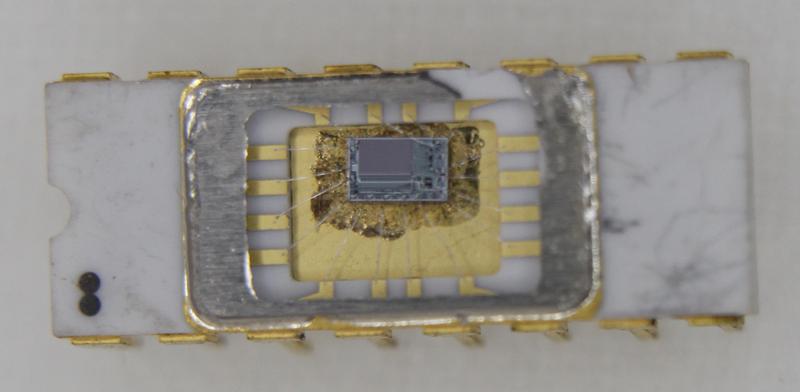
To produce the die photo, I started with the chips below, in their 16-pin ceramic packages; the 5300 and 6300 chips are essentially the same.2 Since the chips were in ceramic packages, I could decap the chip simply by knocking the metal lid off with a chisel, revealing the silicon die.

The MMI 5300 and 6300 PROM chips are in ceramic packages. The chips have 1974 and 1973 date codes.

The MMI 5300 and 6300 PROM chips are in ceramic packages. The chips have 1974 and 1973 date codes.

In the photo below, the silicon die is mounted very off-center in the package. It's unclear if that is intentional or sloppy manufacturing. Tiny bond wires connect the die to the metal contacts of the package.

The MMI 5300 PROM with the lid removed, exposing the die.

The MMI 5300 PROM with the lid removed, exposing the die.

Inside the chip

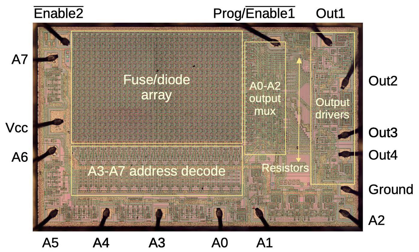
The diagram below shows the main parts of the chip, with the pins labeled. The chip stores 1024 bits as 256 4-bit words. The 8 address lines A0-A7 select one of the 256 words, and the bits are output on pins Out1-Out4. The Program pin is used to store data in the chip by blowing fuses. The Vcc and ground pins power the chip.

Die of the 5300 PROM with components labeled.

Die of the 5300 PROM with components labeled.

The 1024 bits of data are stored in a 33×33 array of diodes and fuses. Note that the data array only takes up about a quarter of the chip; the rest of the chip holds the supporting circuitry. Below the data array, address decode circuitry used the address lines to select one of 32 columns in the array. To the right, DTL multiplexers4 reduced the 32 rows of output to the 4 desired outputs. The output drivers amplified these signals and sent them to the output pins.

The fuses

The chip stored data in tiny fuses. An intact fuse represented a 1, while a blown fuse represented a 0. Thus, the chip was shipped containing all 1's, and the user programmed the chip by blowing fuses where a 0 bit was required. The fuses were fabricated from tiny regions of Nichrome metal that heat up and melt under high voltage. (Nichrome is a nickel-chromium alloy that has much higher resistance than typical metals, causing it to heat up. It is commonly used in applications such as toasters.)

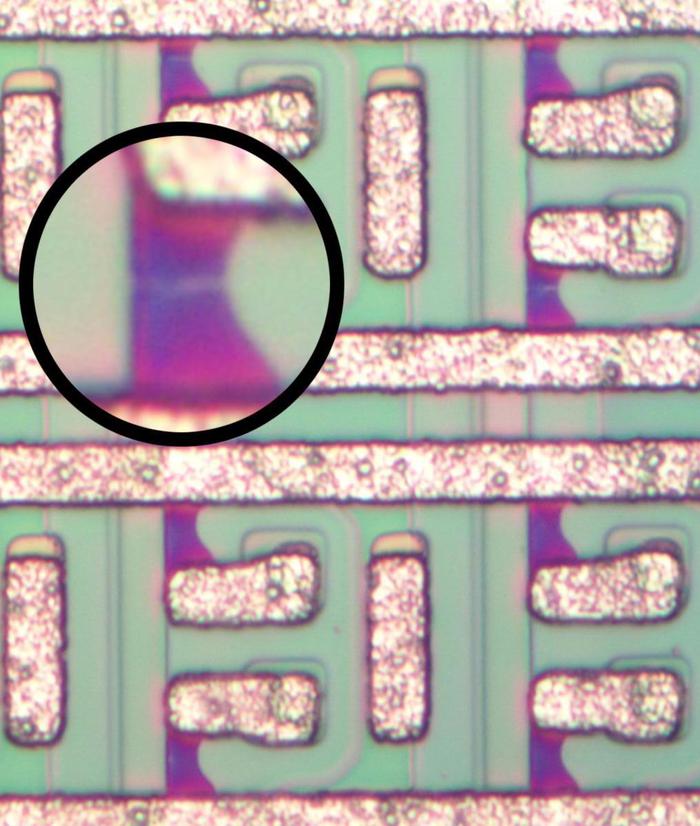
A closeup of the fuses (purple) that store data. Inset circle shows a magnified fuse, showing the tiny horizontal crack indicating the fuse was blown.

A closeup of the fuses (purple) that store data. Inset circle shows a magnified fuse, showing the tiny horizontal crack indicating the fuse was blown.

The fuses are visible in the die photo above; they are the purple regions between the metal wiring. The fuses are very small, about 8µm long. I expected a blown fuse would vaporize entirely, but instead a blown fuse contains a tiny crack roughly 700 nm wide. (This is the wavelength of red light, so the crack is just barely visible under the microscope.)

Address decoding

The PROM stored 1024 bits as 256 words of 4 bits. However, the bits are physically arranged in a 33×33 grid since a square memory grid is more efficient than a highly-rectangular one. To access the memory, address bits A3-A7 select one of the 32 columns. The selected 32 bits in the column go through the multiplexers at the right, which select one bit out of each group of eight, based on address bits A0-A2. The four selected bits become the four outputs. Thus, addressing has two parts—one to select the column and one to select the four output bits—and they have separate circuitry,

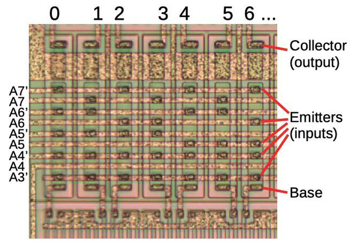
Column selection uses 32 NAND gates, implemented with multiple-emitter transistors.3 (The N and P silicon regions of the transistors are visible as rectangular boxes, with the brownish metal layer on top connecting the regions together.) Each NAND gate has a different combination of address bits A3-A7 either inverted or uninverted, so each address activates a different NAND gate, selecting the associated column. You can see the binary counting in the emitters. The A7' and A7 lines alternate connections every column. The A6'/A6 connections alternate every two columns, while A5'/A5 alternate every four, and so on.

Part of the column address decoder. Each (vertical) transistor decoded a particular address, determined by which address lines are connected to the emitters. There were 32 columns in total.

Part of the column address decoder. Each (vertical) transistor decoded a particular address, determined by which address lines are connected to the emitters. There were 32 columns in total.

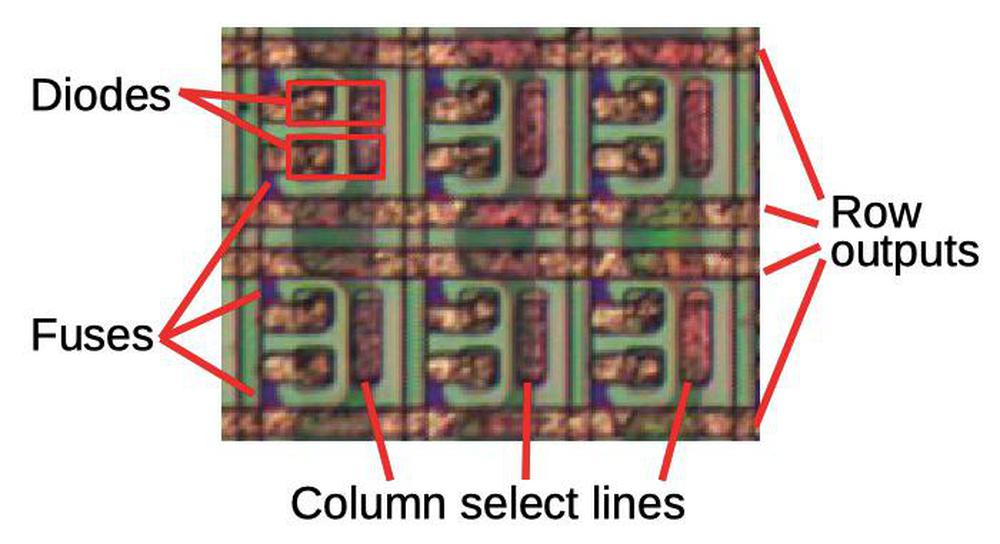
The data array consists of a diode and fuse for each bit. (Without diodes, the bits would all be shorted together.) If the fuse is present, a low signal on the selected column will pull the corresponding row low through the diode (indicating a 1). If the fuse is blown, the row will remain high (indicating a 0). Thus, by blowing fuses, bits are programmed into the memory array. The diodes themselves are mostly hidden under the metal layer below. The column select lines run vertically in the silicon under the metal layer; the metal stripes on top reduce the resistance.

12 bits in the memory array. Each bit has a diode and fuse between a column select line and a row line.

12 bits in the memory array. Each bit has a diode and fuse between a column select line and a row line.

Programming

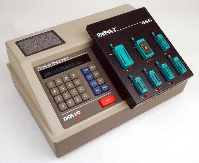
To program the PROM, the user melted the necessary fuses one at a time using carefully-controlled high voltage pulses. After selecting the desired address, 27 volts was applied to the programming pin (a much higher voltage than the typical 5V TTL level). After a carefully-timed interval, the desired output was brought to 20 volts for a few microseconds to blow the fuse. (The timing and voltages needed to be precise so the fuse would blow without damaging other parts of the chip.) The process was repeated for each desired 0 bit. Customers used a PROM programmer such as shown below to perform these operations automatically.

The Data I/O PROM programmer. It had sockets of various sizes (turquoise) to hold different sizes of chips. This programmer cost about $6000. Photo: Michael Holley.

The Data I/O PROM programmer. It had sockets of various sizes (turquoise) to hold different sizes of chips. This programmer cost about $6000. Photo: Michael Holley.

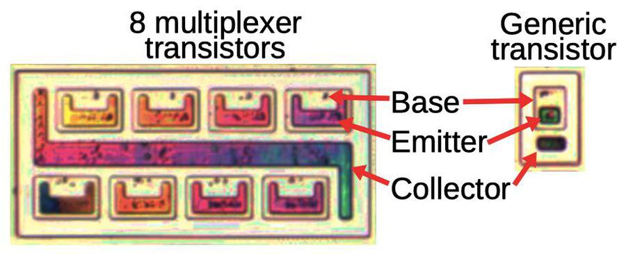
For the most part, reading a fuse and blowing a fuse used the same circuitry; the difference was the output pin circuit, which could either output a bit or sink a large current to blow the fuse, depending on the programming mode.5 The transistors along the programming path were larger than regular transistors to handle the larger current. For example, the diagram below compares the multiplexer NPN transistors to a typical NPN transistor on the chip. Also note that the 8 transistors in a multiplexer share a single collector (the multiplexer output).

Eight transistors in a multiplexer (left) compared to a typical NPN transistor (right). The metal layer was removed for this photo. The remaining oxide gives the transistors a colored appearance. N-doped silicon appears darker.

Eight transistors in a multiplexer (left) compared to a typical NPN transistor (right). The metal layer was removed for this photo. The remaining oxide gives the transistors a colored appearance. N-doped silicon appears darker.

Testing

Before examining this chip, I didn't consider how difficult it was for the manufacturer to test a PROM. Most chips can be extensively tested before shipping to the customer, but you can't test the PROM fuses without irreversibly programming the chip. Even testing the address decode logic is difficult; since the chip is manufactured with all 1's, you'd read the same result even if the address circuitry is broken.

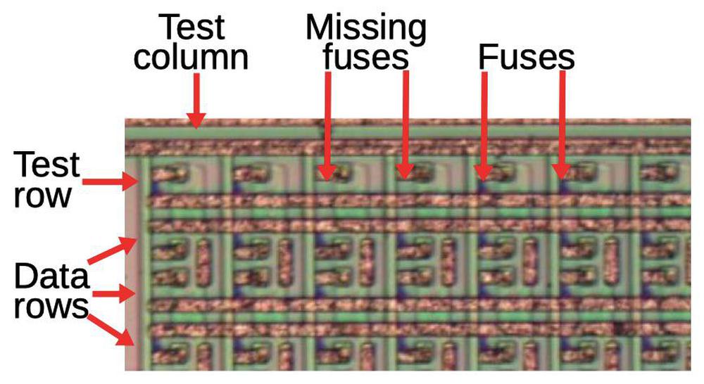
The chip included an extra row and column of fuses for testing.

The chip included an extra row and column of fuses for testing.

To support testing, the chip contains an extra row and column of fuses.6 As a result, the storage grid was 33×33, rather than the 32×32 grid you'd expect. Half of the test fuses were missing, so reading the correct pattern of 0's and 1's tested the address decoders. By blowing test fuses and reading the results, the programming characteristics could be tested. The datasheet says that the chips should have a programming yield of over 95%. Compared to most integrated circuits, this is a high failure rate, but it's understandable given the difficulties of testing the chip.

Unused circuitry

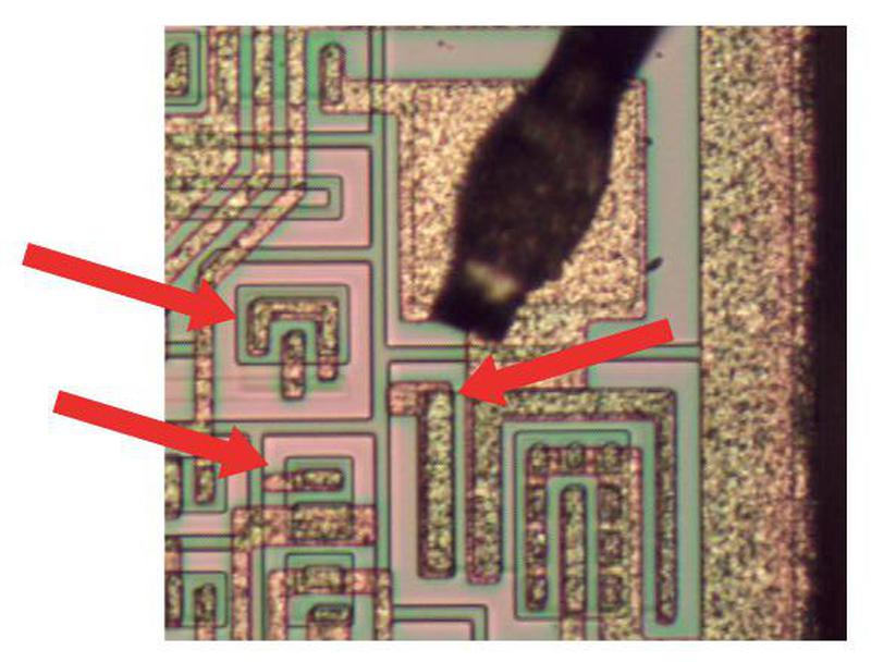
One interesting feature of the 5300 die is that it has some transistors that aren't connected to anything else in the chip. The diagram below shows some of the unused transistors in the output circuitry. There are no metal connections from these transistors to the rest of the chip, making them apparently useless.

The output driver circuitry has some unused transistors, marked with arrows.

The output driver circuitry has some unused transistors, marked with arrows.

The reason for these unused transistors is that the same silicon layout could be used for slightly different PROM chips, depending on how the metal layer was wired up. The 5300 PROM had open-collector outputs, but a tri-state version (6301) was also available.7 Both chips used the same silicon die, but had small modifications to the metal layer to wire the transistors differently. Since the 5300 didn't need output transistors to pull the output to 1, these were left unconnected, yielding the unused circuitry seen above.

Conclusion

PROM chips were an important part of early computer systems, often holding the boot code, but their popularity peaked in the early 1980s as they were replaced by erasable PROM (EPROM) chips. EPROM chips had a distinctive quartz window over the die; shining ultraviolet light on the chip erased it, so it could be reused. EPROMs in turn were replaced by electrically-erasable PROMs (EEPROMs), similar to flash memory. To see how much technology has improved, consider that the 6300 PROM chip cost $70 in 1971 and stored 128 bytes. Now you can get a 128 GB flash drive for under $20: a billion times the storage, plus you can write it more than once.

Die with the metal stripped off to expose the silicon. This makes the structure of the transistors visible. The thin remaining oxide layer produces a rainbow effect in some areas.

Die with the metal stripped off to expose the silicon. This makes the structure of the transistors visible. The thin remaining oxide layer produces a rainbow effect in some areas.

I announce my latest blog posts on Twitter, so follow me @kenshirriff for future articles. I also have an RSS feed. Thanks to Marc Verdiell for supplying the chip.

Notes and references

  1. For more information on the chip, see the MMI Bipolar LSI Databook chapter 2. 

  2. The 6300 was the commercial 1K PROM, while the 5300 was the same chip specified for the military temperature range (-55 °C to +125 °C). The 6200/5200 was a compatible ROM chip, so you could design your system using the 6300 PROM and then drop in a mask-programmed ROM when everything was working. (A mask-programmed ROM was cheaper, but needed to be manufactured in large quantities.) 

  3. Multiple-emitter transistors may seem strange, but they are used in the common 7400-series TTL chips. 

  4. I suspect that diode-transistor logic was used instead of TTL for the output multiplexer because the simpler DTL circuit worked better with the high programming voltages. The DTL circuitry uses very large resistors biased to the programming voltage. They are visible near the right side of the die. 

  5. The current path for reading and programming bits is as follows. When reading a bit, the output driver circuit was pulled to ground through a multiplexer transistor, the (intact) fuse, the associated diode, and finally the column select transistor. To blow a fuse, the programming pulse disabled the output driver circuits and transistors connected the output pins directly to the multiplexers. Then the high voltage pulse on the output pin followed the same path as before (multiplexer transistor, fuse, diode, column select transistor and ground), but the much higher current blew the fuse, permanently switching the bit to 0. 

  6. One interesting question is how the test fuses are accessed. There are no test points on the chip; from the circuitry it appears that these fuses are accessed by applying unusual voltages to some of the pins. To access the row of test fuses at the top of the chip, the programming pin is raised to a higher voltage. To read or write the column of test fuses at the left of the chip, address pin A6 is pulled higher. This allows the row select logic, output drivers and programming circuitry to be tested. (These actions are undocumented and based on my reverse engineering.) 

  7. The motivation for using tri-state or open-collector outputs is that often multiple memory chips were connected together to create a larger memory. The problem was how to combine the outputs. One solution was "open collector" outputs: essentially an output is either 0 or "nothing", and an external resistor pulls the output to 1 if it's not 0. A second solution was tri-state outputs: an output can be 0, 1, or "nothing" if not enabled. Since only one output was enabled at a time, the outputs could be tied together. 

Apollo Guidance Computer: Dipstiks and reverse engineering the core rope simulator

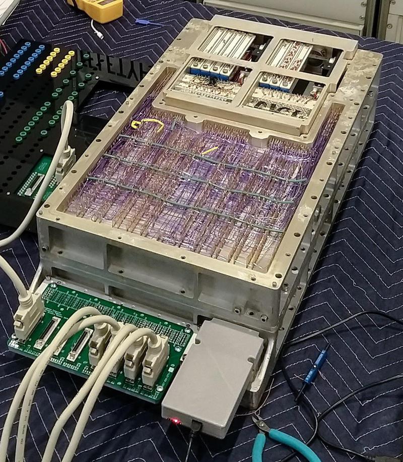
Onboard the Apollo spacecraft, the revolutionary Apollo Guidance Computer helped navigate to the Moon and land on its surface. The AGC's software was physically woven into permanent storage called core rope memory. We1 are restoring an Apollo Guidance Computer (below), which is missing the core ropes, but instead has core rope simulator boxes. These boxes were used during development and ground testing to avoid constantly manufacturing ropes. The core rope simulator is undocumented, so I reverse-engineered it, built an interface, and we used the simulator to run programs on our Apollo Guidance Computer. But we ran into some complications along the way.

The Apollo Guidance Computer with the cover removed, showing the wire-wrapped backplane. At the back, rope simulator boxes are visible in the core rope slots. The interface boards at the front are modern.

The Apollo Guidance Computer with the cover removed, showing the wire-wrapped backplane. At the back, rope simulator boxes are visible in the core rope slots. The interface boards at the front are modern.

The AGC's core ropes

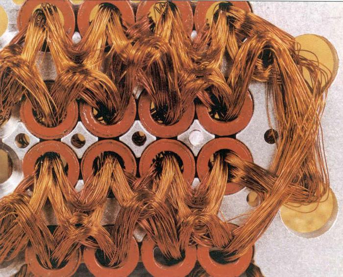
The Apollo Guidance Computer held six core rope modules, each storing just 6 kilowords of program information (about 12 kilobytes).2 Core rope modules were a bit like a video game ROM cartridge, holding software in a permanent yet removable format. Programs were hard-wired into core rope by weaving wires through magnetic cores. A wire passed through a core for a 1 bit, while a wire going around a core was a 0 bit. By weaving 192 wires through or around each core, each core stored 192 bits, achieving much higher density than read/write core memory that held 1 bit per core.

Detail of core rope memory wiring from an early (Block I) Apollo Guidance Computer. Photo from Raytheon.

Detail of core rope memory wiring from an early (Block I) Apollo Guidance Computer. Photo from Raytheon.

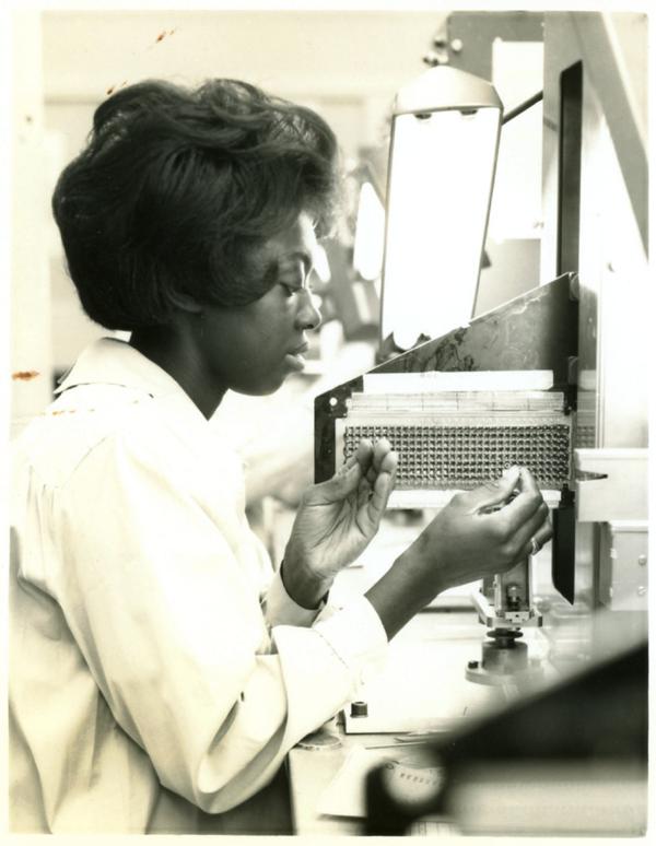
Manufacturing a core rope was a tedious process that took about 8 weeks and cost $15,000 per module. Skilled women wove the rope by hand, threading a hollow wire-filled needle back and forth through the cores, as shown below3. They had the assistance of an automated system that read the program from a punched tape and positioned an aperture over the matrix of cores. The weaver threaded the needle through the aperture to install the wire in the right location. Once completed, the core rope was mounted in a module along with hundreds of resistors and diodes and encased in epoxy to make it solid for flight. (See my earlier article on core rope for details.)

A woman weaving a core rope memory, wiring software into read-only memory.

A woman weaving a core rope memory, wiring software into read-only memory.

The core rope simulator

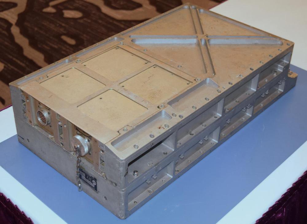
Since weaving a core rope was a time-consuming and expensive process, an alternative was required during development and ground testing. In place of the core ropes, NASA used rope simulators4 that allowed the AGC to load data from an external system. Our Apollo Guidance Computer was used for ground testing so it didn't have core ropes but instead had a core rope simulator. The simulator consists of two boxes that plugged into the AGC's core rope slots, each box filling three rope slots. These boxes are visible in the upper-left side of the AGC below, with round military-style connectors for connection to the external computer.

The core rope simulators are installed in the left side of the AGC in place of the real core ropes. Two round connectors on the left allowed the simulators to be connected to an external computer that provided the data.

The core rope simulators are installed in the left side of the AGC in place of the real core ropes. Two round connectors on the left allowed the simulators to be connected to an external computer that provided the data.

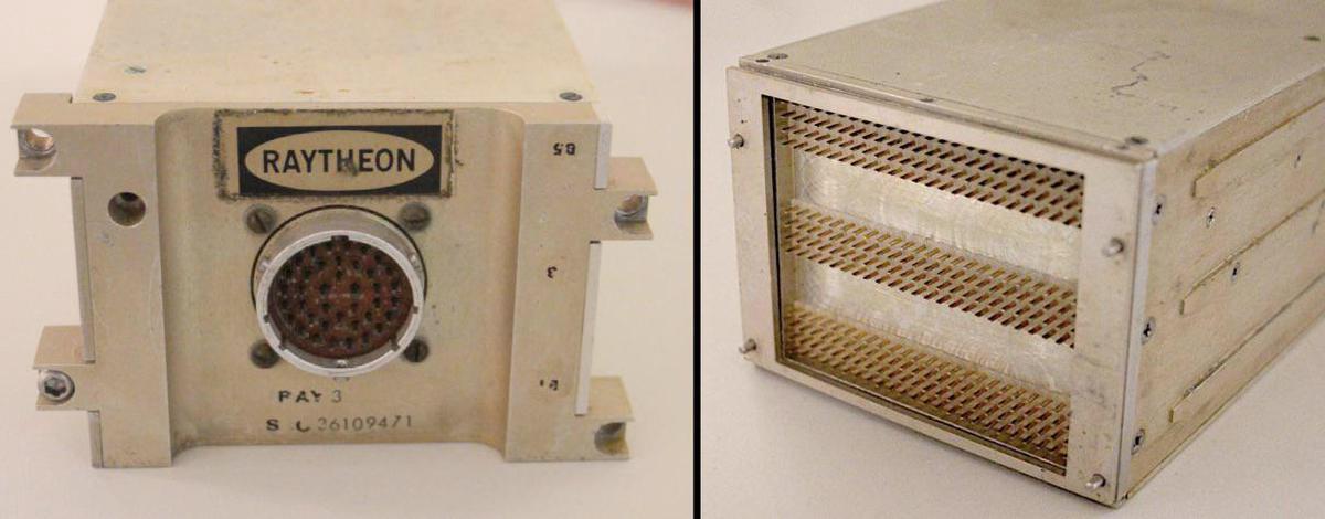
Although we have extensive documentation for the Apollo Guidance Computer, I couldn't find any documentation on the simulator boxes. Thus, I had to reverse engineer the boxes by tracing out all the circuitry and then figuring out what the boxes were doing. From the outside, the boxes didn't reveal much. One end of each box has a round MIL-Spec plug for connection to an external system. The other end has three groups of 96 pins that plugged into the AGC. Each group of pins took the place of one core rope module.

Each core rope box communicated with the external system via a round 39-pin connector.
Each box had three sets of 96 pins that plugged into the AGC, replacing three rope modules.

Each core rope box communicated with the external system via a round 39-pin connector. Each box had three sets of 96 pins that plugged into the AGC, replacing three rope modules.

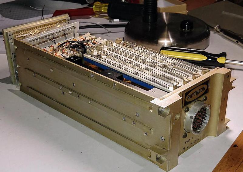
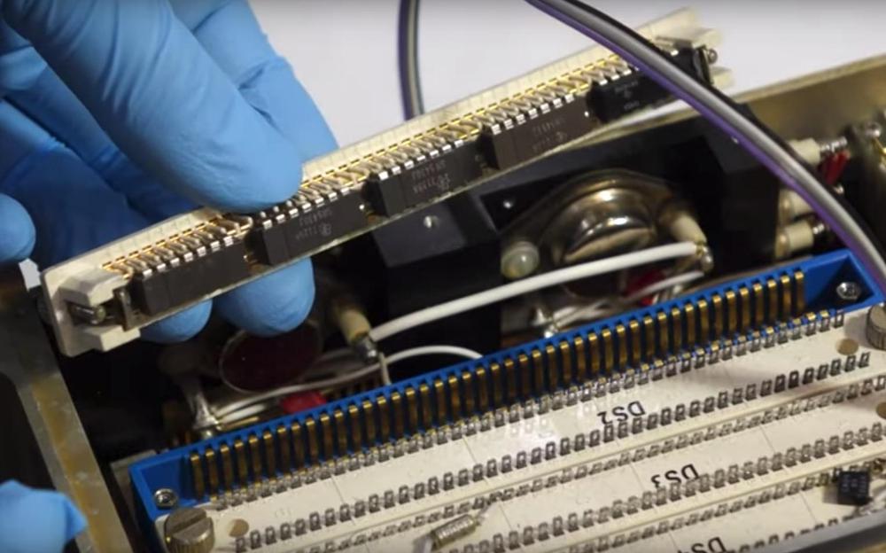
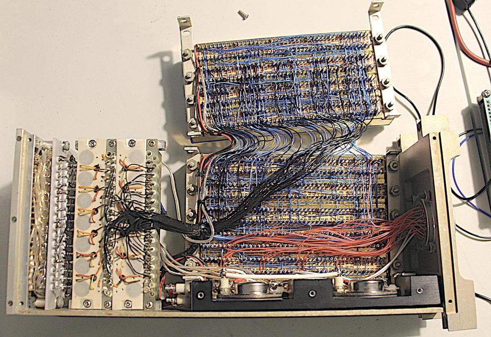
Opening up the boxes showed their unusual construction techniques. Part of the circuitry used high-density cordwood construction which mounted components vertically through holes in a metal block. On either side of the block, the component leads were welded to point-to-point wiring. Other circuitry in the boxes used standard integrated circuits (7400-series TTL). But unlike modern printed circuit boards, the chips were mounted inside plastic units called Dipstiks and wire-wrapped together.

A rope simulator box, partially disassembled. The round external connector is visible at the right, and the pins to connect to the AGC at the left. Analog circuitry with cordwood construction is center-left. To the right, several Dipstik modules are visible, white with rows of pins.

A rope simulator box, partially disassembled. The round external connector is visible at the right, and the pins to connect to the AGC at the left. Analog circuitry with cordwood construction is center-left. To the right, several Dipstik modules are visible, white with rows of pins.

Cordwood construction

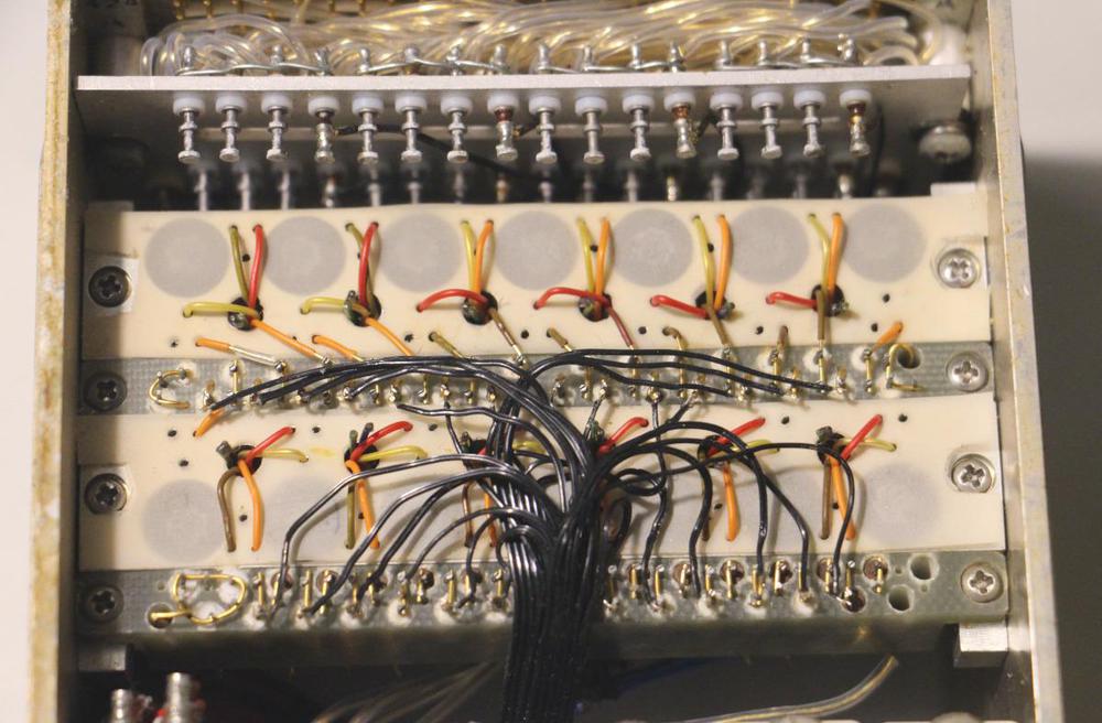
Cordwood construction was extensively used in the Apollo Guidance Computer for analog circuitry, and the cordwood construction in the rope simulators is similar (below). The white circles in the center are the ends of resistors and diodes mounted vertically through the module, with connections welded on either side. These components are stacked together densely, like wood logs, giving cordwood construction its name. Pulse transformers are under the large gray circles. Similar pulse transformers are on the other side of the module with their orange, yellow, red, and brown wires emerging from the holes. The black wires connect the cordwood circuitry to the digital logic. At the top of the photo, the posts have diodes and resistors mounted behind them, along with connections to the pins that plug into the AGC.

A closeup of the cordwood circuitry in a rope simulator box.

A closeup of the cordwood circuitry in a rope simulator box.

The main purpose of the cordwood circuitry was to provide electrical isolation between the Apollo Guidance Computer's circuitry and the rope simulator boxes. In modern circuitry, this function would be implemented with optoisolators but the rope simulator used small pulse transformers instead. Because each box receives signals directed to three different rope modules, numerous diodes merge the three signals into one. Resistors control the current through the pulse transformers.

Reverse-engineering the analog cordwood circuitry was a pain. First, none of the components were visible since they are embedded in the module. I had to use a multimeter to try to figure out what the components were. Second, since cordwood construction has connections on both sides, I spent a lot of time flipping the box back and forth to find the connection I wanted. Finally, I couldn't come up with a good way of drawing a diagram of cordwood construction without ending up in a maze of lines.

Digital logic and the Dipstiks

The Dipstik was a plug-in module introduced in 1968 to simplify prototyping with integrated circuits. It replaced printed circuit boards with a packaging system that provided twice the density. (See this vintage Dipstik ad.) The idea of the Dipstik was a plastic connector block with wire-wrap pins on the bottom for wiring up the circuit. The integrated circuits were clipped into a carrier that fit into the connector block. The carrier had solder lugs on top for additional components, such as decoupling capacitors. (The photo below shows Dipstik modules with one IC carrier removed. Each carrier held 5 integrated circuits.) The pins of the integrated circuit were sandwiched between contacts on the carrier and contacts on the connector block. It seemed like a great idea but turned out to be unreliable. As the plastic flexed and bowed out, the contacts with the pins became unreliable. (This was a problem both for contemporary Dipstik users and for us decades later.) The Dipstik was a stock market failure.

A Dipstik package opened up. The carrier (left) holds the ICs, and is inserted into the connector block (right). Photo courtesy of Marc Verdiell.

A Dipstik package opened up. The carrier (left) holds the ICs, and is inserted into the connector block (right). Photo courtesy of Marc Verdiell.

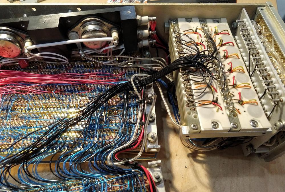
The photo below shows the wire-wrapped connections on the underside of the Dipstiks. Tracing this was extremely tedious since I couldn't follow a wire through the sea of identical blue wires. Instead, I had to beep everything out with a multimeter to find what was connected to what. Then I could construct a schematic diagram of the logic circuitry and ponder what it was doing.5 In total, the rope simulator used about 50 ICs.

Each rope simulator box contains complex circuitry. On the left, wire-wrapped wiring connects the TTL integrated circuits. On the left, the analog components are mounted using cordwood construction. At the back, two voltage regulators in large metal TO-3 packages are mounted on a heat sink.

Each rope simulator box contains complex circuitry. On the left, wire-wrapped wiring connects the TTL integrated circuits. On the left, the analog components are mounted using cordwood construction. At the back, two voltage regulators in large metal TO-3 packages are mounted on a heat sink.

Based on the dates on the components, the simulator boxes were built in 1971. Even though this is just a few years after the design of the AGC, the technology in the simulator boxes is much more advanced, illustrating the rapid changes in IC design between the mid-1960s and the early 1970s. The AGC was built with simple integrated circuits, each containing two NOR gates and built with primitive resistor-transistor logic (RTL). The simulator boxes, on the other hand, were built from more complex 7400-series chips6 containing up to a dozen TTL (transistor-transistor logic) gates. Unlike the obsolete flat-pack integrated circuits in the AGC, the simulator boxes used DIP (dual in-line package) ICs, a packaging style that is still in use.

Results of reverse engineering

After tracing out all the circuitry, I figured out how the rope simulator worked and created a schematic.

Essentially, one box decodes the address being accessed, while the second box sends the desired data to the AGC. (I'll call these the "address box" and "data box".)7

The address box takes the rope signals and converts them into a binary address. This task is not straightforward because the signals it receives are 14-volt high-current pulses designed to flip the rope cores. These pulses are also separated in time since some flip the core and others flip the core back. Finally, the pulses sent to the ropes are not a simple address, but also signals to select one of the 6 rope modules, signals to select one of 12 strands in a module.

The address box uses pulse transformers to convert the 14-volt pulses into TTL signals. It has a bunch of AND-OR logic to convert the signals into a binary address. (This is not trivial because each module holds 6 kilowords, not a power of 2, so a lot of bit manipulation is required.) A flip flop latches the address when it is available. Finally, resistor-capacitor one-shots control the timing, determining from the various signals when the address is ready and when the result should be sent to the AGC.

The data box is simpler. It receives 16 bits of data from the external system and sends signals to the AGC's sense amplifiers simulating the millivolt output from a core. These signals are generated via pulse transformers. The address box and data box communicate with each other via wires on the AGC backplane.

The boxes communicate with the external system via differential signals, to avoid picking up noise on long cables. The boxes contain LM109 5-volt regulators to power their TTL circuits. One box receives unregulated DC through the external connector, and sends unregulated DC to the other box through the AGC's backplane wiring. (This seems strange to me.)

With the address box opened, the wire-wrapped circuitry is visible.

With the address box opened, the wire-wrapped circuitry is visible.

The BeagleBone interface

Once I had reverse-engineered the core rope simulator, the next step was to build an interface that could provide program data to the simulator. I used a BeagleBone, a tiny single-board Linux system. The advantage of the BeagleBone is that it includes fast microcontrollers that could respond to the AGC's memory requests quickly, in real time. (I've written about the BeagleBone's PRU microcontrollers before, and used them to make a Xerox Alto Ethernet interface.)

The interface to the rope simulator consists of a board plugged into a BeagleBone. The two cables from the interface board go to the two simulator boxes.

The interface to the rope simulator consists of a board plugged into a BeagleBone. The two cables from the interface board go to the two simulator boxes.

I designed an interface board that plugged into the BeagleBone. The board is pretty straightforward: some AM26C32 differential line receivers to convert the differential signals from the simulator into 3.3V logic signals for the BeagleBone, and some AM26C31 differential line drivers to send signals to the simulator.8 I designed the board in KiCad and PCBWay manufactured it. They are a sponsor of our AGC restoration, so send them some business :-)

I wrote some software that runs on the PRU, the BeagleBone's microcontroller. This software is basically a state machine that waits for an address from the simulator box, waits for the timing signal, reads the word from BeagleBone RAM, and sends the word to the simulator box. The software is on Github.

Problems with the core rope simulator

The core rope simulator boxes were not built to the standard of the Apollo Guidance Computer, and I ended up spending a lot of time debugging them.10 Many welds in the cordwood circuitry were broken and needed to be soldered. (I don't know if the welds went bad over time or if we broke connections while reverse engineering.) We also found a short circuit on a Dipstik and a bad IC.

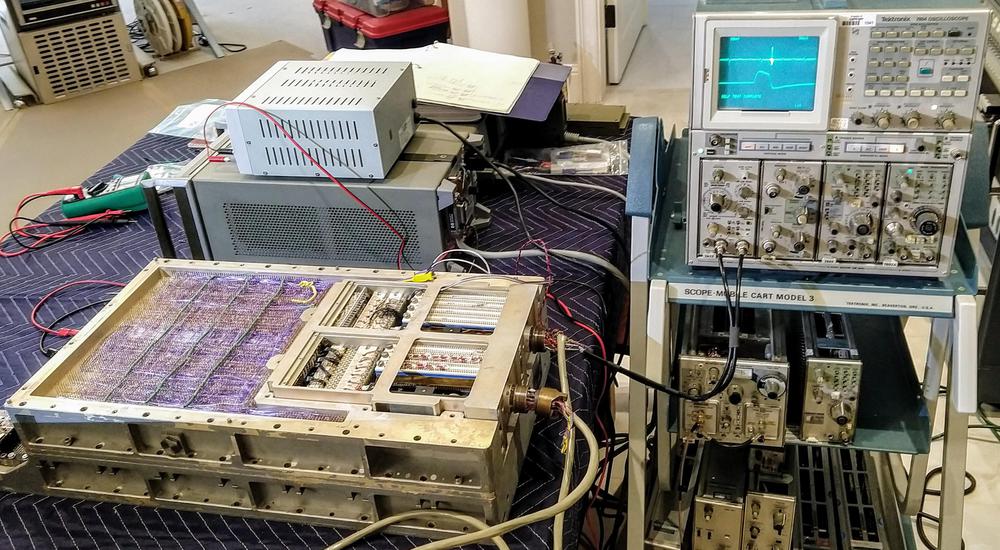
Debugging the simulator boxes. We're used Marc's vintage Tektronix 7854 scope (1980) to examine the pulse transformer's differential signals. The problem turned out to be a broken connection in the cordwood circuitry. Behind the AGC are the power supplies for the AGC and the rope simulator.

Debugging the simulator boxes. We're used Marc's vintage Tektronix 7854 scope (1980) to examine the pulse transformer's differential signals. The problem turned out to be a broken connection in the cordwood circuitry. Behind the AGC are the power supplies for the AGC and the rope simulator.

The Dipstiks were the worst problem, as many of the contacts between a Dipstik and the IC were intermittent. The problem was that the IC pins are sandwiched between contacts in the Dipstik carrier and contacts in the Dipstik connector block. The plastic Dipstiks tended to bow outwards, resulting in intermittent bad contacts. By bending the IC pins into S curves, Marc was able to keep the pins in contact with both sides, at least for a little while. But after a few hours, the soft IC pins would bend back and connections became unreliable again, so we don't have a good long-term fix.

The most interesting problem was a race condition between two signals from the AGC that should have dropped simultaneously. They fed two ends of a pulse transformer coil, so the transformer should have produced no signal. However, one signal dropped a bit slower than the other, causing a glitch pulse from the pulse transformer.5 Unfortunately, the digital logic in the simulator box was asynchronous, so the glitch latched a bad address bit into the box's flip flops, causing an access to the wrong memory location. Eventually, we tracked the problem down and put capacitors across the offending signals to filter out the glitch. Unfortunately, we used capacitors that were a bit too large and delayed the address signal too much in other circumstances, causing different errors. We put in smaller capacitors and we were finally able to successfully run programs on the AGC, using the vintage core rope simulator.

Conclusion

The Apollo Guidance Computer used core ropes for program storage. Since it wasn't practical to constantly manufacture core ropes during development, rope simulators were used in place of the core rope modules. I reverse-engineered the rope simulator and built a BeagleBone-based interface to drive it. We successfully ran programs on the AGC through the rope simulator. The rope simulator, however, had many problems and wasn't very reliable.

We will be demonstrating the Apollo Guidance Computer next week to celebrate the 50th anniversary of the Moon landing. Come see these historic demos at the Cradle Of Aviation Museum (Long Island) on July 18 and the MIT Museum on July 20.

@CuriousMarc made a video (below) showing our work with the core rope simulator. I announce my latest blog posts on Twitter, so follow me @kenshirriff for future articles. I also have an RSS feed. My rope simulator files are on Github. Thanks to PCBWay for sponsoring this board.

Notes and references

  1. The AGC restoration team consists of Mike Stewart (creator of FPGA AGC), Carl Claunch, Marc Verdiell (CuriousMarc on YouTube) and myself. The AGC that we're restoring belongs to a private owner who picked it up at a scrapyard in the 1970s after NASA scrapped it. For simplicity, I refer to the AGC we're restoring as "our AGC". 

  2. The AGC was a 15-bit machine: each word consisted of 15 data bits and a parity bit. While a word that isn't a power of two may seem bizarre now, computers in the 1960s were designed with whatever word size fit the problem. 

  3. The original caption on the photo was: "Space age needleworker 'weaves' core rope memory for guidance computers used in Apollo missions. Memory modules will permanently store mission profile data on which critical maneuvers in space are based. Core rope memories are fabricated by passing needle-like, hollow rod containing a length of fine wire through cores in the module frame. Module frame is moved automatically by computer-controlled machinery to position proper cores for weaving operation. Apollo guidance computer and associated display keyboard are produced at Raytheon Company plant in Waltham, Massachusetts." Caption and photo are from a Raytheon document, courtesy of Transistor Museum

  4. Several different core rope simulators were built for the AGC. The AGC monitor provided a debugging console with lights and switches along with the rope simulator. The Portafam was a rope simulator that could load programs from magnetic tape. While these rope simulators had some documentation, unfortunately, I couldn't find any documentation on the Raytheon rope simulator that we had, so I had to reverse engineer everything. 

  5. I figured out all the circuitry except for two mysteries. The first mystery is the parity circuit, using two uncommon 74180 parity generator chips. These are not used for the memory parity bit, which is supplied externally. They do not check the address parity supplied by the AGC. It appears that based on an external switch they will optionally replace address bit 7 with the parity of the other address bits. Lacking an address bit, the system would then be unusable. We left the parity switched off and everything worked fine.

    The second mystery is a transistor that looks like it would amplify the strand select signal. The problem is that the transistor's collector isn't connected to anything, so the transistor is unpowered and doesn't function. When we encountered timing issues with the strand select signal, we powered up this transistor to see if it helped, but it made things worse. In addition, the transistor appears to have been added to the cordwood circuitry at a later date. We ended up ignoring the transistor. 

  6. The TTL chips in the interface boxes were 5400-series chips. These are the military version of the well-known 7400-series, identical except operating over a wider temperature range. 

  7. The split into "address box" and "data box" isn't exact. Due to the way the rope slots are wired, the data box determines which of the 6 modules are being addressed and provides this information to the address box. 

  8. I had some difficulty getting the round MIL-spec 20-39S connectors to attach to the simulator boxes, since they have unusual keying. There are a zillion slightly-different variants of these connectors, many costing hundreds of dollars. I ended up getting connectors off eBay and Marc milled the keying off so the connectors worked. I used 25-pair Amphenol telco cables between the BeagleBone and the simulator. Soldering the wires to the connectors was more of a pain than I expected. 

  9. Viewing the pulse transformer signals on a scope was difficult because you need to see the small differential signal across the transformer. Since we didn't have a differential probe for the modern scopes, we used Marc's vintage scope that did have a differential probe. (You might think you could subtract the two signals with a modern scope, but the problem was that the difference was much smaller than the common-mode voltage, so you essentially get zero when you subtract.) 

  10. We built some infrastructure to help debug the simulator boxes. I tested the boxes extensively outside the AGC, using an Arduino and a power transistor to generate test signals. I added debugging code to the BeagleBone to detect when something went wrong, and illuminated a status LED on my interface board. I also used the BeagleBone to generate an oscilloscope trigger signal at a known-bad address, letting us see the analog signals at that specific point. Mike wrote some FPGA code to check the data from the simulator box against the data the AGC should have read, detecting whenever something went wrong. Finally, I logged the addresses that the BeagleBone saw, while Mike logged that addresses that the AGC was sending. By comparing the addresses, we could see which addresses were bad.

    I learned a few lessons from my interface board that I'll apply to future boards. Putting an RGB status LED on the board was my best idea, since it made it much easier to tell what was happening. I should have exposed the BeagleBone's serial port connector on my interface board. As it was, if I ran into any problems booting the BeagleBone, I had to pull off the interface board, attach the FTDI serial adapter, fix the problem via the serial console, remove the serial adapter, and then reinstall the interface board. Finally, I should have exposed a couple generic I/O pins for functions such as oscilloscope triggering. Instead, I had to solder temporary wires onto my interface board. 

Bitcoin mining on an Apollo Guidance Computer: 10.3 seconds per hash

We've been restoring an Apollo Guidance Computer1. Now that we have the world's only working AGC, I decided to write some code for it. Trying to mine Bitcoin on this 1960s computer seemed both pointless and anachronistic, so I had to give it a shot. Implementing the Bitcoin hash algorithm in assembly code on this 15-bit computer was challenging, but I got it to work. Unfortunately, the computer is so slow that it would take about a million times the age of the universe to successfully mine a Bitcoin block.

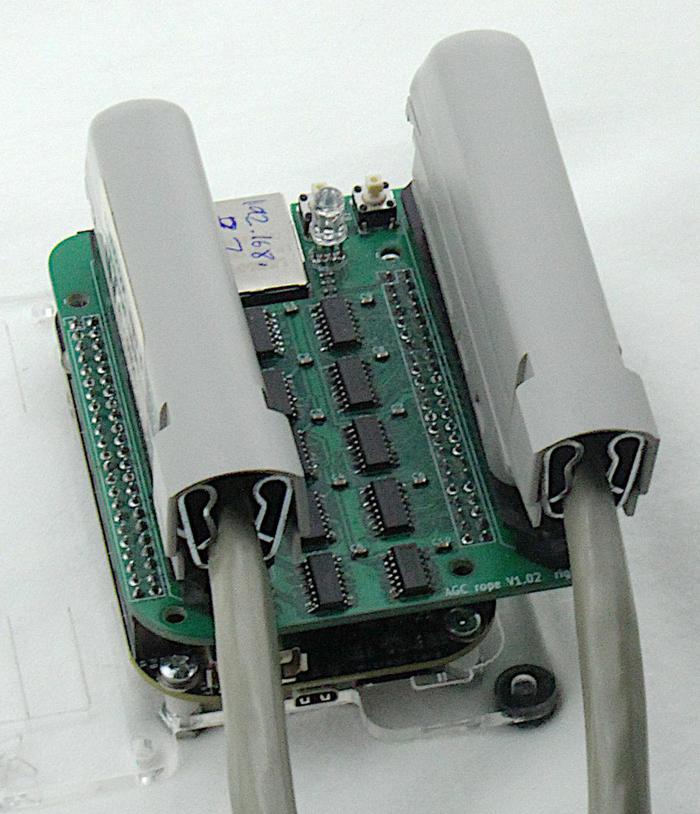
The Apollo Guidance Computer powered up. The cover is off, showing the computer's purple wire-wrap wiring of the backplane. We built the interfaces that are plugged into the front of the computer. At the back, vintage core rope simulator boxes are visible in the core rope slots.

The Apollo Guidance Computer powered up. The cover is off, showing the computer's purple wire-wrap wiring of the backplane. We built the interfaces that are plugged into the front of the computer. At the back, vintage core rope simulator boxes are visible in the core rope slots.

The Apollo Guidance Computer was developed in the 1960s for the Apollo missions to the Moon. Onboard the Apollo spacecraft, these computers provided guidance, navigation, and controlled the engines. In an era when most computers ranged from refrigerator-sized to room-sized, the Apollo Guidance Computer was small enough to fly in space. One of the very first computers to use integrated circuits, the AGC was 70 pounds and under a cubic foot in size.

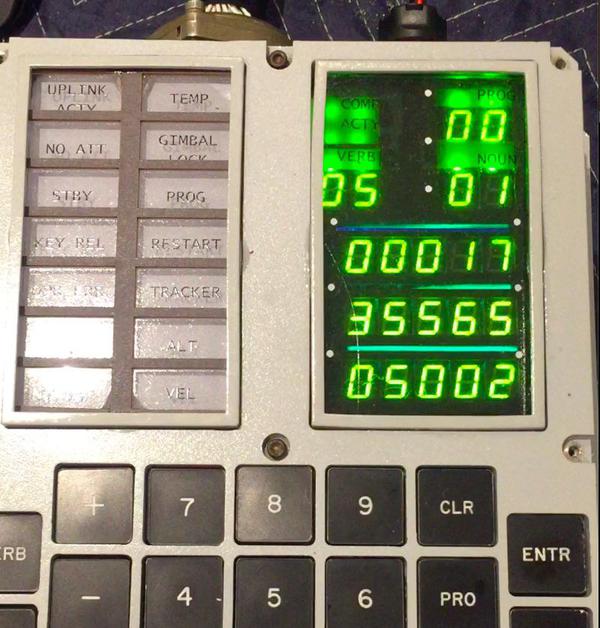
The output from the Bitcoin mining program, displayed on the Display/Keyboard (DSKY).
The display shows part of the Bitcoin hash in octal.
The DSKY is a modern replica, hooked up to the genuine AGC.

The output from the Bitcoin mining program, displayed on the Display/Keyboard (DSKY). The display shows part of the Bitcoin hash in octal. The DSKY is a modern replica, hooked up to the genuine AGC.

The Apollo Guidance Computer also pushed the boundaries of software engineering under the leadership of Margaret Hamilton. It had a cutting-edge real-time operating system that supported multiple prioritized jobs2 along with fault detection and handling. Much of the software was in assembly language but the AGC also had an interpreter designed for navigation algorithms. The interpreter implemented a virtual machine that provided vector and matrix arithmetic along with trigonometry and double- and triple-precision numbers.

How Bitcoin mining works

As the leading digital currency, Bitcoin has received a lot of attention in the past few years. The Bitcoin system can be thought of as a ledger that keeps track of who owns which Bitcoins, and allows them to be transferred from one person to another. The revolutionary feature of Bitcoin is there's no central machine or authority keeping track of things. Instead, the records are spread across thousands of machines on the Internet, and the system works with nobody in charge.

To ensure everyone agrees on which transactions are valid, Bitcoin uses a process called mining—about every 10 minutes a block of outstanding transactions is mined, which makes the block "official". Bitcoin mining is designed so it takes an insanely huge amount of computational effort to mine a block, so nobody can take over the mining process. Miners compete against each other, generating trillions and trillions of random "hashes" until someone finds a lucky one that starts with 18 zeros.3 This hash forms a successfully mined block, and then everyone moves on to the next block. The idea is that getting 18 zeros in a row randomly is extremely unlikely, so it takes a huge number of tries before someone succeeds. It's kind of like a lottery, where miners keep trying until someone "wins", but finding a valid hash is less likely than finding a single grain of sand out of all the sand on Earth.

Each time a block is successfully mined, new Bitcoins are created; currently, a successful miner gets 12.5 new Bitcoins (worth $140,000) as well as transaction fees. The possibility of receiving $140,000 every 10 minutes motivates miners to build datacenters full of specialized hardware using huge amounts of electricity.4

Structure of a Bitcoin block

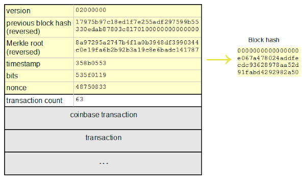
Structure of a Bitcoin block. The data in yellow is hashed to yield the block hash, which becomes the identifier for the block. The block is linked to the previous block by including the previous block's hash, forming the blockchain. The Merkle root is a hash of all the transactions in the block.

The diagram above shows what actually goes into a block that is mined. The yellow part is the block header (which gets hashed), and it is followed by the transactions that go into the block. Each block contains the hash of the previous block, causing all the blocks to be linked together forming the blockchain. On the right, you can see that the hash above was successful because it starts with lots of zeros.

To summarize the mining process: you collect new Bitcoin transactions and create a header as in the diagram above. You generate the cryptographic hash of the block. If by some incredible chance the result starts with 18 zeros you send the block into the Bitcoin network and "win" $140,000 in Bitcoin. Otherwise, you change the header slightly and try again as fast as possible. When someone else succeeds in mining the block, you start over from the new block and new transactions.5

The SHA-256 hash algorithm used by Bitcoin

Where do these hashes come from? Bitcoin mining is based on cryptography, with a "hash function" that converts a block of data into an essentially random hash value. The hash algorithm is designed to be simple to implement, but cryptographically secure: there's no known short cut to finding a successful hash other than trying zillions of hashes through brute force. In particular, Bitcoin uses a standard cryptographic hash function called SHA-256.6 This algorithm is so simple you can literally do it by hand, but it manages to scramble the data entirely unpredictably.

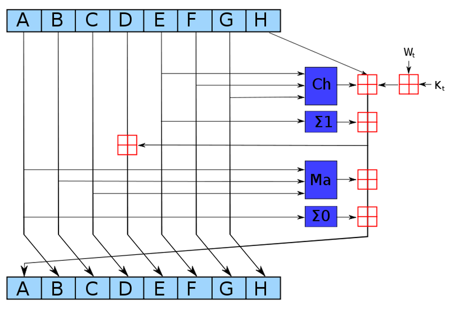
The SHA-256 algorithm can be described in about a page of pseudocode. It consists of a scrambling step called a "round", repeated 64 times. The diagram below shows one round, which takes eight 4-byte hash values, A through H, performs a few operations, and generates new values for A through H. As can be seen from the diagram, only A and E are changed in a round, while the others are just shifted over. Even so, after 64 rounds the input data will be completely scrambled, generating the unpredictable hash output.

This diagram shows the computations during one round of SHA-256. This process is repeated 64 times. Source: Wikipedia created by kockmeyer, CC BY-SA 3.0.

This diagram shows the computations during one round of SHA-256. This process is repeated 64 times. Source: Wikipedia created by kockmeyer, CC BY-SA 3.0.

The operations in SHA-256 are simple bit operations. The red boxes above indicate 32-bit addition, generating new values for A and E. The Ch "choose" box chooses bits from F or G, based on the value of input E. The Σ "sum" boxes rotate and sum bits. The Ma "majority" box looks at the bits in each position of A, B, and C, and selects whichever value is in the majority. The Kt values are constants. The input data enters the algorithm through the Wt values. These operations can be easily implemented on a computer using simple arithmetic and logic operations.7 (The operations can also be easily implemented in a custom logic circuit, which is why Bitcoin mining chips are popular.)

The Apollo Guidance Computer's processor

The AGC doesn't have a microprocessor, as it was built years before microprocessors were developed. Instead, the processor is built from about 5600 NOR gates. These gates were combined to make circuits such as flip flops for registers, binary adders, control logic, and so forth. The AGC was one of the first computers to use integrated circuits; each integrated circuit held two NOR gates. The computer had 24 logic modules similar to the one below. Each logic module had 120 integrated circuits (240 NOR gates). For example, the registers and ALU were implemented with four modules, each implementing 4 bits of the processor.

A logic module from the Apollo Guidance Computer. The module consists of 120 integrated circuits, each one implementing two NOR gates. Photo courtesy of Mike Stewart.

A logic module from the Apollo Guidance Computer. The module consists of 120 integrated circuits, each one implementing two NOR gates. Photo courtesy of Mike Stewart.

The computer's architecture was unusual by modern standards: it used a 15-bit word, along with parity. (Back then, computers often had a word size that fit the application, not necessarily a power of 2.) The AGC had just 2K words of RAM, along with 36K words of ROM. Its ROM was constructed from core rope memory. (I wrote about the AGC's RAM core memory here and core rope here).

The Apollo Guidance Computer was slow even by 1960s standards; it could perform about 40,000 additions per second. (In the AGC's defense, this was an era when most computers ranged from refrigerator-sized to room-filling, so the AGC did well for its size.) The AGC's main strength was I/O: it had hundreds of I/O connections to provide real-time control of the spacecraft.

Implementing SHA-256 on the Apollo Guidance Computer

My implementation of the SHA-256 hash algorithm implementation follows the pseudocode pretty closely. I ran into some difficulties, though, since the AGC's instruction set lacks many features of modern computers. For instance, the AGC (like many 1960s computers) didn't have a stack, so you had to keep track of the return address for each subroutine call.

Another complication was that the SHA-256 algorithm uses 32-bit unsigned numbers, while the AGC used 15-bit signed numbers in obsolete 1's complement form, so even addition required some tricky code. To fit a 32-bit number into the AGC, I split each word into a 4-bit chunk and two 14-bit chunks. (I used 14-bit chunks and not 15-bit chunks because I needed to use unsigned arithmetic.)

The next issue was that the AGC has very limited memory. The AGC, like most computers of the 1960s, used magnetic core memory, storing each bit in a tiny magnetized ferrite ring. Since core memory was fairly bulky, the AGC had just 2K words (approximately 4K bytes) of RAM. The AGC's addressing scheme made things more complicated since you could only access 256 words unless you used an inconvenient bank switching mechanism. The problem is that the SHA-256 algorithm uses eight (32-bit) hash values, a 64-word message table, and 8 words of intermediate values. These three arrays alone used up 240 AGC words, leaving about 16 words for everything else (temporary values, subroutine return addresses, loop counters, pointers, etc.) I managed to get everything to fit in one bank by reusing these 16 words for multiple purposes, but I spent a lot of time debugging problems when a variable clobbered a location still in use.

For RAM, the Apollo Guidance Computer used this 2 kiloword core memory module.

For RAM, the Apollo Guidance Computer used this 2 kiloword core memory module.

Most modern computers have shift and rotate instructions to manipulate words, but the AGC instead used three special registers. Writing to a special register would cycle the value right one bit, shift the value right, or cycle the value left. The SHA-256 algorithm uses many 32-bit shifts and rotates, which I had to convert into loops using the 15-bit cycle register. The point is that a shift operation like x>>10 is trivial in C, but I needed to implement a whole subroutine to do it on the AGC.

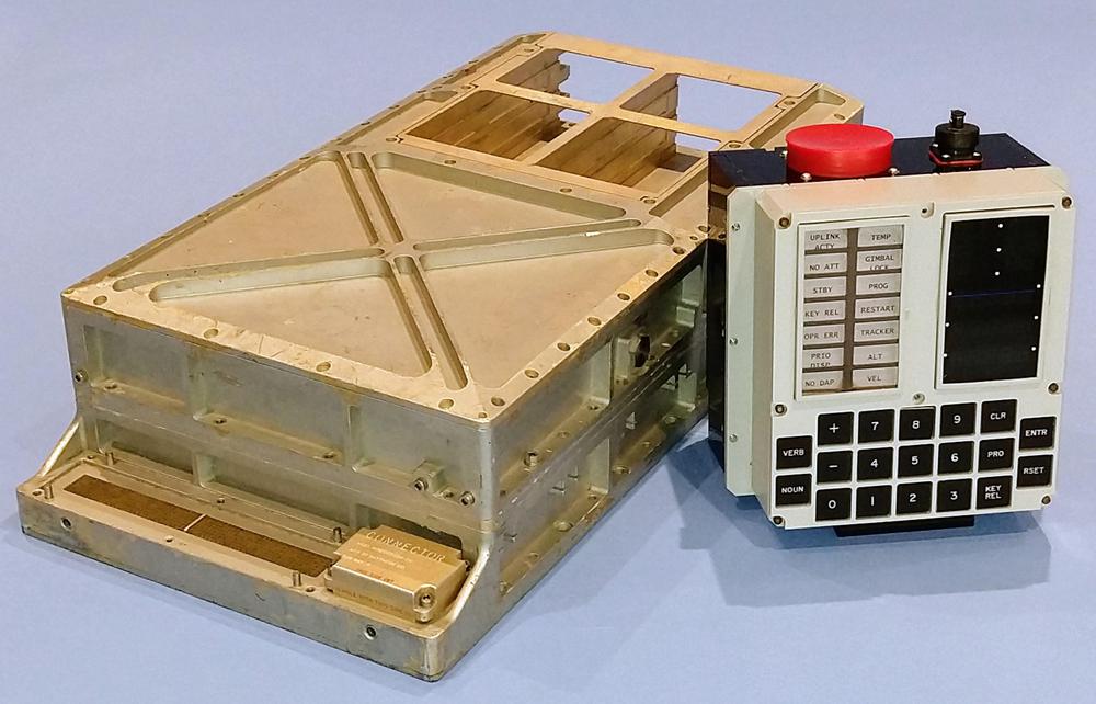
Our Apollo Guidance Computer and replica DSKY. The computer's I/O connectors are visible at the front of the computer. six core rope slots at the back are empty. The photo is an homage to this classic AGC photo.

Our Apollo Guidance Computer and replica DSKY. The computer's I/O connectors are visible at the front of the computer. six core rope slots at the back are empty. The photo is an homage to this classic AGC photo.

To keep the instruction set and code size small, the AGC had some instructions with side effects you wouldn't expect. For example, the TS (Transfer to Storage) instruction wrote a value to memory, which seems straightforward. But if the previous addition had an overflow (i.e. a carry), TS also skipped the next instruction and loaded the accumulator with a +1 or -1. In other words, simply writing a value to memory could result in a jump in control flow and register modification. The purpose of this was to handle carries for multiple-precision arithmetic, but most computers simply implement this with an "Add with carry" instruction.

Running the program

The video below shows my Bitcoin program running on an actual Apollo Guidance Computer with the results displayed on our DSKY (Display/Keyboard). The DSKY had a simple numeric keypad with buttons large enough for astronauts to use with gloves on. The computer displayed output numerically; astronauts had to know if the output was feet, seconds, degrees, or something else. We used a replica DSKY created by Carl since nobody would let us use a real DSKY.8

The Apollo Guidance Computer had a very simple user interface through the DSKY. An astronaut selected an action pressing the "Verb" key, entering a verb number, and pressing "Enter". The astronaut selected a target for the action by entering a "Noun". (Astronauts had a reference card listing all the verbs and nouns.) I added Bitcoin mining as Verb 65 in a program called Borealis9; you can see Mike enter Verb 65 at the beginning of the video.

The Apollo Guidance Computer took 5.15 seconds for one SHA-256 hash. Since Bitcoin uses a double-hash, this results in a hash rate of 10.3 seconds per Bitcoin hash. Currently, the Bitcoin network is performing about 65 EH/s (65 quintillion hashes per second). At this difficulty, it would take the AGC 4×10^23 seconds on average to find a block. Since the universe is only 4.3×10^17 seconds old, it would take the AGC about a million times the age of the universe to successfully mine a block.

Given the astronomical difficulty of mining, you might wonder how I successfully mined a block. For this demonstration, I simply used as input a block that had been successfully mined in the past, specifically block #286819. Thus, the algorithm succeeded quickly, but since it was an old block, I didn't make any money off it.

To put the AGC's mining performance in perspective, a USB stick miner performs 130 billion hashes per second. The stick miner costs under $70, compared to $150,000 for the Apollo Guidance Computer. For its time, the Apollo Guidance Computer was an extremely compact, low-power system, using 55 watts and taking up under a cubic foot of space. The USB miner, though, uses 12 watts and fits in your hand. The enormous difference in performance is due to the exponential increase in computer speed described by Moore's law as well as the advantage of custom Bitcoin mining hardware.

Programming the AGC—then and now

In the 1960s, code for the AGC was written on punch cards, and assembled onto tape using a software system called YUL. This system was more advanced than you'd expect for the 1960s, including a source control system to track and incorporate changes. For flight, the software was woven into core ropes, with wires physically going around cores for a 0 or through cores for a 1. In other words, each core rope was custom-manufactured, with the data stored in the weaving pattern of the wires. This provided high-density, reliable ROM storage, but required weeks of manufacturing.

Detail of core rope memory wiring from an early (Block I) Apollo Guidance Computer. Photo from Raytheon.

Detail of core rope memory wiring from an early (Block I) Apollo Guidance Computer. Photo from Raytheon.

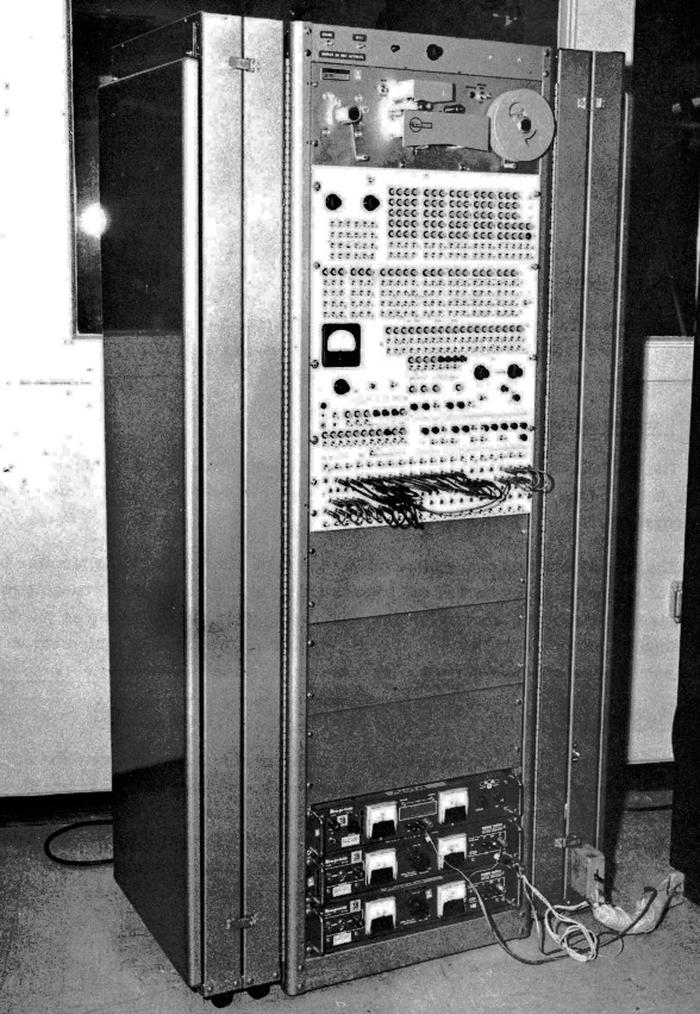
Since it wasn't practical to manufacture a new core rope for every change, a different approach was used during development. A core rope simulator allowed a program to be fed into the AGC from external storage. This simulator was part of the refrigerator-sized monitor (below), which provided a debugging interface to the AGC through a test connector on the AGC. The monitor allowed programmers to set breakpoints, single-step, examine registers, and so forth, using lights and switches.

The AGC monitor provided a debugging interface to the AGC as well as a core rope simulator. See User's guide to the AGC monitor.

The AGC monitor provided a debugging interface to the AGC as well as a core rope simulator. See User's guide to the AGC monitor.

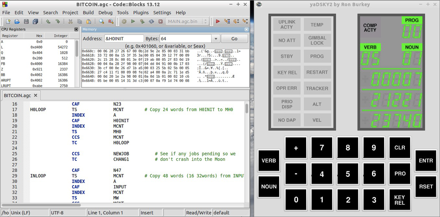
In my case, I wrote the software on my laptop and assembled it with yaYUL, a modern version of YUL written by the Virtual AGC team. I tested the software on a simulated AGC using the Code::Blocks IDE11, which provides debugging features somewhat similar to what the monitor provided in the 1960s. To run the code on the real AGC, we obviously didn't manufacture core ropes. We have vintage core rope simulator boxes, but they turned out to be extremely unreliable. Fortunately, Mike Stewart built a board to load code into the AGC using the same AGC test connector originally used by the monitor.

AGC code can be developed in an IDE. The debugger makes it much easier to develop code. The IDE communicates with the virtual DSKY.

AGC code can be developed in an IDE. The debugger makes it much easier to develop code. The IDE communicates with the virtual DSKY.

Conclusion

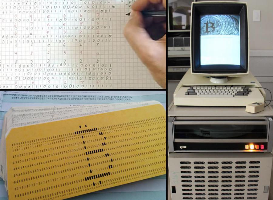
I implemented the SHA-256 hash algorithm and ran it on the Apollo Guidance Computer that we're restoring, taking 10.3 seconds per hash. This isn't my first experiment with absurd Bitcoin mining. I tried mining by hand with pencil and paper; this had a hash rate of 0.67 hashes per day. Using an IBM punch card mainframe computer from the early 1960s got the hash rate up to 80 seconds per hash. My fastest implementation was on a Xerox Alto (the famous 1973 computer that inspired the Macintosh), which performed 1.5 hashes per second. Thus, the Apollo Guidance Computer outperformed the older transistor-based IBM computer but not the Alto.

My Bitcoin mining experiments by hand, on a punch-card mainframe, and on a Xerox Alto.

My Bitcoin mining experiments by hand, on a punch-card mainframe, and on a Xerox Alto.

The Apollo program cost 25.4 billion dollars as of 1973, equivalent to about 150 billion dollars today. The current market cap of Bitcoin is 200 billion dollars, so if NASA had been mining Bitcoins, they could have paid for the whole Apollo program and still had money left over. One flaw in this plan is the Apollo Guidance Computer's low performance, since mining a block would take much more than the lifetime of the universe.

My code is available on Github; the mining code is in BITCOIN.agc. CuriousMarc has a series of AGC videos which you should watch for more information on the restoration project. I announce my latest blog posts on Twitter, so follow me @kenshirriff for future articles. I also have an RSS feed. Thanks to Mike Stewart for supplying images and extensive information.

Notes and references

  1. The AGC restoration team consists of Mike Stewart (creator of FPGA AGC), Carl Claunch, Marc Verdiell (CuriousMarc on YouTube) and myself. The AGC that we're restoring belongs to a private owner who picked it up at a scrap yard in the 1970s after NASA scrapped it. For simplicity, I refer to the AGC we're restoring as "our AGC".

    The Apollo flights had one AGC in the command module (the capsule that returned to Earth) and one AGC in the lunar module. In 1968, before the Moon missions, NASA tested a lunar module with astronauts aboard in a giant vacuum chamber in Houston to ensure that everything worked in space-like conditions. We believe our AGC was installed in that lunar module (LTA-8). Since this AGC was never flown, most of the modules were not potted with epoxy. 

  2. Because the AGC supported multiple programs at once, my code needed to periodically call NEWJOB to see if there were any other waiting jobs to run. To ensure reliability, the AGC constantly checked to make sure a faulty program doesn't take over the system. Thus, I needed to give other jobs the chance to run or else my job would get killed. 

  3. At the current Bitcoin difficulty level, about 1 in 10^22 hashes will be successful at mining a block; a valid hash must start with approximately 18 zeros. The mining difficulty changes periodically to keep the time between blocks at approximately 10 minutes. As mining hardware gets faster, the difficulty factor is automatically updated to make mining more difficult so miners can never really catch up. 

  4. A while back I estimated that Bitcoin mining uses about as much electricity as the entire country of Cambodia. One paper puts mining's energy consumption comparable to Ireland's electricity usage. A recent estimate is that Bitcoin mining uses more electricity than Switzerland. 

  5. I've simplified a lot of details in my discussion of Bitcoin algorithms. For in-depth information on Bitcoin and mining, see my articles Bitcoins the hard way and Bitcoin mining the hard way

  6. Bitcoin uses "double SHA-256" which simply consists of applying the SHA-256 function twice. I could have implemented the double-hash in the AGC code, but I ran out of time; I got the basic hash working at 4 am the night before we sent the AGC back to Houston. How to upload transactions into the AGC is also left as an exercise for the reader. 

  7. While SHA-256 is easy to implement, that's not the case for all the cryptography used by Bitcoin. To create a Bitcoin transaction, the transaction must be signed with elliptic curve cryptography. This requires 256-bit modular arithmetic, which is about as hard as it sounds. Even a simple implementation is 1000 lines of C. Needless to say, I decided not to implement signing in assembly language on the AGC. 

  8. Many people have asked if we talked to Fran Blanche about the DSKY. Yes, we have. 

  9. The Aurora program was used to extensively test the operation of the Apollo Guidance Computer in the Lunar Module. I wrote the Bitcoin code as part of Borealis, a modern version of Aurora slightly cleaned up. The code for Aurora and Borealis includes a table of verb definitions so it was straightforward for me to add Verb 65 for my Bitcoin code. In the video, you can see Mike enter Verb 65 to start the Bitcoin program. I also took advantage of the Executive's octal display routine to show the output. This routine is accessed through Verb 05 Noun 01, which is why you'll see that on the display at the end of the video. 

  10. At the end of the video clip, the display shows 8 octal triples indicating the hash: 00000/00000/00000, 00000/00000/00000, 00007/21221/23740, 00017/35565/05002, 00002/20333/04715, 0o00002, 0o33226, 0o05227, 00004/05367/35221, 00005/00252/14222. (The 11111/11111/11111 value is just a signal that all values have been displayed.) Converting these to hex and reversing the bytes yields the 8-byte Bitcoin hash: 00000000 00000000 e067a478 024addfe cdc93628 978aa52d 91fabd42 92982a50. Note the multiple zeros at the beginning of the hash; this is what makes the hash valid. 

  11. The Virtual AGC project has developed simulations of the AGC, DSKY, and YUL assembler, so you can experiment with the AGC system. While you can do this from the command line, debugging is much, much easier if you use the Code::Blocks IDE. You can download a VirtualBox environment with everything set up here. In the folder "AGC Visual Debugging", double-click on Borealis to start Code::Blocks. You can edit code in the IDE (or with an editor). Then "Build → Build" compiles the code and "Debug → Start" runs code in the debugger. "Tools → DSKY" starts up a DSKY window to interact with the AGC. "Debug → Debugging windows → Memory dump" lets you look at memory contents. The IDE lets you set breakpoints, single-step through code, examine memory, and so forth. For more information on AGC code development, see this page

  12. The Bitcoin protocol is a mish-mash of big-endian and little-endian values. It inconveniently reverses the byte order of the SHA-256 hash, so while the hash from the algorithm ends with zeros, the Bitcoin hash starts with zeros. I displayed the hash to match the Bitcoin order.