Repairing the card reader for a 1960s mainframe: cams, relays and a clutch

I recently helped repair the card reader for the Computer History Museum's vintage IBM 1401 mainframe. In the process, I learned a lot about the archaic but interesting electromechanical systems used in the card reader. Most of the card reader is mechanical, with belts, gears, and clutches controlling the movement of cards through the mechanism. The reader has a small amount of logic, but instead of transistorized circuits, the logic is implemented with electromechanical relays.1 Timing signals are generated by spinning electromechanical cams that generate pulses at the proper rotation angles. This post explains how these different pieces work together, and how a subtle timing problem caused the card reader to fail.

The IBM 1402 card reader/punch. The 1401 computer is in the background (left) and a tape drive is at the right.

The IBM 1402 card reader/punch. The 1401 computer is in the background (left) and a tape drive is at the right.

The IBM 1401 was a popular business computer of the early 1960s, used for applications such as payroll or inventory. Data records were stored on 80-column punch cards, which were read into the computer by the card reader and printed on the high-speed line printer. The IBM 1401's card reader (above) could read 800 cards per minute—over 13 cards per second—which is a remarkable speed for a mechanical device. Cards whizzed through the card reader, 80 metal brushes read the holes in each column, and then the cards were stacked in the hoppers in the middle of the reader.3 If anything went wrong, from a misread card to a card jam, the card reader would slam to a halt (hopefully before bent cards started piling up) and an error light would illuminate on the card reader's control panel. At this point, the operator would fix the problem and processing could continue.2

80-column punch cards. Each column of the card holds a character, represented by the holes punched in the column. THE text at the top of the card shows what is in each column. Black paper behind the first card makes the holes more visible.

80-column punch cards. Each column of the card holds a character, represented by the holes punched in the column. THE text at the top of the card shows what is in each column. Black paper behind the first card makes the holes more visible.

The photo below shows the IBM card reader/punch with the front doors opened up. The right half is the reader and the left half is the punch. (The punch records data on cards; I will ignore it in this article.) The blue panel has the operator controls and indicators. Cards enter through the feeder in the upper right, travel right-to-left through the brushes (behind the blue panel) and fall into the stacker slots (center). To the right of the stacker is the service panel with the dynamic timer (circle with knob); this will be relevant later. The relays, resistors, capacitors and diodes that make up the reader's circuitry are below the service panel. Converting the hole pattern to characters was done by the 1401 computer, not the reader, so this circuitry is fairly basic.3 The garbage can on the lower left collects "chips", the bits punched out of cards by the punch, and triggers a warning light when it is full.

With the front doors of the card reader/punch removed, the circuitry is visible. The left half is the punch and the right half is the reader. The *Reader Stop* light is illuminated on the panel, indicating a malfunction.

With the front doors of the card reader/punch removed, the circuitry is visible. The left half is the punch and the right half is the reader. The *Reader Stop* light is illuminated on the panel, indicating a malfunction.

A few months ago a problem with the card reader kept showing up under certain circumstances: the card reader would halt with a "Reader Stop" error, indicating a problem with card feeding and travel.2 Given the age of the card reader at the Computer History Museum, it's not surprising that Reader Stop problems arise. However, in this case, cards were feeding fine and there was nothing visibly wrong. Eventually the 1401 maintenance team determined that the problem occurred if you do multiple cycles of reading a card, printing a line on the printer, reading a card, printing a line, and so on. The first three cards read fine, but the fourth card read always failed with a Reader Stop. But during normal processing, hundreds of cards could be read without a problem. What was different about repeatedly reading and printing?

The card reader can read 800 cards per minute, but the line printer can only print 600 lines per minute. Thus, if you continuously read and print, the printer will eventually fall behind. The consequence is that the card reader will occasionally be blocked while the printer finishes a line. In particular, the system can read and print three cards in a row, but there is a delay before reading the fourth card.4 This is normal behavior for the system, but for some reason, this delay was triggering the Reader Stop error.

The question at this point of the investigation was why the delayed read triggered a Reader Stop. The logic diagram below shows the many different things can cause a Reader Stop.5 (This logic was implemented in the reader by relay circuits of Byzantine complexity.) Usually a card jam or card feed problem is responsible for a stop, but there weren't any card movement problem. And the card levers (microswitches) that detect card movement were operating correctly. Eventually, the team discovered that removing relay R-10 (Read Clutch Impulse near the bottom of the diagram) stopped the Reader Check from happening. Removing this relay prevented the clutch status from being checked8 so it prevented the error from being reported but didn't fix the underlying problems. It did, however, indicate that the problem was with the clutch.

Diagram showing the logic conditions that yield a Reader Stop error in the card reader. From the manual.

Diagram showing the logic conditions that yield a Reader Stop error in the card reader. From the manual.

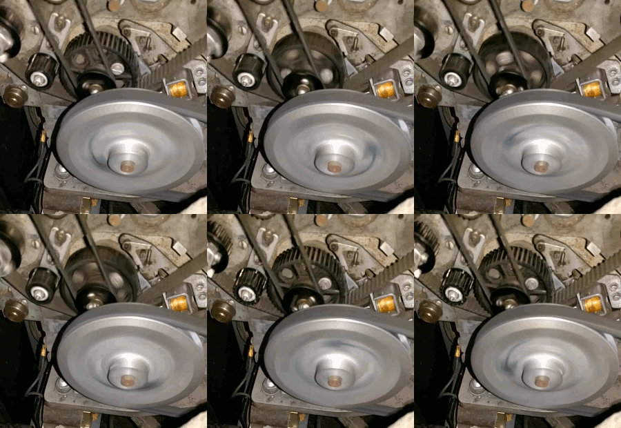
At this point, I'll explain how the clutch works in the card reader. The card reader is powered by a 1/4 horsepower electric motor. This motor powers a variety of shafts, belts, rollers and cams inside the card reader. However, the reader needs a mechanism to rapidly start and stop card reading under computer control. This is accomplished by a clutch that powers the card feed rollers. With the clutch engaged, cards will be fed through the card reader. With the clutch disengaged, cards will not move (although other parts of the reader will keep running). The GIF below shows the clutch in action: it is disengaged for one cycle and engaged for one cycle. Although the silver pulley (driven by the motor) turns continuously, the black gear is started and stopped by the clutch, which is just behind the black gear.

The clutch in the 1402 card reader. The clutch is disengaged for one cycle and engaged for one cycle.

The clutch in the 1402 card reader. The clutch is disengaged for one cycle and engaged for one cycle.

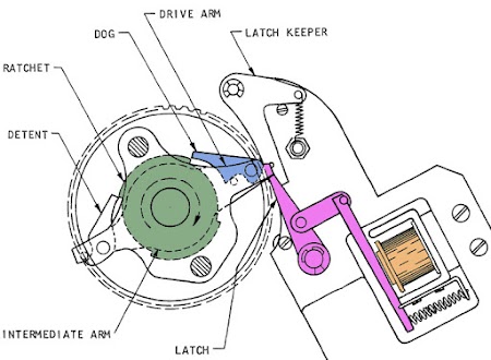
The diagram below shows the main parts of the clutch. The ratchet (green) continuously rotates, powered by the motor. When the coil (orange) pulls the latch (purple), the dog (blue) will fall into the ratchet (green), engaging the clutch. This will cause the outer wheel to rotate in sync with the ratchet, feeding a card. After one cycle, the clutch can be disengaged by the latch, or can remain clutched for another cycle. Above, you can see the latch move just before the clutch engages. The dogs and ratchet are hidden behind the black gear. For more details, see the footnotes.67

The card reader's clutch mechanism. From the 1402 manual.

The card reader's clutch mechanism. From the 1402 manual.

The clutch requires careful timing. If the coil pulls the latch too late, the dog won't engage with the ratchet until the next cycle and no card will be fed. And if the latch is released too late, the clutch won't disengage until the next cycle, feeding an extra card. Either way, this would cause a serious problem if you are, for instance, printing payroll checks. To catch this, the card reader includes a clutch check circuit that ensures that a clutch happens only when requested.8 This circuit is what triggered the Reader Stop issue.

Timing in the card reader is controlled by the angular position of the main drive shaft; there isn't a clock signal. A 360° rotation of the drive shaft corresponds to one card read cycle.9 The mechanical and electrical components must be precisely adjusted so they activate at the correct rotational angles. For instance, a card's first row of holes reaches the brushes at 8° and card lever #1 is triggered at 227°. And the clutch is engaged or disengaged at exactly 315°. Electrical signals are generated by rotating cams that open and close microswitches at the appropriate degree angles. For example the read clutch is controlled by cam RC6 that closes at 272° and opens at 342°. The photo below shows a cam on a drive shaft, with the microswitch above it; when the cam rotates to a high point, the switch closes.

One of the cams and microswitches in the card reader.

One of the cams and microswitches in the card reader.

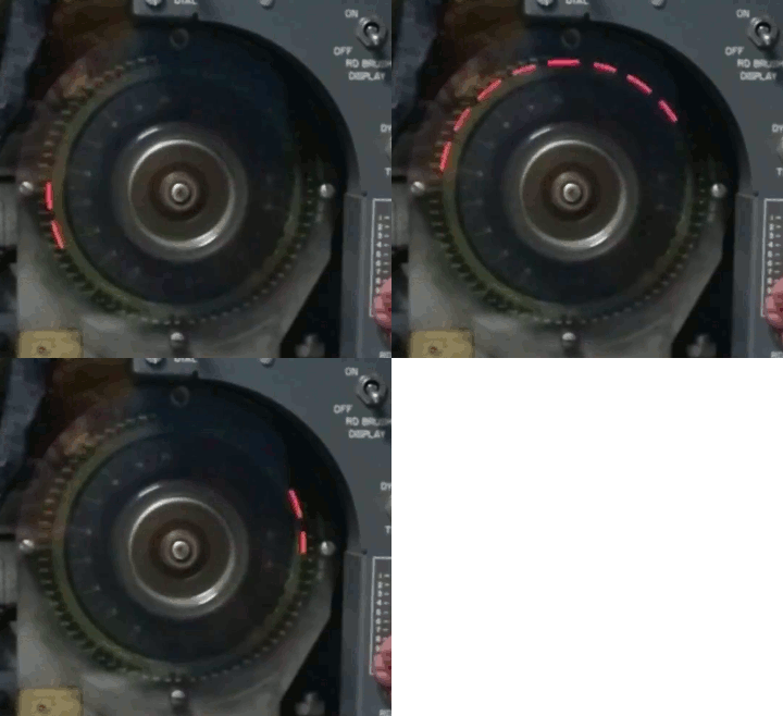
To examine timings, the card reader has an interesting maintenance feature called the Dynamic Timer, which is sort of a mechanical oscilloscope that visually shows the angle timing of signals. The dynamic timer consists of a neon bulb that spins behind a plastic disk labeled with the angles from 0° to 359°. If a signal is selected with a control panel switch, the bulb lights up when the signal is active.1 Because the neon bulb is spun by the main driveshaft, its position is synchronized to the rotation angle of the card reader's mechanisms. Thus, the neon bulb traces out sectors of a circle, indicating when the signal is active. For example, the image below shows the read brush signal, which is activated as each card row passes under the brushes. Since there are 12 rows on a punch card, the signal is activated 12 times in a card cycle. By reading the angle labels on the clear plastic dial, the signal timings can be checked for correctness. In addition, the knob in the middle of the dynamic timer can be rotated manually to move the card reader's cycle to any desired angle.

The dynamic timer of the 1402 card reader. The 12 signals correspond to the 12 rows on the card, indicating when the row passes through the brushes.

The dynamic timer of the 1402 card reader. The 12 signals correspond to the 12 rows on the card, indicating when the row passes through the brushes.

We measured the timing of read clutch control cam RC6 and found it was off by about 5 degrees. The manual called the timing of this cam "critical" saying it needed to be within 2° earlier or 0° later from the correct angle.10 Since the cam was well outside the allowed range, we tried to adjust it. The first problem was that the cam was frozen to the shaft; apparently after decades of storage in a a damp garage it had rusted to the shaft. Carl eventually hit the cam hard enough (yet carefully!) with a hammer to loosen it from the shaft so it could be adjusted.

The photo below shows how we manually adjusted cam timings. The dynamic timing wheel (left) can be turned by hand until the cam closes, and then the angle can be read from the dial. The adjustment process is rather tedious, requiring trial and error. First, the duration that contact is closed is corrected by moving the contact closer or farther from the cam. After each adjustment, the duration must be manually checked by slowly rotating the dynamic timing wheel 360°. Once the duration is correct, the next step is to rotate the cam a few degrees at a time until it closes and opens at the right angle. Again, the timing must be carefully checked after each adjustment until trial-and-error yields the right cam setting.

By manually rotating the dynamic timer wheel, the cam timing (center) can be checked. The light (upper right) shows when the cam has closed. This photo shows cam RL10 being adjusted.

By manually rotating the dynamic timer wheel, the cam timing (center) can be checked. The light (upper right) shows when the cam has closed. This photo shows cam RL10 being adjusted.

Once cam RC6 had the proper timing, we tested the card reader. Surprisingly, it failed just as before. We checked the timing of RC6 with the dynamic timer, and strangely, the timer still showed that it closed 5° too late, even though we had measured it as closing correctly. After puzzling over the schematics, I found that cam RC6 was powered through cam RL10, so a bad timing on cam RL10 would cause the dynamic timer to show the wrong time for RC6.

We continued the next week and measurement of RL10 showed it was closing 5° too late. So we repeated the cam adjustment process with RL10. Carl loosened RL10's setscrews, whacked it with a hammer, and was surprised when it spun around on the shaft—apparently it hadn't rusted onto the shaft the way RC6 had. Since the timing of RL10 was now thoroughly off, it took some extra effort to find the right position for it. One complication is that RL cams only rotate while the clutch is tripped, so we had to manually trip the clutch for each test. (This video shows how the clutch can be tripped manually.) After a couple hours of adjustment, the cam had the right duration and then the right start angle.

We powered up the card reader and this time it ran all the tests successfully! We had found the elusive problem. Apparently cam RL10 was open a bit too much, so the signal to read a card after a pause in reading wasn't quite able to engage the clutch. Then the clutch check circuitry would detect that the clutch had failed to engage, triggering the Read Stop.

Conclusion

Tracking down and fixing the mysterious Reader Stop errors on the card reader was tricky and more time-consuming than most problems. But it provided an interesting look back in time at the obsolete technology used inside the card reader: relay logic, spinning cams and a mechanical clutch. Debugging the card reader is a different experience from tracking down software problems or even normal hardware problems. Just understanding the schematics with their obsolete symbols can be a challenge. Hopefully what we learned in this repair will help us the next time the card reader malfunctions.

Many members of the 1401 restoration team were involved in fixing this problem, including Carl, Frank, Alexy, Ron, George, Glenn, Jim and Grant. The Computer History Museum in Mountain View runs demonstrations of the IBM 1401 on Wednesdays and Saturdays so check it out if you're in the area; the demo schedule is here.

Follow me on Twitter or RSS to find out about my latest blog posts.

Notes and references

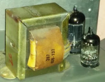
  1. While IBM's computers were supposed to be transistorized by the time of the 1401, two vacuum tubes are hidden deep inside the card reader. These tubes power the neon bulbs for the dynamic timer used for diagnostics. The photo below shows the tubes and the transformer that powers them.

    The 1402 card reader contains two vacuum tubes to drive the neon bulbs in the dynamic timer.

    The 1402 card reader contains two vacuum tubes to drive the neon bulbs in the dynamic timer.

  2. The 1402 card reader reports three types of errors. A Reader Stop indicates a jam or card feed problem. (This is the error we encountered.) A Validity error indicates an invalid character caused by a bad hole pattern. A Reader Check indicates that the card was read incorrectly. An interesting technique was used to detect a bad read. The first set of brushes was used to count the number of holes in each column. The second set of brushes performed the actual read of the characters. If the number of holes in a column was different between the first and second reads, the system knew that the card had been read incorrectly. (This was typically caused by a brush that was slightly out of alignment or making bad contact.) You might wonder why the holes were counted, instead of just checking the characters. Counting holes required fewer bits of expensive core memory. 

  3. The card reader itself didn't convert the hole pattern into characters. Instead, there were 80 parallel wires directly from the 80 hole-sensing brushes to the computer, which did the hole-to-character conversion. The reader had one set of brushes to count holes (for the error check) and a second set to actually read the characters. The punch had a set of brushes to check the punched holes and optionally a set of brushes to read before punching. Thus, there could be up to four sets of brushes in the reader/punch. In addition, the punch had 80 wires from the computer to the 80 hole punch coils. As a result, two massive 200-wire cables connected the card reader and the computer. 

  4. The 1401 computer has a core-memory print buffer that allows computation to continue while printing a line. However, a complex interlock circuit will block the computer if it tries to print a line while the buffer is still in use. (This buffering and locking is all done in hardware; there is no operating system.) The print buffer was an optional feature for the computer, renting for an extra $386 per month. 

  5. The Reader Stop diagram shown earlier is somewhat confusing, but I'll give an overview. As cards pass through the card reader, they trip microswitches (called Card Levers or CLC). The logic tests if a microswitch isn't triggered, indicating if a card got jammed before reaching the microswitch. For example, the second triangle triggers an error if there are cards in the hopper, but no card reached card lever 1 after a feed signal. (Note that the logic symbols are backwards compared to modern usage; IBM used a semicircle for OR, and a triangle for AND. Thus, each set of inputs into a triangle shows a set of conditions that will trigger a reader stop.)

    A label like R-6 indicates that the signal comes from relay 6. Relay R-13 is the Reader Stop Control relay; it gets triggered if there was a card at microswitch 1 or 2 during angle 158°-188°. During this time, the card should have already passed the microswitch, so if it is still closed, there must be a jam. "CLC 1 DELAY" indicates that there was a card at CLC 1 in the previous cycle. If there is no card at CLC 2 this cycle, the card must have been jammed along the way. 

  6. Several documents on the 1402 card reader/punch are available on bitsavers. The IBM 1402 Card Read-Punch Manual is an operator's manual for the card reader. The Customer Engineering Manual of Instruction explains the implementation of the card reader for the service engineer, and is probably the best guide to how it operates. The Customer Engineering Instruction Reference Manual explains the internals of the card reader, with a focus on maintenance. The Wiring Diagram provides schematics of the card reader. The Service Index provides a summary of information for servicing. 

  7. The operation of the clutch mechanism is a bit tricky. In the diagram below, the ratchet (green) is constantly spinning. The remaining parts of the clutch are connected together and rotate only when the clutch is engaged. The key idea is that when the intermediate arm (middle) is latched, the control studs push the dogs up and out of the ratchet disengaging the clutch. (This happens because the intermediate arm can pivot slightly relative to the drive arm (left), so the dog pivot and control stud will move relative to each other, swinging the dogs upwards.) When the intermediate arm is unlatched, the dogs are no longer raised and they will engage with one of the ratchet's teeth. At this point, the mechanism is clutched and everything rotates in synchronization, until the intermediate arm hits the latch again, disengaging the dogs from the ratchet. The video of a simpler ratchet clutch may clarify the dog and ratchet mechanism.

    Diagram of the card reader's ratchet clutch, from the service manual.

    Diagram of the card reader's ratchet clutch, from the service manual.

  8. In case anyone (most likely me, in the future) needs to understand the clutch check circuit, I'll give an explanation. The reader sends a "Proc Feed" signal to the computer each time a card could be fed. If the computer wants to read a card, it sends a "Read Clutch" signal back. This signal is gated by cams RL10 and RC6 and cam RC5 and does two things. It triggers the read clutch magnet, the coil that pulls the clutch latch. It also energizes the clutch check relay R10. (See the schematic for details.) A bit later in the cycle, the clutch status is checked using the circuit below. If the clutch check relay is activated but the clutch did not latch, cam RL10 (not shown) will not be rotating and will remain closed. RL10 will trigger the Read Stop relay R4 through RC7 and R10's normally-open contacts. On the other hand, if the clutch check relay is not activated, but the clutch is latched, cam RL2 will be rotating and will trigger the Read Stop relay through the Read Stop relay R4's normally-closed contacts.

    The clutch check circuit in the card reader uses cams and relays to trigger a Read Stop if the clutch fails to latch. From the 1402 schematic.

    The clutch check circuit in the card reader uses cams and relays to trigger a Read Stop if the clutch fails to latch. From the 1402 schematic.

  9. Although one card can be read every 360° cycle of the reader, it takes three cycles to process a particular card. During the first cycle, the card is moved out of the hopper into the reader and triggers card lever 1. During the second cycle, the card passes through the first set of brushes (which counts the holes in each column), and triggers card lever 2. During the third cycle, the card passes through the second set of brushes (which actually reads the card), and is ejected into a hopper. Thus, there are typically three cards in flight in the reader at any time. (This is one reason the reader has so much circuitry to detect jams quickly, to prevent multiple cards from piling up in a crumpled heap.) 

  10. Many cams (including RC6) actually have three lobes, so they open and close three times every 360°, spaced 120° apart. This is due to an optional feature called Early Read (which cost an extra $10 per month). On the basic card reader, if the computer requests a card too late in the cycle, it has to wait for up to an entire revolution (75ms) until the clutch can latch, slowing down the system. With Early Read, there are three clutch points per revolution, cutting down the wasted time to at most 25ms. (One complication: the clutch is geared to half the speed of the regular shaft and turns 180° per cycle. This is why there are 6 teeth on the clutch ratchet.) 

IBM mainframe tube module part II: Powering up and using a 1950s key debouncer

In the 1950s, before integrated circuits or even transistors, mainframe computers were built from thousands of power-hungry vacuum tubes filling massive cabinets. To simplify construction and maintenance of these computers, IBM invented a pluggable module with eight tubes;1 failed modules could be quickly pulled out of the computer and replaced. I came across one of these tube modules and wondered if it would still work decades later. Could I power it up and demonstrate it in a circuit, or would the components have failed with time?

The glowing orange filaments are visible in the tubes of this IBM tube module. This 8-tube module is a key debouncer from the IBM 705 business computer.

The glowing orange filaments are visible in the tubes of this IBM tube module. This 8-tube module is a key debouncer from the IBM 705 business computer.

Part I of my post discussed tube modules and described the IBM 705 that used this module. To recap, the IBM 705 was a large business computer introduced in 1954. It weighed 16 tons, used 70 kilowatts of power and cost $15 million (in 2018 dollars). A few dozen 705 systems were built, mostly used by large companies and the US government. For example, Texaco2 used the 705 for accounting applications such as payroll, marketing, and distribution. Even though the 705 was intended as a business computer, Texaco also used it for technical applications such as refinery simulation and pipe stress analysis. Below you can see the large CPU of an IBM 705 computer. Each of the four panels in the front held up to 80 tube modules.

The CPU of an IBM 705. From IBM 705 Electronic Data Processing Machine brochure.

The debouncer

By tracing out the circuitry of the tube module and studying old IBM documents, I determined that the module consisted of five key debouncing circuits. When you press a key or button, the metal contacts inside the switch tend to bounce against each other a few times before closing, so you end up with multiple open/closed signals, rather than a nice, clean signal. To use a key signal in a computer, it needs to be "debounced", with the multiple rapid transitions replaced by a single, clean transition. (Perhaps you have used a cheap keyboard that occasionally gives you double letters; this happens when the keyboard bounces more than the debounce circuit can handle.) In modern systems, debouncing is usually done in software, but back in the 1950s tubes were used for debouncing.

This tube module from an IBM 705 mainframe computer, implemented five key debouncing circuits.

This tube module from an IBM 705 mainframe computer, implemented five key debouncing circuits.

The IBM 705 was controlled from a complex console with control keys and neon status lights (below). The console was used for manual control of the computer, monitoring status, detecting and correcting errors, and debugging. (While memory could be modified from the console keyboard, programs were normally read from punch cards.) Tube-based debouncing circuits were used on many of the console keys to ensure proper operation, so that's probably the role of the module I examined.3

Console of an IBM 705 computer. That console was used to control the computer and for debugging it. Photo from IBM.

Console of an IBM 705 computer. That console was used to control the computer and for debugging it. Photo from IBM.

Vacuum tubes

IBM 6211 vacuum tube: a dual triode. The pins plug into a socket on the top of the tube module. The plates are visible inside the tube. The number 6211 is faintly visible near the top of the tube.

IBM 6211 vacuum tube: a dual triode. The pins plug into a socket on the top of the tube module. The plates are visible inside the tube. The number 6211 is faintly visible near the top of the tube.

Since most readers probably haven't used vacuum tubes, I'll give a bit of background. This module was built from a common type of vacuum tube known as a triode. In a triode, electrons flow from the cathode to the plate (or anode), under the control of the grid. The heater, similar to a light bulb filament, heats the cathode to around 1000°F, causing electrons to "boil" off the cathode. The anode has a large positive voltage (+140V in this module), which attracts the negatively-charged electrons. The grid is placed between the cathode and the anode to control the electron flow. If the grid is negative, it repels the electrons, blocking the flow to the plate. Thus, the triode can act as a switch, with the grid turning on and off the flow of electrons. The module I examined used dual triode tubes, combining two triodes into one tube for compactness.

Schematic symbol for a triode tube

Schematic symbol for a triode tube

Two vacuum tube circuits form the building blocks of this tube module: the inverting amplifier and the cathode follower. The schematic below shows a vacuum tube inverting amplifier (slightly simplified). If the input to the grid is negative, the flow of electrons through the tube is blocked, and the output is pulled up to +140 volts by the resistor. If the input to the grid is positive, electrons flow through the tube, pulling the plate output close to ground. Thus, the circuit both amplifies the input (since a small input change causes a large output change) and inverts the input.

An inverting amplifier built from a vacuum tube triode.

An inverting amplifier built from a vacuum tube triode.

The second circuit used in the module is the cathode follower, which is essentially a buffer; its low-impedance output let it drive other circuits. While the schematic (below) looks similar to the inverter, it has the opposite effect since the output is from the cathode, not the plate. If a positive input voltage is fed into the grid, the tube will conduct. The voltage drop across the cathode resistor will cause the cathode voltage (and thus the output voltage) to rise. On the other hand, if the input voltage is negative, electron flow will be reduced, shrinking the voltage drop across the resistor and reducing the cathode voltage. Either way, the cathode voltage (and output) will adjust to be approximately equal to the input voltage. The trick is that it's not a negative grid per se that blocks electron flow, but a negative grid with respect to the cathode.4 Thus the cathode follower essentially copies its input voltage to the output, but providing higher current.

A cathode follower buffer built from a vacuum tube triode.

A cathode follower buffer built from a vacuum tube triode.

Powering the filaments

The first step in making the module operational was to power up the vacuum tube filaments. Filaments usually operate at 6.3V AC for historical reasons (a 6V lead-acid battery contained three 2.1V cells, yielding 6.3V). Each tube's filament uses almost 3 watts, so a large filament transformer is necessary. The filament energy consumption is part of the reason tube-based computers used so much power.

The filament transformer converts AC line input to 6.3V to power the filaments. The transformer weighs 3.5 pounds.

The filament transformer converts AC line input to 6.3V to power the filaments. The transformer weighs 3.5 pounds.

We connected the transformer and inserted tubes one at a time to power up their filaments. Everything went smoothly—the tubes all lit up with a nice orange glow and none were burnt out. Each tube has two filaments (since they are dual triodes), so we could see two orange spots in each.

The tubes give off an orange glow when the filaments are powered with 6.3V AC.

The tubes give off an orange glow when the filaments are powered with 6.3V AC.

Powering the circuitry

Powering the tube module is inconvenient because of the multiple large voltages required. This tube module uses +140V, -60V and -130V, with input signals of probably 48V.10 The power supplies we had available only went up to +/- 120V, but I did some simulations with LTspice that showed the module should work with the lower voltages. We used a stack of power supplies to power the module, mostly vintage HP supplies from Marc's collection.5

To run the tube module, we used a stack of power supplies and test equipment. Two more power supplies are under the table.

To run the tube module, we used a stack of power supplies and test equipment. Two more power supplies are under the table.

The connector for the tube module probably hasn't been manufactured in 50 years, so I needed to find a way to connect wires to the module. I could have soldered wires directly to the module, but I didn't want to modify the module since it's a historical artifact. Instead I found that .110 quick-disconnect terminals fit (more or less) on the module's pins. To manage all the connections to the tube module, I built a small junction box to connect banana plugs from the power supplies to the tube module. This box also had a button to trigger the input.6

To keep the wiring under control, I built a junction box between the power supplies and the tube module. It also includes a pushbutton to control the input.

To keep the wiring under control, I built a junction box between the power supplies and the tube module. It also includes a pushbutton to control the input.

The trigger circuit

The schematic78 below shows one of the debounce circuits, which IBM called a "contact-operated trigger". (A trigger is the old term for a flip-flop, or a similar circuit that can be in two states.) The input goes through the resistor-capacitor low-pass filter on the left, smoothing out the input so the circuit won't respond to bounces. This goes to the grid (2) of a triode inverter amplifier as discussed earlier. The output from the first inverter (plate, 1) is connected to a second inverter (grid, 7) via the 91K resistor. The output from the second inverter (plate, 6) is shifted to the desired +30/-10 voltage range by a voltage divider (the 390K and 430K resistors). Shifting the voltage down is the reason a -130V supply is needed. 6 (The two inverters form a Schmitt trigger9 due to the connected cathodes and 3K resistor.) The output from this circuit is connected to a cathode follower (described earlier but not shown in the schematic below), which buffers the signal for use by other modules.

Schematic of one "trigger" circuit of the tube module.

Schematic of one "trigger" circuit of the tube module.

The diagram below illustrates how the debouncer functions. The red line shows the input, say from a button press. Notice that the switch opens and closes twice before closing for good. If the computer used this input as a control, it might perform the operation three times. The blue line shows the debounced signal, which turns on once cleanly. To perform the debouncing, the debouncer uses a resistor-capacitor filter to smooth out (i.e. integrate) the input signal into a slowly-changing signal; this is the green line. When the green signal gets high enough; the output turns on. Note that the output stays on even though the green signal drops in the last bounce. This is due to the Schmitt trigger; it turns off at a much lower level than where it turns on.

Signals in the debouncer: red is the input (with bounce). Blue is the debounced output. Green is the internal signal after R-C filtering. This image is from an LTspice simulation of the module.

Signals in the debouncer: red is the input (with bounce). Blue is the debounced output. Green is the internal signal after R-C filtering. This image is from an LTspice simulation of the module.

Using the tube module

The tube module showing how the five debounce triggers are divided among the tubes.

The tube module showing how the five debounce triggers are divided among the tubes.

The tube module contains five debounce circuits, each made up of a trigger and a cathode follower. The diagram above shows how these circuits map onto the eight tubes. Each cathode follower (CF) uses one triode (half a tube) so there are two cathode followers per tube.11 Since there's one triode left over, the last debouncer (5) has a double cathode follower for a higher current output. The photo below shows that someone marked the top of the module with red and greed dots indicating the two tube types and functions, probably to simplify maintenance.

Top of an IBM tube module type 330567. The red dots indicate 6211 tubes and the green dots indicate 5965 tubes.

Top of an IBM tube module type 330567. The red dots indicate 6211 tubes and the green dots indicate 5965 tubes.

We tested one of the five debounce circuits in the module. Although the tube module contains five debouncers, some resistors were knocked off the module over the years, so debounce circuit 4 was the only one we could use without repairs. Below, you can see the power and signal wires hooked up to the tube module, along with an oscilloscope probe to view the output. At the left, we have wired a neon bulb to the debouncer's status output. In the computer, these status outputs were connected to neon bulbs on the console or on maintenance panels.

The tube module in operation. The filaments illuminate the tubes. At the left, a neon bulb is connected to the module's neon output.

The tube module in operation. The filaments illuminate the tubes. At the left, a neon bulb is connected to the module's neon output.

The oscilloscope trace below shows the debounce circuit in operation. The input (yellow) is a pulse with contact bounce. You can see a bunch of large spikes due to bounce, as well as couple bounces of longer duration. There is also some bouncing at the end of the pulse. In contrast, the output (green) is a clean signal with a sharp transition. The bounce and noise in input signal could cause erroneous operation if used in a computer, for instance causing multiple operations. On the other hand, the output signal provides a single clean pulse to the computer, ensuring proper operation. Note that the output signal turns on and off about 1.3 ms after the input signal; this delay is due to slow charging and discharging of the R-C filter.

The lower trace shows the input with contact bounce as it turns on. In the output from the tube module, contact bounce has been eliminated.

The lower trace shows the input with contact bounce as it turns on. In the output from the tube module, contact bounce has been eliminated.

Once we had the tube module operational, we hooked it up to a vintage HP pulse counter. Without the debouncer, pressing a button would result in multiple counts; each bounce incremented the count. But with the tube debouncer in the circuit, each button press resulted in a single count, showing the module was functioning. Marc's video below shows the pulse counter in operation. Because the pulse counter could only handle 5 volt inputs, we used a resistor divider to reduce the voltage from the tube module. The resistor divider was implemented with large resistor decade boxes; they are on top of the stack of power supplies in the earlier photo.

Conclusion

Despite its age, the tube module still worked. (At least the one of the five debouncers we tested.) I was a little concerned about putting high voltages through such old electronics, but there were no sparks or smoke. Fortunately Marc had enough power supplies to power the module, and even though we fell a few volts short on the -130V and +140V the module still functioned. The module was bulky and consumed a lot of power—I could feel the warmth from it—so it's easy to understand why transistors rapidly made vacuum tube computers obsolete. Even so, its amazing to think that the principles of modern computers were developed using vacuum tubes so long ago.

Thanks to Carl Claunch for providing the module. Thanks to Paul Pierce, bitsavers and the Computer History Museum for making IBM 700 documentation available.

Follow me on Twitter or RSS to find out about my latest blog posts.

Notes and references

  1. Although each module contained eight tubes, this does not correspond to a byte. The eight tubes generally don't map onto eight of anything since circuits can use more or less than one tube. Also, the byte wasn't a thing back then; IBM's vacuum tube computers used 36-bit words (scientific models), or 6-bit characters (business models). 

  2. For a detailed list of companies using the IBM 705 and their applications, see the 1961 BRL report. This report has extensive information on early computers and how they were used. 

  3. By studying the IBM 705 schematics, I found that the debouncing circuit was used with many keys on the IBM 705 console, such as reset, clear memory, initial reset, machine stop, display, test start and test stop. The debouncer was also used for relay-controlled console signals such as machine stop, manual stop, manual store, memory test, half/multiple step and display step. I didn't see this specific tube module in the schematics, so the module could have been part of an IBM 705 peripheral or the earlier IBM 702 computer. 

  4. The cathode follower might seem like it should oscillate: when the cathode is low, current will flow, pulling the cathode high, which will block current flow, making the cathode low again. Yes, it could oscillate if the wires are too long, for instance. But it's designed so it will reach a stable intermediate point where everything balances out. 

  5. To supply the module with power, we used two vintage HP3068A power supplies (60V each) for the -60V and -120V. An HP6645A DC power supply provided 120V. A modern Protek 3003B power supply provided 30V for the input. We counted pulses using an HP 5334B universal counter. 

  6. There's a second output from the inverter's plate. This high-voltage output is used to drive a neon indicator bulb, showing the status of the circuit. The 1MΩ resistor limits current through the neon bulb. 

  7. The schematic says the input is "from key, relay or CB." A "CB" is a circuit breaker, but not in the modern current-protection sense. In old IBM machines, a circuit breaker was a microswitch triggered by a rotating cam, providing a timing signal. That is, it breaks the circuit as it opens and closes. Circuit breakers were common in electromechanical systems such as tabulating machines and card readers. 

  8. The schematic is from 700 Series Component Circuits, an IBM document that describes the wide variety of circuits used in IBM tube modules. If you want to understand tube modules in detail, this is the document to read. The contact-operated trigger is described on page C-35 and the schematic is on page C-36. The cathode follower is discussed on page A-43. 

  9. The tube module uses Schmitt triggers, which were invented in 1937. A Schmitt trigger provides hysteresis; when it turns on, it stays on until the input drops significantly. The Schmitt trigger is implemented by connecting the cathodes together, along with a series resistor. When one triode turns on, the cathode voltage will rise due to the resistor, similar to the cathode follower circuit. But since both triodes have the same cathode voltage, the rising cathode voltage will tend to shut the other triode off. Since it's harder for the other triode to turn on, the Schmitt trigger will stay in its current state until there is a large voltage swing on the input. 

  10. Vacuum tube systems used many different inconveniently-large voltages. The table below (from 700 Series Component Circuits) lists the voltages used by the IBM 704 (scientific) and IBM 705 (business) computers. I was surprised that the scientific computers and business computers used totally different voltages, but historically they were entirely different systems. IBM's 701 scientific computer started as the "Defense Calculator" project, while the 702 business computer came from IBM's TPM II (Tape Processing Machine) project. Thus, the two branches of the 700 series ended up with completely different architectures. (Among other differences, the 701 used binary while the 702 used binary-coded decimal characters.) They also ended up with different hardware components.

    IBM's vacuum tube computers use a large variety of voltages. Based on 700 Series Component Circuits, page E27.

    IBM's vacuum tube computers use a large variety of voltages. Based on 700 Series Component Circuits, page E27.

    The power supply manual explains some of the voltages and their uses. A +500V supply was used by the IBM 701 to power its electrostatic memory system, which stored bits on the surface of Williams tubes. Later machines used core memory instead, with the voltages listed above. The +15V and -30V were used as diode clamps to keep output voltages in the proper range. The +220V supply was typically used by AND gates, while OR gates used -250V. Tubes typically used the +150V supply for plates and -100V for cathodes. In the business computers (702/705), most logic used +270, +140V, -12V, -60V, -130V and -270V. 

  11. The triggers are implemented with type 6211 tubes, while the cathode followers are implemented with the more powerful 5965 tubes. From the photo, it may appear that the tubes don't match the locations since there are four tubes with metallized tops and four tubes with metallized sides. However, the tube markings indicate that all tubes were in the right locations. The location of the shiny getter is independent of the tube type. 

Xerox Alto's 3 Mb/s Ethernet: Building a gateway with a BeagleBone

The Alto was a revolutionary computer designed at Xerox PARC in 1973. It introduced the GUI, high-resolution bitmapped displays, the optical mouse and laser printers to the world. But one of its most important contributions was Ethernet, the local area network that is still heavily used today. While modern Ethernets handle up to 100 gigabits per second, the Alto's Ethernet was much slower, just 3 megabits per second over coaxial cable. Even so, the Alto used the Ethernet for file servers, email, distributed games, network boot, and even voice over Ethernet.

The Alto's 3 Mb/s Ethernet isn't compatible with modern Ethernet, making it difficult to transfer data between an Alto and the outside world. To solve this, I built a gateway using the BeagleBone single-board computer to communicate with the Alto's Ethernet. In this article I discuss how the Alto's Ethernet works and how I implemented the gateway.

The Alto's Ethernet hardware

The Alto's Ethernet used a coaxial cable, rather than modern twisted-pair cable. A transceiver box was the interface between the Alto and the cable, converting the Alto's logic signals to the signals on the cable. In the photo below, you can see a transceiver clamped onto the coaxial cable; a "vampire tap" punctures the cable making contact with the central conductor.

Inside a transceiver box. The "vampire tap" on the right connects the transceiver to the Ethernet cable. The connector on the left goes to the Alto.

Inside a transceiver box. The "vampire tap" on the right connects the transceiver to the Ethernet cable. The connector on the left goes to the Alto.

The Alto's Ethernet uses Manchester encoding of the bits. That is, a "1" is sent as "10" and a "0" is sent as "01". The reason to do this instead of just sending the raw bits is the Manchester encoding is self-clocking—there's a transition for every bit. If instead you just sent a raw stream of bits, e.g. "00000000000", the receiver would have a hard time knowing where the bits start and end. The figure below shows how 0110 is transmitted with Manchester encoding.

An example of Manchester encoding, for the bits 0110.

An example of Manchester encoding, for the bits 0110.

The Alto's network protocols

The Alto predates TCP/IP, instead using a protocol called Pup (the PARC Universal Packet).1 The protocol has many similarities with TCP/IP, since the Pup designers influenced the TCP design based on their experience. The basic Pup Internet Datagram is analogous to an IP packet. A packet contains a destination address for the packet consisting of a network id (1 byte), a host id on the network (1 byte), and a 4-byte socket. A machine's host id is specified by jumper wires on the backplane (below). Thus, packets can be routed through a large network to the right machine.

Long blue jumper wires on the Alto's backplane specify the system's Ethernet address.

Long blue jumper wires on the Alto's backplane specify the system's Ethernet address.

Some simple network operations just exchanged Pup packets, for example requesting the time from a network server. But for more complex operations, Xerox built layers on top of Pup. For a long-lived connection between two machines, Xerox built RTP (Rendezvous/Termination Protocol), a protocol to establish connections between two ports. This is analogous to a TCP socket connection. Once the connection is established, the computers can communicate using Byte Steam Protocol (BSP). This protocol handles error correction and flow control, very similar to TCP.

On top of these protocols, Xerox implemented email, FTP (File Transfer Protocol), network boot, networked games such as Maze War, network error reporting, network disk backups and the first computer worm.

Map of the Xerox PARC network, showing important servers. May 1978. From Alto User's Primer.

Map of the Xerox PARC network, showing important servers. May 1978. From Alto User's Primer.

Designing an Ethernet gateway

I decided to build a gateway that would allow the Alto to communicate with a modern system. The gateway would communicate with the Alto using its obsolete 3Mb/s Ethernet, but could also communicate with the outside world. This would let us network boot the Alto, transfer files to and from the Alto and backup disks. I expected this project to take a few weeks, but it ended up taking a year.

The first decision was what hardware platform to use. My plan was to use a microcontroller to generate the 3Mb/s signals by "bit banging", i.e. directly generating the 1's and 0's on the wire. (A regular processor couldn't handle this in real time, due to interrupts and task switching.) But a microcontroller wouldn't be suitable for running the network stack and communicating with the outside world; I'd need a "real computer" for that. Someone suggested the BeagleBone: a credit-card sized Linux computer with an ARM processor that also incorporated two microcontrollers. This would provide a compact, low-cost implementation, so I started investigating the BeagleBone.

The BeagleBone single-board Linux computer is small enough to fit in an Altoids tin. It has many general/purpose I/O pins, accessible through the connectors along the top and bottom of the board.

The BeagleBone single-board Linux computer is small enough to fit in an Altoids tin. It has many general/purpose I/O pins, accessible through the connectors along the top and bottom of the board.

The BeagleBone's microcontrollers, called PRUs,2 are designed to run each instruction in a single 5ns cycle. Since the Ethernet pulses are 170ns wide, I figured I had plenty of time to send and receive signals. (It turned out that getting everything done in 170ns was challenging, but it worked out in the end.) In my gateway, the PRU reads the Ethernet signal coming from the Alto, and generate the Ethernet signal going to the Alto, as well as sending a network collision signal to the Alto.

In case you're wondering what PRU code looks like, the C code fragment below shows how a byte is encoded and sent. The PRU code outputs the right sequence of HIGH/LOW or LOW/HIGH pulses (the Manchester encoding), making sure each part is 170ns wide. Each bit of register R30 controls an output pin, so the bit for the Ethernet write pin is set and cleared as needed. wait_for_pwm_timer() provides the 170ns timing for each pulse. The full code is here.

To receive data from Ethernet, my PRU code doesn't do any decoding; it just measures the time between input transitions and sends these timings to the BeagleBone's ARM processor. Originally my code decoded the Manchester encoding into bits and assembled the bits into words, but 170ns wasn't enough time to do this reliably. Instead, since this decoding doesn't need to be done in real time, I moved the decoding to the more powerful ARM processor. The ARM processor also does the higher-level Ethernet protocol handling, such as generating and checking packet checksums.

Rather than deal with transceivers and coaxial cable, I connected the BeagleBone to the Alto's Ethernet port directly, omitting the transceiver that normally connects to this port. This port provides standard 5V TTL signals to the transceiver, but the BeagleBone inconveniently uses 3.3V signals. I needed a circuit to translate the voltage levels between the BeagleBone and the Alto. This should have been easy, but I ran into various problems along the way.

On the back of the Alto, Ethernet is accessed via a DB-25 connector that connects to a transceiver box.

On the back of the Alto, Ethernet is accessed via a DB-25 connector that connects to a transceiver box.

I built a prototype voltage translation circuit on a breadboard, using a 74AHCT125 level shifter chip (schematic). However, I was getting no Ethernet signal at all from the Alto, so I started probing the Alto's board for a malfunction. I discovered that although the Alto's schematic showed pull-up resistors, these resistors didn't exist on the Alto's Ethernet board (see photo below). Without a resistor, the open-collector signal stayed at ground. Adding the resistors to my circuit fixed that problem.

One problem I encountered was termination resistors R8 and R9 appeared on the schematic but were missing from the board (above the word "ETHERNET").

One problem I encountered was termination resistors R8 and R9 appeared on the schematic but were missing from the board (above the word "ETHERNET").

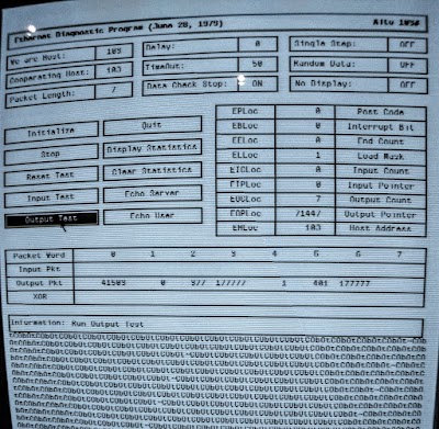
The next step was to write the PRU microcontroller code to send and receive Ethernet packets. After a lot of testing with the Alto's Ethernet Diagnostic Program (EDP), I was able to echo packets back and forth between the BeagleBone gateway and the Alto.

The Ethernet Diagnostic Program can be used to test the Ethernet. It has a simple GUI.

The Ethernet Diagnostic Program can be used to test the Ethernet. It has a simple GUI.

To be useful, the gateway must support the network stack: Pup packets, network booting, Alto-style FTP and so forth. I started by rewriting the Alto's network code, making a direct port of the BCPL implementation3 to Python. This turned out to be a mess, because the original implementation depended heavily on the Alto's operating system, which provided multiple threads, so the application could run in one thread and the network code in other threads. I managed to get the stateless low-level Pup packets to work okay, but the higher-level Byte Stream Protocol was a tangle of busy-waiting loops and timeouts.

Fortunately the Living Computers Museum+Lab (LCM+L) came to rescue. Josh Dersch at the museum had written a C# implementation of the Alto's network stack, so I decided to discard my implementation of the network stack. This implementation, called IFS,4 supported the low-level protocols, as well as servers for network operations, FTP, and Copydisk. IFS was a new implementation rather than a direct port like my attempt, and that approach worked much better.

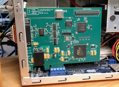
The Living Computers Museum built a 3 Mb/s Ethernet interface using an FPGA chip.

The Living Computers Museum built a 3 Mb/s Ethernet interface using an FPGA chip.

The LCM+L also built an Ethernet interface to the Alto. Theirs was much more complex than mine, consisting of an FPGA chip on a custom PCI card plugged into a PC. Unlike my interface, theirs communicated with a transceiver box, rather than connecting to the Alto directly. Even though the LCM+L's FPGA interface worked for us, I decided to complete my interface board since I liked the idea of a low-cost, compact Ethernet gateway. Their interface is more "realistic", since it connects to a real transceiver and network cable and can work with multiple Altos on a network. (The photo below shows the mini-network connecting the LCM+L interface and an Alto.) On the other hand not everyone has Ethernet transceivers lying around, so mine is more widely usable.

A very short 3 Mb/s Ethernet network, showing two transceivers attached to the coaxial cable. One transceiver is connected to the Alto and the other is connected to the LCM+L gateway card.

A very short 3 Mb/s Ethernet network, showing two transceivers attached to the coaxial cable. One transceiver is connected to the Alto and the other is connected to the LCM+L gateway card.

I made a simple printed circuit board to replace my breadboarded prototype. This was the first circuit board I had designed in about 35 years and technology has certainly changed. Back in the 1980s, I drew circuit board traces with a resist pen on a copper-clad board, and then etched the board in ferric chloride solution from Radio Shack. Now, I designed my board using Eagle, uploaded the file to OSH Park, and received a beautiful circuit board a few days later.

My 3 Mb/s Ethernet interface is a level-shifter card on a BeagleBone. Note the capacitor soldered directly to the driver IC to fix a ringing signal problem.

My 3 Mb/s Ethernet interface is a level-shifter card on a BeagleBone. Note the capacitor soldered directly to the driver IC to fix a ringing signal problem.

Running the LCM+L's IFS software on the BeagleBone took some work since the BeagleBone runs Linux and IFS was written in C# for Windows. By using the Mono platform, I could run most of the C# code on the BeagleBone. However, the LCM+L software stack communicated with the gateway by encapsulating Alto Ethernet packets in a modern Ethernet packet, using a .Net Pcap library to access the raw Ethernet. Unfortunately, this library didn't work with Mono, so I rewrote the IFS encapsulation to use UDP.

At this point the Alto and my BeagleBone implementation communicated most of the time, but there were a few tricky bugs to track down. The first problem was FTP would get sometimes bad packets. Eventually I discovered that I had mixed up byte and word counts in one place, and the large packets from FTP were overflowing the PRU's buffer.

The next problem was that when I used Copydisk to copy a disk pack from the Alto to the BeagleBone, a dropped packet caused the network to lock up after a couple minutes. This was puzzling since the sender should retransmit the lost packet after a timeout and everything should recover (like TCP). After tedious debugging, I found that if the Alto and the BeagleBone transmitted packets close together, a race condition in my code caused a dropped packet.56 Then IFS neglected to send a necessary ack when it received an unexpected packet, so the Alto kept resending the wrong packet. After fixing both my gateway code and the IFS ack, the network ran without problems.

Second version of the interface. Note the blue jumper wire to replace the missing trace.

Second version of the interface. Note the blue jumper wire to replace the missing trace.

My first version of the PCB had a few issues8 so I made a second version (above). I found that the driver chip didn't sink enough current for a long cable, so I replaced it with the chip used by the transceivers (a 7438 open collector NAND gate). I also decided to try KiCad instead of Eagle for the second board. Unfortunately, I made a mistake in KiCad7 and the new board was missing a trace, so I had to solder in a jumper (which you can seen in the photo above).

I probed the Alto's Ethernet card with an oscilloscope to check the signals it was receiving. An extender card from the LCM+L allowed us to access the card.

I probed the Alto's Ethernet card with an oscilloscope to check the signals it was receiving. An extender card from the LCM+L allowed us to access the card.

I tested the new board but it didn't work at all: the Alto wasn't receiving data or sending data. I realized that the new driver chip was a NAND gate so the signals were now inverted. I updated the PRU code to flip LOW and HIGH on the data out signal. The board still didn't work, so I probed the Alto's Ethernet board with an oscilloscope, comparing the signals from the old working board to the new failing board. Strangely, both signals were identical in the Alto and looked fine.

Eventually Marc asked me if there could be something wrong with the collision detection. I realized that the the new NAND driver was also inverting the collision detection signal. Thus, the Alto was seeing constant network collisions and refused to send or receive anything. After fixing this in my PRU software, the new board worked fine. I'm making a third revision of the board to fix the missing trace; hopefully this won't break something else.

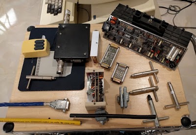
An assortment of vintage Ethernet transceivers, along with the tap tools used to drill holes in the Ethernet cable for the vampire tap connection.

An assortment of vintage Ethernet transceivers, along with the tap tools used to drill holes in the Ethernet cable for the vampire tap connection.

Conclusion

The Ethernet gateway project took much more time and encountered more problems than I expected. But it worked in the end, and several Alto owners are now using my gateway. I've open-sourced this interface (the board layout and the gateway software); it's available on github.

The Alto I've been restoring came from YCombinator; the restoration team includes Marc Verdiell, Carl Claunch and Luca Severini. My full set of Alto posts is here and Marc's extensive videos of the restoration are here. Thanks to the Living Computers Museum+Labs for the IFS software.

Follow me on Twitter or RSS to find out about my latest blog posts.

Notes and references

  1. For more information on the Pup protocol, see Pup: An Internetwork Architecture and the Pup Specifications memo.  

  2. Programming the PRU microcontrollers has a difficult learning curve, and it's not nearly as well documented as, say, the Arduino. Based on my experience with the PRU, I wrote some programming tips here and here

  3. The Alto's network code is online; you can look at one of the Pup files here. The code is written in BCPL, which was a predecssor to C. It is very similar to C, but with different syntactic choices. For instance, >> is not a shift but accesses a field in a structure. 

  4. At PARC, IFS was an acronym for Interim File System, an Alto-based distributed file server. It was called interim because an improved system was being developed, but somehow a new system never replaced IFS. 

  5. Most of the time, the BeagleBone and the Alto alternated sending packets. But every second, IFS sent a "breath of life" packet, the packet executed by the Alto to start a network boot. The breath of life packet was part of the original Alto—it simplified the network boot code since the Alto didn't need to request a network boot, but just listen for a second or two. Since the breath of life packet was asynchronous with respect to the other network traffic, eventually it would happen at a bad time for my code, triggering the dropped packet problem. 

  6. The problem with the PRU and the "breath of life" packet was due to how I was sending signals between the PRU and the main BeagleBone processor. When sending a packet, the main processor would signal the PRU, and then wait for a signal back when the packet was sent. When a packet was received, the PRU would send a signal to the main processor. The problem was that the PRU sent the same signal in both cases. So a "packet received" signal at the wrong time could wake up the packet sending code, losing the received packet. Fundamentally, I was treating the signals between the main processor and the PRU as synchronous, when everything was really asynchronous. I rewrote the gateway code so ownership of the send and receive buffers was explicitly transferred between the main processor and the PRU. A signal just indicated that ownership had changed somehow; checking the buffer status showed what exactly had changed. See this discussion for details. 

  7. My error in KiCad was I placed a net label just a bit too far from the wire on the schematic, so the wire wasn't connected to the net. 

  8. My first PCB had a couple issues that I had to hack around. Ringing in the signal to the Alto corrupted it, so I added a damping capacitor. The driver didn't have enough current for an Ethernet cable longer than 10 feet, so I added a pull-down resistor. There were also a couple mechanical issues. The location of the Ethernet jack made it hard to remove the cable, and the board blocked one of the BeagleBone buttons. I also discovered that using a 74HC125 driver chip didn't work at all; just the 74AHCT125 worked. 

An 8-tube module from a 1954 IBM mainframe examined: it's a key debouncer

IBM's vacuum tube computers of the 1950s were built from pluggable modules, each holding eight tubes and the associated components. I recently came across one of these modules so I studied its circuitry. This particular module implements five contact debouncing circuits, used to clean up input from a key or relay. When you press a key, the metal contacts tend to bounce a bit before closing, so you end up with multiple open/closed signals, rather than a nice, clean signal. The signal needs to be "debounced" to remove the extra transitions before being processed by a computer. (Perhaps you have used a cheap keyboard that sometimes gives you duplicated letters; excessive key bounce causes this.)

Front of an IBM tube module. This module contains five key debouncing circuits.

Front of an IBM tube module. This module contains five key debouncing circuits.

The module is apparently from an IBM 705, a powerful business computer introduced in 1954.1 The 705 was a big computer, weighing 16 tons. It contained 1700 vacuum tubes and consumed 70 kilowatts of power, with 40 tons2 of air conditioning to take away the heat from the tubes. A typical system cost $1,640,000 ($15 million in 2017 dollars), but was normally rented monthly for $33,500 ($300,000 in 2017 dollars). A few dozen 705 systems were built, mostly used by large companies and the US government. 8

The CPU of an IBM 705 was a massive unit. Photo from Farmers Insurance, showing their first computer.

The CPU of an IBM 705 was a massive unit. Photo from Farmers Insurance, showing their first computer.

IBM introduced multi-tube pluggable modules in 1953 as part of the 700 series of computers.3 Pluggable modules were an innovation that simplified manufacturing and maintenance, as well as providing a way to pack circuitry densely. Computers were built from hundreds of pluggable modules of many different types. The photo below shows how the 8-tube modules were packed in the IBM 709.

Closeup of tube modules in the IBM 709. Note that the modules are installed "sideways" with the tubes horizontal.

Closeup of tube modules in the IBM 709. Note that the modules are installed "sideways" with the tubes horizontal.

IBM hoped that they could manufacture a small set of common pluggable modules, but this didn't work out since the computers required many different types of modules. Instead, IBM settled for modules that were built from standardized design rules and circuits. The main circuit classes were the inverter, the flip flop (which IBM called a "trigger"), diode logic,6 the multivibrator (pulse generator), and the cathode follower (buffer).75 Unfortunately even this level of standardization didn't work too well. For instance, they ended up with dozens of different types of inverters for special cases, everything from an "Open-filament neon inverter" to a "Line capacity yanker". Thus, each computer ended up with hundreds of different types of tube modules, built from a multitude of circuits.4

A single tube module could contain a couple dozen of these simple circuits. You might wonder how eight tubes could support so many circuits, but there were two factors. First, the tubes were typically dual triodes in one package, so the module had the equivalent of 16 simple tubes. Also, AND and OR logic gates were implemented in the module with compact semiconductor diodes, so complex Boolean logic could be implemented almost for free.

I've seen claims that an 8-tube module represents an 8-bit byte, but that's not the case. The eight tubes don't generally map onto eight of anything since functions can take more or less than one tube. For instance, the module I examined contains five circuits. I have another module that stored three bits. Also, the byte wasn't a thing back then. These computers used 36-bit words (scientific models), or 6-bit characters (business models) so 8 bits was irrelevant.

Vacuum tubes

This module was built from a type of vacuum tube known as a triode. In a triode, electrons flow from the cathode to the plate (or anode), under the control of the grid. The heater, similar to a light bulb filament, heats the cathode to around 1000°F, causing electrons to "boil" off the cathode. The anode has a large positive voltage (e.g. +140V), which attracts the negatively-charged electrons. The grid is placed between the cathode and the anode. If the grid is negative, it repels the electrons, blocking the flow to the plate. Thus, the triode can act as a switch, with the grid turning on and off the flow of electrons. The module I examined used dual triode tubes, combining two triodes into one tube for compactness. 9

Schematic symbol for a triode tube

Schematic symbol for a triode tube

Vacuum tubes required inconveniently large voltages; this module used -130V. -60V, +140V and 6.3VAC. Tubes also had high power consumption—note the many large (1 watt) resistors in the module. The filament was hot enough to glow, using a couple watts per tube. In total, each tube module probably used dozens of watts of power.

A 5965 vacuum tube from the module. The pins plug into a socket on top of the tube module. This tube is a dual-triode; the two plate structures are visible.

A 5965 vacuum tube from the module. The pins plug into a socket on top of the tube module. This tube is a dual-triode; the two plate structures are visible.

The module's circuitry

I closely examined the tube module and found that it consisted of five copies of the same circuit. I traced out one of these circuits, which was a bit inconvenient because the module has components on both the front and the back. I came across a manual of 700-series circuits, and found a circuit that was an exact match, down to the values of the resistors. The circuit is called a "Contact-Operated Trigger" and was used to interface a mechanical input (key, relay, or cam) to electronic circuits.1

Schematic of one "trigger" circuit of the tube module.

Schematic of one "trigger" circuit of the tube module.

The schematic above shows one of the trigger stages. The basic idea of this circuit is a resistor-capacitor filter (left) smooths out the input, removing any short glitches. This signal goes through two inverter circuits, creating a sharp output. Both inverters are part of the same 6211 tube and are wired as a Schmitt trigger.12 To understand how the inverter works, when the input (pin 2) is high, the current through the tube pulls the plate (pin 1) low. Conversely, when the input is low, the electron flow is blocked and the resistors pull the plate high.10 The output from the first inverter (plate, pin 1) is fed into the second inverter (grid, pin 7). This inverter works similarly, with its output on pin 6. The final output is buffered by a "cathode follower" circuit (not shown) to drive other modules. It also drives a neon bulb for a status indicator,

The tube module showing how the five debounce triggers are divided among the tubes.

The tube module showing how the five debounce triggers are divided among the tubes.

The tube module contains five of the above debounce circuits. The diagram above shows how these circuits map onto the eight tubes. Each cathode follower (CF) uses half a tube so one tube implements two cathode followers.11

One amusing component I found in the tube module was "Vitamin Q" capacitors. Presumably this is related to the quality factor or Q factor in radio, and these capacitors were designed to improve the Q.

A Vitamin Q capacitor in an IBM 705 tube module.

A Vitamin Q capacitor in an IBM 705 tube module.

A brief history of vacuum tube computing, with a focus on IBM

It took longer to get from the invention of the vacuum tube to the development of electronic computer than you might expect. The triode vacuum tube was invented in 1907 and started being used for radio in 1912. The vacuum tube flip-flop, able to store one bit of data was invented by Eccles and Jordan in 1918, but it wasn't until about 1937 that flip flops were connected together into binary counters.

IBM started investigating vacuum tube counters for calculations in 1941 and built an experimental vacuum tube multiplier in 1942. In 1948, IBM introduced the IBM 604 "Electronic Calculating Punch", which implemented high-speed arithmetic operations for punch-card systems by using vacuum tubes. It was IBM's first product with pluggable tube units, using simple modules with one or two vacuum tubes in each module (as seen below).14

Two tube modules from the IBM 604. By Jud McCranie CC BY-SA 4.0, via Wikimedia Commons

Two tube modules from the IBM 604. By Jud McCranie CC BY-SA 4.0, via Wikimedia Commons

Meanwhile, vacuum tube computers were being invented, with Atanasoff's linear equation solver built in 1942 and the Colossus codebreaking system in 1943. But it wasn't until the programmable ENIAC computer was announced in 1946 that the vacuum tube computer revolution really started, leading to the development of numerous computers by the early 1950s.

In 1952, announced the 701, IBM's first commercial scientific computer. The 701 introduced multi-tube pluggable modules, the focus of this article. These modules were used in the 700-series computers until they were obsoleted in 1958 by IBM's transistorized 7000-series computers, which used germanium transistors. The transistorized computers were built from printed circuit boards the size of a playing card, called SMS cards.13 Thus, although vacuum tube computers were highly influential, their lifespan was short. (Transistorized computers also had a short lifespan of a bit over a decade. Integrated circuits, on the other hand, have been powering computers for more than 50 years, with no signs of being replaced.)

A tube module implements more logic than an SMS card, but the cards are much smaller and use less power. Photo shows a "DGT" SMS card implementing four AND gates on top of a different tube module.

A tube module implements more logic than an SMS card, but the cards are much smaller and use less power. Photo shows a "DGT" SMS card implementing four AND gates on top of a different tube module.

How the modules are built

One important advantage of the tube module is the circuitry is somewhat three-dimensional, compared to components soldered on a circuit board. This allows the circuitry to more efficiently fill the volume of the computer. The module has four layers of contact boards with terminal strips attached, allowing four vertical layers of components (resistors, capacitors, etc) to be soldered to the terminal strips.5 The solder terminals are connected together by thin horizontal metal strips, which can be cut. Thus, neighboring tabs can be electrically connected or not, as required by the circuit. Jumper wires are used to provide additional connections as needed.

The module has four levels of components between the tubes and the connector. In addition, there are components on the front and back of the module.

The module has four levels of components between the tubes and the connector. In addition, there are components on the front and back of the module.

The tube module has 64 metal contact tabs at the bottom, providing connections for power and signals. The tube module doesn't simply plug into the socket as you might expect, but uses a two step mechanism. First, the module is placed in the socket but the pins don't make contact. You may have noticed the rod sticking up from the top of the module. To lock the module into place, the rod is rotated 180 degrees with a special tool, causing a circular cam at the bottom of the module to rotate. The force of the cam against the socket causes the module to slide sideways so the pins mesh with the socket contacts. This reduces the force required to insert the module and minimizes the risk of the module coming loose.

The module has 64 metal tabs that plug into the socket. The circular cam (rusted) rotates to slide the module (and the tabs) sideways into the socket.

The module has 64 metal tabs that plug into the socket. The circular cam (rusted) rotates to slide the module (and the tabs) sideways into the socket.

The contacts are carefully positioned to establish the ground connection first, then the negative-voltage connections and finally the positive connections. This allows hot-swapping, replacing a tube module while the system is powered up. (The manual does say, "However, it is wise to drop DC voltages before removing or installing pluggable units.") Interestingly, USB connectors use the same idea. If you look at a USB connector, you'll see that the middle two contacts (data) are shorter than the outside contacts (power and ground), so power and ground connections are established first.

Patent 2,754,454 describes the tube module mechanism in detail.

Patent 2,754,454 describes the tube module mechanism in detail.

The tube module has locking tabs that holds the module into place after it slides sideways. I noticed that these tabs are broken off on the module I examined; compare with the intact module below. Probably the rusted cam couldn't be moved, so the module had to be forced out of the socket, breaking the tabs.

When the tube module slides sideways into the connectors, the locking tabs engage to keep it from being pulled out. In this tube module, the locking tabs are broken off.

When the tube module slides sideways into the connectors, the locking tabs engage to keep it from being pulled out. In this tube module, the locking tabs are broken off.

More evidence of the module's hard life is there are at least four resistors missing from the module, and two resistors with broken solder joints. (This made it considerably harder to figure out what the module did.) Positions where two components are soldered to the same tabs seem especially prone to having a component knocked off. The photo below illustrates one of the missing resistors; one trigger circuit has a 91K (white-brown-orange) resistor soldered across the capacitor, while it is missing in the second circuit.

The arrow shows one of the missing resistors in the tube module.

The arrow shows one of the missing resistors in the tube module.

Conclusion

The tube module is an interesting artifact from the era of vacuum tube computers. Studying it revealed its function, five contact debouncing circuits for use with keys or relays. Part II of this blog post will describe powering up the module and getting it to work. For a sneak preview, you can watch CuriousMarc's video:

Thanks to Carl Claunch for providing the module.

Follow me on Twitter or RSS to find out about my latest blog posts.

Notes and references

  1. I found the circuit for this module in a manual of circuits for IBM's 700-series computers (page C35). Chapter C has information on circuits for the 702 and 705 business systems (which use different voltages from the scientific 701, 704 and 709 systems described in chapter B). Since the 705 was much more popular than the 702, it's more likely that the module is from a 705. 

  2. Strangely, a ton of refrigeration means cooling equal to one ton of ice per day, not an air conditioner that weights one ton. This unit probably made more sense in the 1900s when people were switching from ice-based cooling to refrigeration. In more sensible units, one ton of refrigeration is 12,000 BTU/hour or about 3500 Watts. For comparison, a typical window air conditioner is one ton of cooling, while a central home air conditioner is 1.5 to 5 tons of cooling. 

  3. Several detailed articles on the IBM 701 computer, written by the designers in 1953 are here.  

  4. IBM went through a similar failed standardization process in the 1960s with their transistorized Standard Modular System (SMS) cards. They hoped to build computers from a small number of standard cards but ended up with thousands of different cards

  5. IBM's 700 Series Data Processing System Component Circuits provides extremely detailed information on the circuits used in tube modules. If you want to know all about tube modules, this is the document to read. A couple other pages of interest are the IBM 709 CPU Diagrams with schematics of the 709's tube modules and IBM 705 Drawings with a few 705 tube modules. The 1952 patent, Multiple Pluggable Unit, describes the mechanical structure of the tube modules in detail. A few drawings of 705 circuits are here, and 709 drawings are here. Bitsavers has some information on the 704 including details of the circuitry, but not to the tube level. Bitsavers' information on the 701, 702, 705 and 709 is less relevant. 

  6. The development of the semiconductor diode significantly reduced the size of computers, as small diodes could perform logic functions (AND, OR) that previously required vacuum tubes. The IBM 706 contained many more diodes than vacuum tubes: 4600 germanium diodes versus 1700 vacuum tubes. I think the importance of diodes is underestimated, with people focusing on tubes versus transistors. 

  7. The tube modules are described in more detail in the book IBM's Early Computers, pages 147-151. 

  8. The BRL Report has details on most computer systems as of 1961, including the 705. Take a look at this report if you want to know the size, price, features, or number of components in old computers. 

  9. The module uses two types of vacuum tubes: five 6211 tubes and three 5965 tubes. Both tubes were designed for computer applications, able to handle the stress of constantly turning signals on and off (unlike radio applications, where tubes handled analog signals). They are both dual triodes, but the 5965 is a higher power tube. The 5965 tube is IBM number 317261. The 6211 tube is IBM number 252551. The 5965 tube handles up to 300V, while the 6211 only 200V. The 5965 also handles more current and has higher gain, which is probably why it is used in the cathode follower driver circuit. For full details on the tubes, see the 5965 datasheet and the 6211 datasheet. These tubes are both similar to the more common 12AT7 tube

  10. The various resistors adjust (biasing) the voltage levels from the high plate voltage to the lower voltages used by the grid. (That's why the -130V supply is needed, to pull the voltage down enough.) 

  11. The triggers are implemented with type 6211 tubes, while the cathode followers are implemented with the more powerful 5965 tubes. From the photo, it may appear that the tubes don't match the locations since there are four tubes with metallized tops and four tubes with metallized sides. However, the tube markings indicate that all tubes were in the right locations. The location of the shiny getter is independent of the tube type. 

  12. The tube is wired as a Schmitt trigger. When the input becomes sufficiently high, it will rapidly switch to the on state. The input will need to fall to a lower level, at which point it will rapidly switch to the off state. The key to the Schmitt trigger is the resistor connected to the cathodes. When one tube turns on, the voltage drop across the resistor will raise the the cathode voltage close to the grid voltage. This will force the other tube off. You can also look at it as a differential amplifier, where the higher grid "wins". 

  13. If you want a quick summary of IBM's machines from the 701 through the 370, see The Architecture of IBM's Early Computers and "System/360 and Beyond". 

  14. The book IBM's Early Computers has extremely detailed information on IBM's pre-360 machines. Also see IBM's web page on the 603