Inside Intel's first product: the 3101 RAM chip held just 64 bits

Intel's first product was not a processor, but a memory chip: the 31011 RAM chip, released in April 1969. This chip held just 64 bits of data (equivalent to 8 letters or 16 digits) and had the steep price tag of $99.50.2 The chip's capacity was way too small to replace core memory, the dominant storage technology at the time, which stored bits in tiny magnetized ferrite cores. However, the 3101 performed at high speed due to its special Schottky transistors, making it useful in minicomputers where CPU registers required fast storage. The overthrow of core memory would require a different technology—MOS DRAM chips—and the 3101 remained in use in the 1980s.3

This article looks inside the 3101 chip and explains how it works. I received two 3101 chips from Evan Wasserman and used a microscope to take photos of the tiny silicon die inside.4 Around the outside of the die, sixteen black bond wires connect pads on the die to the chip's external pins. The die itself consists of silicon circuitry connected by a metal layer on top, which appears golden in the photo. The thick metal lines through the middle of the chip power the chip. The silicon circuitry has a grayish-purple color, but it largely covered by the metal layer. Most of the chip contains a repeated pattern: this is the 16x4 array of storage cells. In the upper left corner of the chip, the digits "3101" in metal identify the chip, but "Intel" is not to be found.

Die photo of the Intel 3101 64-bit RAM chip. Click for a larger image.

Die photo of the Intel 3101 64-bit RAM chip. Click for a larger image.

Overview of the chip

The 3101 chip is controlled through its 16 external pins. To select one of the chip's 16 words of memory, the address in binary is fed into the chip through the four address pins (A0 to A3). Memory is written by providing the 4-bit value on the data input pins (D1 to D4). Four data output pins (O1 to O4) are used to read memory; these pins are inverted as indicated by the overbar. The chip has two control inputs. The chip select pin (CS) enables or disables the chip. The write enable pin (WE) selects between reading or writing the memory. The chip is powered with 5 volts across the Vcc and ground pins.

The diagram below shows how the key components of the 3101 are arranged on the die. The RAM storage cells are arranged as 16 rows of 4 bits. Each row stores a word, with bits D1 and D2 on the left and D3 and D4 on the right. The address decode logic in the middle selects which row of storage is active, based on the address signals coming from the address drivers at the top. At the bottom, the read/write drivers provide the interface between the storage cells and the data in and out pins.

Block diagram of the 3101 RAM chip.

Block diagram of the 3101 RAM chip.

Transistors

Transistors are the key components in a chip. The 3101 uses NPN bipolar transistors, different from the MOS transistors used in modern memory chips. The diagram below shows one of the transistors in the 3101 as it appears on the die. The slightly different tints in the silicon indicate regions that have been doped to form N and P type silicon with different semiconductor properties. The cross-section diagram illustrates the internal structure of the transistor. On top (black) are the metal contacts for the collector (C), emitter (E), and base (B). Underneath, the silicon has been doped to form the N and P regions that make up the transistor.

A key innovation of the 3101 was using Schottky transistors (details), which made the 3101 almost twice as fast as other memory chips.5 In the cross section, note that the base's metal contact touches both the P and N regions. You might think this shorts the two regions together, but instead a Schottky diode is formed where the metal contacts the N layer.6

The structure of an NPN Schottky transistor inside the Intel 3101 chip.

The structure of an NPN Schottky transistor inside the Intel 3101 chip.

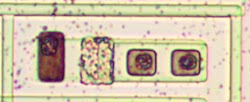
The 3101 also used many multiple-emitter transistors. While a multiple-emitter transistors may seem strange, they are common in bipolar integrated circuits, especially TTL logic chips. A multiple-emitter transistor simply has several emitter regions embedded in the base region. The die photo below shows one of these transistors with the collector on the left, followed by the base and two emitters.

A multiple-emitter transistor from the Intel 3101 chip.

A multiple-emitter transistor from the Intel 3101 chip.

Driving the data output pins requires larger, high-current transistors. The image below shows one of these transistors. The central rectangle is the base, surrounded by the C-shaped emitter in the middle and the large collector on the outside. Eight of these high-current transistors are also used to drive the internal address select lines.

For the high-current output, the Intel 3101 chip uses larger transistors.

For the high-current output, the Intel 3101 chip uses larger transistors.

Diodes

While examining the 3101 chip, I was surprised by the large number of diodes on the chip. Eventually I figured out that the chip used DTL (diode-transistor logic) for most of its logic rather than TTL (transistor-transistor logic) that I was expecting. The diagram below shows one of the diodes on the chip. I believe the chip builds diodes using the standard technique of connecting an NPN transistor as a diode.

Presumed structure of a diode inside the 3101 chip. I believe this is a regular diode, not a Schottky diode.

Presumed structure of a diode inside the 3101 chip. I believe this is a regular diode, not a Schottky diode.

Resistors

The die photo below shows several resistors on the 3101 die. The long, narrow snaking regions of p-type silicon provide resistance. Resistors in integrated circuits are inconveniently large, but are heavily used in the 3101 for pull-up and pull-down resistors. At the right is a square resistor, which has low resistance because it is very wide.7 It is used to route a signal under the metal layer, rather than functioning a resistor per se.

Resistors inside the 3101 chip.

Resistors inside the 3101 chip.

The static RAM cell

Now that I've explained the individual components of the chip, I'll explain how the circuitry is wired together for storage. The diagram below shows the cell for one bit of storage with the circuit diagram overlaid. Each cell consists of two multi-emitter transistors (outlined in red) and two resistors (at the top). The horizontal and vertical wiring connects cells together. This circuit forms a static RAM cell, basically a latch that can be in one of two states, storing one data bit.

The circuitry of one storage cell of the 3101 RAM chip. The two multiple-emitter transistors are outlined in red.

The circuitry of one storage cell of the 3101 RAM chip. The two multiple-emitter transistors are outlined in red.

Before explaining how this storage cell works, I'll explain a simpler latch circuit, below. This circuit has two transistors cross-connected so if one transistor is on, it forces the other off. In the diagram, the left transistor is on, which keeps the right transistor off, which keeps the left transistor on. Thus, the circuit will remain in this stable configuration. The opposite state—with the left transistor off and the right transistor on—is also stable. Thus, the latch has two stable configurations, allowing it to hold a 0 or a 1.

A simple latch circuit. The transistor on the left is on, forcing the transistor on the right off, forcing the transistor on the left off...

A simple latch circuit. The transistor on the left is on, forcing the transistor on the right off, forcing the transistor on the left off...

To make this circuit usable—so the bit can be read or modified—more complex transistors with two emitters are used. One emitter is used to select which cell to read or write, while the other emitter is used for the read or write data. This yields the schematic below, which matches the storage cell die photo diagram above.

The RAM cell used in the Intel 3101 is based on multiple-emitter transistors. The row select lines are raised to read/write the row of cells. Each data line accesses a column of cells.

The RAM cell used in the Intel 3101 is based on multiple-emitter transistors. The row select lines are raised to read/write the row of cells. Each data line accesses a column of cells.

Multiple storage cells are combined into a grid to form the memory memory. One word of memory consists of cells in the same row that share select lines. All the cells in a column store the same bit position; their data lines are tied together. (The bias line provides a voltage level to all cells in the memory.8)

Note that unlike the simplified cell, the circuit above doesn't have an explicit ground connection; to be powered, it requires a low input on either the select or data/bias lines. There are three cases of interest:

  • Unselected: If the negative row select line is low, current flows out through the row select line. The data and bias lines are unaffected by this cell.
  • Read: If the negative row select line is higher than the data and bias lines, current will flow out the data line if the left transistor is on, and out the bias line if the right transistor is on. Thus, the state of the cell can be read by examining the current on the data line.
  • Write: If the negative row select line is higher and the data and bias lines have significantly different voltages, the transistor on the lower side will switch on, forcing the cell into a particular state. This allows a 0 or 1 to be written to the cell.

Thus, by carefully manipulating the voltages on the select lines, data lines and the bias line, one row of memory can be read or written, while the other cells hold their current value without influencing the data line. The storage cell and the associated read/write circuitry are essentially analog circuits rather than digital since the select, data, and bias voltages must be carefully controlled voltages rather than logic levels.

The address decode logic

The address decode circuitry determines which row of memory cells is selected by the address lines.11 The interesting thing about this circuitry is that you can easily see how it works just by looking at the die photo. The address driver circuitry sends the four address signals along with their complements on eight metal traces through the chip. Each storage row has a four-emitter transistor. In each row you can see four black dots, which are the connections between emitters and address lines. A row will be selected if all the emitter inputs are high.9 A dot on an address line (e.g. A0) will "match" a 1, while a dot on the complemented address line (e.g. A0) will match a 0, so each row matches a unique four-bit address. In the die photo below, you can see the decoding logic counting down in binary for rows 15 down to 11;10 the remainder of the circuit follows the same pattern.

The address decode logic in the Intel 3101 RAM chip. Each row decodes matches four address lines to decode one of the 16 address combinations. You can see the value counting down in binary.

The address decode logic in the Intel 3101 RAM chip. Each row decodes matches four address lines to decode one of the 16 address combinations. You can see the value counting down in binary.

Some systems that used the 3101

The 64-bit storage capacity of the 3101 was too small for a system's main memory, but the chip had a role in many minicomputers. For example, the Burroughs D Machine was a military computer (and the source of the chips I examined). It used core memory for its main storage, but a board full of 3101 chips provided high-speed storage for its microcode. The Xerox Alto used four 3101 chips to provide 16 high-speed registers for the CPU, while the main memory used slower DRAM chips. Interdata used 3101 chips in many of its 16- and 32-bit minicomputers up until the 1980s.12

The 3101 was also used in smaller systems. The Diablo 8233 terminal used them as RAM.13 The Datapoint 2200 was a "programmable terminal" that held its processor stack in fast 3101 chips rather than the slow main memory which was built from Intel 1405 shift registers.

The CPU of the Datapoint 2200 computer was built from a board full of TTL chips. The four white chips in the lower center-right are Intel 3101 RAM chips holding the stack. Photo courtesy of Austin Roche (I think).

The CPU of the Datapoint 2200 computer was built from a board full of TTL chips. The four white chips in the lower center-right are Intel 3101 RAM chips holding the stack. Photo courtesy of Austin Roche (I think).

How I created the die photos

To get the die photos, I started with two chips that I received thanks to Evan Wasserman and John Culver. The pins on the chips had been crushed in the mail, but this didn't affect the die photos. The chips had two different lot numbers that indicate they were manufactured a few months apart. Strangely, the metal lids on the chips were different sizes and the dies were slightly different. For more information, see the CPU Shack writeup of the 3101.

Two 3101 RAM chips. The chip on the right was manufactured slightly later and has a larger lid over the die.

Two 3101 RAM chips. The chip on the right was manufactured slightly later and has a larger lid over the die.

Popping the metal lid off the chips was easy—just a tap with a hammer and chisel. This revealed the die inside.

With the lid removed, you can see the die of the 3101 RAM chip and the bond wires connected to the die.

With the lid removed, you can see the die of the 3101 RAM chip and the bond wires connected to the die.

Using a metallurgical microscope and Hugin stitching software (details), I stitched together multiple microscope photos to create an image of the die. The metal layer is clearly visible, but it obscures the silicon underneath, making it hard to determine the chip's circuitry. The photo below shows a closeup of the die showing the "3101" part number.

The die photo of the Intel 3101 shows mostly the metal layer.

The die photo of the Intel 3101 shows mostly the metal layer.

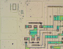
I applied acid14 to remove the metal layer. This removed most of the metal, revealing the silicon circuitry underneath. Some of the metal is still visible, but thinner, appearing transparent green. Strangely, the number 3101 turned into 101; apparently the first digit wasn't as protected by oxide as the other digits.

Treatment with acid dissolved most of the metal layer of the 3101 chip, revealing the silicon circuits underneath.

Treatment with acid dissolved most of the metal layer of the 3101 chip, revealing the silicon circuits underneath.

Below is the complete die photo of the chip with the metal layer partially stripped off. (Click it for a larger version.) This die photo was most useful for analyzing the chip. Enough of the metal was removed to clearly show the silicon circuits, but the remaining traces of metal showed most of the wiring. The N+ silicon regions appear to have darkened in this etch cycle.

Die photo of the Intel 3101 64-bit RAM chip with metal layer partially stripped off.

Die photo of the Intel 3101 64-bit RAM chip with metal layer partially stripped off.

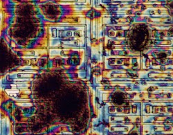
I wanted to see how the chip looked with the metal entirely removed so I did a second etch cycle. Unfortunately, this left the die looking like it had been destroyed.

After dissolving most of the oxide layer, the die looks like a mess. (This is a different region from the other photos.)

After dissolving most of the oxide layer, the die looks like a mess. (This is a different region from the other photos.)

I performed a third etch cycle. It turns out that the previous etch hadn't destroyed the die, but just left a thin layer of oxide that caused colored interference bands. The final etch removed the remaining oxide, leaving a nice, clean die. Only a ghost of the "101" number is visible. The contacts between the metal layer and the silicon remained after the etch; they may be different type of metal that didn't dissolve.

The metal and oxide have been completely removed from the 3101 die, showing the silicon layer.

The metal and oxide have been completely removed from the 3101 die, showing the silicon layer.

Below is the full die photo with all the metal stripped off. (Click it for a full-size image.)

Die photo of the Intel 3101 64-bit RAM chip with metal layer stripped off.

Die photo of the Intel 3101 64-bit RAM chip with metal layer stripped off.

Conclusion

The 3101 RAM chip illustrates the amazing improvements in integrated circuits driven by Moore's Law.15 While the 3101 originally cost $99.50 for 64 bits, you can now buy 16 gigabytes of RAM for that price, two billion times as much storage. If you built a 16 GB memory from two billion 3101 chips, the chips alone would weigh about 3000 tons and use over a billion watts, half of Hoover Dam's power. A modern 16GB DRAM module, in comparison, uses only about 5 watts.

As for Intel, the 3101 RAM was soon followed by many other memory products with rapidly increasing capacity, making Intel primarily a memory company that also produced processors. However, facing strong competition from Japanese memory manufacturers, Intel changed its focus to microprocessors and abandoned the DRAM business in 1985.16 By 1992, the success of the x86 processor line had made Intel the largest chip maker, justifying this decision. Even though Intel is now viewed as a processor company, it was the humble 3101 memory chip that gave Intel its start.

Thanks to Evan Wasserman and John Culver for sending me the chips. John also did a writeup of the 3101 chip, which you can read at CPU Shack.

Notes and references

  1. You might wonder why Intel's first chip had the seemingly-arbitrary number 3101. Intel had a highly-structured naming system. A 3xxx part number indicated a bipolar product. A 1 for the second digit indicated RAM, while the last two digits (01) were a sequence number. Fortunately, the marketing department stepped in and gave the 4004 and 8008 processors better names. 

  2. Memory chips started out very expensive, but prices rapidly dropped. Computer Design Volume 9 page 28, 1970, announced a price drop of the 3101 from $99.50 to $40 in small volumes. Ironically, the Intel 3101 is now a collector's item and on eBay costs much more than the original price—hundreds of dollars for the right package. 

  3. Several sources say that the 3101 was the first solid state memory, but this isn't accurate. There were many companies making memory chips in the 1960s. For instance, Texas Instruments announced the 16-bit SN5481 bipolar memory chip in 1966 (Electronics, V39 #1, p151) and Transitron had the TMC 3162 and 3164 16-bit RAM (Electrical Design News, Volume 11, p14). In 1968, RCA made 72-bit and 288-bit CMOS memories for the Air Force (document, photo). Lee Boysel built 256-bit dynamic RAMs at Fairchild in 1968 and 1K dynamic RAMs at Four Phase Systems in 1969 (timeline and Boysel presentation). For more information on the history of memory technology, see timeline and History of Semiconductor Engineering, p215. Another source for memory history is To the Digital Age, p193. 

  4. From my measurements, the 3101 die is about 2.39mm by 3.65mm. Feature size is about 12µm. 

  5. If you've used TTL chips, you probably used the 74LSxx family. The "S" stands for the Schottky transistors that make these chip fast. These chips were "the single most profitable product line in the history of Texas Instruments" (ref). 

  6. The Schottky diode in the Schottky transistor is formed between the base and collector. This diode prevents the transistor from becoming saturated, allowing it to switch faster. 

  7. The resistance of an IC resistor is proportional to the length divided by the width. The sheet resistance of a material is measured in the unusual unit of ohms per square. You might think it should be per square nanometer or square mm or something, but since the resistance depends on the ratio of length to width, the unit cancels out. 

  8. The bias line is shared by all the cells. For reading, it is set to a low voltage. For writing, it is set to an intermediate voltage: higher than the data 0 voltage, but lower than the data 1 voltage. The bias voltage is controlled by the write enable pin.

    More advanced chips use two data lines instead of a bias line for more sensitivity. A differential amplifier to compare the currents on the two data lines and distinguish the tiny change between a zero bit and a one bit. However, the 3101 uses such high currents internally that this isn't necessary; it can read the data line directly. 

  9. If my analysis is correct, when a row is selected, the address decode logic raises both the positive row select and negative row select lines by about 0.8 volts (one diode drop). Thus, the cell is still powered by the same voltage differential, but the voltage shift makes the data and bias lines active. 

  10. Address lines A3 and A2 are reversed in the decoding logic, presumably because it made chip layout simpler. This has no effect on the operation of the chip since it doesn't matter of the physical word order matches the binary order. 

  11. The 3101 has a chip select pin that makes it easy to combine multiple chips into a larger memory. If this pin is high, the chip will not read or write its contents. One strange thing about the address decoding logic is that each pair of address lines is driven by a NAND gate latch. There's no actual latching happening, so I don't understand why this circuit is used.

    How the 3101 implements this feature is a bit surprising. The chip select signal is fed into the address decoding circuit; if the chip is not selected, both A0 and the complement A0 are forced low. Thus, none of the rows will match in the address decoding logic and the chip doesn't respond. 

  12. The Interdata 7/32 (the first 32-bit minicomputer) used 3101 chips in its memory controller. (See the maintenance manual page 338.) The Interdata 16/HSALU used 3101 chips for its CPU registers. (See the maintenance manual page 259.) As late as 1982, the Interdata 3210 used 3101 chips to hold cache tags (see manual page 456). On the schematics note that part number 19-075 indicates the 3101. 

  13. The Diablo 8233 terminal used 3101A (74S289) chips as RAM for its discrete TTL-based processor (which was more of a microcontroller) that controlled the printer. (See maintenance manual page 187.) This systems was unusual since it contained both an 8080 microprocessor and a TTL-based processor. 

  14. The metal layer of the chip is protected by silicon dioxide passivation layer. The professional way to remove this layer is with dangerous hydrofluoric acid. Instead, I used Armour Etch glass etching cream, which is slightly safer and can be obtained at craft stores. I applied the etching cream to the die and wiped it for four minutes with a Q-tip. (Since the cream is designed for frosting glass, it only etches in spots. It must be moved around to obtain a uniform etch.) Next, I applied a few drops of hydrochloric acid (pool acid from the hardware store) to the die for a few hours. 

  15. Moore's law not only describes the exponential growth in transistors per chip, but drives this growth. The semiconductor industry sets its roadmap according to Moore's law, making it in some sense a self-fulfilling prophecy. See chapter 8 of Technological Innovation in the Semiconductor Industry for a thorough discussion. 

  16. Intel's 1985 Annual Report says "It was a miserable year for Intel" and discusses the decision to leave the DRAM business. 

Bitcoin mining on a vintage Xerox Alto: very slow at 1.5 hashes/second

I've been restoring a Xerox Alto minicomputer from the 1970s and figured it would be interesting to see if it could mine bitcoins. I coded up the necessary hash algorithm in BCPL (the old programming language used by the Alto) and found that although the mining algorithm ran, the Alto was so slow that it would take many times the lifetime of the universe to successfully mine bitcoins.

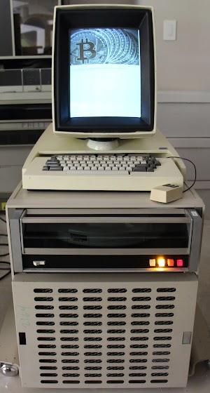
Bitcoin mining on a vintage Xerox Alto computer.

Bitcoin mining on a vintage Xerox Alto computer.

The Alto was a revolutionary computer designed at Xerox PARC in 1973 to investigate personal computing. It introduced high-resolution bitmapped displays, the GUI, Ethernet and laser printers to the world, among other things. In the photo above, the Alto computer is in the lower cabinet. The black box is the 2.5 megabyte disk drive. The Alto's unusual portrait display and an early optical mouse are on top.

How Bitcoin mining works

Bitcoin, a digital currency that can be transmitted across the Internet, has attracted a lot of attention lately. The Bitcoin system can be thought of as a ledger that keeps track of who owns which bitcoins, and allows them to be transferred from one person to another. The revolutionary feature of Bitcoin is there's no central machine or authority keeping track of things. Instead, the "blockchain" is stored across thousands of machines on the Internet, and the system works with nobody in charge.

To ensure everyone agrees on which transactions are valid, Bitcoin uses a process called mining—about every 10 minutes a block of outstanding transactions is mined, which makes the block "official". Bitcoin mining is designed to take an insanely huge amount of computational effort to mine a block, so nobody can take over the mining process. Miners compete against each other, generating trillions and trillions of "hashes" until someone finds a lucky one that succeeds in mining a block. It's hard to visualize just how difficult the hashing process is: finding a valid hash is less likely than finding a single grain of sand out of all the sand on Earth.

Bitcoin mining is based on cryptography, with a "hash function" that converts a block into an essentially random hash value. If the hash starts with 17 zeros,1 the block is successfully mined and is sent into the Bitcoin network. Most of the time the hash isn't successful, so the miner will modify the block slightly and try again, over and over billions of times. About every 10 minutes someone will successfully mine a block, and the process starts over. It's kind of like a lottery, where miners keep trying until someone "wins".

As a side-effect, mining adds new bitcoins to the system. For each block mined, miners currently get 12.5 new bitcoins (currently worth about $30,000) as well as fees, which encourages miners to do the hard work of mining blocks. With the possibility of receiving $30,000 every 10 minutes, miners invest in datacenters full of specialized mining hardware using huge amounts of electricity2.

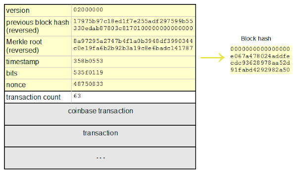
Structure of a Bitcoin block

Structure of a Bitcoin block. The data in yellow is hashed to yield the block hash, which becomes the identifier for the block. The block is linked to the previous block by including the previous block's hash, forming the blockchain. The Merkle root is a hash of all the transactions in the block.

The diagram above shows what actually goes into a block that is mined. The yellow part is the block header (which gets hashed), and it is followed by the transactions that go into the block. Each block contains the hash of the previous block, causing all the blocks to be linked together forming the blockchain. You can see that for the block above, the hash is successful because it starts with lots of zeros: 0000000000000000e067a478024addfecdc93628978aa52d91fabd4292982a50. The "Merkle root" is a hash of all the transactions that go into the block; this ensures that none of the mined transactions can be changed. The nonce is an arbitrary number; each attempt at mining the block changes the nonce.

To summarize the mining process: you collect new Bitcoin transactions and create a header (as in the diagram above). You do the cryptographic hash of the block. If by some incredible chance the result starts with 17 zeros you send the block into the Bitcoin network and "win" $30,000 in bitcoin. Otherwise, you change the nonce and try again. Probably none of the nonce values will work, so you change something else in the header and start over. If someone else succeeds in mining the block, you start over with the new previous block hash and new transactions.

I've simplified a lot of details above. For in-depth information on Bitcoin and mining, see my articles Bitcoins the hard way and Bitcoin mining the hard way.

The SHA-256 hash algorithm used by Bitcoin

Next, I'll discuss the hash function used in Bitcoin, which is based on a standard cryptographic hash function called SHA-256.3 The SHA-256 algorithm is so simple you can literally do it by hand, but it manages to scramble the data entirely unpredictably. The SHA-256 hash algorithm takes input blocks of 512 bits (i.e. 64 bytes), combines the data cryptographically, and generates a 256-bit (32 byte) output.

The SHA-256 algorithm consists of a simple round repeated 64 times. The diagram below shows one round, which takes eight 4-byte inputs, A through H, performs a few operations, and generates new values for A through H. As can be seen from the diagram above, only A and E are changed in a round, while the others are just shifted over. Even so, after 64 rounds the input data will be completely scrambled, generating the unpredictable hash output.

The SHA-256 algorithm is pretty simple, about a page of pseudocode and can be easily implemented on a computer, even one as old as the Alto, using simple arithmetic and logic operations.5

SHA-256 round, from Wikipedia

SHA-256 round, from Wikipedia created by kockmeyer, CC BY-SA 3.0.

The dark blue boxes mix up the values in non-linear ways that are hard to analyze cryptographically. (If you could figure out a mathematical shortcut to generate successful hashes, you could take over Bitcoin mining.) The Ch "choose" box chooses bits from F or G, based on the value of input E. The Σ "sum" boxes rotate the bits of A (or E) to form three rotated versions, and then sum them together. The Ma "majority" box looks at the bits in each position of A, B, and C, and selects 0 or 1, whichever value is in the majority. The red boxes perform 32-bit addition, generating new values for A and E. The input data enters the algorithm through the Wt values. The Kt values are constants defined for each round.4

Implementing SHA-256 in BCPL

I implemented SHA-256 in BCPL, a programming language that was a precursor to C. It's a lot like C with syntax changes, except the only type is 16-bit words. My SHA-256 code is in sha256.bcpl. The snippet below (the choose function) will give you an idea of what BCPL looks like. Each value is two words; BCPL does array access with !1 instead of [1]. Like C++, comments are indicated with a double slash. Unlike C, BCPL uses words for xor and not.

   // ch := (e and f) xor ((not e) and g)
   ch!0 = (e!0 & f!0) xor ((not e!0) & g!0)
   ch!1 = (e!1 & f!1) xor ((not e!1) & g!1)

The mining is done in bitcoin.bcpl: it creates a Bitcoin header (from hardcoded values), substitutes the nonce, and calls the SHA-256 code to hash the header twice. One interesting feature of the code is the structure definition for the Bitcoin header in BCPL (below), similar to a C struct. It defines a two word field for version, 16 words for prevHash, and so forth; compare with the Bitcoin structure diagram earlier. Interestingly, ^1,16 indicates an array with indices from 1 to 16 inclusive. BCPL is not 0-indexed or 1-indexed, but lets you start array indices at arbitrary values.7

structure HEADER:
[
version^1,2 word
prevHash^1,16 word
merkleRoot^1,16 word
timestamp^1,2 word
bits^1,2 word
nonce^1,2 word
]

The line shows how structures are accessed in BCPL; it initializes one word of the header, using the slightly strange BCPL syntax. >>HEADER sort of casts the header variable to the HEADER structure described earlier. Then .prevhash^1 accesses the first word of the prevhash field. Also note that #13627 is an octal value; BCPL inconveniently doesn't include hex constants.6

header>>HEADER.prevHash^1 = #13627

The screenshot below shows the output as the program runs. The number on the left is each nonce in sequence as it is tested. The long hex number on the right is the resulting hash value. Each nonce results in a totally different hash value, due to the cryptographic hash algorithm.

On the Alto screen, each line shows a nonce value and the resulting hash.

On the Alto screen, each line shows a nonce value and the resulting hash.

Performance

The Alto can hash about 1.5 blocks per second, which is exceedingly slow by Bitcoin standards. At this speed, mining a single block on the Alto would take about 5000 times the age of the universe The electricity would cost about 2x10^16 dollars. And you'd get 12.5 bitcoins (₿12.5) worth about $30,000. Obviously, mining Bitcoin on a Xerox Alto isn't a profitable venture.

In comparison, a USB stick miner performs 3.6 billion hashes per second. The Alto cost about $12,000 to manufacture in 1973 (about $60,000 in current dollars), while the stick miner costs $200. The Alto used hundreds of watts, while the stick minter uses about 4 watts. The enormous difference in performance is due to huge increase in computer speed since the 1970s described by Moore's law as well as the giant speed gain from custom Bitcoin mining hardware.

The Alto wasn't a particularly fast machine, performing about 400,000 instructions per second. The Alto's instruction set lacks many of the operations you'd find on a modern processor. For instance, the SHA-256 algorithm makes heavy use of Boolean operations including exclusive-OR and OR. These are pretty basic instructions that you'd find on even something as primitive as the 6502, but the Alto doesn't have them. Instead, these operations are implemented with an inefficient subroutine call that does a sequence of operations with the same effect.

In addition, SHA-256 heavily uses bit shift and rotate operations. Modern processors typically have a "barrel shifter" that lets you shift by as many bits as you want in one step. The Alto's shift instructions, on the other hand, only shift a single bit. Thus, to shift by, say 10 bits, the Alto code calls a subroutine that performs 10 separate shift instructions. The result is a shift operation is much slower than you might expect.

You can see the Alto's arithmetic-logic board below. The Alto didn't use a microprocessor but instead built a CPU from simple TTL chips. You can see that even providing single-bit shifts required 8 separate chips—it's not surprising that the Alto doesn't do more complex shift operations.

The Alto doesn't have a microprocessor, but a CPU built from individual TTL chips. The ALU board has chips for arithmetic, chips for shifting, and chips for registers.

The Alto doesn't have a microprocessor, but a CPU built from individual TTL chips. The ALU board has chips for arithmetic, chips for shifting, and chips for registers.

I should point out that I'm not trying to write the best possible mining code for the Alto, and there are plenty of optimizations that one could do.8 For instance, writing the code in microcode would speed it up considerably, but Alto microcode is very hard to understand, let along write. My blog post on generating the Mandelbrot set on the Alto discussed Alto performance optimizations in detail, so I won't say more about optimization here.

Conclusion

The screenshot below shows a successful hash, ending in a bunch of zeros9. (I also display an image to show off the Alto's high-resolution bitmapped display.) Since the Alto would take well beyond the lifetime of the universe to find a successful hash, you might wonder how I found this. For this demonstration I simply used as input a block that had been successfully mined in the past, specifically block #286819. Thus, the algorithm succeeded quickly, but since it was an old block, I didn't make any money off it.

The algorithm found a successful hash, indicated by all the zeros at the end. Bitcoin graphic source probably MoneyWeek.

The algorithm found a successful hash, indicated by all the zeros at the end. Bitcoin graphic source probably MoneyWeek.

My code is on github if you want to look at BCPL code or try it out.

Notes and references

  1. At current difficulty, about 1 in 3x10^21 hashes will be successful at mining a block; a valid hash must start with approximately 17 zeros. The mining difficulty changes periodically to keep the time between blocks at approximately 10 minutes. As mining hardware gets faster, the difficulty factor is automatically updated to make mining more difficult so miners can never really catch up. 

  2. A while back I estimated that Bitcoin mining uses about as much electricity as the entire country of Cambodia. One paper puts mining's energy consumption comparable to Ireland's electricity usage. 

  3. Bitcoin uses "double SHA-256" which simply consists of applying the SHA-256 function twice.  

  4. The K constants used in the SHA-256 algorithm are provided by the NSA. You might worry that the NSA cleverly designed these constants to provide a backdoor. However, to prove that these are just arbitrary random constants, the NSA simply used the cube roots of the first 64 primes. 

  5. While SHA-256 is easy to implement, that's not the case for all the cryptography used by Bitcoin. To create a Bitcoin transaction, the transaction must be signed with elliptic curve cryptography. This requires 256-bit modular arithmetic, which is about as hard as it sounds. Even a simple implementation is 1000 lines of C. I decided that porting this to BCPL was too much effort for me. 

  6. I wrote a simple Python script to convert the many 32-bit hexadecimal constants used by SHA-256 to 16-bit octal constants. It's a good thing that hex has almost entirely replaced octal, as it is much better. 

  7. Some people claim that BCPL arrays are 0-based. However, arrays in BCPL structures can start at an arbitrary value. I start with 1 because that's what the Alto code typically does. (This caused me no end of confusion until I realized the indices weren't zero-based.) 

  8. The code could be made 33% faster by taking advantage of an interaction between SHA-256 and the Bitcoin header structure. Bitcoin performs a SHA-256 hash twice on the 80-byte header. Since SHA-256 only handles 64 bytes at a time, the first hash requires two SHA-256 cycles. The second hash takes a third SHA-256 cycle. However, when mining, the only thing that changes from one attempt to the next is the nonce value in the header. It happens to be in the second half of the header, which means the SHA-256 cycle performed on the first half of the header can be done once and then reused. Thus, the double SHA-256 hash can be done with two SHA-256 cycles instead of three. Bitcoin mining usually performs this optimization, but I left it out of the code to make the code less confusing. 

  9. You might wonder why Bitcoin successful hashes start with a bunch of zeros, while the displayed hash ends with a bunch of zeros. The reason is that Bitcoin reverses the byte order of the SHA-256 output. If you look closely, you'll see that the displayed hash matches the hash in the Bitcoin block diagram if you reverse bytes (i.e. pairs of hex digits). 

Improvements to the Xerox Alto Mandelbrot drop runtime from 1 hour to 9 minutes

Last week I wrote a Mandelbrot set program for the Xerox Alto, which took an hour to generate the fractal. The point of this project was to learn how to use the Alto's bitmapped display, not make the fastest Mandelbrot set, so I wasn't concerned that this 1970s computer took so long to run. Even so, readers had detailed suggestions form performance improvements, so I figured I should test out these ideas. The results were much better than I expected, dropping the execution time from 1 hour to 9 minutes.

The Mandelbrot set, generated by a Xerox Alto computer.

The Mandelbrot set, generated by a Xerox Alto computer.

The Alto was a revolutionary computer designed at Xerox PARC in 1973 to investigate personal computing. It introduced high-resolution bitmapped displays, the GUI, Ethernet and laser printers to the world, among other things. For my program I used BCPL, the primary Alto programming language and a precursor to C. In the photo above, the Alto computer is in the lower cabinet. The black box is the 2.5 megabyte disk drive. The Alto's unusual portrait display and an early optical mouse are on top.

Easy optimization: mirror the Mandelbrot set

The Mandelbrot set is a famous fractal, generated by a simple algorithm. Each point on the plane represents a complex number c. You repeatedly iterate the complex function f(z) = z^2 + c. If the value diverges to infinity, the point is outside the set. Otherwise, the point is inside the set and the pixel is set to black.

Since the Mandelbrot set is symmetrical around the X axis, a simple optimization is to draw both halves at the same time, cutting the time in half. (This only helps if you're drawing the whole set; this doesn't help if you're zoomed in.) I implemented this, cutting the time down to about 30 minutes. The image below shows the mirrored appearance midway through computation.

Drawing both halves of the Mandelbrot set simultaneously doubles the performance.

Drawing both halves of the Mandelbrot set simultaneously doubles the performance.

Improving the code

Embedded programmer Julian Skidmore had detailed comments on how to speed up my original code. I tried his changes and the time dropped from 30 to 24 minutes. Some of his changes were straightforward - calculating the pixel address in memory incrementally instead of using multiplication, and simplifying the loop counting. But one of his changes illustrates how primitive the Alto's instruction set is.

Quick background: my Mandelbrot program is implemented in BCPL, a programming language that was a precursor to C. The program is compiled to Nova machine code, the instruction set used by the popular Data General Nova 16-bit minicomputer. The Alto implements the Nova instruction set through microcode.

Since the Xerox Alto doesn't support floating point, I used 16-bit fixed point arithmetic: 4 bits to the left of the decimal point and 12 bits to the right. After multiplying two fixed point numbers with integer multiplication, the 32-bit result must be divided by 2^12 to restore the decimal point location. Usually if you're dividing by a power of 2, it's faster to do a bit shift. That's what I originally did, in the code below. (In BCPL, % is the OR operation, not modulo. ! is array indexing.)

let x2sp = (x2!0 lshift 4) % (x2!1 rshift 12)

Unfortunately this turns out to be inefficient for a couple reasons. Modern processors usually have a barrel shifter, so you can efficiently shift a word by as many bits as you want. The Alto's instruction set, however, only shifts by one bit. So to right shift by 12 bits, the compiled code calls an assembly subroutine (RSH) that does 12 separate shift instructions, much slower than the single instruction I expected. The second problem is the instruction set (surprisingly) doesn't have a bitwise-OR instruction, so the OR operation is implemented in another subroutine (IOR).1 I took Julz's suggestion and used the MulDiv assembly-language function to multiply two numbers and divide by 4096 instead of shifting. It's still not fast (since the Alto doesn't have hardware multiply and divide), but at least it reduces the number of instructions executed.

Shutting off the display

One way to speed up the Alto is to shut off the display.2 I tried this and improved the time from 24 minutes to 9 minutes, a remarkable improvement. Why does turning off the display make such a big difference?

One of the unusual design features of the Alto is that it performed many tasks in software that are usually performed in hardware, giving the Alto more flexibility. (As Alan Kay put it, "Hardware is just software crystallized early.") For instance, the CPU is responsible for copying data between memory and the disk or Ethernet interface. The CPU also periodically scans memory to refresh the dynamic RAM. These tasks are implemented in microcode, and the hardware switches between tasks as necessary, preempting low priority tasks to perform higher-priority tasks. Executing a user program has the lowest priority and runs only when there's nothing more important to be done.

All this task management was done in hardware, not by the operating system. The Xerox Alto doesn't use a microprocessor chip, but instead has a CPU built out of three boards of simple TTL chips. The board below shows one of the CPU boards, the control board that implements the microcode tasks and controls what the CPU is doing. It has PROMs to hold the microcode, 64-bit RAM chips (yes, just 64 bits) to remember what each task is doing, and more chips to determine which task has the highest priority.

Control board for the Xerox Alto. Part of the CPU, this board holds microcode and handles microcode tasks.

Control board for the Xerox Alto. Part of the CPU, this board holds microcode and handles microcode tasks.

The task that affects the Mandelbrot program is the display task: to display pixels on the screen, the CPU must move the pixels for each scan line from RAM to the display board, 30 times a second, over and over. During this time, the CPU can't run any program instructions, so there's a large performance impact just from displaying pixels on the screen. Thus, not using the display causes the program to run much, much faster. I still set the Mandelbrot pixels in memory though, so when the program is done, I update the display pointer causing the set to immediately appear on the display. Thus, the Mandelbrot set still appears on screen; you just don't see it as it gets drawn.

Microcode: the final frontier

The hardest way to optimize performance on the Alto is to write your own microcode. The Alto includes special microcode RAM, letting you extend the instruction set with new instructions. This feature was used by programs that required optimized graphics such as the Bravo text editor and the Draw program. Games such as Missile Command and Pinball also used microcode for better performance. Writing the Mandelbrot set code in microcode would undoubtedly improve performance. However, Alto microcode is pretty crazy, so I'm not going to try a microcode Mandelbrot.

Conclusion

After writing a Mandelbrot program for the Xerox Alto, I received many suggestions for performance improvements. By implementing these suggestions, the time to generate the Mandelbrot set dropped from one hour to 9 minutes, a remarkable speedup. The biggest speedup came from turning off the display during computation; just putting static pixels on the screen uses up a huge amount of the processing power. My improved Mandelbrot code is on github.

My goal with the Mandelbrot was to learn how to use the Alto's high-resolution display from a BCPL program. Using what I learned with the Mandelbrot, I wrote a program to display images; an example is below.3

The Xerox Alto displaying an image of the Xerox Alto displaying...

The Xerox Alto displaying an image of the Xerox Alto displaying...

Notes and references

  1. The Alto has an AND machine instruction but not an OR instruction, so the OR operation is performed by complementing an argument, ANDing, and complement-adding the complement. I.e. ab plus b. 

  2. Strictly speaking, I left the display on; it just wasn't displaying anything. The Alto uses a complex display system with a display list pointing to arbitrarily-sized blocks of pixels. (For instance, when displaying text, each block is a separate text line. Scrolling the screen just involves updating the list pointers, not moving actual data.) Thus, I could set the display list to NULL while rendering the Mandelbrot into memory. Then when the Mandelbrot was done, I simply updated the display list to make the image appear. 

  3. The recursive picture-in-picture effect is known as the Droste effect. After making this picture, I learned that generating the Droste effect on old computers is apparently a thing

One-hour Mandelbrot: Creating a fractal on the vintage Xerox Alto

I wrote a short program to generate the Mandelbrot set on the Xerox Alto, a groundbreaking minicomputer from the 1970s. The program, in the obsolete BCPL language, ran very slowly—taking almost exactly an hour—but the result below shows off the Alto's monochrome bitmapped display. (Bitmapped displays were a rarity at the time because memory was so expensive.)

The Xerox Alto took an hour to generate the Mandelbrot set.

The Xerox Alto took an hour to generate the Mandelbrot set.

The Alto was a revolutionary computer designed at Xerox PARC in 1973 to investigate personal computing. It introduced the GUI, Ethernet and laser printers to the world, among other things. In the photo above, the Alto computer itself is in the lower cabinet. The Diablo disk drive (with the 1970s orange stripe) uses a removable 14 inch disk pack that stores 2.5 megabytes of data. (A bunch of disk packs are visible behind the Alto.) The Alto's display is bitmapped with 606x808 pixels in an unusual portrait orientation, and the optical mouse is next to the display.

Last year Y Combinator received an Alto from computer visionary Alan Kay and I'm helping restore the system, along with Marc Verdiell, Luca Severini and Carl Claunch. My full set of Alto posts is here and Marc's videos are here. I haven't posted an update for a while, but now I can write new programs and download them to the Alto using the Living Computer Museum's Alto file system implementation and gateway to the Alto's 3Mb Ethernet. I decided to start with the Mandelbrot set to take advantage of the Alto's high resolution display.

Marc's latest video shows the Mandelbrot programming running on the Alto.

The Mandelbrot program

The Mandelbrot set algorithm is fairly simple. Each point on the plane represents a complex number c. You repeatedly iterate the complex function f(z) = z^2 + c. If the value diverges to infinity, the point is outside the set. Otherwise, the point is inside the set and the pixel is set to black. Setting the pixel is tricky because the Alto doesn't have a graphics API; you need to determine which bit in memory to set.4

Since the Xerox Alto doesn't support floating point1, I needed a way to represent the numbers with its 16-bit word. I use fixed point arithmetic: 4 bits to the left of the decimal point and 12 bits to the right.2 For instance, the number 1.25 is represented in 16 bits as 1.25*2^12 = 0x1400. These fixed point numbers can be added with standard integer addition. After multiplying two fixed point numbers with integer multiplication, the 32-bit result must be divided by 2^12 (i.e. shifted right by 12) to restore the decimal point location.3

The code (above) is written in BCPL, the main language used on the Alto. BCPL is a precursor to C and many features of C are clearly visible in BCPL: everything from lvalues and rvalues to the ternary operator. You can think of BCPL as C without types; the only BCPL types are 16-bit words along with C-like structs, unions and bitfields. BCPL may look unfamiliar at first, but the code above should be clear if you consider the following syntax differences with C:

  • Blocks are indicated with [ and ] instead of { and }.
  • Indexing is with a!1 instead of a[1].
  • And, Or, and Shift bit operations are &, %, and lshift/rshift.
  • Variable definitions use let.
  • Arrays are defined with vec.

More information on BCPL is in the BCPL Reference Manual and my earlier article on using BCPL with the Alto.

The Xerox Alto, a few minutes into generation of the Mandelbrot set.

The Xerox Alto, a few minutes into generation of the Mandelbrot set.

Why is the Alto so slow?

Running the Mandelbrot set illustrates the amazing improvement in computer speed since the Alto was created in 1973 and the huge changes in computer architecture. On a modern computer, a Javascript program can generate the Mandelbrot set in a fraction of a second, while the Alto took an hour. The first factor is the Alto's slow clock speed of 5.88 MHz, hundreds of times slower than a modern processor. In addition, the Alto doesn't execute machine instructions directly, but uses a relatively inefficient microcode emulator that takes many cycles to perform one machine instruction.

The ALU board from the Xerox Alto. The Alto doesn't use a microprocessor chip, but a CPU built from three boards of integrated circuits.

The ALU board from the Xerox Alto. The Alto doesn't use a microprocessor chip, but a CPU built from three boards of integrated circuits.

Unlike modern computers, the Alto doesn't use a microprocessor chip, but instead has a CPU built from three boards full of simple TTL chips. The photo above shows the arithmetic-logic unit (ALU) board, which uses four 4-bit 74181 ALU chips to perform addition, subtraction and logic operations. You can also see the CPU's registers on this board. The Alto doesn't include a hardware multiplier, but must perform multiplication by repeated shifts and adds. Thus, the Alto performs especially poorly on the Mandelbrot set, which is essentially repeated multiplications.

Conclusion

The Mandelbrot set was a quick program to try out the Alto's graphics. Next I'll try some more complex projects on the Alto. If you want to run my code, it's on Github; you can run it on the ContrAlto simulator if you don't have an Alto available.

If you're interested in retrocomputing fractals, I also generated a Mandelbrot on a 50 year old IBM 1401 mainframe The 1401 generated the Mandelbrot set in 12 minutes—not because it's a faster machine than the Alto, but because the resolution on the line printer was very very low.

Mandelbrot generated on the IBM 1401 mainframe.

Mandelbrot generated on the IBM 1401 mainframe.

Notes and references

  1. There is a floating point library (source) for the Alto. I decided not use use it since the integer Mandelbrot was already very slow. But using floating point would make sense if you wanted to zoom in on the Mandelbrot. 

  2. Fixed-point arithmetic is a common trick for fast Mandelbrot calculation. 

  3. To multiply two 16-bit numbers efficiently, I use the double precision MulFull function (written in Nova assembler) in PressML.asm, part of the Computer History Museum's archived Alto software. 

  4. The hardest part of generating the Alto Mandelbrot was figuring out how to configure the display memory and update it correctly. The details on how the display works are in chapter 4 of the Xerox Alto Hardware Manual. To summarize, the display contents are defined by a linked list of display control blocks (DCBs), which define a rectangular region of pixels on the display. A microcode task reads 16 words of pixels from memory at a time and writes them to the display board, which shifts the pixels out to the monitor. Thus, as each scanline is being written to the CRT, the CPU is busily reading the pixels for that line from memory and feeding them to the display, another reason why the Alto is slow.

    The Alto's Smalltalk environment has a simple graphics API, but we don't have Smalltalk running yet. 

Reverse engineering the 76477 "Space Invaders" sound effect chip from die photos

Remember the old video game Space Invaders? Some of its sound effects were provided by a chip called the 76477 Complex Sound Generation chip. While the sound effects1 produced by this 1978 chip seem primitive today, it was used in many video games, pinball games. But what's inside this chip and how does it work internally? By reverse-engineering the chip from die photos, we can find out. (Photos courtesy of Sean Riddle.) In this article, I explain how the analog circuits of this chip works and show how the hundreds of transistors on the silicon die form the circuits of this complex chip.

The 76477 chip combines several functional blocks to produce a variety of sound effects. A voltage-controlled oscillator (VCO) produces a signal whose frequency depends on the control voltage. A "super low frequency" SLF oscillator generates a triangle wave. Feeding this into the VCO generates a varying pitch, useful for bird chirps, sirens, or the warbling sound of the UFO in Space Invaders. A "one-shot" produces a pulse of a fixed length to control the length of the sound. An envelope generator makes the sound more realistic by ramping its amplitude (volume) up at the start and down at the end. A digital white noise generator can be used for drums, gunshots, explosions and other similar sound effects. Finally a digital mixer combines these signals and feeds them to the output amplifier.

The diagram below indicates the functional blocks on the 76477 die. Looking under a microscope, you can see the circuitry that makes up the chip. The yellowish lines are metal traces that connect the circuits of the die. The reddish and greenish regions are the silicon of the chip, forming transistors and resistors. The black blobs around the edges of the chip show where tiny bond wires connected the die to the integrated circuit pins. Analog circuits are outlined in purple, while digital circuits are in cyan. The 76477 is primarily analog—most control signals are analog, the chip has no digital registers, and most sounds are generated from analog circuits—but about a third of the chip's area is digital logic.2

Functionality blocks inside the 76477 sound chip, indicated on the die. Die photo courtesy of Sean Riddle.

Functionality blocks inside the 76477 sound chip, indicated on the die. Die photo courtesy of Sean Riddle.

The block diagram below shows the chip's functional elements and can be compared to the die photo above. The chip is primarily controlled by resistors (red pins), capacitors (cyan pins) and voltages (violet pins). This made the chip difficult to control with a microprocessor, and more useful for hardwired sounds.

Block diagram of the 76477 sound chip, from the datasheet. Resistor inputs: red, capacitor inputs: cyan, voltage inputs: violet.

Block diagram of the 76477 sound chip, from the datasheet. Resistor inputs: red, capacitor inputs: cyan, voltage inputs: violet.

The remainder of this article will dive into the internals of the 76477 chip. First I'll show how transistors and resistors are built on an integrated circuit. Next I'll explain two key analog building blocks: the current mirror and the comparator. Finally, I'll show the reverse-engineered circuits for the 76477's analog functional modules and discuss how they operate. (I'll describe the chip's digital logic in a future article.)

Integrated circuit transistors and resistors

A bipolar integrated circuit such as the 76477 is built from two types of transistors: NPN and PNP. The diagram below shows two transistors on the 76477 die, with the emitter, base and collector labeled. The N-doped silicon appears reddish, while P-doped silicon appears green. Metal lines (yellowish) on top of the silicon connect the circuits, with outlines visible where metal is connected to the silicon layer. The transistor on the left is an NPN transistor. Internally, the transistor is built vertically, with the emitter on top, the base forming a thin layer beneath the emitter, and the collector region underneath. The transistor on the right is a PNP transistor. The collector forms a ring surrounding the central emitter. 3

Two transistors as they appear on the die of the 76477, showing the Emitter, Base, and Collector.

Two transistors as they appear on the die of the 76477, showing the Emitter, Base, and Collector.

Resistors are an important component of analog circuits. On a silicon chip, they can be formed from a long, narrow region of doped silicon with higher resistance. On an IC, resistors take a lot of space and are inaccurate, so they are generally avoided where possible. The die image below shows three resistors, which appear red in the photo. They are connected to the metal wiring at the contact points marked with blue arrows.

Three resistors (red) on the die of the 76477 chip. The ends of the resistors are connected to the metal layer at contact points marked in blue.

Three resistors (red) on the die of the 76477 chip. The ends of the resistors are connected to the metal layer at contact points marked in blue.

If a metal wire needs to cross another metal wire, the signal can use the silicon layer to pass under the wire. Two of these cross-unders are shown below. The silicon (green) is doped to be lower resistance than in the case of a resistor. Cross-unders are higher resistance than metal wiring, so they are only used when necessary.

A relatively low resistance silicon "wire" (green) passes under two metal wires.

A relatively low resistance silicon "wire" (green) passes under two metal wires.

By carefully examining the die photo, you can pick out the transistors and resistors and determine how they are connected. From this, you can reverse-engineer the chip's circuits.

The current mirror

A key component of most analog circuits is the current mirror, and the 76477 is no exception, containing many current mirrors. A current mirror takes one reference current and "clones" it, generating a current that matches the reference current. Either of the symbols below can be used to indicate a current mirror or current source.

Schematic symbols for a current source.

Schematic symbols for a current source.

The following circuit shows the circuit for a current mirror with two current source outputs. A reference current passes through the transistor on the right. (In this case, the current is set by the resistor.) Since all the transistors have the same emitter voltage and base voltage, they source the same current, so the currents on the left match the reference current on the right.4

Current mirror circuit. The currents on the right copy the reference current on the left.

Current mirror circuit. The currents on the left copy the reference current on the right.

The die segment below shows four PNP current mirror transistors providing a dozen current outputs. Each of the three pinwheel-shaped transistors has four collectors surrounding the central emitter, allowing it to produce four matched current outputs. The lower left transistor is a standard PNP transistor with a ring-shaped collector. The large green rectangle in the center is the shared base connection for the transistors.

Four transistors from current mirrors in the 76477 sound chip. Three of them have four collectors surrounding the emitter, giving them a "pinwheel" appearance.

Four transistors from current mirrors in the 76477 sound chip. Three of them have four collectors surrounding the emitter, giving them a "pinwheel" appearance.

Current mirrors are commonly used to generate bias currents instead of pull-up resistors. Since resistors inside ICs are both inconveniently large and inaccurate, a current mirror is used when possible. If you look at the die image at the beginning of the article, note the large die area dedicated to current mirrors for bias current generation. 5

Comparators

Another key building block of the 76477 is the comparator, comparing two voltages and determining which one is higher. The heart of the comparator is a differential pair, a two-transistor circuit. If both inputs are equal, the transistors will conduct equally and the current will be split equally along both branches. But if one input is lower, that transistor will conduct more, switching most of the current into that branch.

The schematic below shows a typical comparator in the 76477. If the positive input is higher than the negative input, the comparator outputs a 1. Otherwise it outputs a 0. Transistors 3 and 4 form the differential pair. The current to them is supplied by a current mirror above them, and most of the current will be directed to the side with the lower input. Transistors 1 and 2 buffer the inputs (using emitter followers) and are biased by more current mirrors. Transistors 5 and 6 form another current mirror, used as an active load to double the circuit's amplification. Finally, transistors 7 and 8 form an inverter, generating a digital output from the comparator.

Schematic of comparator circuit in 76477 sound chip, slightly simplified.

Schematic of comparator circuit in 76477 sound chip, slightly simplified.

The die image below shows one of the comparators used in the 76477 with the transistors labeled to match the schematic above. Note that transistors pairs 1 and 2, 3 and 4, and 5 and 6 have similar layouts to give them matched characteristics, improving the balance of the comparator. The base and collector of transistor 5 are connected together for the current mirror. The current sources and resistors are on another part of the die, not shown below.

Die image of the 76477 sound chip showing a comparator used in the one-shot circuit.

Die image of the 76477 sound chip showing a comparator used in the one-shot circuit.

The one-shot

The one-shot is a simple circuit that generates one pulse of a set width , triggered when the chip's inhibit signal drops low. This pulse controls the duration of the sound. For instance, a short pulse of noise can be used for a gunshot sound, while a longer noise could be an explosion.

Schematic of one-shot circuit inside the 76477 sound chip.

Schematic of one-shot circuit inside the 76477 sound chip.

The one-shot charges an external capacitor via an external resistor and current mirror. The resistor sets the reference current for the current mirror, and the mirror feeds this current into the capacitor. The advantage of using this charging circuit rather than a simple R-C circuit is that the charging current remains constant, rather than decreasing as the capacitor charges.7 This "charging trick" is used several times in the 76477.

When the capacitor's voltage reaches the comparator's limit level (2.6V), the comparator output goes low and the pulse ends. Thus, the faster the capacitor charges, the shorter the pulse. Digital logic circuitry (not shown) resets the one-shot by discharging the capacitor at the end of the pulse and holds it low until the next pulse is triggered via the inhibit pin.

The super-low frequency oscillator

The next functional block of the 76477 that I'll examine is the super-low frequency (SLF) oscillator. It generates a triangle wave that can control the voltage-controlled oscillator (VCO) to generate warbling sounds by ramping the pitch up and down. The frequency is controlled by an external resistor and an external capacitor. Like the one-shot, a current mirror provides a fixed charging current. However, the SLF oscillator uses a second current mirror to discharge the capacitor at the same rate, generating the triangle wave output.

Building a current mirror from NPN transistors creates a current mirror that sinks current instead of sourcing current, as in the lower current mirror. This current mirror also uses another trick: by using a transistor with two emitters, the current mirror doubles the output current; this is indicated on the schematic with two arrows in the current mirror circle. When the lower current mirror is disabled by the transistor, the capacitor is charged by the upper current mirror, with a current (I) set by the resistor, similar to the one-shot circuit. But with the lower current mirror enabled, the lower current mirror sinks current 2I. Since the upper current mirror is still supplying I to the capacitor, the net current (-I) discharges the capacitor. Thus, by combining two current mirrors, the capacitor can either be charged or discharged with the same current I. This trick will appear again in the VCO.

Schematic of SLF inside the 76477 sound chip.

Schematic of SLF inside the 76477 sound chip.

The final piece of the SLF oscillator is the comparator. The + input is set to an upper limit of 2.46 volts, so the comparator will output 1 as the capacitor charges. When the capacitor reaches the limit voltage, the comparator output drops to 0. The first effect of this is to enable the lower mirror, so the capacitor starts discharging. The second effect is to pull the comparator input low (0.36V) through the hysteresis circuit.6 This keeps the comparator output low until the capacitor has discharged. Thus the circuit "remembers" if it is charging or discharging, without using a flip flop. The square wave output is used by the mixer and the triangle wave output is used by the VCO.

Zooming in on the die of the 76477 sound chip shows the circuitry for the SLF oscillator.

Zooming in on the die of the 76477 sound chip shows the circuitry for the SLF oscillator.

The diagram above shows how the SLF circuit looks on the die. Note the three transistors for the upper current mirror. Below the capacitor pin is a transistor for the lower current mirror with a doubled emitter; this causes the mirror's output current to be doubled. On the left are resistors forming the hysteresis circuit. The comparator circuit is underneath it. The Vcc power trace has been colored red and the ground trace has been colored blue.

The voltage-controlled oscillator (VCO)

The voltage-controlled oscillator generates a pitch that depends on its voltage input, as shown below. The circuit for the VCO has a lot in common with the SLF: it creates a triangle wave by charging and discharging an external capacitor. The main difference is that it charges until the capacitor reaches the control voltage (rather than a fixed voltage). Thus, the voltage input controls the pitch: with a higher control voltage, the capacitor takes longer to charge so the frequency is lower. This control voltage can be provided either from the SLF or an external pin. The "VCO select" pin selects which control voltage to use.

The triangle wave from the SLF oscillator can control the frequency of the Voltage Controlled Oscillator (VCO). From the 76477 datasheet.

The triangle wave from the SLF oscillator can control the frequency of the Voltage Controlled Oscillator (VCO). From the 76477 datasheet.

The VCO's output is a digital square wave that is active during the charging half of the VCO's internal triangle wave. Another pin controls the output's duty cycle, the fraction of the time it is high.8 The triangle wave is compared to the duty cycle control voltage to determine when the output switches on and off. A lower control voltage results in a shorter duty cycle while a higher control voltage results in a longer duty cycle (up to 50%). The digital logic combines the two outputs to yield the final output. The VCO has two comparators in parallel; the VCO select input enables one of them.

Schematic of VCO inside the 76477 sound chip.

Schematic of VCO inside the 76477 sound chip.

Envelope generation

The 76477 provides envelope generation, so the output can smoothly ramp up at the start of a sound and ramp down at the end, making it more realistic9 The diagram below (from the datasheet) shows the linear attack and decay applied to a sound waveform. (The sound below illustrates the random pulses produced by the white noise generator.)

A sound waveform with attack and decay applied.

A sound waveform with attack and decay applied.

The schematic below shows the circuit for envelope generation. As with the other circuits, a capacitor is charged and discharged using current mirrors, but two separate resistors are used so the charge (attack) and discharge (decay) rates can be different. The attack signal (from the digital logic) causes the envelope capacitor to charge through a current mirror at a rate controlled by an external attack resistor. The decay signal (simply the complement of the attack signal) causes the capacitor to discharge, controlled by the external decay resistor. Discharge uses a second current mirror operating as a current sink, but unlike earlier circuits it doesn't double the current. The inhibit signal rapidly discharges the capacitor, resetting the envelope.

Schematic of envelope generator inside the 76477 sound chip.

Schematic of envelope generator inside the 76477 sound chip.

The output circuit

The 76477's output circuit uses four separate current mirrors. The varying reference current for the first current mirror is generated from the envelope voltage and the external amplitude resistor. Unlike the other control resistors, this resistor has a varying voltage applied so it produces a varying reference current. This current controls the output's overall amplitude.

Schematic of output circuit inside the 76477 sound chip.

Schematic of output circuit inside the 76477 sound chip.

The amplitude reference current goes into the second current mirror (lower left). The inhibit signal blocks this current mirror, which is how the inhibit signal blocks the chip's output. A third current mirror (upper right) generates two output currents referenced from the current sunk by the second current mirror. The final current mirror is enabled and disabled by the output signal from the mixer. Thus, the current to the op amp alternates between positive and negative, with magnitude depending on the envelope and the control resistor.

The output op amp drives triple-Darlington emitter-follower output transistors. These transistors are not particularly large, so the 76477 has limited output power. An external feedback resistor to the op amp controls the output's amplification. The die photo below shows part of the output circuit. A capacitor helps stabilize the output so it doesn't oscillate.

Part of the output circuit for the 76477 sound chip.

Part of the output circuit for the 76477 sound chip.

Conclusions

The 76477 is a complex integrated circuit with hundreds of transistors, but by examining the die the operation of the chip can be reverse engineered. The chip uses interesting techniques to generate sounds by combining oscillators, a noise generator and other functional blocks. Outside of analog chips, current mirrors are fairly obscure but the 76477 makes heavy use of current mirrors, with multiple current mirrors in almost every functional unit, driving comparators, generating bias currents, and providing uniform charge/discharge currents.

The chip had several disadvantages that led to its replacement by more advanced chips. The biggest inconvenience is that most of the 76477's parameters are controlled by resistors and capacitors, rather than digitally, making it hard to control the chip with a microprocessor. A second disadvantage of the chip is the sounds were largely digital square waves which gave the sounds a harsh quality rather than a "warm" analog sound. Finally, it was difficult to produce accurate pitches with the VCO, making the chip less useful for music synthesis. For these reasons, digitally-controlled chips such as the AY-3-8910 (1978) surpassed the 76477 in popularity.

I announce my latest blog posts on Twitter, so follow me at kenshirriff. I also have an RSS feed.

Thanks to Sean Riddle for the die photos. I'll end with his die photo of the 76477 after dissolving the metal layer in acid, making it easier to see the resistors and transistors.

Die photo of the 76477 sound chip. The metal layer has been dissolved with acid to reveal the silicon. Colors are enhanced. Photo courtesy of Sean Riddle.

Die photo of the 76477 sound chip. The metal layer has been dissolved with acid to reveal the silicon. Colors are enhanced. Photo courtesy of Sean Riddle.

Notes and references

  1. The Space Invaders schematics show that the video game used seven different circuits to create its different sounds. The 76477 generated the "UFO" sound, while other sounds (saucer hit, explosion, missile, invader hit, etc.) were mostly generated by collections of op amps. 

  2. The 76477's digital circuitry was built with Integrated Injection Logic (I2L), which was developed in the 1970s with the promise of building fast bipolar logic with the VLSI density of MOS logic. Spoiler: I2L lost out to CMOS, the technology used in microprocessors today. For the 76477, the most useful feature of I2L is that it used the same manufacturing process as analog bipolar transistors, allowing the analog and digital circuitry to be combined on one chip. In the 76477, digital logic is used for digitally selecting and combining audio signals, generating white noise with a nonlinear feedback shift register, and control functions. 

  3. Some PNP transistors have a different structure; a PNP transistor with the collector grounded lacks the collector ring, using the grounded substrate as the collector. This makes it more similar to an NPN transistor both in appearance and construction. For details on the internal structure of bipolar IC transistors, see my earlier articles on the 555 and 741 chips. In brief, the NPN transistor is vertical in cross-section with the emitter on top and collector on the bottom. Most of the PNP transistors are lateral (i.e. horizontal) with the emitter on the inside and the collector on the outside, and the base in between (somewhat distant from the base connection). 

  4. Many of the 76477's current mirrors are more complex, with a Darlington pair of transistors between the reference transistors's base and collector. This compensates for base currents and makes the mirror more accurate. See this paper for an explanation. 

  5. For bias generation, you might wonder what provides the initial current to the current mirrors. The answer is an internal resistor, along with several transistors to keep the current stable. The circuit is similar to the self-biased current source described here

  6. Note that the hysteresis circuit used by the SLF is not providing feedback like with an op amp. It provides a comparison voltage of 2.46V while charging and 0.36V while discharging. The SLF comparator's output is open collector, so it can only pull the circuit low. 

  7. If you use a simple resistor-capacitor circuit instead of a current mirror, the capacitor charges more slowly as its voltage increases, resulting in an exponential charging curve. By using a current mirror, the current remains constant so the capacitor charges at a constant rate. The result is a linear triangle wave. 

  8. The datasheet calls the VCO's duty cycle control a "pitch control". This is wrong, since the frequency is unaffected. 

  9. Note that the envelope is the only analog part of the sound; until the envelope ramps are applied, the output is a digital square wave.