Inside the vintage 74181 ALU chip: how it works and why it's so strange

The 74181 ALU (arithmetic/logic unit) chip powered many of the minicomputers of the 1970s: it provided fast 4-bit arithmetic and logic functions, and could be combined to handle larger words, making it a key part of many CPUs. But if you look at the chip more closely, there are a few mysteries. It implements addition, subtraction, and the Boolean functions you'd expect, but why does it provide several bizarre functions such as "A plus (A and not B)"? And if you look at the circuit diagram (below), why does it look like a random pile of gates rather than being built from standard full adder circuits. In this article, I explain that the 74181's set of functions isn't arbitrary but has a logical explanation. And I show how the 74181 implements carry lookahead for high speed, resulting in its complex gate structure.

Schematic of the 74LS181 ALU chip, from the datasheet. The internal structure of the chip is surprisingly complex and difficult to understand at first.

Schematic of the 74LS181 ALU chip, from the datasheet. The internal structure of the chip is surprisingly complex and difficult to understand at first.

The 74181 chip is important because of its key role in minicomputer history. Before the microprocessor era, minicomputers built their processors from boards of individual chips. A key part of the processor was the arithmetic/logic unit (ALU), which performed arithmetic operations (addition, subtraction) and logical operations (AND, OR, XOR). Early minicomputers built ALUs out of a large number of simple gates. But in March 1970, Texas Instruments introduced the 74181 Arithmetic / Logic Unit (ALU) chip, which put a full 4-bit ALU on one fast TTL chip. This chip provided 32 arithmetic and logic functions, as well as carry lookahead for high performance. Using the 74181 chip simplified the design of a minicomputer processor and made it more compact, so it was used in many minicomputers. Computers using the 74181 ranged from the popular PDP-11 and Xerox Alto minicomputers to the powerful VAX-11/780 "superminicomputer". The 74181 is still used today in retro hacker projects.1

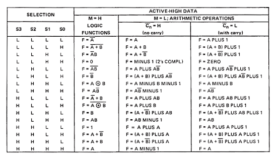
The 74181 implements a 4-bit ALU providing 16 logic functions and 16 arithmetic functions, as the datasheet (below) shows. As well as the expected addition, subtraction, and Boolean operations, there are some bizarre functions such as "(A + B) PLUS AB".

The datasheet for the 74181 ALU chip shows a strange variety of operations.

The datasheet for the 74181 ALU chip shows a strange variety of operations.

So how is the 74181 implemented and why does it include such strange operations? Is there any reason behind the 74181's operations, or did they just randomly throw things in? And why are the logic functions and arithmetic functions in any particular row apparently unrelated? I investigated the chip to find out.

The 16 Boolean logic functions

There's actually a system behind the 74181's set of functions: the logic functions are the 16 possible Boolean functions f(A,B). Why are there 16 possible functions? If you have a Boolean function f(A,B) on one-bit inputs, there are 4 rows in the truth table. Each row can output 0 or 1. So there are 2^4 = 16 possible functions. Extend these to 4 bits, and these are exactly the 16 logic functions of the 74181, from trivial 0 and 1 to expected logic like A AND B to contrived operations like NOT A AND B. These 16 functions are selected by the S0-S3 select inputs.

Arithmetic functions

The 74181's arithmetic operations are a combination of addition, subtraction, logic operations, and strange combinations such as "A PLUS AB PLUS 1". It turns out that there is a rational system behind the operation set: they are simply the 16 logic functions added to A along with the carry-in.2 That is, the arithmetic functions are: A PLUS f(A,B) PLUS carry-in. For example, If f(A,B)=B, you get simple addition: A PLUS B PLUS carry-in. If f(A,B) = NOT B, you get A PLUS NOT B PLUS carry-in, which in two's-complement logic turns into subtraction: A MINUS B MINUS 1 PLUS carry-in.

Other arithmetic functions take a bit more analysis. Suppose f(A,B) = NOT (A OR B). Then each bit of A PLUS f(A,B) will always be 1 except in the case where A is 0 and B is 1, so the result of the sum is A OR NOT B. Even though you're doing addition, the result is a logical function since no carry can be generated. The other strange arithmetic functions can be understood similarly.3

Thus, the 16 arithmetic functions of the 74181 are a consequence of combining addition with one of the 16 Boolean functions. Even though many of the functions are strange and probably useless, there's a reason for them. (The Boolean logic functions for arithmetic are in a different order than for logical operations, explaining why there's no obvious connection between the arithmetic and logical functions.)

Carry lookahead: how to do fast binary addition

The straightforward but slow way to build an adder is to use a simple one-bit full adders for each bit, with the carry out of one adder going into the next adder. The result is kind of like doing long addition by hand: in decimal if you add 9999 + 1, you have to carry the 1 from each column to the next, which is slow. This "ripple carry" makes addition a serial operation instead of a parallel operation, harming the processor's performance. To avoid this, the 74181 computes the carries first and then adds all four bits in parallel, avoiding the delay of ripple carry. This may seem impossible: how can you determine if there's a carry before you do the addition? The answer is carry lookahead.

Carry lookahead uses "Generate" and "Propagate" signals to determine if each bit position will always generate a carry or can potentially generate a carry. For instance, if you're adding 0+0+C (where C is the carry-in), there's no way to get a carry out from that addition, regardless of what C is. On the other hand, if you're adding 1+1+C, there will always be a carry out generated, regardless of C. This is called the Generate case. Finally, for 0+1+C (or 1+0+C), there will be a carry out if there is a carry in. This is called the Propagate case since if there is a carry-in, it is propagated to the carry out.4 Putting this all together, for each bit position you create a G (generate) signal if both bits are 1, and a P (propagate) signal unless both bits are 0.

The carry from each bit position can be computed from the P and G signals by determining which combinations can produce a carry. For instance, there will be a carry from bit 0 to bit 1 if P0 is set (i.e. a carry is generated or propagated) and there is either a carry-in or a generated carry. So C1 = P0 AND (Cin OR G0).

Higher-order carries have more cases and are progressively more complicated. For example, consider the carry in to bit 2. First, P1 must be set for a carry out from bit 1. In addition, a carry either was generated by bit 1 or propagated from bit 0. Finally, the first carry must have come from somewhere: either carry-in, generated from bit 0 or generated from bit 1. Putting this all together produces the function used by the 74181: C2 = P1 AND (G1 OR P0) AND (C0 OR G0 OR G1).

As you can see, the carry logic gets more complicated for higher-order bits, but the point is that each carry can be computed from G and P terms and the carry-in. Thus, the carries can be computed in parallel, before the addition takes place.5

Creating P and G with an arbitrary Boolean function

The previous section showed how the P (propagate) and G (generate) signals can be used when adding two values. The next step is to examine how P and G are created when adding an arbitrary Boolean function f(A, B), as in the 74181. The table below shows P and G when computing "A PLUS f(A,B)". For instance, when A=0 there can't be a Generate, and Propagate depends on the value of f. And when A=1, there must be a Propagate, while Generate depends on the value of f.

ABA PLUS f(a,b)PG
000+f(0,0)f(0,0)0
010+f(0,1)f(0,1)0
101+f(1,0)1f(1,0)
111+f(1,1)1f(1,1)

In the 74181, the four f values are supplied directly by the four Select (S pin) values, resulting in the following table:6

ABA PLUS fPG
00 0S10
01 1S00
10 11S2
11101S3

The chip uses the logic block below (repeated four times) to compute P and G for each bit. It is straightforward to verify that it implements the table above. For instance, G will be set if A is 1, B is 1 and S3 is 1, or if A is 1, B is 0 and S2 is set.

This circuit computes the G (generate) and P (propagate) signals for each bit of the 74181 ALU chip's sum. The S0-S3 selection lines select which function is added to A.

This circuit computes the G (generate) and P (propagate) signals for each bit of the 74181 ALU chip's sum. The S0-S3 selection lines select which function is added to A.

Creating the arithmetic outputs

The addition outputs are generated from the internal carries (C0 through C3), combined with the P and G signals. For each bit, A PLUS f is the same as P ⊕ G, so adding in the carry gives us the full 4-bit sum. Thus, F0 = C0 ⊕ P0 ⊕ G0, and similarly for the other F outputs.7 On the schematic, each output bit has two XOR gates for this computation.

Creating the logic outputs

For the logic operations, the carries are disabled by forcing them all to 1. To select a logic operation, the M input is set to 1. M is fed into all the carry computation's AND-NOR gates, forcing the carries to 1. The output bit sum as as above, producing A ⊕ f ⊕ 1 = A ⊕ f. This expression yields all 16 Boolean functions, but in a scrambled order relative to the arithmetic functions.8

Interactive 74181 viewer

To see how the circuits of the 74181 work together, try the interactive schematic below.9 The chip's inputs are along the top and right; click on any of them to change the value. The A and B signals are the two 4-bit arguments. The S bits on the right select the operation. C is the carry-in (which is inverted). M is the mode, 1 for logic operations and 0 for arithmetic operations. The dynamic chart under the schematic describes what operation is being performed.

The P and G signals are generated by the top part of the circuitry, as described above. Below this, the carry lookahead logic creates the carry (C) signals by combining the P and G signals with the carry-in (Cn). Finally, the sum for each bit is generated (Σ) from the P and G signals7, then combined with each carry to generate the F outputs in parallel.10

Result and truth table for inputs entered above
Select :

 0000
A0000
B0001
F1001
AiBiPiGiFi
00XYF
01XYF
10XYF
11XYF

Die photo of the 74181 chip.

I opened up a 74181, took die photos, and reverse engineered its TTL circuitry. My earlier article discusses the circuitry in detail, but I'll include a die photo here since it's a pretty chip. (Click image for full size.) Around the edges you can see the thin bond wires that connect the pads on the die to the external pins. The shiny golden regions are the metal layer, providing the chip's internal wiring. Underneath the metal, the purplish silicon is doped to form the transistors and resistors of the TTL circuits. The die layout closely matches the simulator schematic above, with inputs at the top and outputs at the bottom.

Die photo of the 74181 ALU chip. The metal layer of the die is visible; the silicon (forming transistors and resistors) is hidden behind it.

Die photo of the 74181 ALU chip. The metal layer of the die is visible; the silicon (forming transistors and resistors) is hidden behind it.

Conclusion

While the 74181 appears at first to be a bunch of gates randomly thrown together to yield bizarre functions, studying it shows that there is a system to its function set: it provides all 16 Boolean logic functions, as well as addition to these functions. The circuitry is designed around carry lookahead, generating G and P signals, so the result can be produced in parallel without waiting for carry propagation. Modern processors continue to use carry lookahead, but in more complex forms optimized for long words and efficient chip layout.12

I announce my latest blog posts on Twitter, so follow me at kenshirriff.

Notes and references

  1. Retro projects using the 74181 include the APOLLO181 CPU, Fourbit CPU, 4 Bit TTL CPU, Magic-1 (using the 74F381), TREX, Mark 1 FORTH and Big Mess o' Wires

  2. The carry-in input and the carry-out output let you chain together multiple 74181 chips to add longer words. The simple solution is to ripple the carry from one chip to the next, and many minicomputers used this approach. A faster technique is to use a chip, the 74182 look-ahead carry generator, that performs carry lookahead across multiple 74181 chips, allowing them to all work in parallel. 

  3. One thing to note is A PLUS A gives you left shift, but there's no way to do right shift on the 74181 without additional circuitry. 

  4. To simplify the logic, the 74181 considers 1+1+C both a Propagate case and a Generate case. (Some carry lookahead systems consider 1+1+C to be a Propagate case but not a Generate case.) For the 74181's outputs, Propagate must be set for Generate to be meaningful. 

  5. The carry-lookahead logic in the 74181 is almost identical to the earlier 74LS83 adder chip. The 74181's circuitry can be viewed as an extension of the 74LS83 to support 16 Boolean functions and to support logical functions by disabling the carry. 

  6. The way the S0 and S1 values appear in the truth table seems backwards to me, but that's how the chip works. 

  7. The bit sum Σ can be easily produced from the P and G signals. Some datasheets show each Σ signal generated as P XOR G, while other datasheets show Σ generated as NOT P AND G. Since the combination P=0, G=1 never arises, both generate the same results. I show XOR on the schematic as it is conceptually easier to understand, but examining the die shows the physical circuit uses the NOT/AND gates. 

  8. The logic functions are defined in terms of Select inputs as follows:

    ABF
    00S1
    00S0
    00S2
    00S3
    Because the first two terms are inverted, the logic function for a particular select input doesn't match the arithmetic function. 

  9. The schematic is based on a diagram by Poil on WikiMedia, CC By-SA 3.0, with circuitry and labeling changes. 

  10. The 74181 chip has a few additional outputs. The A=B output is used with the subtraction operation to test the two inputs for equality. The Cn+4 output is the inverted carry out, supporting longer words. P and G are the carry propagate and generate outputs, used for carry lookahead with longer words.11 

  11. The P and G outputs in my schematic are reversed compared to the datasheet, for slightly complicated reasons. I'm describing the 74181 with active-high logic, where a high signal indicates 1, as you'd expect. However, the 74181 can also be used with active-low logic, where a low signal indicates a 1. The 74181 works fine with active-low logic except the meanings of some pins change, and the operations are shuffled around. The P and G labels on the datasheet are for active-low logic, so with active-high, they are reversed. 

  12. One example of a modern carry lookahead adder is Kogge-Stone. See this presentation for more information on modern adders, or this thesis for extensive details. 

Analyzing the vintage 8008 processor from die photos: its unusual counters

The revolutionary Intel 8008 microprocessor is 45 years old today (March 13, 2017), so I figured it's time for a blog post on reverse-engineering its internal circuits. One of the interesting things about old computers is how they implemented things in unexpected ways, and the 8008 is no exception. Compared to modern architectures, one unusual feature of the 8008 is it had an on-chip stack for subroutine calls, rather than storing the stack in RAM. And instead of using normal binary counters for the stack, the 8008 saved a few gates by using shift-register counters that generated pseudo-random values. In this article, I reverse-engineer these circuits from die photos and explain how they work.

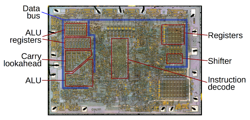
The image below shows the 8008's tiny silicon die, highly magnified. Around the outside of the die, you can see the 18 wires connecting the die to the chip's external pins. The 8008's circuitry is built from about 3500 tiny transistors (yellow) connected by a metal wiring layer (white). This article will focus on the stack circuits on the right side of the chip and how they interact with the data bus (blue).

The die of the Intel 8008 microprocessor, showing the stack and other important subcomponents.

The die of the Intel 8008 microprocessor, showing the stack and other important subcomponents.

For the 8008 processor's birthday, I'm using the date of its first public announcement, an article in Electronics on March 13, 1972 entitled "8-bit parallel processor offered on a single chip." This article described the 8008 as a complete central processing unit for use in "intelligent terminals" and stated that chips were available at $200 each.1

You might think that an intelligent terminal is a curiously specific application for the 8008 processor. There's an interesting story behind that, going back to the roots of the chip: the Datapoint 2200 "programmable terminal", introduced in June 1970. The popular Datapoint 2200 was essentially a desktop minicomputer with its processor consisting of a board full of simple TTL chips. The photo below shows the CPU board from the Datapoint 2200. The chips are gates, flip flops, decoders, and so forth, combined to build a processor, since microprocessors didn't exist at the time.

The processor board from the Datapoint 2200. The 8008 microprocessor was created to replace this board, but was never used by Datapoint. Photo courtesy of unknown source.

The processor board from the Datapoint 2200. The 8008 microprocessor was created to replace this board, but was never used by Datapoint. Photo courtesy of unknown source.

Processors typically use a stack to store addresses for subroutine calls, so they can "pop" the return address off the stack. This stack is usually stored in main memory. However, the Datapoint 2200 used slow shift-register memory2 instead of expensive RAM for its main storage, so implementing a stack in main memory would be slow and inconvenient. Instead, the Datapoint 2200's stack was stored in four i3101 RAM chips, providing a small stack of 16 entries. 3 4 The i3101 was Intel's very first product, and held just 64 bits. In the photo above, you can see the chips in their distinctive white packaging each with a large "i" for Intel. 5

To keep track of the top of the stack, the Datapoint 2200 used a 4-bit up/down counter chip to hold the stack pointer. The clever thing about this design is there's no separate program counter (PC) and stack; the PC is simply the value at the top of the stack. You don't need to explicitly push and pop the PC onto the stack; for a subroutine call you just update the counter and write the subroutine address to the stack.

The story of the 8008's origin is that Datapoint went to Intel and asked if Intel could build a chip that combined the stack memory and the stack pointer onto a single chip. Intel said not only could they do that, they could put the whole processor board onto a single chip! This was the start of Intel's 8008 project to duplicate the Datapoint 2200's processor board onto a chip, keeping the Datapoint 2200 instruction set and architecture.6 After various delays, Intel completed the 8008 microprocessor, but Datapoint rejected it. Intel decided to sell the 8008 as a general-purpose processor chip, sparking the microprocessor revolution. Intel improved the 8008 with the 8080 and then the 16-bit 8086, leading to the x86 architecture that dominates desktop and server computers today.

The consequence of the 8008's history is that it inherited its architecture and instruction set from the Datapoint 2200 intelligent terminal. One of these features was the fixed, internal stack. But the 8008's implementation of that stack is unusual.

Shift-register counter

The most unexpected part of the 8008's stack is how it keeps track of the current position. The straightforward way to implement the stack would be with a binary up/down counter to keep track of the current stack position (which is what the Datapoint 2200 did). But to save a few transistors, the 8008 uses a nonlinear feedback shift register instead of a counter. The result is the stack entries are accessed in a pseudo-random order! But since they are read and written in the same order, everything works out fine.

The shift register outputs are based on a de Bruijn sequence, a cyclic sequence in which every possible output occurs as a subsequence exactly once. The 8008's de Bruijn sequence is shown below. The first value (000) is underlined in red. Shifting to the blue position yields the second value (001). Proceeding around the circle clockwise yields all eight values in the sequence: 000, 001, 010, 101, 011, 111, 110, 100 and finally back to 000. Note that each value appears exactly once, but they are not in standard binary order.

8This de Bruijn sequence contains all eight 3-bit values as subsequences. 000 and 001 are underlined. The Intel 8008's internal counters are built form this sequence.

This de Bruijn sequence contains all eight 3-bit values as subsequences. 000 and 001 are underlined. The Intel 8008's internal counters are built form this sequence.

At each step in the sequence, the last two bits are shifted to the left and a new bit is placed on the right. Counting down is the converse: the first two bits are shifted to the right and a new bit is placed one the left. This process can be implemented with a shift register, a circuit that allows a bit sequence to be shifted and an additional bit inserted.7

The diagram below shows how the 8008 implements the nonlinear feedback shift register counter. While it make look complex, it's a straightforward implementation of the de Bruijn sequence. The three latches in the middle form a shift register, with each latch holding one bit. To count up, each bit is shifted to the left and a new bit is added on the right (green arrows). To count down, each bit is shifted to the right and a new bit is added on the left (purple arrows). The logic gate on the left generate the "new" bit for counting down and the gates on the right generate the new bit for counting up.

The 8008 uses the above circuit for its internal stack counter. The refresh counter is based on this, but counts up only.

The 8008 uses the above circuit for its internal stack counter. The refresh counter is based on this, but counts up only.

The logic gates may appear complex. However, one feature of PMOS logic is it's as simple to build an AND-OR-NOR gate as a plain NOR gate, just by wiring transistors in parallel or series. Designing the logic is also straightforward: for each triple of current bits, the de Bruijn sequence specifies the next bit. If you've studied digital logic, Karnaugh maps can be used to create the logic circuits to generate the desired next bit.

Inside the stack storage

The 8008 uses dynamic RAM (DRAM) to for its stack storage and its registers. The other 1970s microprocessors that I've examined use static latches, so the 8008 is a bit unusual in this regard. Since Intel was primarily a RAM company at the time, I assume they wanted to leverage their RAM skills and save transistors by using DRAM.

Each bit of storage in the 8008 uses a cell with three transistors and one capacitors, called a 3T1C cell, similar to the cell in Intel's i1103 DRAM chip. The diagram below shows a closeup of the 8008's stack storage, with six DRAM cells visible. Each row is one 14-bit address in the stack. Each row has a read enable and write enable control line coming from the left. Each column stores one of the 14 bits; the column sense line is used to read and write the selected bit.

Detail of the Intel 8008 microprocessor's die, showing six storage cells for the stack registers. Each bit is stored with a DRAM cell consisting of three transistors and a capacitor.

Detail of the Intel 8008 microprocessor's die, showing six storage cells for the stack registers. Each bit is stored with a DRAM cell consisting of three transistors and a capacitor.

The transistors for the first cell are labeled T1, T2 and T3. The value is stored on the capacitor labeled C. (There is no separate physical capacitor; the capacitance of the wiring is sufficient to store the bit.)

To write a bit, the write line for the desired row is pulled low, turning on T1. The desired voltage (low or high) is fed onto the sense line, passes through T1, and is stored by the capacitor. To read the value, the appropriate read line is pulled low, turning on T3. If C has a low voltage, T2 is turned on. This connects the sense line to ground through T3 and T2. On the other hand, if C has a high voltage, T2 is turned off and the sense line is not grounded. Thus, the circuitry connected to the sense line can tell what bit value is stored on C.

The inconvenience with dynamic RAM is that values can only be stored temporarily. After a few hundred microseconds, the charge stored on capacitor C will leak away and the value will be lost. The solution is a refresh circuit that periodically reads each value and writes it back, before the bit fades away. (A similar refresh process is used by your computer's RAM.) The 8008's internal RAM is refreshed at least every 240 microseconds, ensuring that bits are not lost. (Static RAM, on the other hand, uses a larger, more complex circuit for each bit, but will preserve the bit as long as the circuit is powered up.)

In the 8008, the stack storage (and the registers) are refreshed by continuously stepping through each entry: reading it and writing it back. To accomplish this, a second 3-bit shift-register counter is used as a refresh counter, tracking the current position that is being refreshed. The circuit for this is the same as the stack counter, except it omits the logic to count down, as it only needs to count in one direction.9

Understanding the die photo

I'll briefly explain what you're looking at in the die photo above. The chip itself is made from a silicon wafer. Plain silicon is essentially an insulator, but by doping it with impurities, it becomes a semiconductor. The dark lines indicate the boundary between doped and undoped regions; the doped silicon in the first cell is indicated in red.

On top of the silicon is the polysilicon layer, which is the yellowish stripes. Polysilicon acts as a conductor and is used as internal wiring of the chip. More importantly, a transistor is created when polysilicon crosses doped silicon. A thin oxide layer separates the polysilicon from the silicon, forming the transistor's gate. A low voltage on the polysilicon gate causes the transistor to conduct, connecting the two sides (called source and drain) of the transistor. A high voltage on the gate turns the transistor off, disconnecting the two sides. Thus, the transistor acts as a switch, controlled by the gate.

The top layer of the chip is the metal layer, which is also used as wiring. For the photo above, I removed the metal layer with hydrochloric acid to make the underlying silicon more visible. The green, blue and gray lines indicate where the metal wiring was before being removed. Transistors T1 and T3 are connected to the sense line (blue), while transistor T2 is connected to ground (green). The read and write lines enter the circuit on the left as metal wiring, connected to polysilicon lines.

The interface between the stack and the data bus

To access memory, the address in the stack must be provided to external memory via the 8 data/address pins on the chip. These pins are connected to the stack (and other parts of the 8008) via the data bus. The die photo below shows the circuitry that interfaces the 14-bit stack storage to the 8-bit data bus.11 At the top of the photo are the metal control lines and three of the data bus lines. At the bottom are the sense lines, discussed earlier, from the stack storage. In between are the transistors (orange) that connect the data bus and the stack.

The control lines select the low (L) or high (H) half of the address. These activate the appropriate read or write transistors, connecting the appropriate stack columns to the data bus.

The stack /bus driver circuit provides the "glue" between the data bus and the stack DRAM storage.

The stack /bus driver circuit provides the "glue" between the data bus and the stack DRAM storage.

The transistors to write an address to the data bus are much larger than typical transistors, appearing as vertical yellow bars in the die photo. The reason for this is the data bus passes through the whole chip. Due to the length of the bus, it has relatively high capacitance and larger, high-current transistors are required to drive a signal on the data bus.

Near the bottom of the photo are the inverter amplifiers. Each sense line is attached to an inverter that boosts the signal from the stack storage. During refresh, this boosted signal is written back, strengthening the bit stored on the capacitor.10

Conclusion

By examining die photos, it is possible to reverse-engineer the 8008 microprocessor. One unusual feature of the 8008 is that instead of using standard binary counters internally, it saves a few gates by using shift-register counters. Although these count in a pseudo-random order rather than sequentially, the 8008 still functions correctly. One counter is used for the on-chip address stack. The 8008 also uses DRAM internally for stack storage and register storage, requiring a second counter to refresh the DRAM. Since every transistor was precious at the dawn of the microprocessor age, the 8008 has these interesting design decisions that produced compact circuitry.

If you're interested in the 8008, my previous article has a detailed discussion of the architecture, more die photos and information on how to take them. This article explains the 8008's ALU.

I announce my latest blog posts on Twitter, so follow me at kenshirriff. I also have an RSS feed.

Notes and references

  1. The first announcement of the 8008 microprocessor in Electronics is shown below (click for a larger version). The announcement called the chip a "parallel processor", a term that had a different meaning back then, indicating that the processor operated on all 8 bits at the same time. This was in contrast to serial processors (such as the Datapoint 2200) that handled one bit of the word at a time.)

    The 8008 chip was announced in Electronics on March 13, 1972: "8-bit parallel processor offered on a single chip."

    The 8008 chip was announced in Electronics on March 13, 1972: "8-bit parallel processor offered on a single chip."

  2. In 1970, RAM memory chips were extremely expensive: $99.50 for an i3101 chip with just 64 bits of storage. Shift-register memory was cheaper and denser, with 512 bits of storage in an Intel 1405 chip. The big disadvantage is the bits were circulated around and around inside the chip, with only one bit available at a time. Sequential access wasn't a problem, but if you wanted to read memory out of order, you might need to wait half a millisecond for the right bit to circle around. I wrote about shift-register memories in detail here, with detailed die photos. 

  3. The i3101 memory was called the 3101 due to Intel's part numbering system at the time, described in Intel Technology Journal, Q1 2001. To summarize, the first digit indicate the product family: 1xxx is PMOS, 2xxx is NMOS, 3xxx is bipolar and so forth. The second digit indicates the product type: 1 is RAM, 2 is a controller, 3 is ROM, and so forth. The last two digits are sequence numbers typically starting with 01. Thus, the first bipolar RAM was the 3101.

    During development, the 8008 chip was called the 1201, following Intel's naming scheme: the 1 indicated the chip was built from PMOS technology, the 2 indicated a custom chip and the 01 was a serial number. Fortunately, when it came time to market microprocessors, Intel decided that marketing was more important than systematic numbering: Intel's 4-bit microprocessor became the 4004 and their 8-bit microprocessor the 8008. 

  4. Intel introduced the i3101 chip in April 1969. The i3101 RAM chip was a static memory chip, rather than the dynamic RAM chips common today. It was also built from Schottky TTL technology, rather than MOS used in modern RAM chips. Other companies, such as National Semiconductor, Signetics and Fairchild, made 64-bit memory chips compatible with the Intel i3101. However, they typically used the standard 74xx numbering scheme, calling the chip the 7489

  5. Although the Datapoint's stack could hold 16-bit values, the Datapoint 2200 only used 13 address bits, supporting a maximum of 8K of memory. The 8008 expanded the address range to 14 bits, supporting 16K of memory, which was a huge amount at that time. However, the 8008's internal stack was only 8 values, rather than the 16 of the Datapoint 2200. 

  6. Texas Instruments heard that Intel was designing a processor for Datapoint and asked Datapoint if they could build a processor for Datapoint too. TI beat Intel to the finish, creating the TMC 1795 processor before Intel completed the 8008, largely because Intel put the 8008 on the back burner. After Datapoint rejected TI's microprocessor, TI tried to find a new customer for the chip. TI was unsuccessful, and the TMC 1795 was abandoned and mostly forgotten. I've written about the TI chip in more detail here

  7. You may be familiar with linear-feedback shift registers (LFSRs), which can be used as pseudo-random number generators or noise generators. With N stages, a LFSR can generate 2N-1 output values. The de Bruijn sequence is generated from a nonlinear-feedback shift register. Nonlinear-feedback shift registers are a generalization of LFSRs; by using more complex feedback circuitry than just XOR, a nonlinear feedback shift register can generate sequences of arbitrary length. In particular, it can generate a sequence of 2N values, while a LFSR is limited to 2N-1. 

  8. Nonlinear feedback shift registers seem pretty obscure. The only other use I've seen is the TMS 0100 calculator chip, which generates an internal sequence of length 11. For information on the theory, see The Synthesis of Nonlinear Feedback Shift Registers and Counting with Nonlinear Binary Feedback Shift Registers. The book Shift Register Sequences goes into great detail on linear and nonlinear sequences; Section VII:5 is probably most relevant, describing how to make a shift register cycle of any length.

    The TMS 1000 microcontroller saves a few gates by using a LFSR for the program counter. Instead of incrementing, the PC goes through a pseudo-random sequence. The code is stored in the ROM in the same sequence; everything works out, but it seems like a strange way to implement a program counter. 

  9. I was expecting the stack counter and refresh counter to have a regular layout on the chip, with a single shift register stage repeated three times. However, on the 8008 die, the transistors are arranged irregularly, scattered around where there was room. Presumably this made the layout more compact. 

  10. Since the signal read from stack storage passes through an inverter before being written back, you might expect the bit to get flipped. The explanation is that transistor T2 in the storage cell inverts the value on C. Thus, the value read from a sense line is inverted compared to the value written on the sense line. The inverter amplifier provides a second inversion, restoring the original value. 

  11. Each 8008 instruction takes multiple clock cycles to execute. An instruction is broken into one or more machine cycles; each machine cycle typically corresponds to one memory access for instruction or data. Each machine cycle consists of up to 5 states (T1 through T5). An address is transmitted to memory during state T1 and T2, and the memory location is read or written during T3. Each T state requires two clock cycles, so an 8008 instruction takes a minimum of 10 clock cycles. The Intel 8008 user's manual provides detailed timings. 

Reverse-engineering the surprisingly advanced ALU of the 8008 microprocessor

A computer's arithmetic-logic unit (ALU) is the heart of the processor, performing arithmetic and logic operations on data. If you've studied digital logic, you've probably learned how to combine simple binary adder circuits to build an ALU. However, the 8008's ALU uses clever logic circuits that can perform multiple operations efficiently. And unlike most 1970's microprocessors, the 8008 uses a complex carry-lookahead circuit to increase its performance.

The 8008 was Intel's first 8-bit microprocessor, introduced 45 years ago.1 While primitive by today's standards, the 8008 is historically important because it essentially started the microprocessor revolution and is the ancestor of the x86 processor family that you are probably using right now.2 I recently took some die photos of the 8008, which I described earlier. In this article, I reverse-engineer the 8008's ALU circuits from these die photos and explain how the ALU functions.

Inside the 8008 chip

The image below shows the 8008's tiny silicon die, highly magnified. Around the outside of the die, you can see the 18 wires connecting the die to the chip's external pins. The rest of the chip contains the chip's circuitry, built from about 3500 tiny transistors (yellow) connected by a metal wiring layer (white).

Die photo of the 8008 microprocessor, showing important functional blocks.

Die photo of the 8008 microprocessor, showing important functional blocks.

Many parts of the chip work together to perform an arithmetic operation. First, two values are copied from the registers (on the right side of the chip) to the ALU's temporary registers (left side of the chip) via the 8-bit data bus. The ALU computes the result, which is stored back into the accumulator register via the data bus. (Note that the data bus splits and goes around both sides of the ALU to simplify routing.) The carry lookahead circuit generates the carry bits for the sum in parallel for higher performance.3 This is all controlled by the instruction decode logic in the center of the chip that examines each machine instruction and generates signals that control the ALU (and other parts of the chip).

The Arithmetic-Logic Unit

The 8008's ALU implements four functions: Sum, AND, XOR and OR. The Sum operation adds two 8-bit numbers. The remaining three operations are standard Boolean logic operations. The AND operation sets an output bit if the bit is set in the first AND the second number. OR checks if a bit is set in the first OR the second number (or both). XOR (exclusive-or) checks if a bit is set in the first OR the second number (but not both).

The concept of carries during addition is a key part of the ALU. Binary addition in a processor is similar to grade-school long addition, except with binary numbers instead of decimal. Starting at the right, each column of two numbers is added and there can be a carry to the next column. Thus, in each column, the ALU adds two bits as well as a carry bit.

In most early microprocessors, addition of each column needs to wait until the column to the right has been added and the carry is available. The carry "ripples" through the bits, right to left, slowing the addition. The 8008, however, uses a fast carry-lookahead circuit3 to generate the carries for all 8 columns in parallel before the addition happens. Then all the columns can all be added in parallel without waiting for the carry to "ripple" through the sum. This carry-lookahead circuit is an unusual feature to see in an early microprocessor due to its complexity.

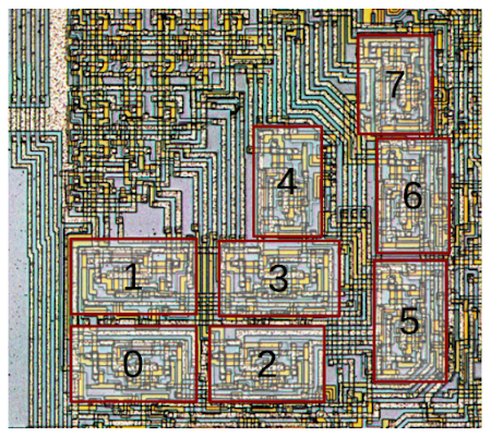
Since the 8008 is an 8-bit processor, the ALU operates on two eight-bit arguments. Most 8-bit processors (including the 8008) use a "bit-slice" construction for the ALU, with a one-bit ALU slice repeated eight times. Each one-bit ALU slice takes two input bits and the carry-in bit, and produces the output bit. In most 8-bit processors, the bit-slice ALU is arranged by stacking 8 rectangular ALU slices to form a compact, regular block. However, the 8008 has its eight ALU slices arranged in an irregular fashion—some blocks are even sideways—as shown in the diagram below. The motivation for this is that the carry lookahead circuit takes up a triangular space on the chip. To fit the remaining space better, the 8008's ALU is arranged into its unusual triangular layout.

Arrangement of the eight ALU slices on the 8008 microprocessor die. Unlike most processors, the 8008's ALU slices are arranged in a haphazard triangular arrangement. This fits better with the triangular carry-lookahead circuit above the ALU.

Arrangement of the eight ALU slices on the 8008 microprocessor die. Unlike most processors, the 8008's ALU slices are arranged in a haphazard triangular arrangement. This fits better with the triangular carry-lookahead circuit above the ALU.

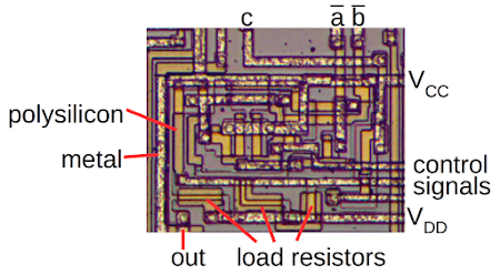
Zooming in on the die photo, we can look at one of the ALU slices and see how the circuitry is constructed. The chip is built from three layers (to simplify slightly). The topmost layer is the metal wiring. It is the most visible feature, and looks metallic (not surprisingly). In the detail below, you can see the horizontal and vertical metal traces. The polysilicon layer is underneath the metal layer and appears yellow/orange under the microscope. Polysilicon can act as wiring, but more importantly it forms the gates of the transistors, switching them on and off. The bottom layer is the grayish silicon die itself, but it is hard to see under the other layers.

Die photo of the 8008 processor, zoomed in on the circuit for one bit of the ALU.

Die photo of the 8008 processor, zoomed in on the circuit for one bit of the ALU.

In the diagram above, the carry c and the complemented a and b inputs enter through the metal wires at the top. The ALU output is at the bottom. The control signals are horizontal metal lines. The circuit is powered by the Vcc (+5 volts) and Vdd (-9 volts) metal lines. The brighter yellow polysilicon regions are transistors. Each gate in the circuit requires a "load resistor" connected to Vdd to pull its output low; for improved performance, these are implemented with transistors rather than resistors.

Removing the metal layer with acid makes the silicon and polysilicon layers more visible, as shown below.6 The chip is formed on a silicon wafer with regions of it "doped" with impurities to create regions of semiconducting silicon. You can see dark lines along the border between doped silicon and undoped silicon. A transistor is formed where a yellowish polysilicon wire crosses the doped silicon. The transistor forms a switch between the two silicon sides, controlled by the polysilicon gate. Each ALU slice contains 20 transistors; the diagram below points out two of them.5

With the metal layer removed from the 8008 processor die, the underlying silicon is visible. The photo shows bit 1 of the 8008's ALU.

With the metal layer removed from the 8008 processor die, the underlying silicon is visible. The photo shows bit 1 of the 8008's ALU.

Simulating one slice of the ALU

By examining the die photos carefully, you can map out the ALU slice's 20 transistors and their connections. From this, you can reverse-engineer the gates that make up the circuit. I explained in my previous article how PMOS gates are structured, so I won't go into the details here. The result is the schematic below, showing one bit of the ALU. Each ALU slice takes two inputs (a and b) and the input carry c, and outputs one result bit. There are three mode lines (m1, m2 and m3) that select one of the four ALU operations.7

The schematic below is interactive. First, select an operation and the table will update with results for the eight different inputs. Next, click a row in the table, and the schematic will update, showing how the ALU computes that row. (Note that the a and b inputs to the ALU are inverted, indicated by an overbar.)

Operation:

While this ALU slice looks like it is made of many gates, physically it is only three gates: two large, multilevel AND-OR-NAND gates and one NAND gate. The AND-OR-NAND logic is implemented on the chip as a single complex gate, rather than by combining simpler gates, since a single large gate provides better performance with less circuitry than multiple small gates. One feature of MOS logic is it's just as easy to form an AND-OR-NAND gate (for instance) as a plain NAND gate.

Understanding the ALU logic

The 8008's ALU circuit above looks like a mysterious collection of gates, but eventually I figured out the structure behind it. The starting point is a full adder that handles the Sum operation. (A full adder adds three input bits (a, b and c) and outputs the (low-order) sum bit and a carry bit.) The full adder is then heavily modified to support the logic operations, yielding the ALU from the previous section. The logic operations are implemented by using the mode lines to block parts of the circuit, yielding XOR, AND or OR, rather than the more complex Sum.

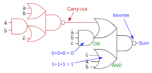
The diagram below strips down the 8008's ALU circuit to reveal the full adder "hidden" inside. The gate in red generates the carry-out from the three inverted inputs, using relatively straightforward logic. (Since the 8008 uses carry-lookahead, this carry-out signal isn't passed to the next ALU slice, but just used to generate the ALU output.) If you examine the possible sum cases, you will see that the sum bit is almost always just the carry-out inverted, except for the 0+0+0 and 1+1+1 cases. Thus, the sum bit can be generated by inverting the carry-out and handling the two exceptional cases.8 The two gates indicated below handle the exceptions by forcing the sum output to the correct value.

Simplified 8008 ALU slice, showing the full adder circuit.

Simplified 8008 ALU slice, showing the full adder circuit.

Comparing the full adder with the full ALU circuit earlier shows how the mode lines support the logic operations. Once you have a full adder, generating XOR is simply a matter of setting the carry-in to 0, which is done by the m3 control line. For the OR and AND operations, mode lines m3 and m2 respectively disable all of the circuit except the gates labeled in green.9 Thus, if you start with a full-adder and extend it to support XOR, AND and OR, the 8008's ALU circuit is a logical result.

Intel's earlier 4004 microprocessor had a simple ALU that only supported addition and subtraction, not any logic operations.10 Interestingly, the 4004's ALU circuit is almost identical to the full adder circuit shown above. So it's very likely that Intel designed the 8008 ALU by extending the 4004 ALU as described above. This would explain why the 8008's ALU generates carries internally, even though the carry lookahead circuit made this redundant.11

The 8008's ALU logic is very similar to the Z80's ALU,12 although the Z80's ALU is (surprisingly) 4 bits (details). The 8085 uses a different complex gate arrangement. The 6502 on the other hand, uses an entirely different approach: straightforward circuits for addition, AND, OR, XOR and shift-right, using pass-transistor multiplexers to select the operation.

Instruction decoding: how the ALU knows what operation to do

The 8008 executes 8-bit instructions, which move data, perform I/O, branch, call subroutines, and so forth. The instruction decoding logic examines the instruction and determines what operation to perform, generating about 30 control signals.13 Over a quarter of the instructions perform ALU operations, and the instruction set is carefully designed so three bits of the instruction specify which of the eight operations to perform.14 By examining these bits, the instruction decoder generates the ALU's mode control lines m1, m2 and m3.

Looking at AND instructions illustrates how this works. All AND instructions have the bit pattern xx100xxx (where x is either 0 or 1). For instance, the instruction to AND with memory is 10100111 and the instruction to AND with a constant is 00100100. When the instruction decode circuit matches this pattern, it pulls the m1 control line low, which causes the ALU to perform an AND operation.7 Other bit patterns generate the other ALU control signals.15

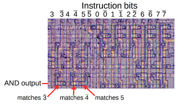
Part of the 8008's instruction decode PLA. The three indicated transistors match opcode pattern XX100XXX, indicating an AND instruction.

Part of the 8008's instruction decode PLA. The three indicated transistors match opcode pattern XX100XXX, indicating an AND instruction.

The diagram above shows part of the instruction decode circuit. The instruction bits (and their complements) are on yellow polysilicon wires running vertically through the circuit. Each row matches a bit pattern, with a transistor connected to each instruction bit to be matched. (The doped silicon regions forming transistors are the black outlines. Circles are connections between a transistor and the row's metal line.) For example, the three transistors marked with arrows match bit 3 low, bit 4 low, and bit 5 high, detecting the AND instruction pattern. Thus, the processor uses the grid of transistors in the instruction decoder to determine the meaning of each instruction.

Loose ends: Subtraction and rotating

The ALU implements a Sum operation, so you might wonder how subtraction is implemented. By using two's complement arithmetic, the CPU can perform subtraction by simply flipping all the bits on a value and then adding it. The ALU uses two temporary registers to hold the two operands since the ALU can't read the operands from the register file and write the result back simultaneously. One of the temporary registers has the feature that its value can be fed to the ALU directly or inverted. The subtraction instructions generate a signal causing the temporary register to provide the inverted value to the ALU, causing the ALU to perform subtraction.

One important operation in most processors is rotating or shifting the bits in a value, to the left or to the right. In most of the microprocessors I've examined, shifting is performed by the ALU.16 The 8008, on the other hand, implements the rotate logic in the register access circuit, on the opposite side of the chip from the ALU. When reading a register, the bits can be shifted one position left or right by a simple circuit before going onto the data bus.

History of the 8008

The Intel 8008 is important historically since it is the ancestor of the dominant Intel x86 architecture that you're probably using right now.2 I wrote a detailed article for the IEEE Spectrum on early microprocessor history, so I'll just give the outline of the 8008's complicated history here.

The 8008 copies the instruction set and architecture of the Datapoint 2200, a popular minicomputer introduced in 1970 as a programmable terminal.17 As was typical for minicomputers, the Datapoint 2200 contained a CPU build from individual TTL chips, filling up a circuit board. Datapoint contracted with both Intel and Texas Instruments to build a single-chip CPU that would replace this processor board, but keeping the same architecture and instruction set.

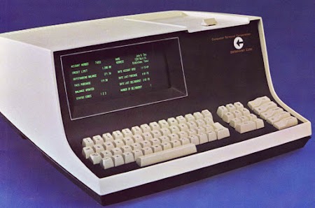
The Datapoint 2200 computer. The 8008 microprocessor was built to implement the Datapoint 2200's architecture and instruction set. Photo courtesy of Austin Roche.

The Datapoint 2200 computer. The 8008 microprocessor was built to implement the Datapoint 2200's architecture and instruction set. Photo courtesy of Austin Roche.

Texas Instruments was first to build a 2200-compatible microprocessor, creating the TMC 1795 chip. Intel got their version, the 8008, working a bit later, around the end of 1971. Datapoint rejected both processors, instead updating the Datapoint 2200 to use the 74181 TTL ALU chip. Texas Instruments couldn't find a new customer for the TMC 1795 and abandoned it. Intel, on the other hand, came up with the idea of selling the 8008 as a well-supported general-purpose processor. The 8008 led to the 8080, the 8085, 8086, and Intel's x86 line, which still retains some features of the 8008.

Conclusion

Although the 8008 was a very early microprocessor, its ALU was more advanced than you might expect. In particular, it used a complex carry-lookahead circuit for higher performance. Unfortunately, even with the carry-lookahead circuit, the 8008 was slower than the TTL-based Datapoint 2200 processor it was supposed to replace; addition took 20µs on the 8008, compared to 16µs on the original Datapoint 2200 and just 3.2µs on the upgraded Datapoint 2200. This illustrates the speed advantage that TTL had over MOS in the early 1970s. To us, a microprocessor may seem obviously better than a board of chips, but this wasn't always the case.

If you're interested in the 8008, my previous article has a detailed discussion of the architecture, more die photos and information on how to take them, and information on semiconductor history, so take a look.

I announce my latest blog posts on Twitter, so follow me at kenshirriff. I also have an RSS feed.

Notes and references

  1. The 8008 chip was publicly announced in an article in Electronics on March 13, 1972, entitled "8-bit parallel processor offered on a single chip", offering the chips for $200 each. 

  2. If you're not using an x86 processor right now, you're probably using an ARM processor. Don't feel neglected, though, since I've reverse-engineered the ARM-1 too. (Although there are many more ARM chips out there than x86, analytics show 71% of my readers are on x86.)  

  3. Using a carry look ahead circuit avoids the delay from a standard ripple-carry adder, where the carries propagate through the sum. The 8008's carry-lookahead is based on the Manchester carry chain, but with a separate carry chain for each carry, yielding the triangular structure you see on the die. For performance, the carry chain is implemented with dynamic logic, depending on wire capacitance, rather than with standard Boolean gates. The 74181 ALU chip in comparison, uses a different carry lookahead scheme implemented with standard logic. I plan to write more about the 8008's carry lookahead later. 

  4. The 8008 implements eight different arithmetic/logic functions: Add, Add with carry, Subtract, Subtract with borrow, AND, XOR, OR, and Compare.14 These are implemented in terms of the ALU's four basic operations. Subtraction is performed by inverting the second argument. The operations without carry/borrow clear the carry-in bit. Compare is simply a subtraction that doesn't store the result; it just sets the flags with the status. Thus, the four fundamental operations of the ALU are used to implement eight different arithmetic/logic operations. 

  5. Note that the 8008 uses PMOS transistors, rather than the faster NMOS transistors in later microprocessors such as the 8080, 6502 and Z80. If you're familiar with NMOS circuits, PMOS can be confusing since everything is backwards. PMOS transistors turn on if the gate is low, and typically pull the output high. Vdd in PMOS is negative, and "ground" is positive. The "pull-up resistor" in a PMOS gate pulls the output down. A PMOS NAND gate has transistors in parallel (compared to serial for an NMOS NAND gate). A PMOS NOR gate has transistors in serial (compared to parallel for an NMOS NOR gate). 

  6. The metal layer of the chip is protected by silicon dioxide passivation layer. The professional way to remove this layer is with dangerous hydrofluoric acid. Instead, I used Armour Etch glass etching cream, which is slightly safer and can be obtained at craft stores. I applied the etching cream to the die and wiped it for four minutes with a Q-tip. (Since the cream is designed for frosting glass, it only etches in spots. It must be moved around to obtain a uniform etch.) After this, I soaked the die in hydrochloric acid (pool acid from the hardware store) overnight to dissolve the metal. This was probably too long, since the edges of the polysilicon were eaten away in places. 

  7. The following values are used for the three mode lines to select the ALU function:

    Operationm1m2m3
    Sum111
    And010
    Or100
    Xor110
     

  8. A more straightforward way of generating the sum bit is by xoring the three inputs: a⊕b⊕c. Unfortunately, an XOR gate is relatively difficult to implement with Boolean logic, so designers will often try to avoid XOR. 

  9. You might wonder why the OR operation is implemented with an AND gate, and vice versa. Since the inputs and the output of the OR gate are inverted, this is equivalent to an AND gate (by De Morgan's laws), and similarly for the AND gate. 

  10. Strictly speaking, the 4004 microprocessor has an AU (arithmetic unit), not an ALU (arithmetic/logic unit), since it doesn't do logical operations. Since the 4004 was designed for a calculator, logical operations weren't required. 

  11. The 8008's full adder generates the carry-out first, and generates the sum from that. In contrast, the typical full adder circuit combines two half adders to generate the sum and carry-out separately. If the typical full adder circuit had been used in the 8008, the carry-out logic could easily be omitted. 

  12. To see the similarity between the Z80's ALU circuit and the 8008's, you need to swap AND and OR gates. (Apply De Morgan's laws since the 8008's ALU inputs are inverted.) In the Z80, the carry-out comes from the ALU rather than a carry-lookahead circuit, so the control lines are somewhat different. But the fundamental ALU circuit is otherwise the same between the 8008 and Z80, which is not surprising since Federico Faggin worked on both chips. 

  13. Instruction decoding is based on a Programmable Logic Array (PLA), an arrangement of transistors that efficiently implements logic gates. These gates match bit patterns and generate the appropriate control signals for the rest of the chip. The 8008's PLA has 16 input lines flow vertically through the PLA. Each row in the PLA matches a bit pattern and generates a control signal output.

    In more detail, each row output line is pulled low by a load resistor/transistor to Vdd. The transistors are connected between the row line and Vcc (+5V). The bit lines are connected to the transistor's gate. If any bit line is low (indicating a mismatch), the PMOS transistor turns on, pulling the row line high. Thus, if there is no mismatch, the control line is low, and if there is a mismatch, the control line is high. In other words, each row is a NAND gate with instruction bit inputs.

    The input lines are ordered as follows: bit 3, bit 3 complement, 4, 4', 5, 5', 0, 0', 1, 1', 2, 2', 6, 6', 7, 7'. This order may seem strange, but there's a reason for it. In the 8008, the ALU operation is selected by bits 3, 4 and 5 of the instruction. By putting those bits on the left side of the PLA, they are closer to the ALU. Some rows of the PLA actually decode two instructions: bits 3, 4 and 5 are decoded on the left side, generating an ALU control signal, while the remaining bits are decoded on the right side generating a different control signal. This increases the PLA density and saves space on the chip. 

  14. The 8008's instruction set is designed around octal. Among other things, there are 8 ALU operations, 8 registers and 8 conditionals. In octal, the ALU instructions have the value 2ar, where a is the ALU operation to perform (0 through 7) and r is the register to use (0 through 7, where 7 indicates memory). The octal structure originates with the Datapoint 2200, which decoded instructions with TTL 7442 BCD chips that decoded groups of three bits. This octal structure persisted in descendants of the 8008, including the Z80 and x86. Unfortunately, these instruction sets are almost always presented in hexadecimal, which hides the underlying structure. 

  15. The instruction decoder generates all the signals required by the ALU. As described above, AND matches xx100xxx, pulling the m1 control signal low. An OR opcode has the bit pattern xx110xxx, which causes the instruction decode circuit to pull the m2 control line low. An XOR instruction has the bit pattern xx101xxx. The m3 control line is pulled low for patterns xx10xxxx or xx1x0xxx, matching AND, OR or XOR instructions. The subtract (with and without borrow) instructions match xx01xxxx, generating a signal that inverts the second argument. 

  16. Different processors use a variety of techniques for shifting. In the Z80, shifting is performed as data enters the ALU. The 6502 performs a left shift with "A plus A", and has a path inside the ALU for right shifts; the 8085 is similar. The ARM-1 has a barrel shifter next to the ALU that performs arbitrary shifts. 

  17. The instruction set of the Datapoint 2200 is described in the Reference Manual. The 8008 has a couple minor changes. For instance, the 8008 has increment and decrement instructions that are not present in the 2200. 

Inside the 74181 ALU chip: die photos and reverse engineering

What's inside a TTL chip? To find out, I opened up a 74181 ALU chip, took high-resolution die photos, and reverse-engineered the chip.1 Inside I found several types of gates, implemented with interesting circuitry and unusual transistors. The 74181 was a popular chip in the 1970s used to perform calculations in the arithmetic-logic unit (ALU) of minicomputers. It is a moderately complex chip containing about 67 gates and 170 transistors3, implemented using fast and popular TTL (transistor-transistor logic) circuitry.

The 74181 die photo is below. (Click the image for a high-resolution version.) The golden stripes are the metal layer that interconnects the circuitry of the chip. (It's not gold, just aluminum that looks golden from the lighting.) The white squares around the edge of the die are the pads that are connected by tiny bond wires to the external pins. Under the metal layer is the silicon that makes up the chip. Faint lines show the doped silicon regions that make up the transistors and resistors. While the chip may appear impossibly complex at first, with careful examination it is possible to understand how it works.

Die photo of the 74181 ALU chip.

Die photo of the 74181 ALU chip.

The 74181 chip is important because of its key role in minicomputer history. Before the microprocessor era, minicomputers built their processors from boards of individual chips. The arithmetic operations (addition, subtraction) and logical operations (AND, OR, XOR) were performed by the arithmetic/logic unit (ALU) in the processor. Early minicomputers built ALUs out of a large number of simple gates. But in March 1970, Texas Instruments introduced the 74181 Arithmetic / Logic Unit (ALU) chip, which put a full 4-bit ALU on one fast TTL chip.4 This chip provided 32 arithmetic5 and logic functions2, as well as fast carry lookahead.7 Using the 74181 chip simplified the design of a minicomputer processor and made it more compact, so it was used in many minicomputers. Computers using the 74181 ranged from the popular PDP-11 and NOVA minicomputers to the powerful VAX-11/780 to the Datapoint 2200 desktop computer. The 74181 is still used today in retro hacker projects.6

A brief guide to NPN transistors

The 74181 is built from bipolar NPN transistors, a different technology from the MOS transistors in modern processors. The diagram below shows how an NPN transistor appears in an integrated circuit, along with a cross section. The transistor has three connections: the collector, base and emitter, with metal lines for each. The collector is connected to N-type silicon, the base to P silicon, and the emitter to N silicon (giving it the NPN structure). On the chip, you can recognize the emitter from its nested squares, the base because its silicon region surrounds the emitter, and the collector because it is the largest contact.

Structure of an NPN transistor appears in an IC.

Structure of an NPN transistor appears in an IC.

The key idea of the NPN transistor is it acts as a switch between the collector and emitter, controlled by the base. Normally there is no current flow between the collector and the emitter, so it's like a switch in the "off" position. But if you pass a small current from base to emitter, the transistor allows a large current from collector to emitter, like a switch in the "on" position. (This is vastly oversimplified—bipolar transistors are much more "analog"—but should be enough to understand how the 74181 works.) At the right is the symbol for an NPN transistor with the collector, base and emitter labeled.

Inverter

The fundamental component of TTL logic is the inverter, and other gates are modifications of the inverter circuit. Thus, it's important to understand the basic construction of the inverter, even though it is a bit complicated. I'll explain how it works in an oversimplified way.9

The diagram below shows an inverter in the 74181 chip. The 5V and ground lines run vertically along the left, powering the inverter. The transistors are highlighted with boxes. The resistors are visible as long strips of doped silicon snaking around.11 An input pin (A0) is wired to the pad. On the right is the schematic for a TTL inverter10, with components highlighted to match the die photo.

An inverter in the 74181 ALU chip, along with a schematic showing the components of the inverter.

An inverter in the 74181 ALU chip, along with a schematic showing the components of the inverter.

The input is connected to transistor Q1 (red). This transistor is used in an unusual way, acting as a "current-steering" transistor. If the input is low, R1's current is steered through Q1's emitter to the input, leaving Q2 off. If the input is high, R1's current flows "backwards" out Q1's collector to Q2's base, turning on Q2. Transistor Q2 (orange) can be considered a "phase splitter transistor", which makes sure that exactly one of the output transistors (Q3 and Q4) is activated. (That is, they turn on in opposite phases.) If Q2 is off, R2 provides current to turn on Q3 (yellow), which pulls the output high. Meanwhile, R3 turns off Q4. On the other hand, if Q2 turns on, it provides enough current to turn on Q4 (green), which pulls the output low. I'll explain the diodes in a footnote.12

The 74181 schematic

The schematic below13 shows the circuitry of the 74181. If you've taken a digital logic course, you've probably seen how to build a full adder circuit. But if you look at the schematic of the 74181, it's implemented in a very different way, to provide higher speed and more flexibility.8 The main reason for its complexity is it computes everything in parallel, rather than waiting for the carry to ripple from bit to bit, and this requires a lot more logic.

The different types of gates are highlighted. There are a few inverters (red) to invert input signals. Most of the logic consists of AND-OR-INVERT gates. The AND stages are shown in blue, and the OR-INVERT (NOR) stages in green. (Some of the OR-INVERT stages are not explicit on the schematic and are empty boxes.) The chip uses a few XOR gates (purple) to compute sums. Finally, there are a couple unique gates shown in yellow.

Schematic of the 74181 ALU.

Schematic of the 74181 ALU.

The schematic can be matched up with the labeled die image below. Conveniently, the layout of the die largely matches the schematic. The AND-OR-INVERT gates make up the majority of the chip. Also notice the large chip real estate used for resistors. The chip pins are labeled with blue text. (The metal layer was removed for this photo, to make the underlying circuitry more visible.)

The 74181 ALU die, with main gate types outlined.

The 74181 ALU die, with main gate types outlined.

AND-OR-INVERT

Most of the 74181's logic is implemented with AND-OR-INVERT gates, which consist of AND gates connected to a NOR gate as shown below. After seeing the inverter, you may expect that an AND-OR-INVERT gate is very complex. But as the schematic below14 shows, the AND-OR-INVERT is not much more complex than an inverter, requiring just a few more transistors. An AND gate is implemented by adding more emitters to the current-steering input transistor (red). (This may seem very strange, but transistors with multiple emitters are common in TTL circuits.) If all inputs are high, the base current will be steered to the collector. Otherwise, the base current will flow out the emitter. Thus, the AND of the inputs is generated. The NOR gate is implemented by putting phase splitter transistors in parallel (orange). If any of the bases are high, the corresponding transistor (Q2A or Q2B) will conduct, pulling the output low. While the circuit below has two AND gates, it can easily be extended to as many gates and inputs as desired.

The AND-OR-INVERT circuit from the 7451 chip. The multiple-emitter transistors that implement AND are highlighted in red. The transistors that implement OR are highlighted in orange.

The AND-OR-INVERT circuit from the 7451 chip. The multiple-emitter transistors that implement AND are highlighted in red. The transistors that implement OR are highlighted in orange.

The diagram below shows how these multiple-emitter transistors are implemented on the chip. Three of these transistors are shown, each with four or five emitters (the dark squares), creating 4-input or 5-input AND gates. Each transistor's base is at the top and each collector is at the bottom. The signal lines run horizontally, with emitters connected as needed. With this structure, multiple AND gates can arranged efficiently on the chip (similar to a Programmable Logic Array or PLA). Note that the base resistors take up a significant amount of space.

Three AND gates in the 74181 ALU chip. Each one is a single transistor with multiple emitters.

Three AND gates in the 74181 ALU chip. Each one is a single transistor with multiple emitters.

The diagram below shows how the OR-INVERT part of the circuit appears on the chip. Note that Q2A and Q2B (orange) share a collector, so the two transistors don't take up much space on the die. Their inputs come from AND circuits such as the ones above. 3-input and 4-input OR gates are implemented similarly, by adding more transistors.

The OR-INVERT stage of the AND-OR-INVERT gate in the 74181, compared with the 7451 AND-OR-INVERT gate.

The OR-INVERT stage of the AND-OR-INVERT gate in the 74181, compared with the 7451 AND-OR-INVERT gate.

Exclusive-OR

The chip uses a clever, compact circuit to compute XOR with two transistors wired in an unusual way: the emitters and bases are tied together and there is no connection to ground. The way it works is if the first input is high and the second is low, the first transistor turns on due to the base-emitter current. This pulls the output low through the transistor, with the second input acting as ground. Likewise, if the first input is low and the second is high, the second transistor turns on and pulls the output low. If both inputs are the same, there is no base-emitter current, both transistors remain off, and the output is pulled high by the resistor. The output from the transistor pair goes to the standard inverter stage, so the resulting signal is the XOR of the two inputs. 15 As with OR-INVERT, the two transistors share a collector, making the layout more compact.

The circuit used in the 74181 to compute XOR. Layout inspired by userbinator.

The circuit used in the 74181 to compute XOR. Layout inspired by userbinator.

A few things to note about the photo. The two transistors share a collector, which is equivalent to wiring their collectors together. The pull-up resistor doesn't appear in the photo; it is off to the right. The inputs to the XOR are from AND-OR-INVERT gates; their output transistors are at the top of the photo.

NOT-AND

The chip uses four AND gates that have one inverted input.17 On the die, it appears at first that the gates are implemented with the standard AND transistors, but an interesting trick is used to invert one of the inputs. Transistor Q1 is wired in the normal current-steering way, with R1 providing a base current. But transistor Q2 has its resistor connected to the collector, not the base.16 Normally R2 will pull the output high. But if input X is high and input Y is low, R1's current will go through Q1's collector and Q2's emitter, turning on Q2 and pulling the output low. Thus, the result after the inverter stage will be X AND NOT Y.

The 74181 uses an interesting circuit to generate NOT-AND. It uses the multi-emitter transistors but in a subtly different way from the AND gates.

The 74181 uses an interesting circuit to generate NOT-AND. It uses the multi-emitter transistors but in a subtly different way from the AND gates.

Getting the die photos

To create die photos, the integrated circuit package must be opened to expose the silicon die inside. Most chips have an epoxy package, which can be dissolved in boiling sulfuric acid. Since I don't like boiling acid, I obtained the 74181 chip in a ceramic package, which is much easier to open.

The 74181 ALU chip in a ceramic package.

The 74181 ALU chip in a ceramic package.

I tapped the chip along the seam with a chisel, splitting the two layers apart. Below, you can see how the metal pins are mounted between the layers, and are connected to the silicon die with tiny bond wires.

By tapping the 74181 chip with a chisel, the ceramic package can be popped open.

By tapping the 74181 chip with a chisel, the ceramic package can be popped open.

To photograph the die, I used a metallurgical microscope, a special type of microscope that shines light down through the lens to illuminate the chip from above. I took 22 photographs and then used the Hugin stitching software to combine them into a high-resolution image (details). Then, I removed the metal layer from the chip with hydrochloric acid and took more images, resulting in the image below. Removing the metal makes it easier to see the structure of the silicon layer and determine how the chip works. (Click for high-resolution version.)

Removing the metal layer of the 74181 chip with HCl reveals the silicon layer underneath.

Removing the metal layer of the 74181 chip with HCl reveals the silicon layer underneath.

Conclusion

The 74181 ALU chip is a complex, high-performance TTL chip that was a key component in the processor of many minicomputers. I took detailed die photos of the 74181 ALU that reveal how the chip works internally. It uses several different logic gates, primarily AND-OR-INVERT gates that have an efficient layout on the chip. These gates are implemented by extending an inverter circuit in different ways, but are more complex than their MOS equivalents. I plan to explain how the 74181 implements its 32 functions and fast carry in a future article, so keep watching.

I announce my latest blog posts on Twitter, so follow me at kenshirriff. I also have an RSS feed.

Notes and references

  1. To understand what's inside a TTL chip, it might be more sensible to start with a simple chip such as a NAND gate. But why take the easy way when there's a complex chip to explore? 

  2. Many of the 74181's 32 functions are strange, but there is actually a system behind it. Note that there are exactly 16 possible functions on two (one-bit) binary inputs A and B. (There are 4 lines in the truth table, and two choices for each output, so 2^4 possible functions.) The 74181's 16 logic functions are simply these 16 functions (extended to 4 bits). The 74181's 16 arithmetic functions are A PLUS (one of the 16 possible functions of A and B) PLUS carry-in. 

  3. Various sources say the 74181 has 61 or 75 gates. The schematic shows 67 gates. If you omit the five 1-input AND gates, you get 62 gates, i. On the die, I counted 169 transistors, but it's quite possible I missed some. 

  4. The history of the 74181 chip is described in detail on this site. The 74181 is apparently the first ALU chip created. In 1968, Fairchild introduced the 3800, an 8-bit accumulator chip, but it didn't have logical functions so technically it's just an AU (Arithmetic Unit) not an ALU like the 74181. Before the 74181 was the 7483 4-bit adder chip (1968); internally, the 7483 is similar to the lower half of the 74181. The 7483 was used in minicomputers such as the PDP 8/E. 

  5. ALU chips of this era didn't perform multiplication or division, let alone floating point operations. Multiplication and division operations were common in computers of that era, but were typically performed with multiple cycles of addition or subtraction. The one operation that seems missing from the 74181 is "shift right"; it can do a shift left with "A PLUS A". 

  6. Retro projects using the 74181 include the APOLLO181 CPU, Fourbit CPU, 4 Bit TTL CPU, Magic-1 (using the 74F381), TREX, Mark 1 FORTH and Big Mess o' Wires

  7. When multiple 74181 chips are connected together for larger words, you can simply feed the carry-out of one chip into the carry-in of the next. For higher performance, the 74182 look-ahead carry generator could be used to compute the carries across multiple chips in parallel. Some minicomputers (such as the Xerox Alto) didn't use the 74182, while others (such as the Interdata 7/16) did. 

  8. I'll give a brief overview of the chip's implementation here. The chip is build around the idea of carry lookahead. In particular, the upper and-or-invert gates create the carry P (propagate) and G (generate) signals for each bit of A PLUS f(A,B). The lower and-or-invert gates use these signals to compute the carry for each bit of the sum. Finally, the xor gates add the P, G and carry to compute each final sum. The point of this implementation is to compute the four bits in parallel and avoid a slow ripple carry. In a later post I'll explain this circuitry in full detail. 

  9. I've simplified the discussion of the TTL logic circuit, since most people probably don't care about saturation, β, biasing, and so forth. If you want the full analysis, see Logic gates: the NOT gate or Transistor-Transistor Logic. This presentation shows schematics for the different gates and TTL logic families. 

  10. The inverter schematic is from the datasheet of the common 7404 inverter chip. Interestingly, the basic circuit used in an inverter chip is almost identical to the circuit used inside the 74181. This turns out to be true for most of the 74181 circuits—they are similar to individual TTL parts. The 74181's transistors are a bit smaller because not as much current is required inside the chip, but there is much less scaling than you might expect. 

  11. In the 74181's inverter, R4 is not used. R1 takes its place. This is probably because an inverter in the chip doesn't need to provide as much current as a 7404 inverter chip. 

  12. The tricky part of the inverter circuit is that if Q2 turns on, there's enough voltage to turn on Q4 but not Q3, thanks to diode D2. The purpose of diode D2 isn't to conduct current in one direction, like you'd expect from a diode. Instead, its purpose is to raise Q3's emitter voltage by one diode drop (about 0.7V). As a consequence, Q3 requires 0.7V more at the base to turn on. Thus, when Q2 is active, there is enough voltage to turn Q4 on, but not Q3. And diode D1 simply protects the chip by shunting any negative input voltage to ground. 

  13. The schematic is based on a diagram by Poil on WikiMedia, CC By-SA 3.0, with labeling changes and gates highlighted. 

  14. The AND-OR-INVERT schematic is slightly modified from the 7451 AND-OR-INVERT chip to match the 74181's circuit. The 74181's AND-OR-INVERT circuits in the lower half of the chip omit the pull-up output transistor found in the 7451 since the 74181 doesn't require as much output current internally. (The output diode remains to drop the phase splitter transistor's collector voltage by one diode drop, or else the low output voltage will be too high.) 

  15. The circuit used in the 74181 for exclusive-OR is similar to the 7486 TTL XOR chip

  16. On the die, Q2 appears to have two collectors. But these are just two contacts to the same collector, to simplify routing of the wiring. This is unlike the multiple-emitter transistors, which genuinely have multiple emitters. 

  17. Some datasheets (example) show an XOR gate instead of NOT-AND. You might wonder how this could possibly work since XOR and NOT-AND are different. The answer is that one of the four input combinations never happens in the 74181, and the gates are equivalent across the other three inputs. The physical implementation is NOT-AND rather than XOR.