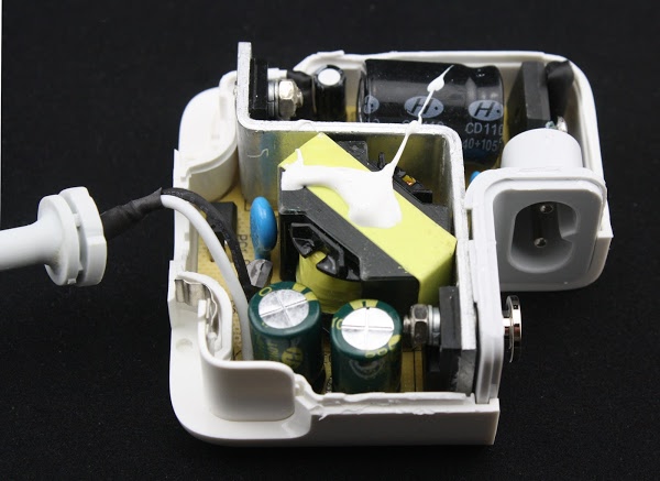
Inside card sorters: 1920s data processing with punched cards and relays

Punched card sorters were a key part of data processing from 1890 until the 1970s, used for accounting, inventory, payroll and many other tasks. This article looks inside sorters, showing the fascinating electromechanical and vacuum tube circuits used for data processing in the pre-computer era and beyond.

Herman Hollerith invented punch-card data processing for the 1890 US census.[1] Businesses soon took advantage of punched cards for data processing, using what was called unit record equipment. Each punched card held one data record, consisting of multiple data fields. A card sorter sorted the cards into the desired order. Then a machine called a tabulator read the cards, added up desired fields and printed a report.

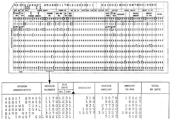
For example, a company could have one card for each invoice it needs to pay, as shown below, with fields for the vendor number, date, amount to pay, and so forth. The card sorter ordered the cards by vendor number. Then the tabulator generated a report by reading each card and printing a line for each card. Mechanical counters in the tabulator summed up the amounts, computing the total amount payable. Many other business tasks such as payroll, inventory and billing used punched cards in a similar manner.

Example of a punched card holding a 'unit record', and a report generated from these cards. From Functional Wiring Principles.

Example of a punched card holding a 'unit record', and a report generated from these cards. From Functional Wiring Principles.

The surprising thing about unit record equipment is that it originally was entirely electro-mechanical, not even using vacuum tubes. This equipment was built from components such as wire brushes to read the holes in punched cards, electro-mechanical relays to control the circuits, and mechanical wheels to add values. Even though these systems were technologically primitive, they revolutionized business data processing and paved the way for electronic business computers such as the IBM 1401.

How a sorter works

A card sorter takes punched cards and sorts them into order based on a field, for example employee number, date, or department. One application is putting records in the desired order when printing out a report.[2] Another application is grouping record by a field, for instance to generate a report of sales by department: the cards are first sorted based on the department field, and then a tabulator sums up the sales field, printing the subtotal for each department.

To sort punched cards, they are loaded into the card hopper and fed through the sorter. Cards are read and directed into one of the 13 card pockets: 0 through 9, two "zone" pockets, and a Reject pocket. This is very different from a typical sort algorithm — cards aren't compared with each other — so you may wonder how this machine sorts its input.

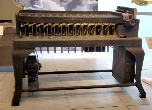
IBM Type 80 Card Sorter.

IBM Type 80 Card Sorter.

Card sorting uses a clever technique called radix sort. The sorter operates on one digit of the field at a time, so to sort on a 3-digit field, cards are run through the sorter three times. First, the sorter deposits the cards into ten bins (0-9) based on the lowest digit of the field. The operator gathers up the cards from the bins in order (0 bin first and 9 bin last) and they are sorted again on the second-lowest digit, again getting stacked in bins 0-9. The important thing is that the cards in each bin will still be ordered from the first pass: bin 0 will have cards ending in 00 first, and cards ending in 09 last. The operator gathers up the cards in order again, yielding a stack that is now sorted according to the last two digits. The cards are run through the sorter a third time, this time sorting on the third-lowest digit. After the last run through the sorter, the cards are in order, sorted on the entire field.

The radix sort process is fast and simple. You may be familiar with comparison-based sorting algorithms like quicksort that compare and shuffle entries, taking O(n log n) time. Radix sort can be implemented with a simple electric mechanism (along with an operator busily moving stacks of cards around), and takes linear time.[3] Although the sorter's hopper can hold 3600 cards, it can sort as many cards as desired, as long as the operator keeps loading and unloading them.

The sorting mechanism

You might expect a sorter to have multiple sensors to read the holes from a card and 10 flippers to direct the card into the right bin. But the actual implementation of the early sorters is amazingly simple and clever, using a single sensor and a single electromagnet.

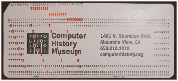
An IBM punched card, showing the encoding of digits and letters.

An IBM punched card, showing the encoding of digits and letters.

The photo above shows the layout of a standard IBM punched card, which stores 80 characters in 80 columns. The characters are printed along the top of the card and the corresponding holes are punched below. For a digit, each column has a single punch in row 0 through 9 to indicate the digit in that column. (I'll explain the two additional "zone" rows for alphabetic characters later.)

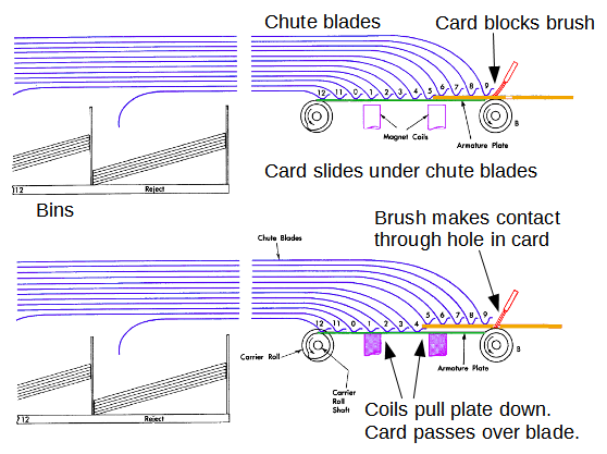
The diagram below shows how the card sorter works. Cards are fed through the sorter "sideways" starting with the bottom edge (called the "9-edge" because the bottom row is row 9). A small wire brush (red) detects the presence or absence of a hole; the brush will contact the rows in order from 9 to 0. An intact card blocks the wire brush from contacting the metal roller. But if there is a hole in the card, the brush makes contact with the roller through the hole, completing an electrical circuit.

Card sorting mechanism in the IBM Type 80 card sorter.

Card sorting mechanism in the IBM Type 80 and Type 82 card sorter.

A stack of metal guides (called chute blades) is used to direct the card into the appropriate bin. As a card is fed through the sorter mechanism, it slides under the chute blades as shown in the top illustration. If the brush (red) makes contact through a hole, it trips an electromagnet (purple) that pulls down a metal armature plate (green), allowing the ends of the chute blades to drop down. This causes the card to go above the chute blade rather than underneath it. The key is the chute blades have the same spacing as the rows on the card so the hole is detected just before the card reaches the corresponding blade. (If no hole is detected, the card passes under all the chute blades and into the Reject bin.)

For example, in the diagram above the card has slid under chute blades 9 through 5. The brush makes contact through hole 4, energizing the electromagnet and causing the blades to drop just before the card reaches blade 4. Thus, the card is directed into chute 4.

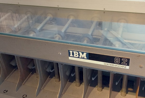
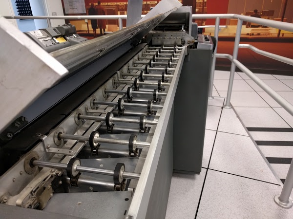
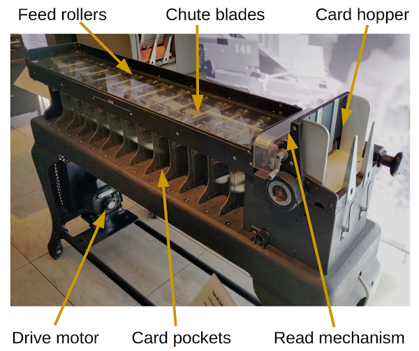
The chute blades can be seen in the photo below; they are the metal strips running down the center of the sorter between the feed rollers. Each chute blade ends at the appropriate pocket, causing the card to drop into the right location.

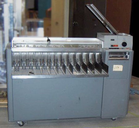
IBM Type 82 Card Sorter. The feed rollers under the glass top send cards through the sorter. The pockets at bottom collect the cards. This is a German model, thus the 'Sorteirmaschine' label.

IBM Type 82 Card Sorter. The feed rollers under the glass top send cards through the sorter. The pockets at bottom collect the cards. This is a German model, thus the 'Sorteirmaschine' label.

Alphabetic sorting

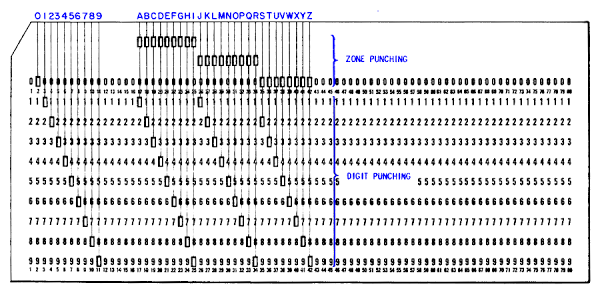
Numeric values have one hole in a column and are straightforward to sort, but how about alphabetic characters? In addition to the ten numeric rows 0-9, punched cards also have two additional "zone" rows (11 and 12). The diagram below shows the encoding; a letter combines a digit punch (1-9) with a zone punch (a hole in 0, 11 or 12). Confusingly, row 0 is used both as a zone and a digit.

The IBM punched card code, from IBM 82, 83, and 84 Sorters Reference Manual.

The IBM punched card code, from IBM 82, 83, and 84 Sorters Reference Manual.

With this encoding, a sorter can perform an alphabetical sort in two passes. The first pass sorts on the numeric rows, putting cards into bins 1 through 9. These bins are gathered up in order and the cards are sorted a second time. For the second sort, the zone rows (0, 11 and 12) are read and the digit rows are ignored. The result is A through I sorted in bin 12, J through R in bin 11, and S through Z in bin 0. For multiple-character fields, the process is repeated for each column.

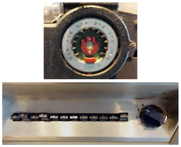
Control switches on the sorter select a numeric or zone sort. The photos below show these controls on the Type 80 (top) and 83 (bottom) sorters. The Type 80 sorter has a round commutator with tabs that are moved in or out to select which rows to use; the red tab selects a zone sort. The Type 83 sorter has pushbuttons to select rows, as well as a switch to select different types of sorting (Numeric, Zone, or Alpha).

Sorter controls on the Type 80 (top) and Type 83 (bottom) sorters.

Sorter controls on the Type 80 (top) and Type 83 (bottom) sorters.

A brief history of IBM's horizontal sorters

Type 80 sorter

In 1925, IBM introduced its first horizontal card sorter, the Type 80.[4] This sorter became very popular with 10,200 units in use by 1943. IBM continued to support this card sorter until 1980, a remarkable lifespan of 55 years.

IBM Type 80 punched card sorter.

IBM Type 80 punched card sorter.

The Type 80 sorter performed useful data processing with electromechanical technology without the benefits of transistors or even vacuum tubes. The Type 80 sorter used a relay to latch the electromagnet on for the duration of the card; this is the extent of its "intelligence".[5]

Even though it was electrically simple, the sorter was a piece of precision machinery. It sorted 450 cards per minute, so the chute blades must pop down and up more than 7 times per second. Any timing error could result in a mis-sorted card or could cause the blade to nick the edge of the card.

Type 82 sorter

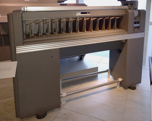
IBM's next sorter model was the Type 82, able to sort 650 cards per minute, and renting for 55 dollars per month. At the faster speed, an electromechanical relay wasn't fast enough to control the magnet, so vacuum tubes were used.

IBM Type 82 punched card sorter.

IBM Type 82 punched card sorter.

Type 83 sorter

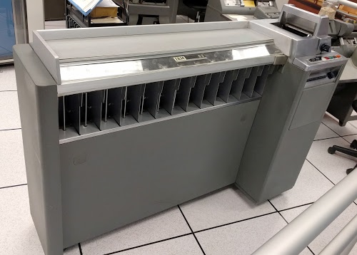
The next sorter model, the Type 83, was introduced in 1955. It could sort 1000 cards per minute and rented for 110 dollars per month. This sorter used a much more advanced technique for processing cards: instead of selecting the card chute at the instant a hole was detected, the 83 sorter read all the holes in the column before selecting a card chute. This allowed the Type 83 sorter to perform tasks that were impossible with the previous sorters, such as rejecting erroneous cards that had multiple holes in one column.

IBM Type 83 card sorter.

IBM Type 83 card sorter.

Type 84 sorter

IBM's most advanced sorter was the Type 84, introduced in 1959 and produced until 1978. This sorter replaced the wire brush with a photoelectric sensor and used solid state technology. A vacuum feed grabbed cards more effectively. With these improvements, it could process 2000 cards per minute, over 30 cards per second flying through the sorter.

IBM Type 84 card sorter. Photo courtesy of Computer History Museum.

IBM Type 84 card sorter. Photo courtesy of Computer History Museum.

Sorters and IBM's industrial design

As you may have noticed from the photos above, IBM's industrial design changed drastically from the early sorters.[6] The Type 80 sorter is an example of IBM's early hardware, built of cast iron in a "Queen Anne" style with curved cabriole legs. The mechanisms and motor of the Type 80 sorter are visible. By the time of the Type 82 sorter, IBM was using industrial design firms and had an "understated Art Deco aesthetic". Note the curved, sleek enclosure of the Type 82 sorter, and its shiny horizontal metal trim. The Type 83 and Type 84 sorters are more boxy, without the decorative trim, moving closer to the dramatic modernist style of IBM's computers of the 1960s.

The technology inside the sorter

This section looks inside the Type 83 sorter and describes how it was implemented using tube and relay technology. Unlike earlier sorters, the Type 83 sorter read the entire column before selecting the bin for the card. This permitted more complex processing, such as detecting erroneous cards with multiple punches. The sorter used 12 vacuum tubes to store the holes in the column as they were read. Electromechanical relays implemented the decision logic to select the bin, and then solenoids activated the chute blade for that bin.

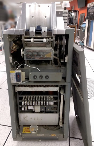
Removing the panel from the end of the sorter shows most of the mechanism (below). At the top is the feed hopper where cards are fed into the sorter. On the right, a pulley connects the feed mechanism to the motor. Mechanical cams (behind clear plastic) are also driven by the motor. Below the power switch and fuses, the 12 vacuum tubes are barely visible. Two rows of rectangular relays provide the control logic for the sorter. Behind the relay panel is the power supply for the sorter.

Inside the IBM type 83 card sorter. At top is the card feed. The cams are behind clear plastic.

Inside the IBM type 83 card sorter. At top is the card feed. The cams are behind clear plastic.

There is no clock for the sorter; all timing is relative to the position of the driveshaft, with one 360° rotation corresponding to one clock cycle. Sixteen cams (behind plastic near the top of the sorter) open and close switches at various points in the cycle to provide electrical signals at the right times.

The photo below shows the brush and the chute blade selection solenoids. On the right, you can see the pointer that indicates the selected column. The brush itself is below the pointer. In the middle are the 12 oblong coils that select the bin. These coils push the selected chute blades down (using the levers at the front), allowing the card to pass between the selected blades.

Brush and sort mechanism in the IBM type 83 card sorter.

Brush and sort mechanism in the IBM type 83 card sorter.

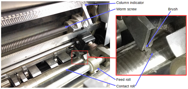
The card is read by a brush that makes electrical contact through a hole in the card. The brush is positioned to the proper column by manually turning a knob that rotates the worm screw and moves the brush. As you can see in the photo below, the small brush contacts the metal contact roll.

Brush mechanism in IBM Type 83 card sorter.

Brush mechanism in IBM Type 83 card sorter.

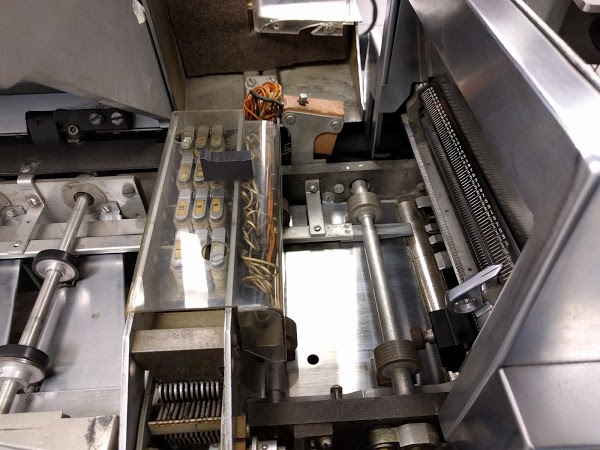
The photo below shows the drive rollers that feed cards through the sorter, dropping them into the appropriate bins, as directed by the chute blades. The chute blades are barely visible; they are the inch-wide metal strip on the right. The chute blades are stacked together, with just enough room for a card to pass between them.

Feed rollers and bins for the IBM type 83 card sorter. Cards enter at the far end. The chute blades are the inch-wide strip of metal to the right of the feed rolls.

Feed rollers and bins for the IBM type 83 card sorter. Cards enter at the far end. The chute blades are the inch-wide strip of metal to the right of the feed rolls.

In order to read a column before selecting a chute, the sorter needed a storage mechanism to remember the 12 hole values. This mechanism is an interesting combination of mechanical switches, vacuum tubes and relays.

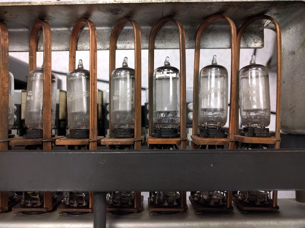
Type 2D21 thyratron tubes in the IBM Type 83 card sorter. Each tube stores the presence of one hole.

Type 2D21 thyratron tubes in the IBM Type 83 card sorter. Each tube stores the presence of one hole.

Each bit of storage used a 2D21 thyratron tube. This interesting tube is about 2 inches tall. Unlike a regular vacuum tube, it contains low-pressure xenon. If the tube is activated (via its two control grids), the xenon ionizes, causing the tube to remain on until current through it is interrupted. Thus, the tube can be used for storage. Each tube is in a pull-out module that has the necessary resistors at the bottom.

As each card row passes under the brush, the corresponding thyratron is selected. Rotating cams attached to the driveshaft mechanically activate switches at the right point in the cycle to select each thyratron.[7] It seems strange to combine high-speed tubes with mechanically operated switches, but cam-based timing was common in that era. Once the column has been read into the thyratron tubes, the hole pattern is transferred to relays for "processing".

Relay logic

Unlike the older sorters, the Type 83 sorter reads the entire column before selecting a bin. This lets it, for instance, reject erroneous cards with multiple punches in one column. How does it detect multiple punches? Instead of using logic gates built from tubes or transistors, it uses a network of relays. This section describes how relay logic works.

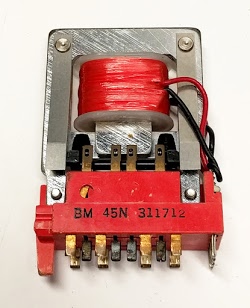
IBM relay (permissive make type).

IBM relay (permissive make type).

A relay (shown above) contains an electromagnet coil that moves contacts, switching circuits on or off like a toggle switch. In a typical relay, the circuit connects to the "normally closed" pin when the relay is inactive, and connects to the "normally opened" pin when the relay is active. A relay may have multiple sets of these contacts. The diagram below shows how a relay appears on IBM schematics. On the left is the electromagnet coil, and on the right is one set of contacts. The diagram shows the inactive state, with the center wire touching the bottom contact. When the relay is energized, the center wire moves and touches the top contact, switching the circuit.[8]

Symbol for a relay: relay number 9 and contact set 2.

Symbol for a relay: relay number 9 and contact set 2.

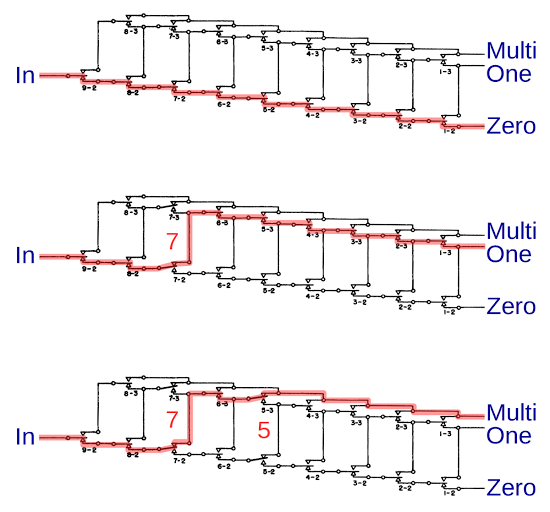
The diagram below shows the relay circuit in the sorter that counts the holes and determines if zero, one, or more holes are present. With no holes (top), current flows along the bottom path. A single hole (middle) energizes a relay (#7 in this case), transferring current to the middle path. The next hole (bottom) energizes a second relay (#5 in this case), transferring current to the top path. Thus, this chain of relays determines the number of holes present, and erroneous cards can be rejected.

Relay network in the IBM Type 83 card sorter. This circuit determines if the card has 0, 1, or more holes.

Relay network in the IBM Type 83 card sorter. This circuit determines if the card has 0, 1, or more holes.

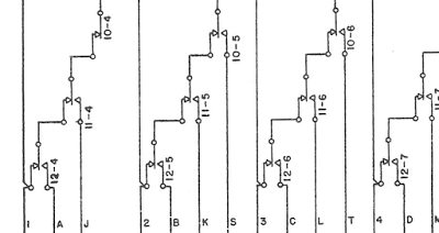
A more complex relay circuit was the optional faster alphabetic sorting feature available on the Type 83 sorter. For an additional $15 a month rental fee, customers could sort the most common letters in one pass, saving time while sorting. This circuit used several large relays, each with a dozen sets of contacts (an unusually large number). These relays decoded the hole pattern to determine the specific character and then selected the appropriate bin. The diagram below shows a small part of the circuit.

Relay network for enhanced alphabetic sorting in the IBM Type 83 card sorter.

Detail from relay network for enhanced alphabetic sorting in the IBM Type 83 card sorter.

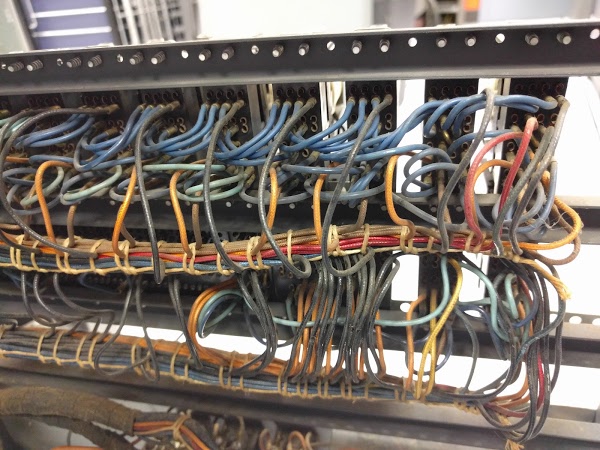
The photo below shows the wiring on the back of the relay panel. The wiring in the sorter is all point-to-point wiring, rather than printed circuit boards. Note that the wires are carefully laced into neat bundles.

Wiring inside the IBM type 83 card sorter. This is the back of the relay panel.

Wiring inside the IBM type 83 card sorter. This is the back of the relay panel.

The power supply

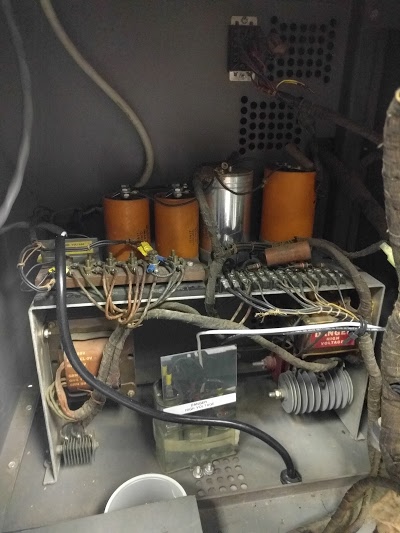
When the Type 80 sorter was introduced, standard AC power hadn't fully taken over and parts of the United States used DC or 25 Hertz AC.[9] Thus, the sorter needed to handle fifteen different line inputs including unusual ones such as 115V DC or 230V 25 Hertz AC. Internally, the sorter circuits used 115V DC, a rather high voltage for "logic" circuits. If the line voltage was AC, the power supply used a transformer and selenium rectifiers (an early form of diode build from stacks of selenium disks) to produce DC. The Type 81 power supply was considerably more complicated since its vacuum tubes required -40V DC. To create this voltage, the power supply used a vacuum tube oscillator, another transformer and vacuum tube diodes.

Power supply for the IBM Type 83 card sorter. Filter capacitors are at top. The power transformer is on the left. Selenium rectifiers (left and right) are built from stacks of selenium disks.

Power supply for the IBM Type 83 card sorter. Filter capacitors are at top. The power transformer is on the left. Selenium rectifiers (left and right) are built from stacks of selenium disks.

By the time the Type 83 sorter was introduced, AC line power was almost universal, so a transformer could replace the oscillator power supply. The picture above shows the power supply in a Type 83 sorter, showing the large power transformer (left), capacitors (orange cylinders), and selenium rectifiers (gray finned objects at lower left and right). Needless to say, modern switching power supplies are much more compact and efficient than the early power supplies used in the sorters.

Conclusion

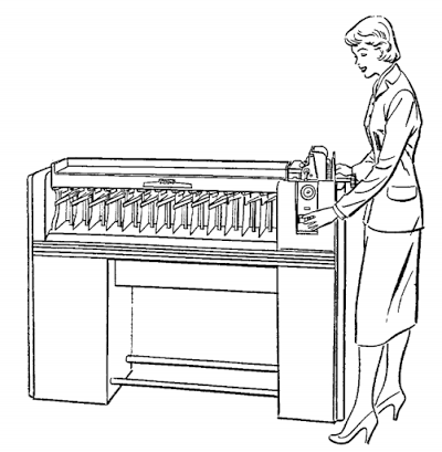
IBM Type 82 punched card sorter. From 'IBM Card Equipment Summary'.

IBM Type 82 punched card sorter. From IBM Card Equipment Summary, 1957.
Before computers existed, businesses carried out data processing tasks by using punched cards and electromechanical equipment such as the card sorter. Card sorters remained useful in the computer era and were still used until punched cards finally died out. Sorters used a variety of interesting technologies from mechanical brushes and cams to relay logic and thyristor tubes. Even though punched cards are now obsolete, their influence is visible whenever you use 80-column text.[5]

The Computer History Museum in Mountain View demonstrates a working card sorter weekly, so stop by if you're in the area. Thanks to the IBM 1401 restoration team and the Computer History Museum for access to the sorters.

If you're interested in vintage computing, you should follow me on Twitter.

Notes and references

[1] Herman Hollerith is one of the key inventors of the data processing industry. He founded a company that, after various mergers, became IBM in 1924. Hollerith's 1889 patent 395,782 (Art of Compiling Statistics) describes how to record data on punched cards and then generate statistics from those cards. Hollerith also gave his name to the Hollerith constants used for character data in old FORTRAN programs.

[2] Using a sorter to order cards for a report is roughly analogous to a database ORDER BY operation. Sorting cards so subtotals can be computed is analogous to a GROUP BY operation.

[3] Strictly speaking, radix sort on n records takes O(m*n) time if the field is m characters wide. But since punched cards limit m to 80 columns, m can be considered a constant factor, making radix sort linear.

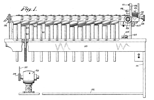
[4] The Type 80 card sorter was invented by Eugene Ford in 1925 and received patent 1,684,389 (Card feeding and handling device). The card sorter has many interesting features so it's a bit surprising that the patent covers just the "picker" that feeds cards through the sorter one at a time. The drawing below is from the patent, and can be compared with the photo of the sorter.

IBM card sorter, from patent 1,684,389.

IBM card sorter, from patent 1,684,389 (Card feeding and handling device), 1928.

You might wonder how the Type 80 card sorter was introduced in 1925 when the modern punched card was developed a few years later in 1928. The first Type 80 sorters worked with 45-column cards and were slightly modified in 1928 to support 80-column cards. The changes were minor since the cards remained the same size; the brush mechanism needed to have 80 stops instead of 45.

[5] For detailed information on the sorters (including wiring diagrams) see the Reference Manual and the IBM Customer Engineering Manual.

[6] The industrial design section is based on The Interface: IBM and the Transformation of Corporate Design. This book gives a detailed history and analysis of IBM's industrial design.

[7] A primitive but complex mechanism is used to select one thyratron tube as each row is read. Although the 12 thyratrons are physically installed in a line, they are electrically wired in a 3x4 grid. Four mechanical cams select a grid row; one cam is activated at a time. You'd expect three cams to select a grid column, but there are six. The problem is a single mechanical cam can't turn the switch on and off fast enough. The solution is to use two cams in series with staggered operation. The first cam closes the circuit to select the thyratron, while the second cam opens a short time later to de-select the thyratron. By using two cams and two switches, each switch has more time to open and close. As a card is read, the cams open and close, selecting each thyratron in sequence to hold the value (hole or no hole) for that card position. After the card column has been read into the thyratrons, the hole pattern is transferred to 12 relays and the thyratrons are reset for the next card.

[8] IBM's relays are discussed in detail in Commutation and Control, IBM Relays Reference Manual and IBM Relays Customer Engineering.

[9] The story of why parts of the US used 25 Hertz power instead of the standard 60 Hertz is interesting. Hydroelectric power was developed at Niagara Falls starting in 1886. To transmit power to Buffalo, Edison advocated DC, while Westinghouse pushed for polyphase AC. The plan in 1891 was to use DC for local distribution and (incredibly) compressed air to transmit power 20 miles to Buffalo, NY. By 1893, the power company decided to use AC, but used 25 Hertz due to the mechanical design of the turbines and various compromises. In 1919, more than two thirds of power generation in New York was 25 Hertz and it wasn't until as late as 1952 that Buffalo used more 60 Hertz power than 25 Hertz power. The last 25 Hertz generator at Niagara Falls was shut down in 2006. See 25-Hz at Niagara Falls, IEEE Power and Energy Magazine, Jan/Feb 2008 for details.
Reverse engineering the popular 555 timer chip (CMOS version)

This article explains how the LMC555 timer chip works, from the tiny transistors and resistors on the silicon chip, to the functional units such as comparators and current mirrors that make it work. The popular 555 timer integrated circuit is said to be the world's best-selling integrated circuit with billions sold since it was designed in 1970 by analog IC wizard Hans Camenzind[1]. The LMC555 is a low-power CMOS version of the 555; instead of the bipolar transistors in the classic 555 (which I described earlier), the CMOS chip is built from low-power MOS transistors. The LMC555 chip can be understood by carefully examining the die photo.

The structure of the integrated circuit

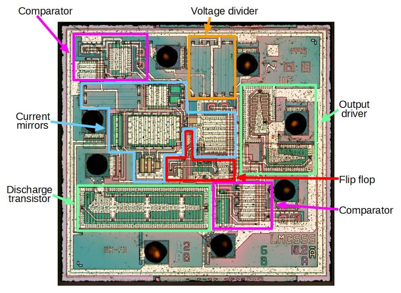
The photo below shows the silicon die of the LMC555 as seen through a microscope, with the main function blocks labeled (photo from Zeptobars). The die is very small, just over 1mm square. The large black circles are connections between the chip and its external pins. A thin layer of metal connects different parts of the chip. This metal is clearly visible in the photo as white lines and regions. The different types of silicon on the chip appear as different colors. Regions of the chip are treated (doped) with impurities to change the electrical properties of the silicon. N-type silicon has an excess of electrons (making it Negative), while P-type silicon lacks electrons (making it Positive). On top of the silicon, polysilicon wiring shows up as other colors. The silicon regions and polysilicon are the building blocks of the chip, forming transistors and resistors, which are connected by the metal layer.

Functional blocks in the LMC555 chip.

Functional blocks in the LMC555 chip.

A brief explanation of the 555 timer

The 555 chip is extremely versatile with hundreds of applications from a timer or latch to a voltage-controlled oscillator or modulator. To explain the chip, I will use one of the simplest circuits, an oscillator that cycles on and off at a fixed frequency.

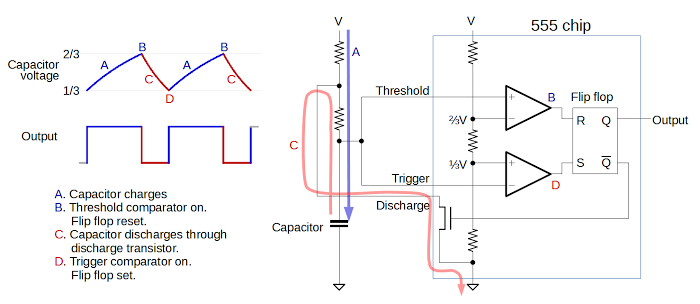
The diagram below illustrates the internal operation of the 555 timer used as an oscillator. An external capacitor is repeatedly charged and discharged to produce the oscillation. Inside the 555 chip, three resistors form a divider generating reference voltages of 1/3 and 2/3 of the supply voltage. The external capacitor will charge and discharge between these limits, producing an oscillation, as shown on the left. In more detail, the capacitor will slowly charge (A) through the external resistors until its voltage hits the 2/3 reference. At that point (B), the threshold (upper) comparator switches the flip flop off turning the output off. This turns on the discharge transistor, slowly discharging the capacitor (C) through the resistor. When the voltage on the capacitor hits the 1/3 reference (D), the trigger (lower) comparator turns on, setting the flip flop and the output on, and the cycle repeats. The values of the resistors and capacitor control the timing, from microseconds to hours.

Diagram showing how the 555 timer can operate as an oscillator.

Diagram showing how the 555 timer can operate as an oscillator.

To summarize, the key components inside the 555 timer are the comparators to detect the upper and lower voltage limits, the three-resistor divider to set these limits, the flip flop to keep track of whether the circuit is charging or discharging, and the discharge transistor. The 555 timer has two other pins (reset and control voltage) that I haven't covered above; they are used in more complex circuits.

Transistors inside the IC

Like most integrated circuits, the CMOS 555 timer chip is built from two types of transistors, PMOS and NMOS. In contrast, the classic 555 timer uses the older technology of bipolar transistors (NPN and PNP). CMOS is popular because it uses much less power than bipolar. CMOS transistors be packed into a chip very densely without overheating, which is why CMOS has ruled the microprocessor market since the 1980s. Although the 555 doesn't require many transistors, low power consumption is still an advantage.

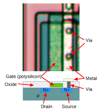
The diagram below shows an NMOS transistor in the chip, with a cross section below. Since the transistor is built from overlapping layers, the die photo is a bit tricky to understand, but the cross section should help clarify it. The different colors in the silicon indicate regions that has been doped to form N and P regions. The green rectangle is polysilicon, a layer above the silicon. The whitish rectangle is the metal layer on top. The vias are connections between the layers.

The structure of an NMOS transistor in the LMC5555 CMOS timer chip.

The structure of an NMOS transistor in the LMC5555 CMOS timer chip.

A MOS transistor can be thought of as a switch that connects or disconnects the source and drain, based on the voltage on the gate. The transistor consists of two rectangular strips of silicon that has been doped negative (N), embedded in the underlying P silicon. The gate consists of a layer of conductive polysilicon above and between the drain and source. The gate is separated from the underlying silicon by a very thin layer of insulating oxide. If voltage is applied to the gate, it produces an electric field that changes the properties of the silicon below the gate, allowing current to flow.[2] The photo also shows the metal connection to the source, along with the "vias" that connect the silicon layer to the metal layer through the insulating oxide.[3]

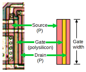
The second type of transistor is PMOS, shown below. PMOS transistors are opposite to NMOS in many ways; they are called complementary, which is the C in CMOS. PMOS uses a source and drain of P-doped silicon embedded in N-doped silicon. The transistor is turned on by a low voltage on the gate (opposite to NMOS), causing current to flow from the source to drain. The metal connections to the source, gate, and drain are visible below, with circular vias to the underlying layers. (Note that the diagram on the right is not a cross section, but a simplified "overhead" view.) In the die photo, NMOS transistors are blue with a green gate, while PMOS transistors are pink with orange gates. These colors are created by interference due to the thickness of the layers, and saturation is enhanced in the photo.

Die photo of a PMOS transistor in the LMC555 timer. A simplified diagram of the transistor is on the right.

Die photo of a PMOS transistor in the LMC555 timer. A simplified diagram of the transistor is on the right.

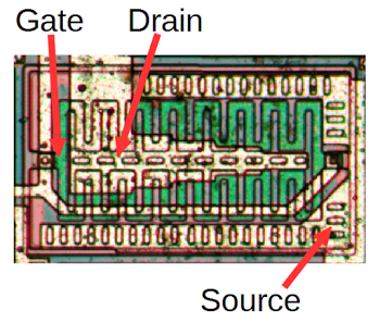
The output transistors in the 555 are much larger than the other transistors and have a different structure in order to produce the high-current output. The photo below shows one of the output transistors. Note the zig-zag structure of the gate, between the source (outside) and drain (center). Also note that the metal layer for the drain is narrow on the right and widens as it exits the transistor in order to handle the increasing current.[4]

A large NMOS output transistor in the LMC555 CMOS timer chip.

A large NMOS output transistor in the LMC555 CMOS timer chip.

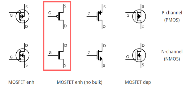
A variety of symbols are used to represent MOS transistors in schematics; the diagram below shows some of them. In this article, I use the highlighted symbols.
Various symbols used for MOS transistors. From Wikipedia.
Various symbols used for MOS transistors. Based on Wikipedia.

How resistors are implemented in silicon

Resistors are a key component of analog circuits. Unfortunately, resistors in ICs are large and inaccurate; the resistances can vary by 50% from chip to chip. Thus, analog ICs are designed so only the ratio of resistors matters, not the absolute values, since the ratios remain nearly constant even if the values vary depending on manufacturing conditions.

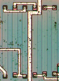
These resistors form the voltage divider in the CMOS 555 timer.

These resistors form the voltage divider in the CMOS 555 timer.

The photo above shows the resistors that form the voltage divider in the chip. There are six 50kΩ resistors, connected in series to form three 100kΩ resistors. The resistors are the pale vertical rectangles. At the end of each resistor, a via and P+ silicon well (pink square) connects the resistor to the metal layer, which wires them together. The resistors themselves are probably P-doped silicon.

To reduce current, the CMOS chip uses 100kΩ resistors, much larger than the 5kΩ resistors in the bipolar 555 timer. Urban legend says that the 555 is named after these three 5K resistors, but according to its designer 555 is just an arbitrary number in the 500 chip series

IC component: The current mirror

There are some subcircuits that are very common in analog ICs, but may seem mysterious at first. The current mirror is one of these. If you've looked at analog IC block diagrams, you may have seen the symbols below, indicating a current source, and wondered what a current source is and why you'd use one.

Schematic symbols for a current source.

Schematic symbols for a current source.

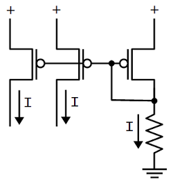
The idea of the current mirror is you start with one known current and then you can "clone" multiple copies of the current with a simple transistor circuit, the current mirror. A common use of a current mirror is to replace resistors. As explained earlier, resistors inside ICs are both inconveniently large and inaccurate. It saves space to use a current mirror instead of a resistor whenever possible. Also, the currents produced by a current mirror are nearly identical, unlike the currents produced by two resistors.

The circuit below shows how a current mirror is implemented with three identical transistors.[5] A reference current passes through the transistor on the right. (In this case, the current is set by the resistor.) Since all the transistors have the same emitter voltage and base voltage, they source the same current, so the currents on the left match the reference current on the right. For more flexibility, you can modify the relative sizes of the transistors in the current mirror and make the copied current larger or smaller than the reference current.[4] The CMOS 555 chip uses a variety of transistor sizes to control the currents in the circuit.

A current mirror formed from PMOS transistors. The left two currents mirror the current on the right, which is controlled by the resistor.

A current mirror formed from PMOS transistors. The left two currents mirror the current on the right, which is controlled by the resistor.

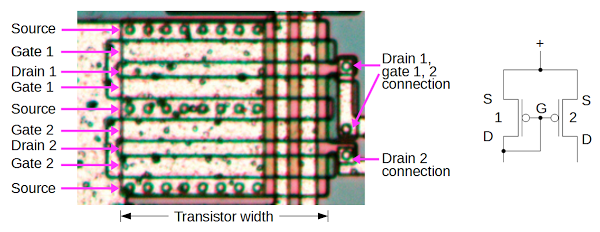
The diagram below shows one of the current mirrors in the LMC555 chip, formed from two transistors. Each transistor is actually two transistors in parallel, which is a common trick in the chip, so there are physically two pairs of transistors. It's a bit tricky to see the transistors because the metal layer partially covers them, but hopefully the description will make sense. Starting at the top, the first transistor is formed from the wide rectangles for source, gate 1, and drain 1. Note the vias connecting the metal layer to the source. The next transistor shares drain 1, with the second gate 1 and source below. Since these two transistors share the drain, and the sources and gates are wired the same, the two transistors effectively form one larger transistor. Likewise, there are two transistors below in parallel: source, gate 2, drain 2, and then drain2, gate2, source.

Two pairs of PMOS transistors in the LMC555 chip form a current mirror.

Two pairs of PMOS transistors in the LMC555 chip form a current mirror.

The schematic on the right shows how the transistors are wired together as a current mirror. If you look at the photo carefully, you can see that a single polysilicon strip snakes back and forth to form all the gates, so the gates are connected together. On the right, the upper metal strip connects drain 1 and the gates to the rest of the circuit. The lower metal strip is connected to drain 2.

IC component: The differential pair

The second important circuit to understand is the differential pair, the most common two-transistor subcircuit used in analog ICs.[6] You may have wondered how a comparator compares two voltages, or an op amp subtracts two voltages. This is the job of the differential pair.

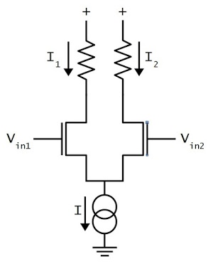
Schematic of a simple differential pair circuit. The current sink sends a fixed current I through the differential pair. If the two inputs are equal, the current is split equally between the two branches. Otherwise, the branch with the higher input voltage gets most of the current.

Schematic of a simple differential pair circuit. The current sink sends a fixed current I through the differential pair. If the two inputs are equal, the current is split equally between the two branches. Otherwise, the branch with the higher input voltage gets most of the current.

The schematic above shows a simple differential pair. The current source at the bottom sinks a fixed current I, which is split between the two input transistors. If the input voltages are equal, the current will be split equally into the two branches (I1 and I2). If one of the input voltages is a bit higher than the other, the corresponding transistor will conduct more current, so one branch gets more current and the other branch gets less. A small input difference is enough to direct most of the current into the "winning" branch, flipping the comparator on or off. Rather than resistors, the chip uses a current mirror on the two branches. This acts as an active load and increases the amplification.

Inverters and the flip flop

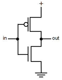
Although the 555 is an analog circuit, it contains a digital flip flop to remember its state. The flip flop is built out of inverters, simple logic circuits that turn a 1 into a 0 and vice versa. The 555 uses standard CMOS inverters, as shown below.

Structure of a CMOS inverter: a PMOS transistor at top and a NMOS transistor at bottom.

Structure of a CMOS inverter: a PMOS transistor at top and a NMOS transistor at bottom.

The inverter is built from two transistors. If the input is 0 (i.e. low), the PMOS transistor on top turns on, connecting the positive supply to the output, producing a 1. If the input is 1 (high), the NMOS transistor on the bottom turns on, connecting ground to the output, producing a 0. The magical part of CMOS is that the circuit uses almost no power. Current doesn't flow through the gate (because of the insulating oxide layer), so the only power usage is a tiny pulse when the output changes state, to charge or discharge the wire's capacitance.[7]

The diagram below shows the circuit for the flip flop. Two inverters are connected in a loop to form a latch. If the top inverter outputs 1, the bottom outputs 0, forming a stable cycle. If the top inverter outputs 0, the bottom outputs 1, again forming a stable cycle.

Circuit diagram of the flip flop in the LMC555 CMOS timer chip.

Circuit diagram of the flip flop in the LMC555 CMOS timer chip.

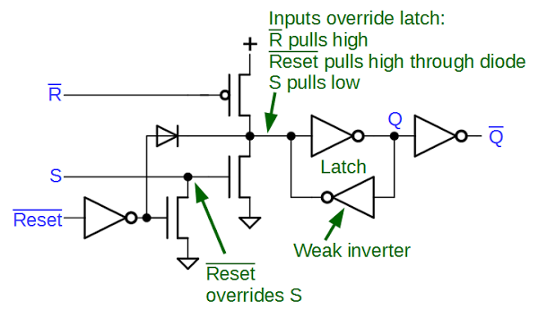
To change the value stored in the flip flop, the new value is simply forced into the latch, overriding the existing value with brute force. To make this work, the bottom inverter is "weak", using low-current transistors. This allows the set or reset inputs to overpower the weak inverter and the latch will immediately flip into the proper state The R (reset) and S (set) inputs come from the comparators and pull the latch input high or low through the transistors. Reset comes from the input pin and pulls the latch input high through a diode; the Reset inverter's output current is controlled by a current mirror. Reset will pull S low, blocking the action of a contradictory S input.

The 555 schematic interactive explorer

The 555 die photo and schematic below are interactive. Click on a component in the die or schematic, and a brief explanation of the component will be displayed. (For a thorough discussion of how the 555 timer works, see 555 Principles of Operation.)

For a quick overview, the large output transistors and discharge transistor are distinguishable by their zig-zag gate pattern. The current mirror transistors are generally large. The threshold comparator consists of Q1 through Q5. The trigger comparator consists of Q13 through Q18. Q19 through Q29 form the flip flop circuit. The voltage divider resistors are in the upper center of the chip.[8]

Click the die or schematic for details...

I created the above schematic by reverse-engineering the chip, so I don't guarantee full correctness. A PDF of my schematic is here and a differently-formatted version is here. The schematic of a different CMOS 555 is here, and it's interesting to compare the differences. While the comparators are the same, the current mirrors are built differently, and the flip flop circuit is very different.

CMOS 555 compared with traditional bipolar 555

The regular 555 timer was designed in 1970, while a CMOS version (the ICM7555) wasn't released until 1978. The LMC555 described in this article came out around 1988, while the die itself has a date of 1996.

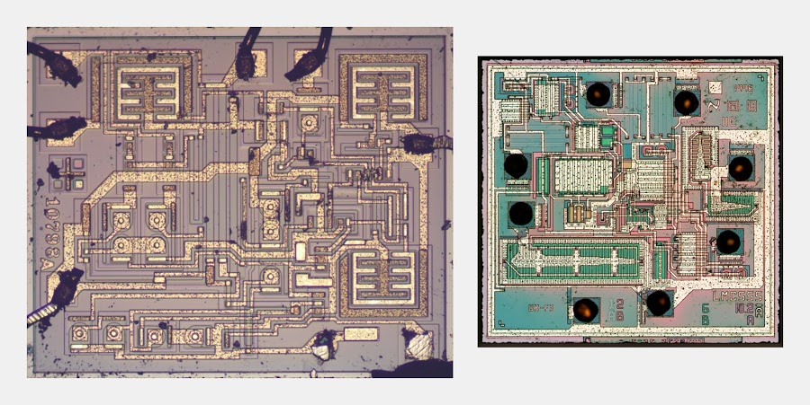
The image below compares the classic 555 timer (left) with the CMOS LMC555 (right), both to the same scale. While the bipolar chip is constructed from silicon connected by a metal layer, the CMOS chip has an additional interconnect layer of polysilicon, which makes the chip more complex to understand visually. The CMOS chip is smaller. In addition, the CMOS chip has a lot of wasted space in the bottom and upper right, so it could have been made even smaller. The CMOS transistors are much more complex than the bipolar transistors. Except for the output transistors, the bipolar transistors are all simple individual units. Most of the CMOS transistors in comparison are built from two or more transistors in parallel. The classic 555 uses many more resistors than the CMOS 555; 16 versus 4.

Die photos of the 555 timer (left) and CMOS 555 timer (right), to the same scale.

Die photos of the 555 timer (left) and CMOS 555 timer (right), to the same scale.

You can see from the photo that the features are smaller in the CMOS chip. The smallest lines in the regular 555 are 10-15µm, while the CMOS chip has 6µm features. Advanced chips in 1996 used the 350nm process (about 17 times smaller), so the LMC555 was nowhere near the cutting edge of CMOS technology.

Comparing these chips illustrates the power consumption benefits of CMOS. The standard 555 timer typically uses 3 mA of current, while this CMOS version only uses 100µA (and other versions use below 5µA). An input to the 555 can draw .5µA, while an input to the CMOS version uses an incredibly small 10pA, more than four orders of magnitude smaller. The smaller input "leakage" currents permit much longer delays with the CMOS chips.[9]

Conclusion

At first, a chip die photo seems too complex to understand. But a careful look at the die of the LMC555 CMOS timer chip reveals the components that make up the circuit. One can pick out the PMOS and NMOS transistors, see how they are combined into circuits, and understand how the chip operates. Because the CMOS chip has a layer of polysilicon that isn't present in the classic bipolar 555 chip, it takes more effort to understand the CMOS chip. But fundamentally, both chips use similar analog functional blocks: the current mirror and the differential pair.

If you've found this look at the CMOS version of the 555 chip interesting, you should also look at my teardown of the classic 555 chip. Thanks to Zeptobars for the die photo of the CMOS chip.

Get announcements of my new articles by following @kenshirriff on Twitter.

Notes and references

[1] The book Designing Analog Chips written by the 555's inventor Hans Camenzind is really interesting, and I recommend it if you want to know how analog chips work. Chapter 11 has an extensive discussion of the 555's history and operation. Page 11-3 claims the 555 has been the best-selling IC every year, although I don't know if that is still true — microcontrollers have replaced timers in many circuits. The free PDF is here or get the book.

[2] The structure of a MOSFET transistor explains several things about it. The transistor is called a "field-effect transistor" (FET) because it is controlled by the electric field on the gate. Because the gate is separated by an insulating oxide layer, there is essentially no current flow through the gate. This is why CMOS circuits have such low power consumption. The thin oxide layer, however, can easily be damaged or destroyed by static electricity, which is why MOS integrated circuits are sensitive to static electricity.

[3] For simplicity, the cross-section diagram doesn't show the highly-doped P region (pink) that provides a connection to the underlying P body silicon, keeping it at the right voltage. (A via between the metal layer and pink silicon region is visible at the top of the diagram.) MOS transistors typically connect the source and body silicon together; the source and drain are otherwise structurally the same. I should also mention that the cross-section is simplified; in a real chip, the layers are more irregular.

MOS transistors originally used metal for the gate so they were named MOS after the three layers: Metal, Oxide, and Semiconductor (silicon). Although polysilicon gates replaced metal gates since the 1970s, the name remains MOS even though POS would be more accurate. Federico Faggin (a developer of the 4004 and Z-80 processors) explains how silicon gate technology revolutionized chips here.

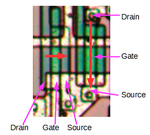
[4] The structure of the transistor controls how much current flows through it. In particular, the current is proportional to the ratio of the gate's width and length (W/L). It's straightforward to see that doubling the width of the gate is similar to putting two transistors side-by-side in parallel, allowing twice the current. Doubling the length of the gate (so the current needs to travel twice as far through the gate) cuts the current in half due to physics reasons.

Two NMOS transistors in the LMC555 chip's flip flop. The left transistor is typical. The right transistor is a weak transistor with current flowing top to bottom.

Two NMOS transistors in the LMC555 chip's flip flop. The left transistor is typical. The right transistor is a weak transistor with current flowing top to bottom.

In the CMOS 555 chip, transistors have a wide variety of W/L ratios, especially to control the currents in different branches of the current mirrors. Some of the weak transistors are hard to spot, such as the above weak transistor from the flip flop. The transistor on the left has a W/L ratio of about 7. The transistor on the right looks almost identical but careful examination shows it is actually rotated 90 degrees with the source and drain arranged vertically rather than horizontally. The W/L ratio of the transistor on the right is only about 0.17, making the transistor about 40 times weaker than the one one the left. In other words, the transistor on the left has a wide, short gate while the transistor on the right has a narrow, long gate.

[5] For more information about current mirrors, check wikipedia, any analog IC book, or chapter 3 of Designing Analog Chips.

[6] Differential pairs are also called long-tailed pairs. According to Analysis and Design of Analog Integrated Circuits the differential pair is "perhaps the most widely used two-transistor subcircuits in monolithic analog circuits." (p214) For more information about differential pairs, see wikipedia, any analog IC book, or chapter 4 of Designing Analog Chips.

[7] Because CMOS only uses power when circuits change state, power consumption is roughly proportional to frequency. This is the main limitation for CPU clock frequency: the chip will overheat if it is clocked too fast.

[8] Note that the three resistors for the voltage divider are parallel and next to each other. This helps ensure they have the same resistance even if there are electrical variations across the silicon.

[9] If you want a 555 timer that provides a long delay up to days, the CSS555 is an unusual option. This chip is pin-compatible with the 555, but internally it includes a programmable counter that can divide the output up to 1 million. The chip contains a one-byte EEPROM to hold the configuration and is programmed serially via the trigger and reset pins. Once programmed, it acts just like a regular 555, except with a very long delay.

Counterfeit Macbook charger teardown: convincing outside but dangerous inside

What's inside a counterfeit Macbook charger? After my Macbook charger teardown, a reader sent me a charger he suspected was counterfeit. From the outside, this charger is almost a perfect match for an Apple charger, but disassembling the charger shows that it is very different on the inside. It has a much simpler design that lacks quality features of the genuine charger, and has major safety defects.

Inside a counterfeit MagSafe 45W charger.

Inside a counterfeit MagSafe 45W charger.

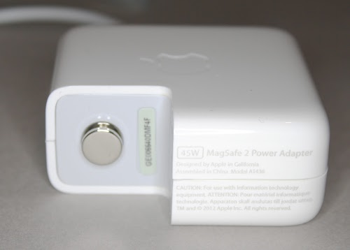
The counterfeit Apple chargers I've seen in the past have usually had external flaws that give them away, but this charger could have fooled me. The exterior text on this charger was correct, no "Designed by Abble" or "Designed by California". It had a metal ground pin, which fakes often exclude. It had the embossed Apple logo on the case. The charger isn't suspiciously lightweight. Since I've written about these errors in fake chargers before, I half wonder if the builders learned from my previous articles. One minor flaw is the serial number sticker (to the right of the ground pin) was a bit crooked and not stuck on well.

This counterfeit MagSafe 45W charger has the same 'Designed by Apple in California' text as the genuine charger. Unlike many fakes, it has a metal ground pin (although it isn't connected internally). To the right of the ground pin, the serial number label is a bit crooked, which is a hint that something isn't right.

This counterfeit MagSafe 45W charger has the same 'Designed by Apple in California' text as the genuine charger. Unlike many fakes, it has a metal ground pin (although it isn't connected internally). To the right of the ground pin, the serial number label is a bit crooked, which is a hint that something isn't right.

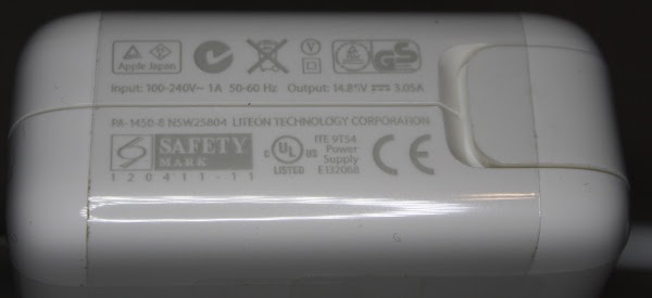
The photo below shows the safety certifications that the charger claims to have. Again, it looks genuine, with no typos or ugly fonts.

The counterfeit power supply has all the same safety indications as a real power supply.

The counterfeit power supply has all the same safety indications as a real power supply.

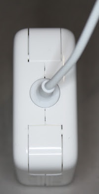
One flaw that made the original purchaser suspicious was the quality of the case didn't seem up to Apple standards. It didn't feel quite like his old charger when tapped, and the joints appear slightly asymmetrical, as you can see in the picture below.

The seams in a counterfeit Magsafe power supply are a bit asymmetrical.

The seams in a counterfeit Magsafe power supply are a bit asymmetrical.

A problem showed up when I plugged in the charger and measured the output at the Magsafe connector. I measured 14.75 volts output and got a spark when I shorted the pins. Since the charger is rated at 14.85 volts, this may seem normal, but the behavior of a real charger is different. A Magsafe charger initially produces a low-current output of 3 to 6 volts, so shorting the output should not produce a spark. Only when a microcontroller inside the charger detects that the charger is connected to a laptop does the charger switch to the full output power. (Details are in my Magsafe connector teardown article.) This is a safety feature of the real charger that reduces the risk from a short circuit across the pins. The counterfeit charger, on the other hand, omits the microcontroller circuit and simply outputs the full voltage at all times. This raises the risk of burning out your laptop if you plug the connector in crooked or metallic debris sticks to the magnet.

Inside the charger

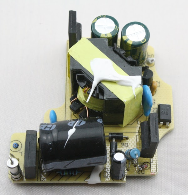
Cracking the charger open with a chisel reveals the internal circuitry. A real Apple charger is packed full of complex circuitry, while this charger had a fairly low density board that implemented a simple flyback switching power supply.

A view of the counterfeit MagSafe charger with the case and heat sink removed.

A view of the counterfeit MagSafe charger with the case and heat sink removed.

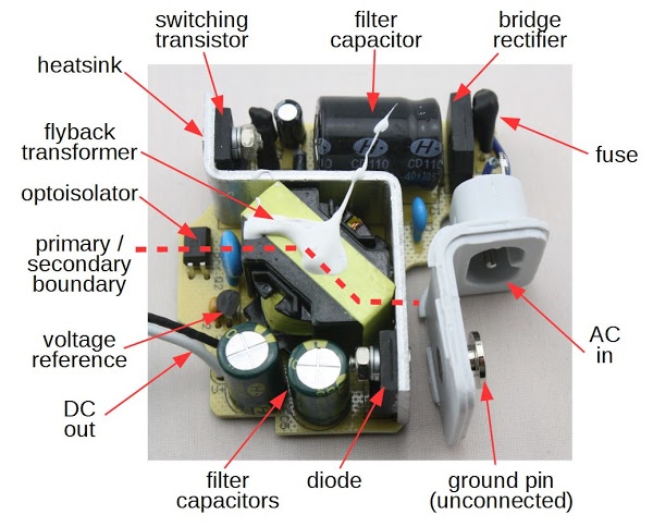
The circuit is a fairly standard flyback power supply. To understand how it works, look at the diagram below, going counterclockwise from the AC input on the right. After going through a fuse, the power is converted to DC by a bridge rectifier. The large filter capacitor smooths out the DC. Next, the switching transistor chops the DC into pulses, which are fed into the flyback transformer. The transformer's low-voltage output is converted back to DC by the output diode. The output filter capacitors smooth the DC output.

The counterfeit Magsafe power supply uses a standard flyback switching power supply circuit. AC enters at the right and is converted to DC. The switching transistor sends pulses into the flyback transformer (center), which produces the low voltage output (left).

The counterfeit Magsafe power supply uses a standard flyback switching power supply circuit. AC enters at the right and is converted to DC. The switching transistor sends pulses into the flyback transformer (center), which produces the low voltage output (left).

A TL431A voltage reference generates a feedback signal from the output, which is fed to the control IC through the optoisolator. While this circuit may seem complex, it's pretty standard for a simple charger. A genuine Macbook charger on the other hand has a much more complex circuit, as I describe in my teardown.

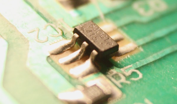
The charger is controlled by a tiny 6-pin IC on the underside of the board. It switches the MOSFET on and off at the proper rate (about 60 kilohertz) to generate the desired output voltage. The control IC is labeled "63G01 415", but I couldn't find any chip that matches that description. (Update: a clever reader identified the chip as the OB2263.)

Closeup of the tiny control IC inside a counterfeit MagSafe 45W power supply.

Closeup of the tiny control IC inside a counterfeit MagSafe 45W power supply.

What's wrong with this charger

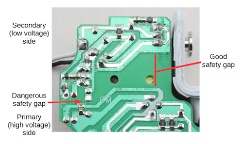
The most important feature of a charger is the isolation between the potentially-dangerous AC input and the low-voltage output. High voltage and low voltage should be separated by a safety gap of at least 4mm (to simplify the UL's creepage and clearance rules). On the circuit board below, the high voltage input section is at the bottom and the low voltage output section is at the top. On the right half of the board, the two sections are separated by a large gap, which is good. On the left, there should be a gap (bridged by the optoisolator). Unfortunately, traces and components pass through this area making the gap dangerously small, under 1 mm. Any moisture or loose solder could bridge this gap sending high voltage to the output.

The counterfeit MagSafe charger has a dangerously small distance between the low voltage side (top) and the high voltage side (bottom). This is why you shouldn't buy counterfeit chargers.

The counterfeit MagSafe charger has a dangerously small distance between the low voltage side (top) and the high voltage side (bottom). This is why you shouldn't buy counterfeit chargers.

I'm puzzled as to why counterfeit chargers never manage to have sufficient clearance distances. They use simple, low-complexity circuits so the circuit board layout should be straightforward. Except in the smallest cube phone chargers, they aren't fighting for every millimeter of space. It shouldn't take much additional effort to make the boards safer.

The second safety flaw is the heat sink that provides cooling for the input-side MOSFET and the output-side diode. The heat sink is basically a giant conductor between the two sides of the circuit, with only small gaps separating it from active parts of the circuit.

As well as having large creepage and clearance distances between high and low voltages, genuine chargers also make extensive use of insulating tape for separation. The counterfeit charger lacks extra insulation, except heat-shrink tubing around the fuse and fusible resistor. I didn't disassemble the transformer, but I expect it also lacks the necessary insulation.

The counterfeit charger has a metal ground pin (unlike other fakes I've seen that have a plastic pin). However, the pin is just for appearance and is not connected to anything.

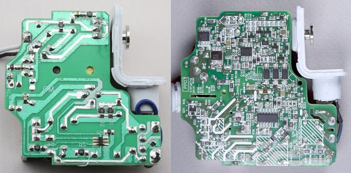
The photo below compares the underside of the counterfeit 45W charger (left) with a genuine Apple 60W charger (right). As you can see, the counterfeit has a simple circuit board with just a few parts, while the genuine charger is crammed full of parts. The two boards are in totally different worlds of design complexity. The additional parts provide better power quality and improved safety in the real charger; this is part of the reason genuine chargers are significantly more expensive.

Comparison of a counterfeit MagSafe 45W charger (left) and a genuine 60W charger (right). The genuine charger is crammed full of components, while the counterfeit just has a few components.

Comparison of a counterfeit MagSafe 45W charger (left) and a genuine 60W charger (right). The genuine charger is crammed full of components, while the counterfeit just has a few components.

Quality of the power

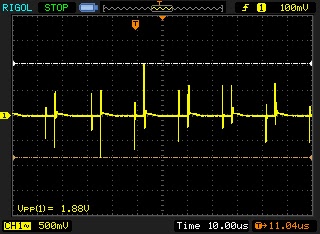
I measured the output power from the counterfeit charger with an oscilloscope, while drawing 15 watts. As you can see below, the output power is not smooth, but has pairs of large spikes when the switching transistor turns on and off. The charger operates at a frequency of about 60 kilohertz. More filtering inside the charger reduces these voltage spikes, but would cost more.

The switching power supply operates at about 60 kilohertz, producing large voltage spikes in the output. You can see a spike when the transistor switches on, followed by another spike when it switches off.

The switching power supply operates at about 60 kilohertz, producing large voltage spikes in the output. You can see a spike when the transistor switches on, followed by another spike when it switches off.
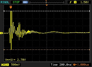
The oscilloscope trace below zooms in on one of the spikes. You can see that the spike measures 2.7 volts peak-to-peak, which is a lot of noise to be feeding into your laptop.

The output of the counterfeit charger has large 2.7V noise spikes when a transistor switches internall.

The output of the counterfeit charger has large 2.7V noise spikes when a transistor switches internally.

Conclusion

This counterfeit Magsafe charger is convincing from the outside, with more attention to detail than most. Until I opened it up, I wasn't completely sure that it was counterfeit. But on the inside, the difference between the counterfeit and real chargers is clear. The counterfeit has a much simpler circuit that provides poorer-quality power. It also ignores safety requirements with less than a millimeter separating you and your computer from a dangerous shock. While counterfeit chargers are much cheaper, they are also dangerous to you and your computer. Thanks to Richard S. for providing the charger.

I've written a bunch of articles before about chargers, so if this article seems familiar, you're probably thinking of an earlier article, such as: Magsafe charger teardown, iPhone charger teardown or iPad charger teardown.

You can follow me on Twitter and find out about my new articles.

Notes

For those who care about the component details, the MOSFET is a 600V, 7.5A transistor from Fairchild (FQPF8N60C datasheet). The optoisolator is a Kento JC817 (datasheet). The output diode is a NAMC MBRF10100CT 10A 100V Schottky barrier rectifier. I was unable to identify the control IC, which is marked with "63GO1 415". The Y capacitor (blue) is JNC JN472M 250V 4.7nF capacitor.