Could an IBM mainframe from the 1960s mine Bitcoin? The idea seemed crazy, so I decided to find out. I implemented the Bitcoin hash algorithm in assembly code for the IBM 1401 and tested it on a working vintage mainframe. It turns out that this computer could mine, but so slowly it would take more than the lifetime of the universe to successfully mine a block. While modern hardware can compute billions of hashes per second, the 1401 takes 80 seconds to compute a single hash. This illustrates the improvement of computer performance in the past decades, most famously described by Moore's Law.
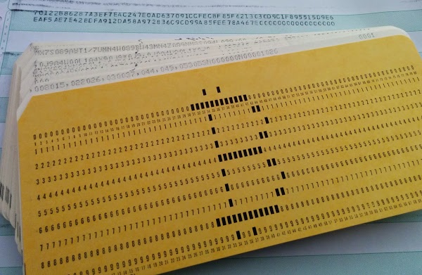
The photo below shows the card deck I used, along with the output of my SHA-256 hash program as printed by the line printer. (The card on the front of the deck is just for decoration; it was a huge pain to punch.) Note that the second line of output ends with a bunch of zeros; this indicates a successful hash.
Card deck used to compute SHA-256 hashes on IBM 1401 mainframe. Behind the card deck is the line printer output showing the input to the algorithm and the resulting hash.
How Bitcoin mining works
Bitcoin, a digital currency that can be transmitted across the Internet, has attracted a lot of attention lately. If you're not familiar with how it works, the Bitcoin system can be thought of as a ledger that keeps track of who owns which bitcoins, and allows them to be transferred from one person to another. The interesting thing about Bitcoin is there's no central machine or authority keeping track of things. Instead, the records are spread across thousands of machines on the Internet.
The difficult problem with a distributed system like this is how to ensure everyone agrees on the records, so everyone agrees if a transaction is valid, even in the presence of malicious users and slow networks.
The solution in Bitcoin is a process called mining—about every 10 minutes a block of outstanding transactions is mined, which makes the block official.
To prevent anyone from controlling which transactions are mined, the mining process is very difficult and competitive.
In particular a key idea of Bitcoin is that mining is made very, very difficult, a technique called proof-of-work. It takes an insanely huge amount of computational effort to mine a block, but once a block has been mined, it is easy for peers on the network to verify that a block has been successfully mined. The difficulty of mining keeps anyone from maliciously taking over Bitcoin, and the ease of checking that a block has been mined lets users know which transactions are official.
As a side-effect, mining adds new bitcoins to the system. For each block mined, miners currently get 25 new bitcoins (currently worth about $6,000), which encourages miners to do the hard work of mining blocks. With the possibility of receiving $6,000 every 10 minutes, there is a lot of money in mining and people invest huge sums in mining hardware.
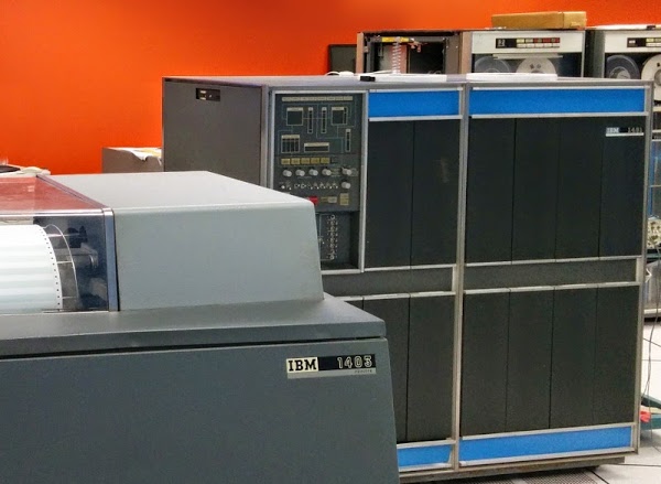
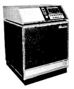
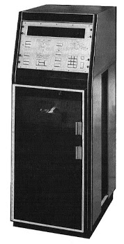
Line printer and IBM 1401 mainframe at the Computer History Museum. This is the computer I used to run my program. The console is in the upper left. Each of the dark rectangular panels on the computer is a "gate" that can be folded out for maintenance.
Mining requires a task that is very difficult to perform, but easy to verify. Bitcoin mining uses cryptography, with a hash function called double SHA-256. A hash takes a chunk of data as input and shrinks it down into a smaller hash value (in this case 256 bits). With a cryptographic hash, there's no way to get a hash value you want without trying a whole lot of inputs. But once you find an input that gives the value you want, it's easy for anyone to verify the hash. Thus, cryptographic hashing becomes a good way to implement the Bitcoin "proof-of-work".
In more detail, to mine a block, you first collect the new transactions into a block. Then you hash the block to form an (effectively random) block hash value. If the hash starts with 16 zeros, the block is successfully mined and is sent into the Bitcoin network. Most of the time the hash isn't successful, so you modify the block slightly and try again, over and over billions of times. About every 10 minutes someone will successfully mine a block, and the process starts over. It's kind of like a lottery, where miners keep trying until someone "wins". It's hard to visualize just how difficult the hashing process is: finding a valid hash is less likely than finding a single grain of sand out of all the sand on Earth. To find these hashes, miners have datacenters full of specialized hardware to do this mining.
Next, I'll discuss the hash function used in Bitcoin, which is based on a standard cryptographic hash function called SHA-256.
Bitcoin uses "double SHA-256" which simply applies the SHA-256 function twice.
The SHA-256 algorithm is so simple you can literally do it by hand, but it manages to scramble the data entirely unpredictably.
The algorithm takes input blocks of 64 bytes, combines the data cryptographically, and generates a 256-bit (32 byte) output.
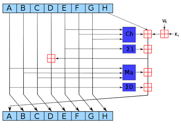
The algorithm uses a simple round and repeats it 64 times. The diagram below shows one round, which takes eight 4-byte inputs, A through H, performs a few operations, and generates new values for A through H.
The dark blue boxes mix up the values in non-linear ways that are hard to analyze cryptographically.
(If you could figure out a mathematical shortcut to generate successful hashes, you could take over Bitcoin mining.)
The Ch "choose" box chooses bits from F or G, based on the value of input E.
The Σ "sum" boxes rotate the bits of A (or E) to form three rotated versions, and then sums them together modulo 2.
The Ma "majority" box looks at the bits in each position of A, B, and C, and selects 0 or 1, whichever value is in the majority.
The red boxes perform 32-bit addition, generating new values for A and E.
The input Wt is based on the input data, slightly processed. (This is where the input block gets fed into the algorithm.)
The input Kt is a constant defined for each round.
As can be seen from the diagram above, only A and E are changed in a round. The other values pass through unchanged, with the old A value becoming the new B value, the old B value becoming the new C value and so forth.
Although each round of SHA-256 doesn't change the data much, after 64 rounds the input data will be completely scrambled, generating the unpredictable hash output.
The IBM 1401
I decided to implement this algorithm on the IBM 1401 mainframe.
This computer was announced in 1959, and went on to become the best-selling computer of the mid-1960s, with more than 10,000 systems in use. The 1401 wasn't a very powerful computer even for 1960, but since it leased for the low price of $2500 a month, it made computing possible for mid-sized businesses that previously couldn't have afforded a computer.
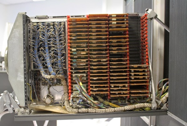
The IBM 1401 didn't use silicon chips. In fact it didn't even use silicon. Its transistors were built out of a semiconductor called germanium, which was used before silicon took over. The transistors and other components were mounted on boards the size of playing cards called SMS cards. The computer used thousands of these cards, which were installed in racks called "gates". The IBM 1401 had a couple dozen of these gates, which folded out of the computer for maintenance. Below, one of the gates is opened up showing the circuit boards and cabling.
This shows a rack (called a "gate") folded out of the IBM 1401 mainframe. The photo shows the SMS cards used to implement the circuits. This specific rack controls the tape drives.
Internally, the computer was very different from modern computers. It didn't use 8-bit bytes, but 6-bit characters based on binary coded decimal (BCD).
Since it was a business machine, the computer used decimal arithmetic instead of binary arithmetic and each character of storage held a digit, 0 through 9.
The computer came with 4000 characters of storage in magnetic core memory; a dishwasher-sized memory expansion box provided 12,000 more characters of storage.
The computer was designed to use punched cards as input, with a card reader that read the program and data. Output was printed on a fast line printer or could be punched on more cards.
The Computer History Museum in Mountain View has two working IBM 1401 mainframes. I used one of them to run the SHA-256 hash code.
For more information on the IBM 1401, see my article
Fractals on the IBM 1401.
Implementing SHA-256 on the IBM 1401
The IBM 1401 is almost the worst machine you could pick to implement the SHA-256 hash algorithm. The algorithm is designed to be implemented efficiently on machines that can do bit operations on 32-bit words. Unfortunately, the IBM 1401 doesn't have 32-bit words or even bytes. It uses 6-bit characters and doesn't provide bit operations. It doesn't even handle binary arithmetic, using decimal arithmetic instead. Thus, implementing the algorithm on the 1401 is slow and inconvenient.
I ended up using one character per bit. A 32-bit value is stored as 32 characters, either "0" or "1". My code has to perform the bit operations and additions character-by-character, basically checking each character and deciding what to do with it. As you might expect, the resulting code is very slow.
The assembly code I wrote is below.
The comments should give you a rough idea of how the code works. Near the end of the code, you can see the table of constants required by the SHA-256 algorithm, specified in hex. Since the 1401 doesn't support hex, I had to write my own routines to convert between hex and binary.
I won't try to explain IBM 1401 assembly code here, except to point out that it is very different from modern computers. It doesn't even have subroutine calls and returns. Operations happen on memory, as there aren't any general-purpose registers.
job bitcoin
* SHA-256 hash
* Ken Shirriff //righto.com
ctl 6641
org 087
X1 dcw @000@
org 092
X2 dcw @000@
org 097
X3 dcw @000@
org 333
start cs 299
r
sw 001
lca 064, input0
mcw 064, 264
w
* Initialize word marks on storage
mcw +s0, x3
wmloop sw 0&x3
ma @032@, x3
c +h7+32, x3
bu wmloop
mcw +input-127, x3 * Put input into warr[0] to warr[15]
mcw +warr, x1
mcw @128@, tobinc
b tobin
* Compute message schedule array w[0..63]
mcw @16@, i
* i is word index 16-63
* x1 is start of warr[i-16], i.e. bit 0 (bit 0 on left, bit 31 on right)
mcw +warr, x1
wloop c @64@, i
be wloopd
* Compute s0
mcw +s0, x2
za +0, 31&x2 * Zero s0
* Add w[i-15] rightrotate 7
sw 7&x2 * Wordmark at bit 7 (from left) of s0
a 56&x1, 31&x2 * Right shifted: 32+31-7 = bit 24 of w[i-15], 31 = end of s0
a 63&x1, 6&x2 * Wrapped: 32+31 = end of w[i-15], 7-1 = bit 6 of s0
cw 7&x2 * Clear wordmark
* Add w[i-15] rightrotate 18
sw 18&x2 * Wordmark at bit 18 (from left) of s0
a 45&x1, 31&x2 * Right shifted: 32+31-18 = bit 13 of w[i-15], 31 = end of s0
a 63&x1, 17&x2 * Wrapped: 32+31 = end of w[i-15], 18-1 = bit 17 of s0
cw 18&x2 * Clear wordmark
* Add w[i-15] rightshift 3
sw 3&x2 * Wordmark at bit 3 (from left) of s0
a 60&x1, 31&x2 * Right shifted: 32+31-3 = bit 28 of w[i-15], 31 = end of s0
cw 3&x2 * Clear wordmark
* Convert sum to xor
mcw x1, x1tmp
mcw +s0+31, x1 * x1 = right end of s0
mcw @032@, x2 * Process 32 bits
b xor
sw s0 * Restore wordmark cleared by xor
mcw x1tmp, x1
* Compute s1
mcw +s1, x2
za +0, 31&x2 * Zero s1
* Add w[i-2] rightrotate 17
sw 17&x2 * Wordmark at bit 17 (from left) of s1
a 462&x1, 31&x2 * Right shifted: 14*32+31-17 = bit 14 of w[i-2], 31 = end of s1
a 479&x1, 16&x2 * Wrapped: 14*32+31 = end of w[i-2], 17-1 = bit 16 of s1
cw 17&x2 * Clear wordmark
* Add w[i-2] rightrotate 19
sw 19&x2 * Wordmark at bit 19 (from left) of s1
a 460&x1, 31&x2 * Right shifted: 14*32+31-19 = bit 12 of w[i-2], 31 = end of s1
a 479&x1, 18&x2 * Wrapped: 14*32+31 = end of w[i-2], 19-1 = bit 18 of s1
cw 19&x2 * Clear wordmark
* Add w[i-2] rightshift 10
sw 10&x2 * Wordmark at bit 10 (from left) of s1
a 469&x1, 31&x2 * Right shifted: 14*32+31-10 = bit 21 of w[i-2], 31 = end of s1
cw 10&x2 * Clear wordmark
* Convert sum to xor
mcw +s1+31, x1 * x1 = right end of s1
mcw @032@, x2 * Process 32 bits
b xor
sw s1 * Restore wordmark cleared by xor
* Compute w[i] := w[i-16] + s0 + w[i-7] + s1
mcw x1tmp, x1
a s1+31, s0+31 * Add s1 to s0
a 31&x1, s0+31 * Add w[i-16] to s0
a 319&x1, s0+31 * Add 9*32+31 = w[i-7] to s0
* Convert bit sum to 32-bit sum
mcw +s0+31, x1 * x1 = right end of s0
mcw @032@, x2 * Process 32 bits
b sum
sw s0 * Restore wordmark cleared by sum
mcw x1tmp, x1
mcw s0+31, 543&x1 * Move s0 to w[i]
ma @032@, x1
a +1, i
mz @0@, i
b wloop
x1tmp dcw #5
* Initialize: Copy hex h0init-h7init into binary h0-h7
wloopd mcw +h0init-7, x3
mcw +h0, x1
mcw @064@, tobinc * 8*8 hex digits
b tobin
* Initialize a-h from h0-h7
mcw @000@, x1
ilp mcw h0+31&x1, a+31&x1
ma @032@, x1
c x1, @256@
bu ilp
mcw @000@, bitidx * bitidx = i*32 = bit index
mcw @000@, kidx * kidx = i*8 = key index
* Compute s1 from e
mainlp mcw +e, x1
mcw +s1, x2
za +0, 31&x2 * Zero s1
* Add e rightrotate 6
sw 6&x2 * Wordmark at bit 6 (from left) of s1
a 25&x1, 31&x2 * Right shifted: 31-6 = bit 25 of e, 31 = end of s1
a 31&x1, 5&x2 * Wrapped: 31 = end of e, 6-1 = bit 5 of s1
cw 6&x2 * Clear wordmark
* Add e rightrotate 11
sw 11&x2 * Wordmark at bit 11 (from left) of s1
a 20&x1, 31&x2 * Right shifted: 31-11 = bit 20 of e, 31 = end of s1
a 31&x1, 10&x2 * Wrapped: 31 = end of e, 11-1 = bit 10 of s1
cw 11&x2 * Clear wordmark
* Add e rightrotate 25
sw 25&x2 * Wordmark at bit 25 (from left) of s1
a 6&x1, 31&x2 * Right shifted: 31-25 = bit 6 of e, 31 = end of s1
a 31&x1, 24&x2 * Wrapped: 31 = end of e, 25-1 = bit 24 of s1
cw 25&x2 * Clear wordmark
* Convert sum to xor
mcw +s1+31, x1 * x1 = right end of s1
mcw @032@, x2 * Process 32 bits
b xor
sw s1 * Restore wordmark cleared by xor
* Compute ch: choose function
mcw @000@, x1 * x1 is index from 0 to 31
chl c e&x1, @0@
be chzero
mn f&x1, ch&x1 * for 1, select f bit
b chincr
chzero mn g&x1, ch&x1 * for 0, select g bit
chincr a +1, x1
mz @0@, x1
c @032@, x1
bu chl
* Compute temp1: k[i] + h + S1 + ch + w[i]
cs 299
mcw +k-7, x3 * Convert k[i] to binary in temp1
ma kidx, x3
mcw +temp1, x1
mcw @008@, tobinc * 8 hex digits
b tobin
mcw @237@, x3
mcw +temp1, x1
mcw @008@, tobinc
b tohex
a h+31, temp1+31 * +h
a s1+31, temp1+31 * +s1
a ch+31, temp1+31 * +ch
mcw bitidx, x1
a warr+31&x1, temp1+31 * + w[i]
* Convert bit sum to 32-bit sum
mcw +temp1+31, x1 * x1 = right end of temp1
b sum
* Compute s0 from a
mcw +a, x1
mcw +s0, x2
za +0, 31&x2 * Zero s0
* Add a rightrotate 2
sw 2&x2 * Wordmark at bit 2 (from left) of s0
a 29&x1, 31&x2 * Right shifted: 31-2 = bit 29 of a, 31 = end of s0
a 31&x1, 1&x2 * Wrapped: 31 = end of a, 2-1 = bit 1 of s0
cw 2&x2 * Clear wordmark
* Add a rightrotate 13
sw 13&x2 * Wordmark at bit 13 (from left) of s0
a 18&x1, 31&x2 * Right shifted: 31-13 = bit 18 of a, 31 = end of s0
a 31&x1, 12&x2 * Wrapped: 31 = end of a, 13-1 = bit 12 of s0
cw 13&x2 * Clear wordmark
* Add a rightrotate 22
sw 22&x2 * Wordmark at bit 22 (from left) of s0
a 9&x1, 31&x2 * Right shifted: 31-22 = bit 9 of a, 31 = end of s0
a 31&x1, 21&x2 * Wrapped: 31 = end of a, 22-1 = bit 21 of s0
cw 22&x2 * Clear wordmark
* Convert sum to xor
mcw +s0+31, x1 * x1 = right end of s0
mcw @032@, x2 * Process 32 bits
b xor
sw s0 * Restore wordmark cleared by xor
* Compute maj(a, b, c): majority function
za +0, maj+31
a a+31, maj+31
a b+31, maj+31
a c+31, maj+31
mz @0@, maj+31
mcw @000@, x1 * x1 is index from 0 to 31
mjl c maj&x1, @2@
bh mjzero
mn @1@, maj&x1 * majority of the 3 bits is 1
b mjincr
mjzero mn @0@, maj&x1 * majority of the 3 bits is 0
mjincr a +1, x1
mz @0@, x1
c @032@, x1
bu mjl
* Compute temp2: S0 + maj
za +0, temp2+31
a s0+31, temp2+31
a maj+31, temp2+31
* Convert bit sum to 32-bit sum
mcw +temp2+31, x1 * x1 = right end of temp1
b sum
mcw g+31, h+31 * h := g
mcw f+31, g+31 * g := f
mcw e+31, f+31 * f := e
za +0, e+31 * e := d + temp1
a d+31, e+31
a temp1+31, e+31
mcw +e+31, x1 * Convert sum to 32-bit sum
b sum
mcw c+31, d+31 * d := c
mcw b+31, c+31 * c := b
mcw a+31, b+31 * b := a
za +0, a+31 * a := temp1 + temp2
a temp1+31, a+31
a temp2+31, a+31
mcw +a+31, x1 * Convert sum to 32-bit sum
b sum
a @8@, kidx * Increment kidx by 8 chars
mz @0@, kidx
ma @032@, bitidx * Increment bitidx by 32 bits
c @!48@, bitidx * Compare to 2048
bu mainlp
* Add a-h to h0-h7
cs 299
mcw @00000@, x1tmp
add1 mcw x1tmp, x1
a a+31&x1, h0+31&x1
ma +h0+31, x1 * Convert sum to 32-bit sum
b sum
ma @032@, x1tmp
c @00256@, x1tmp
bu add1
mcw @201@, x3
mcw +h0, x1
mcw @064@, tobinc
b tohex
w
mcw 280, 180
p
p
finis h
b finis
* Converts sum of bits to xor
* X1 is right end of word
* X2 is bit count
* Note: clears word marks
xor sbr xorx&3
xorl c @000@, x2
be xorx
xorfix mz @0@, 0&x1 * Clear zone
c 0&x1, @2@
bh xorok
sw 0&x1 * Subtract 2 and loop
s +2, 0&x1
cw 0&x1
b xorfix
xorok ma @I9I@, x1 * x1 -= 1
s +1, x2 * x2 -= 1
mz @0@, x2
b xorl * loop
xorx b @000@
* Converts sum of bits to sum (i.e. propagate carries if digit > 1)
* X1 is right end of word
* Ends at word mark
sum sbr sumx&3
suml mz @0@, 0&x1 * Clear zone
c 0&x1, @2@ * If digit is <2, then ok
bh sumok
s +2, 0&x1 * Subtract 2 from digit
bwz suml, 0&x1, 1 * Skip carry if at wordmark
a @1@, 15999&x1 * Add 1 to previous position
b suml * Loop
sumok bwz sumx,0&x1,1 * Quit if at wordmark
ma @I9I@, x1 * x1 -= 1
b suml * loop
sumx b @000@ * return
* Converts binary to string of hex digits
* X1 points to start (left) of binary
* X3 points to start (left) of hex buffer
* X1, X2, X3 destroyed
* tobinc holds count (# of hex digits)
tohex sbr tohexx&3
tohexl c @000@, tobinc * check counter
be tohexx
s @1@, tobinc * decrement counter
mz @0@, tobinc
b tohex4
mcw hexchr, 0&x3
ma @004@, X1
ma @001@, X3
b tohexl * loop
tohexx b @000@
* X1 points to 4 bits
* Convert to hex char and write into hexchr
* X2 destroyed
tohex4 sbr tohx4x&3
mcw @000@, x2
c 3&X1, @1@
bu tohx1
a +1, x2
tohx1 c 2&X1, @1@
bu tohx2
a +2, x2
tohx2 c 1&x1, @1@
bu tohx4
a +4, x2
tohx4 c 0&x1, @1@
bu tohx8
a +8, x2
tohx8 mz @0@, x2
mcw hextab-15&x2, hexchr
tohx4x b @000@
* Converts string of hex digits to binary
* X3 points to start (left) of hex digits
* X1 points to start (left) of binary digits
* tobinc holds count (# of hex digits)
* X1, X3 destroyed
tobin sbr tobinx&3
tobinl c @000@, tobinc * check counter
be tobinx
s @1@, tobinc * decrement counter
mz @0@, tobinc
mcw 0&X3, hexchr
b tobin4 * convert 1 char
ma @004@, X1
ma @001@, X3
b tobinl * loop
tobinx b @000@
tobinc dcw @000@
* Convert hex digit to binary
* Digit in hexchr (destroyed)
* Bits written to x1, ..., x1+3
tobin4 sbr tobn4x&3
mcw @0000@, 3+x1 * Start with zero bits
bwz norm,hexchr,2 * Branch if no zone
mcw @1@, 0&X1
a @1@, hexchr * Convert letter to value: A (1) -> 2, F (6) -> 7
mz @0@, hexchr
b tob4
norm c @8@, hexchr
bl tob4
mcw @1@, 0&X1
s @8@, hexchr
mz @0@, hexchr
tob4 c @4@, hexchr
bl tob2
mcw @1@, 1&X1
s @4@, hexchr
mz @0@, hexchr
tob2 c @2@, hexchr
bl tob1
mcw @1@, 2&X1
s @2@, hexchr
mz @0@, hexchr
tob1 c @1@, hexchr
bl tobn4x
mcw @1@, 3&X1
tobn4x b @000@
* Message schedule array is 64 entries of 32 bits = 2048 bits.
org 3000
warr equ 3000
s0 equ warr+2047 *32 bits
s1 equ s0+32
ch equ s1+32 *32 bits
temp1 equ ch+32 *32 bits
temp2 equ temp1+32 *32 bits
maj equ temp2+32 *32 bits
a equ maj+32
b equ a+32
c equ b+32
d equ c+32
e equ d+32
f equ e+32
g equ f+32
h equ g+32
h0 equ h+32
h1 equ h0+32
h2 equ h1+32
h3 equ h2+32
h4 equ h3+32
h5 equ h4+32
h6 equ h5+32
h7 equ h6+32
org h7+32
hexchr dcw @0@
hextab dcw @0123456789abcdef@
i dcw @00@ * Loop counter for w computation
bitidx dcw #3
kidx dcw #3
* 64 round constants for SHA-256
k dcw @428a2f98@
dcw @71374491@
dcw @b5c0fbcf@
dcw @e9b5dba5@
dcw @3956c25b@
dcw @59f111f1@
dcw @923f82a4@
dcw @ab1c5ed5@
dcw @d807aa98@
dcw @12835b01@
dcw @243185be@
dcw @550c7dc3@
dcw @72be5d74@
dcw @80deb1fe@
dcw @9bdc06a7@
dcw @c19bf174@
dcw @e49b69c1@
dcw @efbe4786@
dcw @0fc19dc6@
dcw @240ca1cc@
dcw @2de92c6f@
dcw @4a7484aa@
dcw @5cb0a9dc@
dcw @76f988da@
dcw @983e5152@
dcw @a831c66d@
dcw @b00327c8@
dcw @bf597fc7@
dcw @c6e00bf3@
dcw @d5a79147@
dcw @06ca6351@
dcw @14292967@
dcw @27b70a85@
dcw @2e1b2138@
dcw @4d2c6dfc@
dcw @53380d13@
dcw @650a7354@
dcw @766a0abb@
dcw @81c2c92e@
dcw @92722c85@
dcw @a2bfe8a1@
dcw @a81a664b@
dcw @c24b8b70@
dcw @c76c51a3@
dcw @d192e819@
dcw @d6990624@
dcw @f40e3585@
dcw @106aa070@
dcw @19a4c116@
dcw @1e376c08@
dcw @2748774c@
dcw @34b0bcb5@
dcw @391c0cb3@
dcw @4ed8aa4a@
dcw @5b9cca4f@
dcw @682e6ff3@
dcw @748f82ee@
dcw @78a5636f@
dcw @84c87814@
dcw @8cc70208@
dcw @90befffa@
dcw @a4506ceb@
dcw @bef9a3f7@
dcw @c67178f2@
* 8 initial hash values for SHA-256
h0init dcw @6a09e667@
h1init dcw @bb67ae85@
h2init dcw @3c6ef372@
h3init dcw @a54ff53a@
h4init dcw @510e527f@
h5init dcw @9b05688c@
h6init dcw @1f83d9ab@
h7init dcw @5be0cd19@
input0 equ h7init+64
org h7init+65
dc @80000000000000000000000000000000@
input dc @00000000000000000000000000000100@ * 512 bits with the mostly-zero padding
end start
I punched the executable onto a deck of about 85 cards, which you can see at the beginning of the article. I also punched a card with the input to the hash algorithm. To run the program, I loaded the card deck into the card reader and hit the "Load" button. The cards flew through the reader at 800 cards per minute, so it took just a few seconds to load the program. The computer's console (below) flashed frantically for 40 seconds while the program ran. Finally, the printer printed out the resulting hash (as you can see at the top of the article) and the results were punched onto a new card. Since Bitcoin mining used double SHA-256 hashing, hashing for mining would take twice as long (80 seconds).
The console of the IBM 1401 shows a lot of activity while computing a SHA-256 hash.
Performance comparison
The IBM 1401 can compute a double SHA-256 hash in 80 seconds.
It requires about 3000 Watts of power, roughly the same as an oven or clothes dryer.
A basic IBM 1401 system sold for $125,600, which is about a million dollars in 2015 dollars.
On the other hand, today you can spend $50 and get
a USB stick miner with a custom ASIC integrated circuit.
This USB miner performs 3.6 billion hashes per second and uses about 4 watts.
The enormous difference in performance is due to several factors: the huge increase in computer speed in the last 50 years demonstrated by Moore's law, the performance lost by using a decimal business computer for a binary-based hash, and the giant speed gain from custom Bitcoin mining hardware.
To summarize, to mine a block at current difficulty, the IBM 1401 would take about 5x10^14 years (about 40,000 times the current age of the universe). The electricity would cost about 10^18 dollars. And you'd get 25 bitcoins worth about $6000. Obviously, mining Bitcoin on an IBM 1401 mainframe is not a profitable venture.
The photos below compare the computer circuits of the 1960s with the circuits of today, making it clear how much technology has advanced.
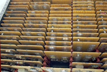
On the left, SMS cards inside the IBM 1401. Each card has a handful of components and implements a circuit such as a gate. The computer contains more than a thousand of these cards.
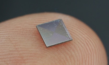
On the right, the Bitfury ASIC chip for mining Bitcoins does 2-3 Ghash/second. Image from zeptobars (CC BY 3.0 license)
Networking
You might think that Bitcoin would be impossible with 1960s technology due to the lack of networking.
Would one need to mail punch cards with the blockchain to the other computers?
While you might think of networked computers as a modern thing, IBM supported what they call teleprocessing as early as 1941. In the 1960s, the IBM 1401 could be hooked up to the
IBM 1009 Data Transmission Unit,
a modem the size of a dishwasher that could transfer up to 300 characters per second over a phone line to another computer. So it would be possible to build a Bitcoin network with 1960s-era technology. Unfortunately I didn't have teleprocessing hardware available to test this out.
IBM 1009 Data Transmission Unit. This dishwasher-sized modem was introduced in 1960 and can transmit up to 300 characters per second over phone lines. Photo from Introduction to IBM Data Processing Systems.
Conclusion
Implementing SHA-256 in assembly language for an obsolete mainframe was a challenging but interesting project.
Performance was worse than I expected (even compared to my 12 minute Mandelbrot). The decimal arithmetic of a business computer is a very poor match for a binary-optimized algorithm like SHA-256.
But even a computer that predates integrated circuits can implement the Bitcoin mining algorithm.
And, if I ever find myself back in 1960 due to some strange time warp, now I know how to set up a Bitcoin network.
The Computer History Museum in Mountain View runs demonstrations of the IBM 1401 on Wednesdays and Saturdays so if you're in the area you should definitely check it out (schedule).
Tell the guys running the demo that you heard about it from me and maybe they'll run my Pi program for you.
Thanks to the Computer History Museum and the members of the 1401 restoration team, Robert Garner, Ed Thelen, Van Snyder, and especially Stan Paddock. The 1401 team's website (ibm-1401.info) has a ton of interesting information about the 1401 and its restoration.
Disclaimers
I would like to be clear that I am not actually mining real Bitcoin on the IBM 1401—the Computer History Museum would probably disapprove of that. As I showed above, there's no way you could make money off mining on the IBM 1401. I did, however, really implement and run the SHA-256 algorithm on the IBM 1401, showing that mining is possible in theory.
And if you're wondering how I found a successful hash, I simply used a block that had already been mined:
block #286819.
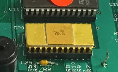
The first 8-bit microprocessor, the TMX 1795 had the same architecture as the 8008 but was built months before the 8008. Never sold commercially, this Texas Instruments processor is now almost forgotten even though it had a huge impact on the computer industry. In this article, I present the surprising history of the TMX 1795 in detail, look at other early processors, and explain how the TMX 1795 almost became the first microprocessor. (Originally I thought the TMX 1795 was the first microprocessor, but it appears that the 4004 slightly beat it.)
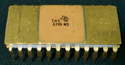
The Texas Instruments TMX 1795 microprocessor. Courtesy of Computer History Museum.
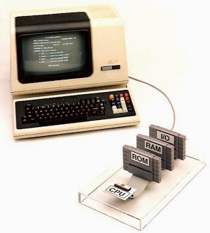
The story starts with the Datapoint 2200[1], a "programmable terminal" sized to fit on a desktop.
While originally sold as a terminal, the Datapoint 2200 was really a minicomputer that could be programmed in BASIC or PL/B.
Some people consider the Datapoint 2200 the
first personal computer as it came out years before systems such as the Apple II or even the Altair.
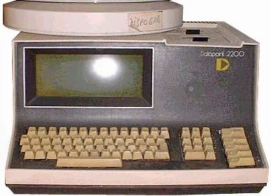
The Datapoint 2200 programmable terminal / computer. Photo by Ecksemmess CC BY-SA 3.0 via Wikimedia Commons.
The Datapoint 2200 had an 8-bit processor built out of dozens of TTL chips, which was the normal way of building computers at the time.
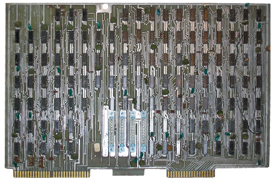
The photo below shows the processor board.
Keep in mind that there's no processor chip—the whole board is the processor, with a chip or two for each register, a few chips for the adder, a few chips to decode instructions, a few chips to increment the program counter, and so forth.
[28]
Nowadays, we think of MOS chips as high-performance and building a CPU out of TTL chips seems slow and backwards. However, in 1970, TTL logic was much faster than MOS. Even operating one bit at a time as a serial computer, the Datapoint 2200 performed considerably faster than the 8008 chip, unless it needed to wait for the slow serial memory.
The processor board from the Datapoint 2200. The 8008 was built to replace this board. Image courtesy of zuigadrummer.
While building the Datapoint 2200, its designers were looking for ways to make the processor board smaller and generate less heat. Datapoint met with Intel in December 1969, and what happened next depends on whether you listen to Intel or Datapoint.
Intel's story is that Datapoint asked if Intel could build memory chips for the processor stack that had an integrated stack pointer register.
Intel engineer Stan Mazor told Datapoint that Intel could not only do that, but could put the whole 2200 processor board on a chip.[2][3]
Datapoint's story is that Datapoint founder Gus Roche and designer Jack Frassanito suggested to Intel's co-founder Robert Noyce that Intel build a single-chip CPU with Datapoint's design.[4] but Noyce initially rejected the idea, thinking that a CPU chip wouldn't have a significant market.
In any case, Intel ended up agreeing to build a CPU chip for Datapoint using the architecture of the Datapoint 2200.[5]
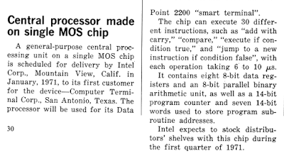
Intel developed a functional specification for the chip by June 1970 and then put the project on hold for six months. During this time, there was a mention of future 8008 chip in Electronic Design (below)—I suspect I've found the first public mention of the 8008. You might expect there was a race to build the first microprocessor, so you may be surprised that both the 4004 and 8008 projects were put on hold for months. Meanwhile, Datapoint built a switching power supply for the 2200[6], which eliminated the heating concerns, and was planning to start producing the 2200 with the processor board of TTL chips. Thus, Datapoint wasn't particularly interested in the 8008 any more.
First description of the Intel 8008 processor in print. Electronic Design, Oct 25 1970.
A Texas Instruments salesman learned that Intel was building a processor for Datapoint and asked if Texas Instruments could build them one too. Datapoint gave TI the specifications and told them to go ahead. Texas Instruments came up with a three-chip design, but came up with a single-chip CPU after Datapoint pointedly asked, "Can't you build it on one chip like Intel?" Texas Instruments started building a CPU for Datapoint around April 1970 and this chip became the TMX 1795.
There's a lot of debate on just how much information about Intel's design was given to Texas Instruments.
The main TI engineer on the project,
Gary Boone, says they received hints that Intel was doing better, but didn't improperly receive any proprietary information. According to Intel, though, Texas Instruments received Intel's detailed design documents through Datapoint. For instance, the TI processor copied an error that was in Intel's documentation leaving the TI chip with broken interrupt handling.[7]
The TI chip was first mentioned in March, 1971 in Businessweek magazine, in a short paragraph calling the chip a "milestone in LSI [Large-Scale Integration]" for jamming the CPU onto a single chip.[8]
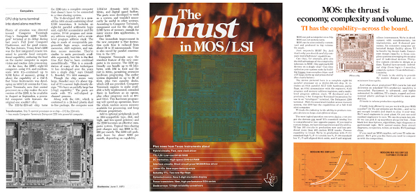
A few months later, the chip received a big media launch with an article and multi-page advertising spread in Electronics (below), complete with die photos of the TMX 1795.
Article on the TMX 1795 and two pages from the TI advertising section featuring the chip. Note the die photos of the TMX 1795. Electronics, June 7 1971.
The article, entitled "CPU chip turns terminal into stand-alone machine", described how the chip would make the Datapoint 2200 computer much more powerful. "The 212-by-224 mil chip turns the 2200 into a complete computer that doesn't have to be connected to a time-sharing system." The components of the chip are "similar to units previously available separately, but this is the first time that they've been combined monolithically", consolidated "into a single chip". The chip and 2K of memory would cost about $100. This "central processor on a chip" would make the new Datapoint 2200 "a powerful computer with features the original one couldn't offer."
That didn't happen. Datapoint tested the TMX 1795 chip and rejected it for four reasons. First, the chip and memory didn't tolerate voltage fluctuations of more than 50mV. Second, the TMX 1795 required a lot of support chips (although not as many as the 8008 would), reducing the benefit of a single-chip CPU. Third, Datapoint had solved the heat problem with a switching power supply.[6] Finally, Datapoint had just about completed the 2200 Version II, with a much faster parallel implementation of the CPU. The TMX 1795 (operating in parallel) was slightly faster than the original serial Datapoint 2200, but the 2200 Version II was much faster than the TMX 1795. (This illustrates the speed advantage of TTL chips over MOS at the time.)
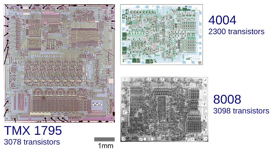
Intel engineers provided another reason for the commercial failure of the TMX 1795: the chip was too big to manufacture cost-effectively. I created the diagram below to compare the TMX 1795, 4004, and 8008 at the same scale. The TMX 1795 is larger than the 4004 and 8008 combined! One reason is that Intel had silicon-gate technology, which in effect allowed three layers of circuitry instead of two. But even taking that into account, Texas Instruments didn't seem to put much effort into the layout, which Mazor calls "pretty sloppy techniques" and "throwing some blocks together".[9] While the 4004 and especially the 8008 are densely packed, the TMX 1795 chip has copious unused and wasted space.
Comparative die sizes of the TMX 1795, 4004 and 8008 microprocessors. Note that the 4004 and 8008 are nearly the same size, while the TMX 1795 is more than twice as large. The top third of the TMX 1795 is instruction decoding and control logic, the middle is the 8-bit ALU, and the bottom is storage (stack and registers). TMX 1795 die photo courtesy of Computer History Museum.
As well as rejecting the TMX 1795, Datapoint also decided not to use the 8008 and gave up their exclusive rights to the chip. Intel, of course, commercialized the 8008, announcing it in April 1972.
Two years later, Intel released the 8080, a microprocessor based on the 8008 but with many improvements.
(Some people claim that the 8080 incorporates improvements suggested by Datapoint, but a close examination shows that later Datapoint architectures and the 8080 went in totally different directions.)
The 8080 was followed by the x86 architecture, which was designed to extend the 8080. Thus, if you're using an x86 computer now, you're using a computer based on the Datapoint 2200 architecture.[10]
Some sources dismiss the TMX 1795 as a chip that never really worked. However, the video below shows Gary Boone demonstrating the TMX 1795 in 1996. A TMX 1795 board was installed in a laptop (probably a TI LT286) for the purpose of the demo. It runs a simple text editor, a sort program, a simple budget spreadsheet, and Fibonacci numbers. The demo isn't particularly thrilling, but it shows that the TMX 1795 was a functional chip.
Considering the size of Intel and the microprocessor market, Datapoint's decision to give up exclusive rights to the 8008 seems like a huge blunder, possibly "one of the worst business decisions in history". However, it's unlikely that Datapoint would have sold 8008 chips, given that they were a computer company, not a chip company like Intel.[11] In addition, Intel had plans to produce microprocessors even without the rights to the 4004 or 8008.[12]
After rejecting the TMX 1795 (and the 8008), Datapoint continued to build processors out of TTL chips until the early 1980s. While these processors were faster and more powerful than microprocessors for a surprisingly long time, eventually Moore's law led to processors such as the 80286, which outperformed Datapoint at a lower cost. Under heavy competition from PCs, Datapoint's stock crashed in 1982, followed by a hostile takeover in 1984. The company limped along before going bankrupt in 2000. Given that Datapoint designed the architecture used in the 8008, it's ironic that Datapoint was killed by x86 microprocessors which were direct descendents of the 8008.
The TMX 1795 microprocessor installed in a circuit board. This board was used in a laptop for the 1996 demo.
Unlike Intel, who commercialized the 8008 chip, Texas Instruments abandoned the TMX 1795 after Datapoint's rejection. The chip would have disappeared without a trace, except for one thing, which had a huge impact on the computer industry.
Texas Instruments figured out early on that patent litigation and licensing fees could be very profitable.
After (co-)inventing the integrated circuit and receiving patents on it, Texas Instruments engaged in bitter patent battles, earning the nickname "the Dallas legal firm" for their "unethical and unprofessional legal tactics".[13]
Texas Instruments continued their legal practices with the TMX 1795, receiving multiple patents on it, issued between 1973 and 1985.[14][15]
Needless to say, Intel was not happy that Texas Instruments patented the TMX 1795, since building a single-chip processor for Datapoint was Intel's idea.[16]
Intel was even unhappier that that Texas Instruments had used parts of Intel's specification when designing and patenting the TMX 1795.[7][17]
Intel had wanted to patent the 4004[18], but their patent attorney told them that it wasn't worth it, and the idea of putting a computer on a chip was fairly obvious.
Likewise, Datapoint had considered patenting the single-chip microprocessor but was told by their patent attorney that there was nothing patentable in the idea.[3]
In order to extract substantial licensing fees, Texas Instruments sued multiple companies using their microprocessor and microcontroller patents (including the TMX 1795 patent) in a case that Gordon Bell called "TI v. Everybody".[13] Dell decided to fight back in a "bet the company" lawsuit.[14] The lawsuit dragged on for years and was about to go to trial when the case suddenly turned against Texas Instruments.
Lee Boysel of Four-Phase Systems had built a 24-bit MOS-based minicomputer in 1970, as will be discussed in more detail below. The computer had a 9-chip CPU, but in an amazing hack, Boysel took one of the three 8-bit arithmetic/logic chips and was able to build a working microcomputer from it. Since this chip was a year before than the TMX 1795, it torpedoed Texas Instruments' case and it never went to trial. As a result, many people consider the Four-Phase AL1 to be the first microprocessor. However, as I'll explain below, the demo wasn't quite what most people think.
The Four-Phase AL1 running as a single-chip processor in a patent litigation demo. From Boysel's EECS presentation.
Is the TMX 1795 really the first microprocessor?
There's a fair bit of argument of what is the first microprocessor. Several candidates for first microprocessor were introduced in a short period of time between 1968 and 1971. These are all interesting chips, but most of them have been forgotten. In this section, I'll discuss various candidates, but first I'll look at whether it makes sense to consider the microprocessor an invention.
Giving some hardware background will help the following discussion. The transistors you're probably most familiar with are bipolar transistors—they are fast, but bipolar integrated circuits can't contain large numbers of transistors. The TTL chips used in the Datapoint 2200 and other systems are built from bipolar transistors. A later technology produced MOS transistors, which are slower than bipolar, but can now be squeezed onto a chip by the millions or billions.
The final term is LSI or Large-Scale Integration, referring to an integrated circuit containing a large number of components: 100 gates or more. The introduction of MOS/LSI is what made it possible to build a processor with a few chips or a single chip, rather than a board full of chips.
The inevitability of microprocessors
One perspective is that the microprocessor isn't really an invention, but rather something that everyone knew would happen, and it was just a matter of waiting for the technology and market to be correct. This view is convincingly presented in Schaller's thesis,[19] which has some interesting quotes:
The idea of putting the computer on a chip
was a fairly obvious thing to do. People had
been talking about it in the literature for some
time.—Ted Hoff, 4004 designer
At the time in the early 1970s, late 1960s,
the industry was ripe for the invention of the
microprocessor.- Hal Feeney, 8008 designer
The question of ‘who invented the
microprocessor?’ is, in fact, a meaningless
one in any non-legal sense.
- Microprocessor Report
I largely agree with this perspective. It was obvious in the late 1960s that a CPU would eventually be put on a chip, and it was just a matter of time for the density of MOS chips to improve to the point that it was practical.
In addition, in the 1960s, MOS chips were slow, expensive, and unreliable[11]—a computer built out of a bunch of bipolar chips was obviously better, and this included everything from the IBM 360 mainframe to the PDP-11 minicomputer to the desktop Datapoint 2200. At first a MOS-based computer only made sense for a low-performance application (calculators, terminal), or when high density was required (aerospace, calculators).
To summarize this view, the microprocessor wasn't anything to specifically invent, but just something that happened when MOS technology improvements and a marketing need made it worthwhile to build a single chip processor.
Defining "microprocessor"
Picking the first microprocessor is largely a linguistic exercise in how you define "microprocessor". It also depends on how you define "first": this could be first design, first manufactured chips, first sales, or first patent. But I think for reasonable definitions, the TMX 1795 is first.
There's no official definition of a microprocessor. Various sources define a microprocessor as a CPU on a chip, or an arithmetic-logic unit (ALU) on a chip, or on a few chips. One interesting perspective is that "microprocessor" is basically a marketing term driven by the need of companies like Intel and Texas Instruments to give a label to their new products.[11]
In any case, I consider a microprocessor to be a CPU on a single chip, including the ALU, control, and registers. Storage and I/O is generally outside the chip. There will generally be additional support and interface chips such as buffers, latches, and clock generation.
I also consider it important that a microprocessor be programmable as a general-purpose computer.
This definition, I think, is a reasonable definition for a microprocessor.
One architecture that I don't consider a microprocessor is a microcoded system, where the control unit is separate and provides micro-instructions to control the ALU and the rest of the system.
In this system, the microcode can be provided by a ROM and a latch steps through the micro-instructions.
Since the ALU doesn't need to do instruction decoding, it can be a much simpler chip than a full-blown CPU. I don't think it's fair to call it a microprocessor.
Timeline of early microprocessors
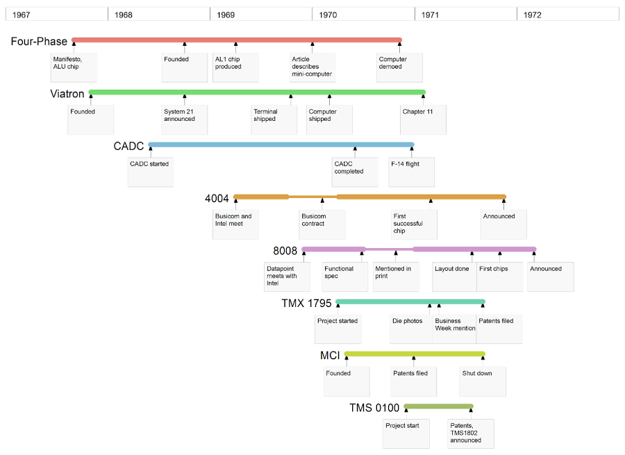
There are several processors that are frequently argued to be the first microprocessor, and they were created in a span of just a few years. I created the timeline below to show when they were developed. In the remainder of this article, I describe the different processors in detail.
Timeline of early MOS/LSI processors.
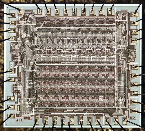
Four-Phase AL1
If one person could be considered the father of MOS/LSI processors, it would be Lee Boysel.
While working at Fairchild, he came up with the idea of a MOS-based computer and methodically designed and built the necessary cutting-edge chips (ROM in 1966, ALU in 1967, DRAM in 1968).
Along the way he published several influential articles on MOS chips, as well as a 1967 "manifesto" explaining how a computer comparable to the IBM 360 could be built from MOS.
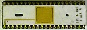
Four-Phase AL4 arithmetic-logic chip (variant of AL1)
Boysel left Fairchild and started
Four-Phase Systems in October 1968 to build his MOS-based system.
In 1970, he demoed the System/IV, a powerful 24-bit computer. The processor used 9 MOS chips: three 8-bit AL1 arithmetic / logic chips, three microcode ROMs, and three RL random logic chips.
This computer sold very well and Four-Phase became a Fortune 1000 company before being acquired by Motorola in 1981.
Die photo of Four-Phase AL1 arithmetic-logic chip. Courtesy of Computer History Museum.
As described earlier, Boysel used an AL1 chip as a processor in a courtroom demonstration system in 1995 to show prior art against TI's patents.
Given this demonstration, why don't I consider the AL1 to be the first microprocessor? It used an AL1 chip as the processor, along with ROM, RAM, and I/O and some address latches, so it seems like a single-chip CPU. But I've investigated this demonstration system closely, and while it was a brilliant hack, there's also some trickery. The ROM and its associated latch are actually set up as a microcode controller, providing 24 control lines to the rest of the system. The ROM controls memory read/write, selects an ALU operation, and provides the address of the next microcode instruction (there's no program counter). After close examination, it's clear that the AL1 chip is acting as an Arithmetic/Logic chip (thus the AL1 name), and not as a CPU.
There are a few other things that show the AL1 wasn't working as a single-chip computer.
The die photo published as part of the trial has the components of the AL1 chip labeled, including "Instruction Register 23 bits". However, that label is entirely fictional—if you study the die photo closely, there's no instruction register or 23 bits there, just vias where the ground lines pass under the clock lines. I can only conclude that this label was intended to trick people at the trial. In addition, the AL1 block diagram used at the trial has a few subtle changes from the originally-published diagram, removing the program counter and adding various interconnections. I examined the code (microcode) used for the trial, and it consists of super-bizarre microcode instructions nothing like the AL1's original instruction set.
Detail of AL1 die photo showing fictional 'Instruction Register 23 bits' label.
While the demo was brilliant and wildly successful at derailing the Texas Instruments lawsuits, I don't see it as showing the AL1 was a single-chip microprocessor. It showed that combined with a microcode controller, the AL1 could be used as a barely-functioning processor.
In addition, you could probably use a similar approach to build a processor out of an earlier ALU chip such as the 74181 or Fairchild 3800, and nobody is arguing that those are microprocessors.
Looking at the dates, it appears that Viatron (described below) shipped their MOS/LSI computer a bit before Four-Phase, so I can't call Four-Phase the first MOS/LSI computer. However, Four-Phase did produce the first computer with semiconductor memory (instead of magnetic core memory), and thus the first all-semiconductor computer.
Viatron
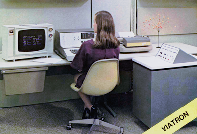
Viatron is another interesting but mostly forgotten company. It began as a hugely-publicized startup founded in November, 1967. About a year later, they announced System 21, a 16-bit minicomputer with smart terminals, tape drives, and a printer, built from custom MOS chips.
The plan was volume: by building a large number of systems, they hoped to produce the chips inexpensively and lease the systems at amazingly low prices—computer rental for $99 a month.[20] Unfortunately, Viatron ran into poor chip yields, delays, and price increases. As a result, the company went spectacularly bankrupt in March 1971.
The Viatron System 21: color display, terminal keyboard, 'robot' printer, and computer. From Viatron brochure, via bitsavers.org.
Viatron is literally the originator of the microprocessor—they were the first to use the word "microprocessor" in their October 1968 announcement of the 2101 microprocessor. However, this microprocessor wasn't a chip—it was an entire smart terminal, leasing for the incredibly low price of $20 a month.
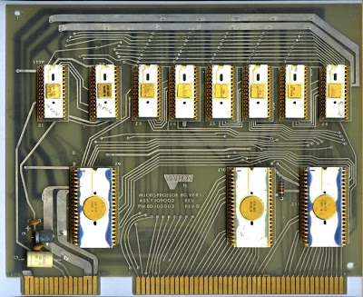
Viatron used the term microprocessor to describe the whole desktop unit complete with keyboard and tape drives. Inside the microprocessor cabinet were a bunch of boards—the processor itself consisted of 18 custom MOS chips on 3 boards, with more boards of custom MOS and CMOS chips for the keyboard interface, tape drive, memory, and video display.
The 3-board processor inside the 2101 was specialized for its terminal role. It read and wrote multiple I/O control lines, moved data between I/O devices and memory, updated the display, and provided serial input and output.[20]
The processor was very limited, not even providing arithmetic. Nonetheless, I think the Viatron 2101 "microprocessor" can be considered the first (multichip) MOS/LSI processor, shipping before the Four Phase System/IV.
CPU board #2 of three from the Viatron System 21 terminal. Top row holds two RAR register chips and six ROM chips. Bottom chips are IBR multiplexer, flag chip and ROM multiplexer, Photo courtesy of UMMR.
Viatron also built an advanced general-purpose 16-bit computer, the 62-pound 2140 minicomputer, which leased for $99 a month and came with a Fortran compiler. It had 4K 16-bit words of core memory and two 16-bit arithmetic units.
The microcoded processor had an extensive instruction set including multiply and divide operations, and supported 48-bit arithmetic.
Coming on the market slightly before the Four-Phase computer, the Viatron 2140 appears to be the first MOS/LSI general-purpose computer.
Unfortunately, sales were poor and the 2140 projected ended in 1973.
MP944 / F-14 CADC
The Central Air Data Computer was a flight control system for the F-14 fighter, using the MP944 MOS/LSI chipset developed between 1968 and 1970.
This computer processed information from sensors and generated outputs for instrumentation and to control the aircraft. The main operation it performed was computing polynomial functions on the inputs.
This chipset was designed by Ray Holt, who argues on his website
(firstmicroprocessor.com) that this 20-bit serial computer should be considered the first microprocessor.
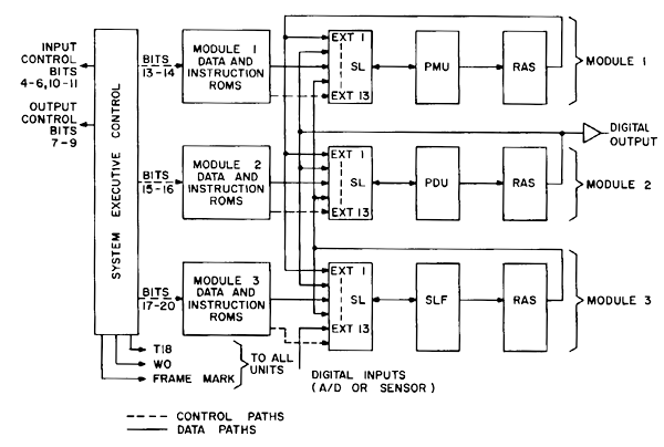
Block diagram of the F14A CADC computer.
Module 1 performs multiplication, module 2 performs division, and module 3 performs special logic functions.
From Architecture Of a Microprocessor.
The architecture of this computer is pretty unusual; it consists of three functional modules: a multiplier, a divider, and "special logic".
Each functional unit has a microcode ROM (including an address register) that provides a 20-bit microinstruction, a data steering unit (SL) that selects between 13 data inputs and performs addition, the arithmetic chip (multiply (PMU), divide (PDU) or special logic (SLF)), and a small RAM chip for storage (RAS).
Each data line transfers a 20-bit fixed-point value, shifted serially one bit at a time.
The main purpose of the SLF (special logic function) chip is to clamp a value between upper and lower bounds. It also converts Gray code to binary[21] and performs other logic functions.[22]
I don't consider this a microprocessor since the control, arithmetic, and storage are split across four separate chips in each functional unit.[23] Not only is there no CPU chip, there's not even a general-purpose ALU chip.
Computer architecture expert David Patterson says, "No way Holt's computer is a microprocessor, using the word as we mean it today."[24]
Even if you define a microprocessor as including a multi-chip processor, Viatron beat the CADC by a few months. While the CADC processor is very interesting, I don't see any way that it can be considered the first microprocessor.
Intel 4004
The well-known Intel 4004 is commonly considered the first microprocessor, but I believe the TMX 1795 beat it. I won't go into details of how Busicom contracted with Intel to have the 4004 built for a calculator, since the story is well-known.[25]
I did a lot of research into the dates of the 4004 to determine which was first: the 4004 or the TMX 1795. According to the 4004 oral history, the first successful 4004 chip was the end of February 1971 and shipped to Busicom in March.
TI wrote a draft announcement with photos of the TMX 1795 on February 24, 1971, and it was written up in Businessweek in March. The TMX 1795 was delivered to Datapoint in the summer and TI applied for a patent on August 31. The 4004 wasn't announced until November 15.
To summarize, the dates are very close but it appears that the TMX 1795 chip was built first (assuming the chip was working for the Feb 24 writeup) and announced first, while the 4004 was delivered to customers first.
On the other hand, Federico Faggin claims that the 4004 was a month or two before the TMX 1795[17].
However, the TMX 1795 was patented; I assume that someone would have mentioned in all the patent litigation if the 4004 really beat the TMX 1795 (rather than building a demo out of the Four-Phase AL1).
Based on the evidence, I conclude that the TMX 1795 was slightly before the 4004 as the first microprocessor built, while the 4004 is clearly the first microprocessor sold commercially.
Texas Instruments claims on their website: "1971: Single-chip microprocessor invented", and I agree with this claim.
Intel 8008
Many people think of the Intel 8008 as the successor to the 4004, but the two chips are almost entirely independent and were developed roughly in parallel. In fact, some of the engineers on the 4004 worried that the 8008 would come out first because the 8008 project consisted of one chip to the four in the 4004 project. The 8008 was originally called the 1201 in Intel's naming scheme because it was the first custom MOS chip Intel was developing. The 4004 would have been the 1202 except Faggin, a key engineer on the project, convinced management that 4004 was a much better name. The 1201 was renamed the 8008 before release to fit the new naming pattern.
According to my research, the 8008 may be the first microprocessor described in print. I found a reference to it (although without the 8008 name) in
a four-paragraph article in Electronic Design in Oct 25, 1970, discussing Intel's chip under development for the Datapoint 2200.
The article briefly describes the chip's instruction set, architecture, and performance.
It said the processor would be used in the 2200 "smart terminal" (which of course didn't happen), and
said the chip was scheduled for January, 1971 delivery (it slipped and was officially announced in March 1972).
Gilbert Hyatt's microcontroller patent
The story of how Gilbert Hyatt obtained a broad patent covering the microcontroller in 1990 and lost it a few years later is complex, but I will try to summarize it here.
The story starts with the founding of Micro-Computer Incorporated in 1968. Hyatt built a 16-bit serial computer out of TTL chips and sold it as a numerical control computer. He had plans to build this processor as a single chip, but before that could happen,
the company went out of business in 1971. Mr. Hyatt claims that investors Noyce and Moore (of Intel fame) cut off funding because "their motive was to sell the company and take the technology."
The Nu-troller IV CNC machine using Gilbert Hyatt's 16-bit processor built from TTL chips. Photo from Numerical Control Society Proceedings, 1971.
In 1990, seemingly out of nowhere, Gilbert Hyatt received a very general patent (4942516) covering a computer with ROM and storage on a single chip.
Hyatt had filed a patent on his computer in 1969, and due to multiple continuations, he didn't receive the patent until 1990.[15]
This patent caused considerable turmoil in the computer industry since pretty much every microcontroller was covered by this patent. Hyatt ended up receiving substantial licensing fees until Texas Instruments challenged the patent a few years later and the patent office canceled Hyatt's key patent claims.[26]
In any case, Gilbert Hyatt's microprocessor was never built (except in TTL form), there was no design for it, and the patent didn't provide any information on how to put the computer on a chip. Thus, while this computer built from TTL chips is interesting, it never became a microprocessor.
TMS 0100 calculator-on-a-chip / microcontroller
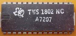
Texas Instruments created the TMS 1802NC calculator-on-a-chip in 1971; this was the first chip in the TMS 0100 series.[27] This chip included program ROM, storage, control logic and an ALU that performed arithmetic on 11-digit decimal numbers under the control of 11-bit opcodes.
The TMS 1802 calculator chip, first chip in the TMS 0100 series. Photo courtesy of datamath.org.
While the TMS 0100 series was usually called a calculator-on-a-chip, it was also intended for microcontroller tasks.
The patent describes "Programming of the calculator system for non-calculator functions", including digital volt meter, tax-fare meter, scale, cash register operations, a controller, arithmetic teaching unit, clock, and other applications.
As the first "computer-on-a-chip", the TMS 0100 gave Texas Instruments several important microcontroller patents. which they used in patent litigation (including the Dell case described earlier).[14]
(The key difference between a microcontroller and a microprocessor is the microcontroller includes the storage and program ROM, while the microprocessor has them externally.)
The TMX 1795 (first microprocessor) and TMS 0100 (first microcontroller) were both developed by Gary Boone and team (Mike Cochran, Jerry Vandierendonck, and others) at Texas Instruments almost simultaneously, which is a remarkable accomplishment.
The TMS1802NC / TMS 0100 was announced September 17, 1971.
In 1974, Texas Instruments released the successor to the TMS 0100 series, the TMS 1000 series, and marketed it as a microcontroller.
Externally, the TMS 1000 series had I/O similar to the TMS 0100 series, but internally it was entirely different. The 11-bit opcodes of the TMS 0100 were replaced by 8-bit opcodes and the 11-digit decimal storage was replaced by 4-bit binary storage.
Some sources call the TMS 1000 series the first microcontroller or first microprocessor. This is entirely wrong and based on confusion between the two series.
Confusing the TMS 0100 and TMS 1000 is like confusing the 8008 and 8080: the latter is a related, but entirely new chip.
Conclusions
Because the TMX 1795 wasn't commercially successful, the chip is almost forgotten, even though the chip has an important historical role. I've uncovered some history about this chip and take a detailed technical look at other chips that are sometimes considered the first microprocessor. The "first microprocessor" title depends on how exactly you define a microprocessor, but the TMX 1795 is first under a reasonable definition—a CPU-on-a-chip.
It's interesting, though, how multiple MOS/LSI processor chips were built in a very short span once technology permitted, and how most of them are now almost entirely forgotten.
In a future article, I'll look at the implementation and circuitry of the TMX 1795 in detail.
Thanks to Austin Roche for detailed information on Datapoint. Thanks to K. Kroslowitz of the Computer History Museum" for obtaining TMX 1795 photos for me; the chip is so obscure, there were no photos of it on the internet up until now.
Notes and references
[1]
The Datapoint Corporation was founded in 1968 as CTC (Computer Terminal Corporation), CTC later changed its name to Datapoint as the name of its product was much better known than the company name itself. For simplicity, I'll use Datapoint instead of CTC to refer to the company in this article.
[2]
The Computer History Museum's Oral History Panel on the Development and Promotion of the Intel 8008 Microprocessor discusses the history of the 8008 in great detail.
The story of the initial idea to build a single chip for Datapoint is on page 2. Texas Instruments' chip development is on page 3-4. The use of little-endian format is discussed on page 5. TI's chip is discussed on page 6. Automated design of TI's chip is on page 25.
[3]
The Computer History Museum's Oral History of Victor (Vic) Poor provides a lot of history of Datapoint. Page 34 describes Stan Mazor suggesting that Intel put Datapoint's processor on a single chip.
Page 43 describes the TI chip and its noise issues.
Page 46 explains how Datapoint's patent attorney told them there was nothing patentable about the single-chip microprocessor.
[5]
The 8008 processor was originally given the number 1201 under Intel's numbering scheme. The first digit indicated the type of circuitry: 1 for p-MOS. The second digit indicated the type of chip: 2 for random logic. The last two digits were a serial number.
For some reason, the 4004 was numbered after the 8008 and would have been the 1202. Fortunately, its developers argued that 4004 would be a better name for marketing reasons. The 1201 was later renamed the 8008 to fit this pattern. Thus, the 8008 is often though of as a successor to the 4004, even though the chips were developed in parallel and have totally different architectures.
[6]
A switching power supply is much more efficient than the less complex linear power supplies commonly used at the time, so it generates much less heat.
The Datapoint 2200 used a push-pull topology switching power supply.
Steve Jobs called the Apple II's power supply "revolutionary", saying "Every computer now uses switching power supplies, and they all rip off Rod Holt's design."
Note that the Datapoint 2200 with its swiching power supply came out 6 years before the Apple II.
I've written a lot more about the history of switching power supplies here. (By the way, don't confuse Ray Holt of the CADC with Rod Holt of Apple.)
[7]
According to Ted Hoff[18], Intel had a flaw in the original interrupt handling specification for the 8008 and TI copied that error in the TMX 1795, demonstrating that TI was using Intel specifications.
In particular, when the 8008 processor is interrupted, a RESTART instruction can be forced onto the bus, redirecting execution to the interrupt handler. The stack pointer must be updated by the RESTART instruction to save the return address, but Intel didn't include that in the initial specification. (The RESTART instruction is not part of the original Datapoint architecture.)
I've verified from the patent that the RESTART logic in the TMX 1795 doesn't update the stack pointer, so interrupt handling is broken and there's no way to return from an interrupt.
(The interrupt handling section of the TMX 1795 patent is kind of a mess. It discusses a "CONTINUE" instruction that doesn't exist.)
According to Ted Hoff, this demonstrates that Texas Instruments was using Intel's proprietary specification without entirely understanding it.
[8]
The text of the TMX 1795 announcement in Businessweek, March 27 1971, p52:
"Computer Terminal Corp., of San Antonio, Tex., has designed a
remote cathode-ray computer terminal no bigger than a typewriter that also
functions as a powerful minicomputer. In what must rank as a milestone in LSI,
Texas Instruments has managed to jam this terminal's entire central processing unit-
the equivalent of 3,100 MOS transistors-on a single custom chip roughly 2 in. square."
[10]
One enduring legacy of the Datapoint 2200 is the little-endian storage used by Intel x86 processors, which is backwards compared to most systems. Because the Datapoint 2200 had a serial processor, it accessed bits one at a time. For arithmetic, it needed to start with the lowest bit, in order to handle carries (the same as long addition starts at the right). As a consequence of this, Datapoint 2200 instructions had the low-order byte before the high-order byte. There's no need for a processor accessing bits in parallel to be little endian: processors such as the 6800 and
8051 use the more natural big-endian format. But all the microprocessors descended from the 8008 (8080, Z80, x86) kept the little-endian format used by Datapoint. (See also 8008 Oral History, page 5.)
[12]
While designing the 4004, Intel had a little-known backup plan in case the 4004 turned out to be too complex to build. This backup plan would also allow Intel to sell processors even though Busicom had exclusive rights to the 4004.
(The 4004 was built under contract to calculator manufacturer Busicom, who had exclusive rights to the 4004 (which they later gave up). Federico Faggin explains (Oral History) that while Busicom had exclusive rights to use the 4004, they didn't own the intellectual property, so Intel was free to build similar processors.)
This backup plan was the simpler 4005 chip. While the 4004 had 16 registers and an on-chip stack, the 4005 just had the program counter, a memory address register, and an accumulator, using external RAM for registers.
When the 4004 chip succeeded, Intel didn't need the 4005 and licensed it to a Canadian company,
MicroSystems International, which released the chip as the MF7114 in the second half of 1972. Sales were poor and the MF7114 was abandoned in 1973, so the chip is almost unknown today.
The history of the MF7114 is described in detail in The MIL MF7114 Microprocessor.
[14]
Texas Instruments received several broad patents on the TMX 1795.
3,757,306: "Computing Systems CPU" covers a CPU on a single chip with external memory.
4,503,511: "Computing system with multifunctional arithmetic logic unit in single integrated circuit" covers an ALU, registers, and logic on a chip.
4,225,934: "Multifunctional arithmetic and logic unit in semiconductor integrated circuit" describes an ALU on a single chip with a parallel bus.
The Texas Instruments v. Dell litigation featured multiple patents.
The TMX 1795 patent in the litigation was
4,503,511: "Computing system with multifunctional arithmetic logic unit in single integrated circuit"; the other TMX 1795 patents were not part of the litigation.
Several were TMS 0100 calculator/microcontroller patents:
4,326,265: "Variable function programmed calculator",
4,471,460: "Variable function programmed system",
4,471,461: "Variable function programmed system",
4,485,455: "Single-chip semiconductor unit and key input for variable function programmed system".
Finally there were some miscellaneous patents:
3,720,920: "Open-ended computer with selectable I/O control",
4,175,284: "Multi-mode process control computer with bit processing",
RE31,864: "Self-test feature for appliance or electronic systems operated by microprocessor".
The broader lawsuit Texas Instruments v. Daewoo, et al was against computer manufacturers Cordata (formerly Corona Data Systems), Daewoo, and Samsung. It went on from 1990 to 1993, and ended up with the companies needing to license the patents.
The Dell lawsuit, Texas Instruments v. Dell, also went from 1990 to 1993 but ended in a settlement favorable to Dell after Boysel's demonstration of the AL1 chip acting as a single-chip CPU in 1992.
[15]
It may seem strange that someone can get a patent a decade or two after their invention.
This is accomplished through a "continuation", which lets you file updated patents with additional claims. This process can be dragged out for decades, resulting in a submarine patent.
Patents used to be good for 17 years from the date it was granted, no mater how delayed.
This delay can make a patent much more valuable; there are a lot more companies to sue over a microprocessor patent in 1985 than in 1971, for instance. Plus, if you have a similar non-delayed patent too, it's like having a free extension on the patent.
US patents are now valid for 20 years from filing, eliminating submarine patents (except for those still in the system).
[16]
Ted Hoff's article Impact of LSI on future minicomputers, IEEE International Convention Digest, Mar. 1970, discusses the difficulty of building LSI parts that can be used in large (and thus cost-effective) volumes. He suggests that since a MOS chip can hold 1000 to 6000 devices, a standardized CPU could be built on a single LSI chip and sold for $10 to $20.
[17]
The 4004 Oral History has information on the 4004 timeline. Federico Faggin says that the TI chip was a month or two after the 4004 (page 32). Page 33 discusses the interrupt problem on the TMX 1795.
[18]
Interview with Marcian (Ted) Hoff (archived) provides a lot of background on development of the 4004. It describes how by October 1969 they were committed to building the 4004 as a computer on a chip. The first silicon for the 4004 was in January 1971, and by February 1971 the chip was working. In May 1971, Busicom ran into financial difficulties and negotiated a lower price for the 4004 in exchange for giving up exclusive rights to the chip.
He describes how at the Fall Joint Computer Conference, many customers would argue that the 4004 wasn't a computer but just a bit slice; after looking at the datasheet, they realized that it was a computer.
Ted Hoff also describes the origins of the 8008, saying that he and Stan Mazur proposed the single-chip processor to Datapoint, much to Vic Poor's surprise, but later Vic Poor claimed that he had planned a single-chip processor all along.
[19]
The thesis
Technological Innovation in the Semiconductor Industry by Robert R. Schaller, 2004, has several relevant chapters. Chapter 6 analyzes the history of the integrated circuit in detail. Chapter 7, The Invention of the Microprocessor, Revisited, provided a lot of background for this article. Chapter 8 is a detailed analysis of Moore's Law.
[20]
By carefully studying the Viatron terminal schematics, I uncovered details about the multi-chip processor in the Viatron terminal.
The processor handled 8-bit characters and was programmed in 12-bit microcode, 512 words stored in ROM chips. It had three data registers (IBR, TEMP, and AUX), and two microcode ROM address registers (RAR and RAAR).
Arithmetic operations appear to be entirely lacking from the processor.
The memory was built from shift register memory chips and was used for the display.
The Viatron price list is in the Viatron System 21 Brochure.
[21]
The Gray code is a way of encoding values in binary so only one bit changes at a time. This is useful for mechanical encoding because it avoids errors during transitions. For instance, if you use binary to encode the position of an aircraft control, as it moves from 3 to 4 the binary values are 011 and 100. If the first bit changes before the rest, you get 111 (i.e. 7) and your plane may crash. With Gray code, 3 and 4 are encoded as 010 and 110. Since only one bit changes, it doesn't matter if the bits don't change simultaneously—you either have 3 or 4 and no bad values in between.
[22]
Ray Holt's firstmicroprocessor.com calls the SLF (special logic function) chip the CPU.
In the original paper, this chip was not called the CPU and was only described briefly. In the paper, each of the three multi-chip functional units is called a CPU.
It's clear that the SLF chip was recently renamed the CPU just to support the claim that the CADC was the first microprocessor.
[23]
The MP944 chips had considerably fewer transistors than the 4004: 1063 in the PMU, 1241 in the PDU, 743 in the SLF, and 771 in the SLU, compared to 2300 in the 4004.
[24]
David Patterson's analysis of the CADC computer can be found on the
firstmicroprocessor.com website.
[27]
Note that the TMS 0100 is actually a series of chips (TMS 01XX) and likewise the TMS 1000 is also a series.
Confusingly, the first chip in the TMS 0100 series was the TMS 1802NC calculator chip, which was renamed the TMS 0102; despite its name, it was not in the TMS 1000 series.
[28]
The Datapoint 2200 was a serial processor—while it was an 8-bit processor, it operated on one bit at a time, had a one-bit ALU, and a one-bit internal bus. While this seems bizarre from our perspective, implementing a processor serially was a fairly common way to reduce the cost of a processor; the PDP-8/S was another serial minicomputer.
(This should not be confused with the Motorola MC14500B, which genuinely is a one-bit processor designed for simple control applications.)