Standard cells: Looking at individual gates in the Pentium processor

Intel released the powerful Pentium processor in 1993, a chip to "separate the really power-hungry folks from ordinary mortals." The original Pentium was followed by the Pentium Pro, the Pentium II, and others, spawning a long-running brand of high-performance processors, Intel's flagship line until the Core processors took over in 2006. The Pentium eventually became virtually synonymous with "PC" and even made it into pop culture.

Even though the Pentium is a complex chip with 3.3 million transistors, its transistors are visible under a microscope, unlike modern chips. By examining the chip, we can see the interesting circuits used for gates, flip-flops, and other circuits, including the use of an unusual technology called BiCMOS. In this article, I take a close look at the original Pentium chip1, showing how much of its circuitry was built out of structured rows of tiny transistors, a technique known as standard-cell design.

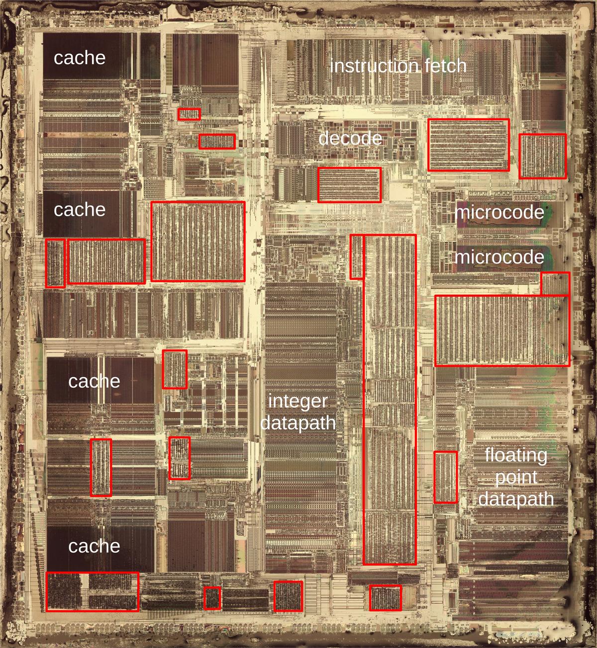
The die photo below shows the Pentium's fingernail-sized silicon die under a microscope. I removed the chip's four metal layers to show the underlying silicon, revealing the individual transistors, which are obscured in most die photos by the layers of metal. Standard-cell circuitry, indicated by red boxes, is recognizable because the circuitry is arranged in uniform columns of cells, giving it a characteristic striped appearance. In contrast, the chip's manually-optimized functional blocks are denser and more structured, giving them a darker appearance. Examples are the caches on the left, the datapaths in the middle, and the microcode ROMs on the right.

Die photo of the Intel Pentium processor with standard cells highlighted in red. The edges of the chip suffered some damage when I removed the metal layers. Click this image (or any other) for a larger version.

Die photo of the Intel Pentium processor with standard cells highlighted in red. The edges of the chip suffered some damage when I removed the metal layers. Click this image (or any other) for a larger version.

Standard-cell design

Early processors in the 1970s were usually designed by manually laying out every transistor individually, fitting transistors together like puzzle pieces to optimize their layout. While this was tedious, it resulted in a highly dense layout. Federico Faggin, designer of the popular Z80 processor, was almost done when he ran into a problem. The last few transistors wouldn't fit, so he had to erase three weeks of work and start over. The closeup of the resulting Z80 layout below shows that each transistor has a different, complex shape, optimized to pack the transistors as tightly as possible.2

A closeup of transistors in the Zilog Z80 processor (1976). This chip is NMOS, not CMOS, which provides more layout flexibility. The metal and polysilicon layers have been removed to expose the underlying silicon. The lighter stripes over active silicon indicate where the polysilicon gates were. I think this photo is from the Visual 6502 project but I'm not sure.

A closeup of transistors in the Zilog Z80 processor (1976). This chip is NMOS, not CMOS, which provides more layout flexibility. The metal and polysilicon layers have been removed to expose the underlying silicon. The lighter stripes over active silicon indicate where the polysilicon gates were. I think this photo is from the Visual 6502 project but I'm not sure.

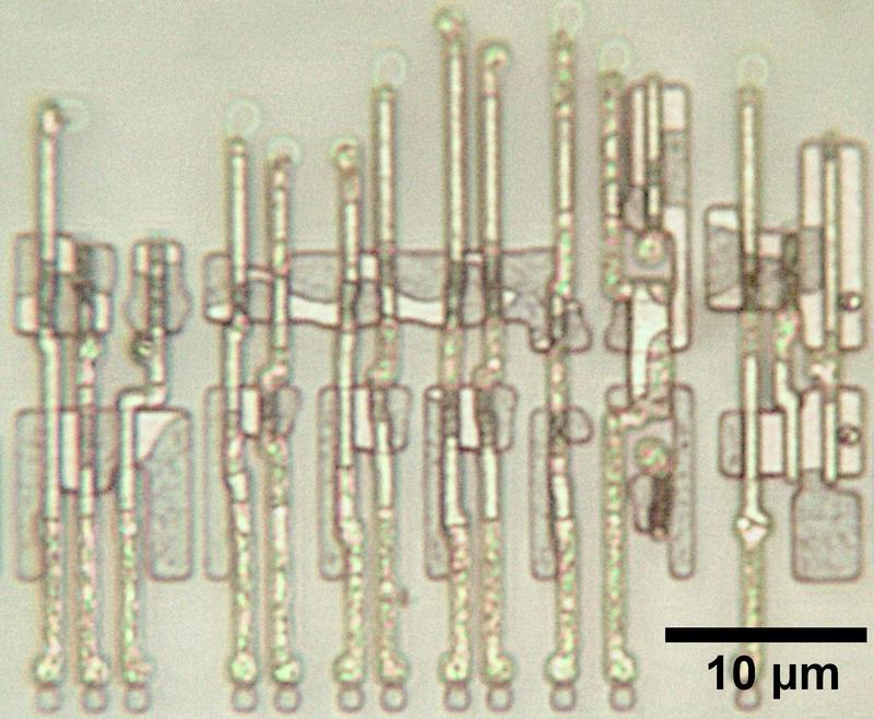
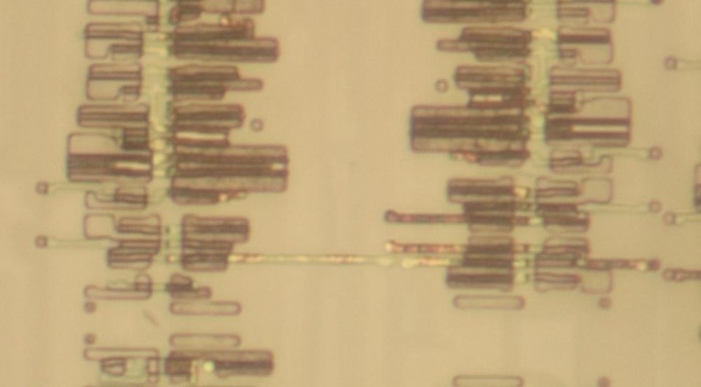
Because manual layout is slow, difficult, and error-prone, people developed automated approaches such as standard-cell.3 The idea behind standard-cell is to create a standard library of blocks (cells) to implement each type of gate, flip-flop, and other low-level component. To use a particular circuit, instead of arranging each transistor, you use the standard design from the library. Each cell has a fixed height but the width varies as needed, so the standard cells can be arranged in rows. The Pentium die photo below shows seven cells in a row. (The rectangular blobs are doped silicon while the long, thin vertical lines are polysilicon.) Compare the orderly arrangement of these transistors with the Z80 transistors above.

Some standard cell circuitry in the Pentium.
I removed the metal to show the underlying silicon and polysilicon.

Some standard cell circuitry in the Pentium. I removed the metal to show the underlying silicon and polysilicon.

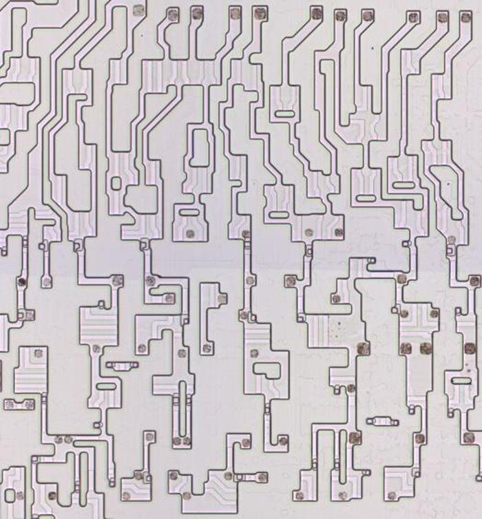
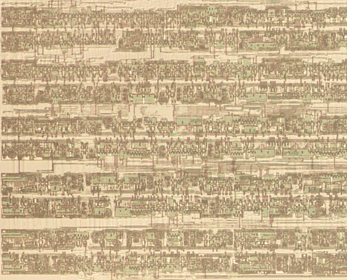
The photo below zooms out to show five rows of standard cells (the dark bands) and the wiring in between. Because CMOS circuitry uses two types of transistors (NMOS and PMOS), each standard-cell row appears as two closely-spaced bands: one of NMOS transistors and one of PMOS transistors. The space between rows is used as a "wiring channel" that holds the wiring between the cells. Power and ground for the circuitry run along the top and bottom of each row.

Some standard cells in the Pentium processor.

Some standard cells in the Pentium processor.

The fixed structure of standard cell design makes it suitable for automation, with the layout generated by "automatic place and route" software. The first step, placement, consists of determining an arrangement of cells that minimizes the distance between connected cells. Running long wires between cells wastes space on the die, since you end up with a lot of unnecessary metal wiring. But more importantly, long paths have higher capacitance, slowing down the signals. Once the cells are placed in their positions, the "routing" step generates the wiring to connect the calls. Placement and routing are both difficult optimization problems that are NP-complete.

Intel started using automated place and route techniques for the 386 processor, since it was much faster than manual layout and dramatically reduced the number of errors. Placement was done with a program called Timberwolf, developed by a Berkeley grad student. As one member of the 386 team said, "If management had known that we were using a tool by some grad student as a key part of the methodology, they would never have let us use it." Intel developed custom software for routing, using an iterative heuristic approach. Standard-cell design is still used in current processors, but the software is much more advanced.

A brief overview of CMOS

Before looking at the standard cell circuits in detail, I'll give a quick overview of how CMOS circuits are implemented. Modern processors are built from CMOS circuitry, which uses two types of transistors: NMOS and PMOS. The diagram below shows how an NMOS transistor is constructed. The transistor can be considered a switch between the source and drain, controlled by the gate. The source and drain regions (green) consist of silicon doped with impurities to change its semiconductor properties, forming N+ silicon. The gate consists of a layer of polysilicon (red), separated from the silicon by a very thin insulating oxide layer. Whenever polysilicon crosses active silicon, a transistor is formed. Diagram showing the structure of an NMOS transistor.
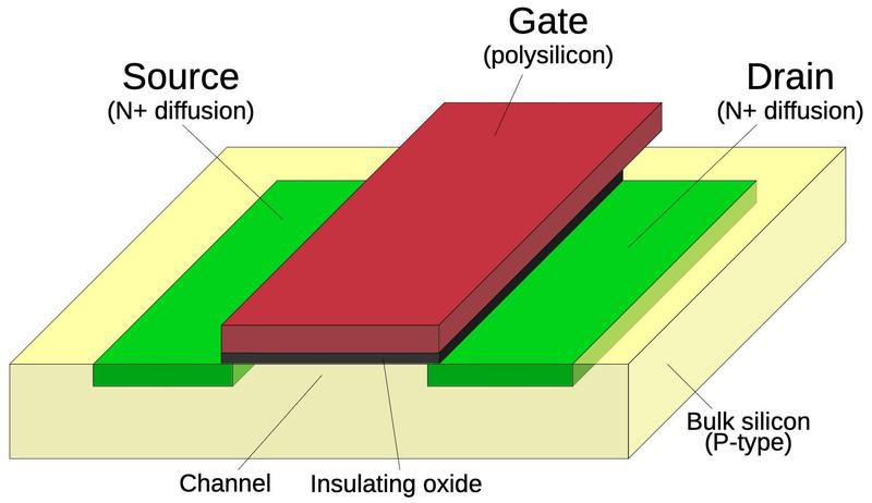
Diagram showing the structure of an NMOS transistor.

The NMOS and PMOS transistors are opposite in their construction and operation. A PMOS transistor swaps the N-type and P-type silicon, so it consists of P+ regions in a substrate of N silicon. In operation, an NMOS transistor turns on when the gate is high, while a PMOS transistor turns on when the gate is low.4 An NMOS transistor is best at pulling its output low, while a PMOS transistor is best at pulling its output high. In a CMOS circuit, the transistors work as a team, pulling the output high or low as needed; the "C" in CMOS indicates this "Complementary" approach. NMOS and PMOS transistors are not entirely symmetrical, however, due to the underlying semiconductor physics. Instead, PMOS transistors need to be larger than NMOS transistors, which helps to distinguish PMOS transistors from NMOS transistors on the die.

The layers of circuitry in the Pentium

The construction of the Pentium is more complicated than the diagram above, with four layers of metal wiring that connect the transistors.5 Starting at the surface of the silicon die, the Pentium's transistors are similar to the diagram, with regions of silicon doped to change their semiconductor properties. Polysilicon wiring is created on top of the silicon. The most important role of the polysilicon is that when it crosses doped silicon, a transistor is formed, with the polysilicon as the gate. However, polysilicon is also used as wiring over short distances.

Above the silicon, four layers of metal connect the components: multiple metal layers allow signals to crisscross the chip without running into each other. The metal layers are numbered M1 through M4, with M1 on the bottom. A few rules control the wiring: a metal layer can connect with the layer above or below through a tungsten plug called a "via". Only the bottom metal, M1, can connect to the silicon or polysilicon, through a "contact". The layers usually alternate between horizontal wiring and vertical wiring (at least locally). Thus, a signal from a transistor may travel through M1, bounce up to M2 and M3 to cross other signals, and then go back down to M1 to connect to another transistor. As you can see, automated place and route software has a complicated task, producing millions of complicated wiring paths as densely as possible.

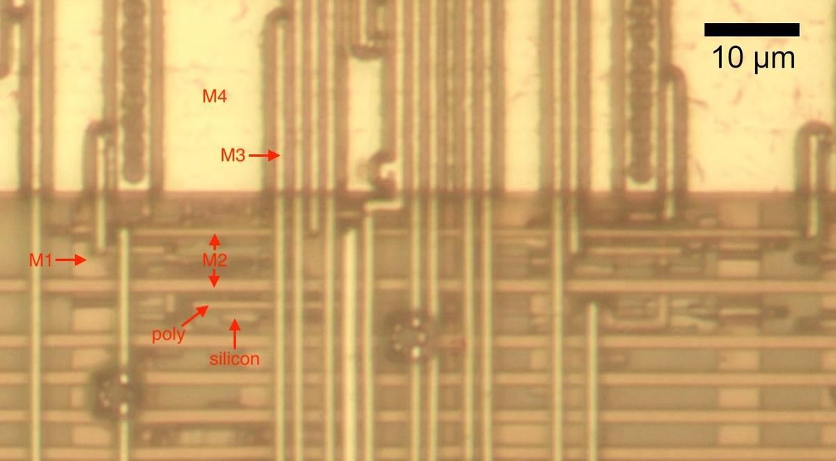
The diagram below shows how the layers appear on the chip. (This photo shows one of the rare spots on the chip where all the layers are visible.) The M4 metal layer on top of the chip is the thickest, so it is mostly used for power, ground, and clock signals rather than data. An M4 ground wire covers the top of this photo. The next layer down is M3. In this part of the chip, M3 lines run vertically. (Due to optical effects, the vertical M3 lines may look like they are on top of M4, but they are below.) The horizontal M2 metal lines are lower and appear brown rather than golden, due to the oxide layers that cover them. The bottom metal layer is M1. The vertical M1 lines are thick in this part of the chip because they provide power to the circuitry.

The Pentium is constructed with four layers of metal. Because the chip has a three-dimensional structure, I used focus stacking to get a clearer image.

The Pentium is constructed with four layers of metal. Because the chip has a three-dimensional structure, I used focus stacking to get a clearer image.

The silicon and polysilicon are mostly obscured in the above photo. By removing all the metal layers, I obtained the image below. This image shows the same region as the image above, but it is hard to see the correlation because the metal layers almost completely obscure the silicon. The orderly columns of transistors reveal the standard-cell design. The irregular dark regions are doped silicon, which forms the chip's transistors. The dark or shiny horizontal bands are polysilicon. I will explain below how these regions form gates and other circuits.

A closeup of the silicon and polysilicon.

A closeup of the silicon and polysilicon.

Inverter

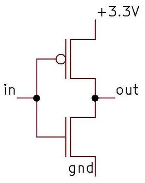
The fundamental CMOS gate is an inverter, shown in the schematic below. The inverter is built from one PMOS transistor (top) and one NMOS transistor (bottom). If the gate input is a "1", the bottom transistor turns on, pulling the output to ground (0). A "0" input turns on the top transistor, pulling the output high (1). Thus, this two-transistor circuit implements an inverter.10

Schematic diagram of a CMOS inverter.

Schematic diagram of a CMOS inverter.

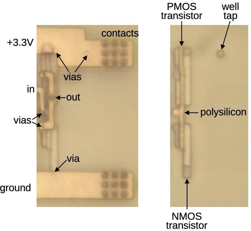
The diagram below shows two views of how a standard-cell inverter appears on the Pentium die, with and without metal. The inverter consists of two transistors, just like the schematic above. The input is connected to the two polysilicon gates of the transistors. The metal output wire is connected to the two transistors (the left sides, specifically).

A standard-cell CMOS inverter in the Pentium.

A standard-cell CMOS inverter in the Pentium.

In more detail, the image on the left includes the bottom (M1) metal layer, but I removed the other metal layers. Two thick metal lines at the top and bottom provide power and ground to the standard cells. The multiple dark circles are contacts between the M1 metal layer and the metal layer on top (M2), providing a path for power and ground that eventually reaches the top (M4) metal layer and then the chip's pins. (The power and ground wires are thick to provide sufficient current to the circuitry while minimizing voltage drops and noise.) The small, lighter circles are vias that connect the M1 metal layer to the underlying silicon or polysilicon. The input to the gate is provided from the M2 metal, which connects to the M1 layer at the indicated contact. The smaller black dots at the top and bottom of this metal strip are vias, connections to the underlying silicon.

For the image on the right, I removed all four metal layers, revealing the polysilicon and doped silicon. Recall that a transistor is constructed from regions of doped silicon with a stripe of polysilicon between the regions, forming the transistor's gate. The diagram shows the two transistors that form the inverter. When combined with the metal wiring, they form the inverter schematic shown earlier. The final feature is the "well tap". The PMOS transistors are constructed in a "well" of N-doped silicon. The well must be kept at a positive voltage, so periodic "taps" connect the well to the +3.3V supply. As mentioned earlier, the PMOS transistor is larger than the NMOS transistor, which allowed me to figure out the transistor types in the photo.

By the way, the chip is built with a 600 nm process, so the width of the polysilicon lines is approximately 600 nm. For comparison, the wavelength of visible light is 400 to 700 nm, with 600 nm corresponding to orange light. This explains why the microscope photos are somewhat fuzzy; the features are the size of the wavelength of light.6

NAND gate

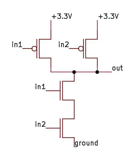
Another common gate in the Pentium is the NAND gate. The schematic below shows a NAND gate with two PMOS transistors above and two NMOS transistors below. If both inputs are high, the two NMOS transistors turn on, pulling the output low. If either input is low, a PMOS transistor turns on, pulling the output high. (Recall that NMOS and PMOS are opposites: a high voltage turns an NMOS transistor on while a low voltage turns a PMOS transistor on.) Thus, the CMOS circuit below produces the desired output for the NAND function.

Schematic of a CMOS NAND gate.

Schematic of a CMOS NAND gate.

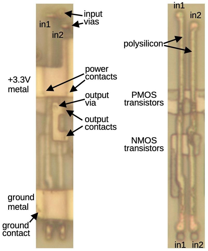
The implementation of the gate as a standard cell, below, follows the schematic. The left photo shows the circuit with one layer of metal (M1). A thick metal line provides 3.3 volts to the gate; it has two contacts that provide power to the two PMOS transistors. The metal line for ground is similar, except only one NMOS transistor is grounded. The thinner metal in the middle has two contacts to get the transistor outputs and a via to connect the output to the M2 metal layer on top. Finally, two tiny bits of M1 metal connect the inputs from the M2 layer to the underlying polysilicon.

Implementation of a CMOS NAND gate as a standard cell.

Implementation of a CMOS NAND gate as a standard cell.

The right photo shows the circuit with all metal removed, showing the polysilicon and silicon. Since a transistor is formed where a polysilicon line crosses doped silicon, the two polysilicon lines create four transistors. Polysilicon functions both as local wiring and as the transistor gates. In particular, the inputs can be connected at the top or bottom of the circuit (or both), depending on what works best for wiring the circuitry. Note that the transistors are squashed together so the silicon in the middle is part of two transistors. An important asymmetry is that the output is taken from the middle of the PMOS transistors, wiring them in parallel, while the output is taken from the right side of the NMOS transistors, wiring them in series.

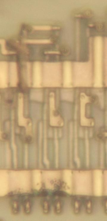
Zooming out a bit, the photo below shows three NAND gates. Although the underlying standard cell is the same for each one, there are differences between the gates. At the top, horizontal wiring links the inputs to M2 through vias. The length of each polysilicon line depends on the position of the metal. Moreover, in the middle of each gate, the metal connection to the output is positioned differently. Finally, note that the power wiring shifts upward in the upper right corner; this is to make room for a larger cell to the right. The point is that the standard cells aren't simply copies of each other, but are adjusted in each case to put the inputs, outputs, and power in the right location. Also note that these standard cells are not isolated, but are squeezed together so the PMOS transistors are touching. This optimization slightly increases the density.

Three NAND gates in the Pentium.

Three NAND gates in the Pentium.

OR-NAND gate

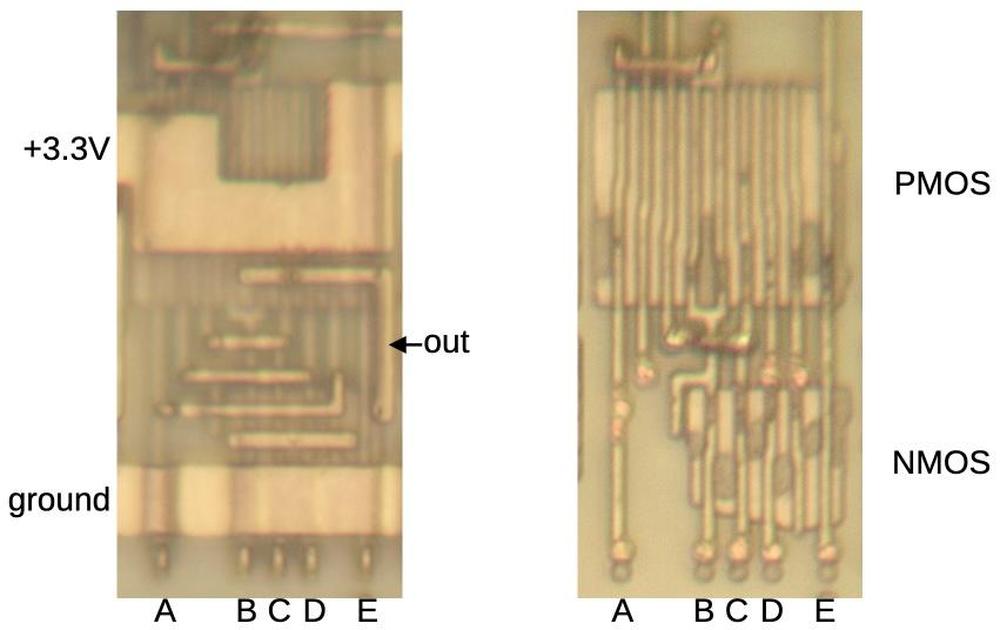
The standard cell library includes some complex gates. For instance, the gate below is a 5-input OR-NAND gate, computing ~((A+B+C+D)⋅E). In the NMOS circuit, transistors A through D are paralleled while E is in series. The PMOS circuit is the opposite, with A through D in series and E in parallel. To provide sufficient current, the PMOS circuit has two sets of transistors for A through D, so the PMOS block is much larger than the NMOS block.

The OR-NAND gate as it appears on the die. The left image shows the M1 metal layer while the right image shows the silicon
and polysilicon.

The OR-NAND gate as it appears on the die. The left image shows the M1 metal layer while the right image shows the silicon and polysilicon.

Latch

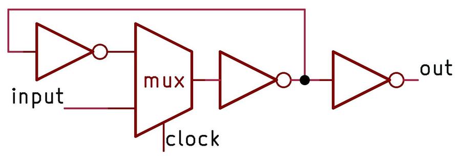
One of the key building blocks of the Pentium's circuitry is the latch. The idea of the latch is to hold one bit, controlled by the clock signal. A latch is "transparent": the latch's input immediately appears on the output while the clock is high. But when the clock is low, the latch holds its previous value. The latch is implemented with a feedback loop that passes the latch's output back into the latch. The heart of this latch circuit is the multiplexer (mux), which selects either the previous output (when the clock is low) or the new input (when the clock is high). The inverters amplify the feedback signal so it doesn't decay in the loop. An inverter also amplifies the output so it can drive other circuitry.

The circuit for a latch.

The circuit for a latch.

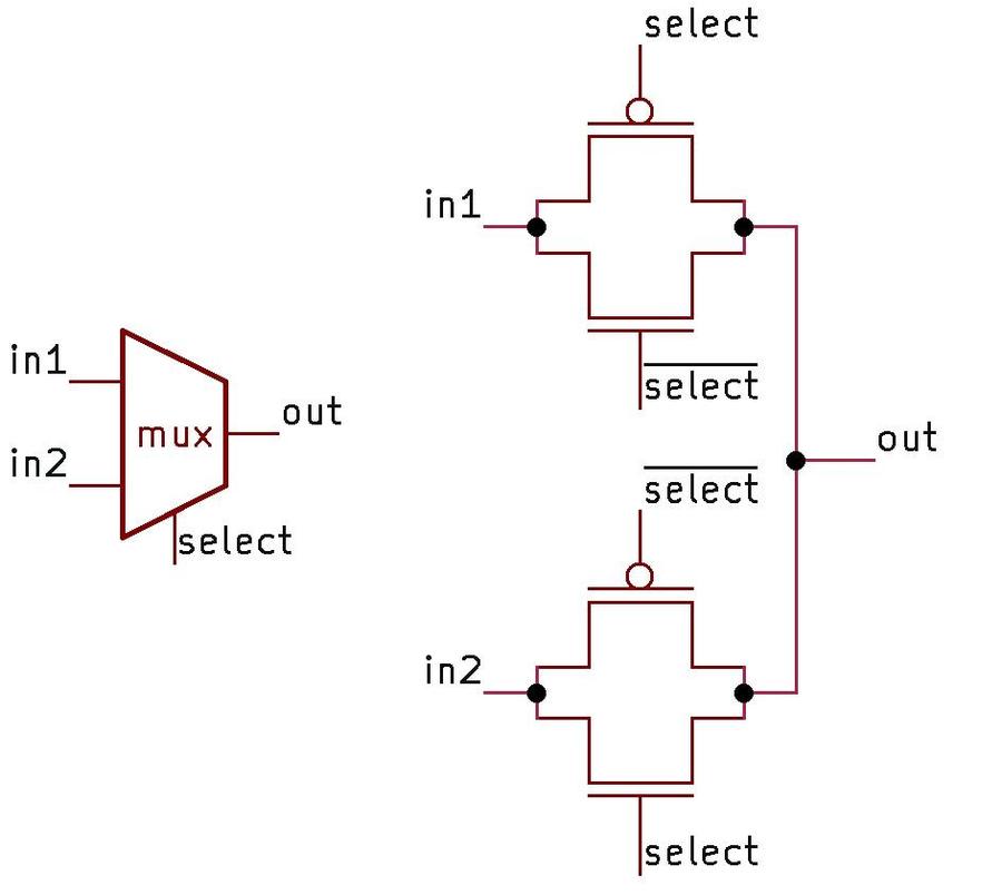
The circuit for a multiplexer is interesting since it uses "pass transistors". That is, the transistors simply pass their input through to the output, rather than pulling a signal to power or ground as in a typical logic gate. The schematic shows how this works. First, suppose that the select line is low. This will turn on the two transistors connected to the first input, allowing its level to flow to the output. Meanwhile, both transistors connected to the second input will be turned off, blocking that signal. But if the select line is high, everything switches. Now, the two transistors connected to the second input turn on, passing its level to the output. Thus, the multiplexer selects the first input if the control signal is low, and the second input if the control signal is high.

A multiplexer and its implementation in CMOS.

A multiplexer and its implementation in CMOS.

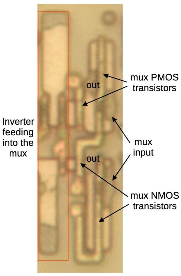
The diagram below shows a multiplexer, part of a latch. On the left, an inverter feeds into one input of the multiplexer.7 On the right is the other input to the multiplexer. The output is taken from the middle, between the pairs of the transistors.

A multiplexer as it appears on the Pentium die.

A multiplexer as it appears on the Pentium die.

Note that the multiplexer's circuit is opposite, in a way, to a logic gate. In a logic gate, you want either the NMOS transistor on or the PMOS transistor on, so the output is pulled low or high respectively. This is accomplished by giving the signals on the transistor gates the same polarity, so the same polysilicon line runs through both transistors. In a multiplexer, however, you want the corresponding PMOS and NMOS transistors to turn on at the same time, so they can pass the signal. This requires the signals on the transistor gates to have opposite polarity. One polysilicon line runs through the right PMOS transistor and the left NMOS transistor. The other polysilicon line runs through the left PMOS transistor and the right NMOS transistor, connected by metal wiring (not shown). The multiplexer includes an inverter to provide the necessary signal, but I cropped it out of the diagram below.

The flip-flop

The Pentium makes extensive use of flip-flops. A flip-flop is similar to a latch, except its clock input is edge-sensitive instead of level-sensitive. That is, the flip-flop "remembers" its input at the moment the clock goes from low to high, and provides that value as its output. This difference may seem unimportant, but it turns out to make the flip-flop more useful in counters, state machines, and other clocked circuits.

In the Pentium, a flip-flop is constructed from two latches: a primary latch and a secondary latch. The primary latch passes its value through while the clock is low and holds its value when the clock is high. The output of the primary latch is fed into the secondary latch, which has the opposite clock behavior. The result is that when the clock switches from low to high, the primary latch stops updating its output at the same time that the secondary starts passing this value through, providing the desired flip-flop behavior.

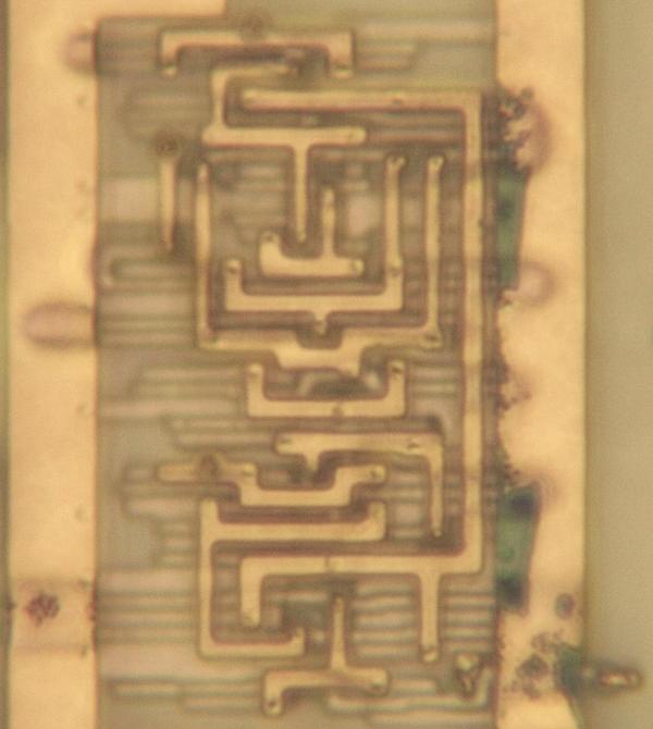
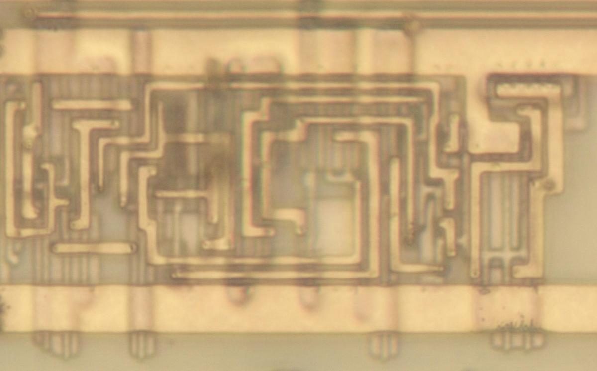
A standard-cell flip-flop.

A standard-cell flip-flop.

The photo above shows a standard-cell flop-flop, with an intricate pattern of metal wiring connecting the various sub-components. There are a few variants; with minor logic changes, the flip-flop can have "set" or "reset" inputs, bypassing the clock to force the output to the desired state. (Set and reset functions are useful for initializing flip-flops to a desired value, for example when the processor starts up.)

The BiCMOS buffer

Although I've been discussing CMOS circuits so far, the Pentium was built with BiCMOS, a process that allows circuits to use bipolar transistors in addition to CMOS. By adding a few extra processing steps to the regular CMOS manufacturing process, bipolar (NPN and PNP) transistors can be created. The Pentium made extensive use of BiCMOS circuits since they reduced signal delays by up to 35%. Intel also used BiCMOS for the Pentium Pro, Pentium II, Pentium III, and Xeon processors (but not the Pentium MMX). However, as chip voltages dropped, the benefit from bipolar transistors dropped too and BiCMOS was eventually abandoned.

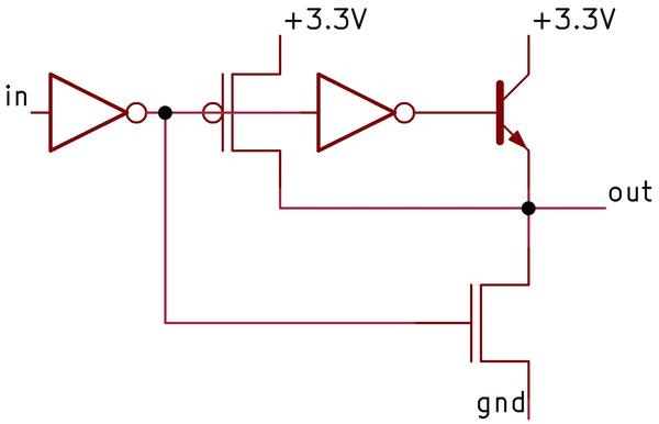
The schematic below shows a standard-cell BiCMOS buffer in the Pentium chip.8 This circuit is more complex than a CMOS buffer: it uses two inverters, an NPN pull-up transistor, an NMOS pull-down transistor, and a PMOS pull-up transistor.9

Reverse-engineered schematic of the BiCMOS buffer.

Reverse-engineered schematic of the BiCMOS buffer.

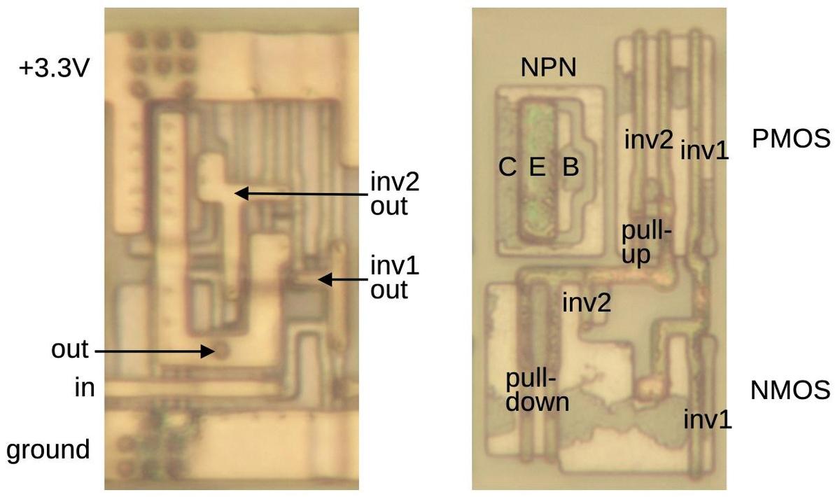
In the die images below, note the circular structure of the NPN transistor, very different from the linear structure of the NMOS and PMOS transistors and considerably larger. A sign of the buffer's high-current drive capacity is the output's thick metal wiring, much thicker than the typical signal wiring.

A BiCMOS buffer in the Pentium.

A BiCMOS buffer in the Pentium.

Conclusions

Standard-cell layout is extensively used in modern chips. Modern processors, with their nanometer-scale transistors, are much too small to study under a microscope. The Pentium, on the other hand, has features large enough that its circuits can be observed and reverse engineered. Of course, with 3.3 million transistors, the Pentium is too much for me to reverse engineer in depth, but I still find it interesting to study small-scale circuits and see how they were implemented. This post presented a small sample of the standard cells in the Pentium. The full standard-cell library is much larger, with dozens, if not hundreds, of different cells: many types of logic gates in a variety of sizes and drive strengths. But the fundamental design and layout principles are the same as the cells described here.

One unusual feature of the Pentium is its use of BiCMOS circuitry, which had a peak of popularity in the 1990s, right around the era of the Pentium. Although changing tradeoffs made BiCMOS impractical for digital circuitry, BiCMOS still has an important role in analog ICs, especially high-frequency applications. The Pentium in a sense is a time capsule with its use of BiCMOS.

I hope that you have enjoyed this look at some of the Pentium's circuits. I find it reassuring to see that even complex processors are made up of simple transistor circuits and you can observe and understand these circuits if you look closely.

For more on standard-cell circuits, I wrote about standard cells in an IBM chip and standard cells in the 386 (the 386 article has a lot of overlap with this one). Follow me on Twitter @kenshirriff or RSS for updates. I'm also on Mastodon occasionally as @[email protected].

Notes and references

  1. In this blog post, I'm focusing on the "P54C" version of the original Pentium processor. Intel produced many different versions of the Pentium, and it can be hard to keep them straight. Part of the problem is that "Pentium" is a brand name, with multiple microarchitectures, lines, and products. At the high level, the Pentium (1993) was followed by the Pentium Pro (1995) Pentium II (1997), Pentium III (1999), Pentium 4 (2000), and so on. The original Pentium used the P5 microarchitecture, a superscalar microarchitecture that was advanced but still executed instruction in order like traditional microprocessors. The Pentium Pro was a major jump, implementing a microarchitecture called P6 that broke instructions into micro-operations and executed them out of order using dataflow techniques. The next microarchitecture version was NetBurst, first used with the Pentium 4. NetBurst provided a deep pipeline and introduced hyper-threading, but it was disappointingly slow and was replaced by the Core microarchitecture. The Core microarchitecture is based on the P6 and is Intel's current microarchitecture.

    I'll focus now on the original Pentium, which went through several substantial revisions. The first Pentium product was the 80501 (codenamed P5), running at 60 or 66 MHz and using 5 volts. These chips were built with an 800 nm process and contained 3.1 million transistors.

    The power consumption of these chips was disappointing, so Intel improved the chip, producing the 80502. These chips, codenamed P54C, used 3.3 volts and ran at 75-120 MHz. The chip's architecture remained essentially the same but support was added for multiprocessing, boosting the transistor count to 3.3 million. The P54C had a much more advanced clock circuit, allowing the external bus speed to stay low (50-66 MHz) while the internal clock speed—and thus performance—climbed to 100 MHz. The chips were built with a smaller 600 nm process with four layers of metal, compared to the previous three. Visually, the die of the P54C is almost the same as the P5, with the additional multiprocessing logic at the bottom and the clock circuitry at the top. For this article, I examined the P54C, but the standard cells should be similar in other versions.

    Next, Intel moved to the 350 nm process, producing a smaller, faster Pentium chip, codenamed the P54CS; the die looks almost identical to the P54C (but smaller), with subtle changes to the bond pads. Another variant was designed for mobile use: the Pentium processor with "Voltage Reduction Technology" reduced power consumption by using a 2.9- or 3.1-volt supply for the core and a 3.3-volt supply to drive the I/O pins. These were built first with the 600 nm process (75-100 MHz) and then the 350 nm process (100-150 MHz).

    The biggest change to the original Pentium was the Pentium MMX, with part number 80503 and codename P55C. This chip extended the x86 instruction set with 57 new instructions for vector processing. It was built on a 350 nm process before moving to 280 nm, and had 4.5 million transistors. More obscure variants of the original Pentium include the P54CQS, P54CS, P54LM, P24T, and Tillamook, but I won't get into them. 

  2. Circuits that had a high degree of regularity, such as the arithmetic/logic unit (ALU) or register storage were typically constructed by manually laying out a block to implement the circuitry for one bit and then repeating the block as needed. Because a circuit was repeated 32 times for the 32-bit processor, the additional effort was worthwhile. 

  3. An alternative layout technique is the gate array, which doesn't provide as much flexibility as a standard cell approach. In a gate array (sometimes called a master slice), the chip had a fixed array of transistors (and often resistors). The chip could be customized for a particular application by designing the metal layer to connect the transistors as needed. The density of the chip was usually poor, but gate arrays were much faster to design, so they were advantageous for applications that didn't need high density or produced a relatively small volume of chips. Moreover, manufacturing was much faster because the silicon wafers could be constructed in advance with the transistor array and warehoused. Putting the metal layer on top for a particular application could then be quick. Similar gate arrays used a fixed arrangement of logic gates or flip-flops, rather than transistors. Gate arrays date back to 1967

  4. The behavior of MOS transistors is complicated, so the description above is simplified, just enough to understand digital circuits. In particular, MOS transistors don't simply switch between "on" and "off" but have states in between. This allows MOS transistors to be used in a wide variety of analog circuits. 

  5. The earliest Pentiums had three layers of metal wiring, but Intel moved to a four-layer process with the P54C die, the version that I'm examining. 

  6. To get this level of magnification with my microscope, I had to use an oil immersion lens. Instead of looking at the chip in air, as with a normal lens, I had to put a drop of special microscope oil on the chip. I carefully lower the lens until it dips into the oil (making sure I don't crash the lens into the chip). The purpose of the oil is that its index of refraction is almost the same as glass, much higher than air. This gives the lens a higher "numerical aperture", allowing the lens to resolve smaller details. 

  7. For completeness, I'll mention that the inverter feeding the multiplexer inverter isn't exactly an inverter. Specifically, the inverter's two transistors are not tied together to produce an output. Instead, the inverter's NMOS transistor provides an input to the multiplexer's NMOS transistor and likewise, the PMOS transistor provides an input to the PMOS transistor. The omission of this connection does not affect the circuit's behavior, but it makes calling the circuit an inverter and a multiplexer a bit of an abstraction. 

  8. Intel called this gate "BiNMOS" rather than "BiCMOS" because it uses a bipolar transistor and an NMOS transistor to drive the output, rather than two bipolar transistors. The Pentium's BiCMOS circuitry is described in a conference paper, showing a second NPN transistor to protect the first one. I don't see the second transistor on the die so the two transistors may be implemented in one silicon structure. Reference: R. F. Krick et al., “A 150 MHz 0.6 µm BiCMOS superscalar microprocessor,” IEEE Journal of Solid-State Circuits, vol. 29, no. 12, Dec. 1994, doi:10.1109/4.340418

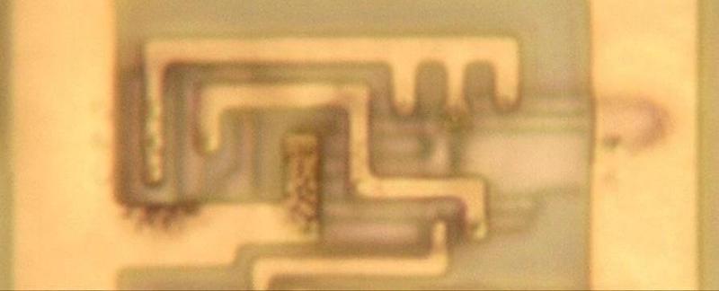
  9. The Pentium contains multiple types of BiCMOS standard cells, which I'll show in this footnote. The cell below is an inverter. It is similar to the BiCMOS buffer described earlier, except it lacks the first inverter in the circuit. To make room for the NPN transistor on the left, the PMOS transistors are shifted to the right. As a result, they don't line up with the PMOS transistors in other cells. This is a break from the traditional orderliness of standard cells.

    A BiCMOS inverter with PMOS on the left and NMOS on the right. The input is at the bottom and the output is in the middle.

    A BiCMOS inverter with PMOS on the left and NMOS on the right. The input is at the bottom and the output is in the middle.

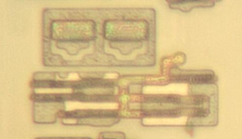
    The BiCMOS inverter below is similar, except it uses two NPN transistors, providing more output drive. I removed the M1 metal layer to provide a better view of the transistors.

    A BiCMOS inverter with two NPN transistors. The PMOS transistors are in the lower left and the NMOS transistors are in the lower right.

    A BiCMOS inverter with two NPN transistors. The PMOS transistors are in the lower left and the NMOS transistors are in the lower right.

    Another interesting BiCMOS circuit is the D flip-flop with enable and BiCMOS output, shown below. This is similar to the earlier flip-flop except it has an enable input, allowing it to either load a new value triggered by the clock, or to hold its earlier value. This allows the flip-flop to remember a value for more than one clock cycle. The additional functionality is implemented by another multiplexer, selecting either the old value or the new value. (This multiplexer is, in a way, one level higher than the multiplexer in each latch.) The transistor for the BiCMOS output is in the upper right, poking out from under the metal. (This circuit might be implemented as two independent cells, one for the flip-flop and one for the driver; I'm not sure.)

    A D flip-flop in the Pentium.

    A D flip-flop in the Pentium.


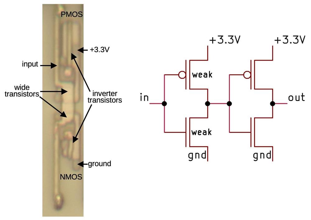
  10. One puzzling inverter variant is used in a gate I'll call the "slow buffer". This buffer consists of two inverters, so it passes its input through to the output, buffered. The strange part is that the first inverter uses transistors with wide gates, which makes these transistors much weaker than regular transistors. As a result, the first inverter will be slow to switch states. My guess is that this circuit is used to delay signals, for example, to keep a signal aligned with another signal that is delayed by multiple logic gates.

    The buffer consists of two inverters. The first inverter uses wide, weak transistors.

    The buffer consists of two inverters. The first inverter uses wide, weak transistors.

    You might expect that larger transistors would be stronger, not weaker. The problem is that these transistors are larger in the wrong dimension. If you make the gate wider, the effect is similar to multiple transistors in parallel, providing more current. But if you make the gate longer (as in this case), the effect is similar to multiple transistors in series, so the resistances add and the total current is reduced. In most cases, transistors are constructed with the smallest gate length possible, which is determined by the manufacturing process, so the transistors here are unusual. This chip was manufactured with an 800 nm process, so the smallest gate length is approximately 800 nm. The gate width (the normal direction for variation) varies dramatically depending on the circuit, optimized to provide maximum performance. 

Inside the tiny chip that powers Montreal subway tickets

To use the Montreal subway (the Métro), you tap a paper ticket against the turnstile and it opens. The ticket works through a system called NFC, but what's happening internally? How does the ticket work without a battery? How does it communicate with the turnstile? And how can it be so cheap that you can throw the ticket away after one use? To answer these questions, I opened up a ticket and examined the tiny chip inside.

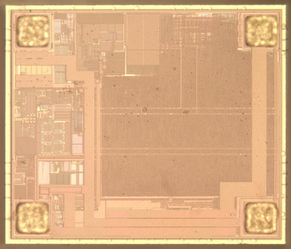
The image below shows the chip inside the ticket, highly magnified. The four golden squares in the corner are the connections to the antenna. The tan-colored lines are the metal wiring layer on top of the chip; the thickest lines wire the antenna to other parts of the chip. The darker region that takes up the majority of the chip is the chip's digital logic. To the left is the analog circuitry that handles the signal from the antenna.

The MIFARE Ultralight die under the microscope. (Click this image (or any other) for a larger view.

The MIFARE Ultralight die under the microscope. (Click this image (or any other) for a larger view.

The chip uses NFC (Near-Field Communication). The idea behind NFC is that a reader (i.e. the turnstile) and an NFC tag (i.e. the ticket) communicate over a short distance through magnetic fields, allowing them to exchange data. The reader generates a magnetic field that both powers the tag and sends data to the tag. Both the reader and the tag have coil-like antennas so the reader's magnetic field can be picked up by the tag.1 When you tap your ticket on the turnstile, the NFC communication happens in 35 milliseconds, faster than an eyeblink. The data provided by the NFC tag shows that you have a valid ticket and then you can enter the subway.

The photo below shows the subway ticket, made of printed paper.2 At the right, the ticket appears to have golden smart-card contacts, like a credit card with an EMV chip. However, those contacts are completely fake, just printed onto the card with ink, and there is no chip there. Presumably, the makers thought that making the card look like a smart card would help people understand it. The card actually uses an entirely different technology.

A Montreal subway card. This card is for occasional use and is disposable. Regular travel uses a rigid plastic card containing a different chip.

A Montreal subway card. This card is for occasional use and is disposable. Regular travel uses a rigid plastic card containing a different chip.

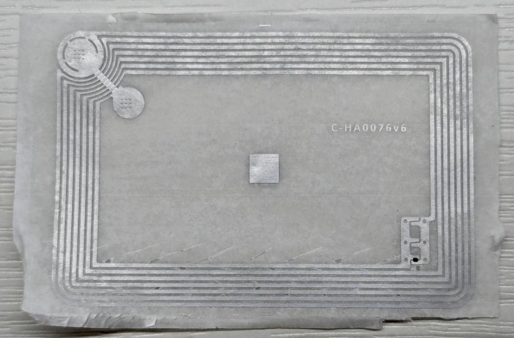
Although the subway card is paper on the outside, its core is a thin plastic sheet, shown below. The sheet has a coiled antenna made from a layer of metal foil. If you look closely, you can see the tiny NFC chip in the lower right, a black speck connected to two sides of the antenna wire.3 The diagonal metal stripe in the upper left makes the antenna into a loop; topologically, a spiral antenna won't work on a 2-D sheet, so the diagonal bridge completes the circuit.

The antenna and chip inside the subway card.

The antenna and chip inside the subway card.

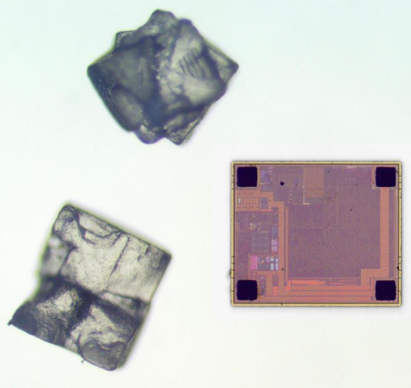
I want to emphasize the absurdly small size of the chip: 570 µm × 485 µm. The photo below shows that it is about the size of a grain of salt. The chip is also extremely thin—75 µm or 120 µm—so you can't even feel the chip inside the ticket.

The chip next to grains of salt. I composited two images, one illuminated from above to show the die and one illuminated from below to show the salt.

The chip next to grains of salt. I composited two images, one illuminated from above to show the die and one illuminated from below to show the salt.

Functions of the chip

There are many different types of NFC chips with varying levels of functionality. 4 This one is called the MIFARE Ultralight EV1,5 a low-cost chip designed for one-time ticketing applications. The basic function of the Ultralight chip is simple: providing a block of data to the reader. The chip holds its data in a small EEPROM; this chip has 48 bytes of user memory, while another variant has 108 bytes of user memory.

The Ultralight chip lacks the cryptography support found in more advanced chips. The Ultralight isn't much more secure than a printed ticket with a QR code or barcode, like you'd download for a show. It's up to the reader to validate the data and make sure the same ticket isn't being used multiple times.6

The Ultralight chip has a few features beyond a printed ticket, though. The chips are manufactured with a unique 7-byte identification code (UID). Moreover, the UID is signed, ensuring that fake UIDs cannot be generated.7 The chip also supports password-protected memory access and locking of memory pages to prevent modification. Since the password is transmitted without encryption, the security is weak, but better than nothing.8

Another interesting feature of the chip is the one-way counter. The chip has three 24-bit counters that can be incremented but not decremented. The counters can be used to allow the ticket to be used a particular number of times, for instance.9

Photographing the chip

To photograph the chip, I went through several steps to remove the chip from the ticket and then strip the chip down to the bare silicon. First, to extract the plastic sheet with the chip and the antenna from the paper ticket, I simply soaked the ticket in water. This turned the paper into mush, which could be scraped off to reveal the plastic core. Next, I cut out a small square of plastic that included the chip and put it in boiling sulfuric acid for about 30 seconds. This removed the plastic and adhesive, leaving the silicon die. (I try to avoid boiling acids, but processing a tiny chip like this only required a few drops of sulfuric acid, minimizing the risk.)

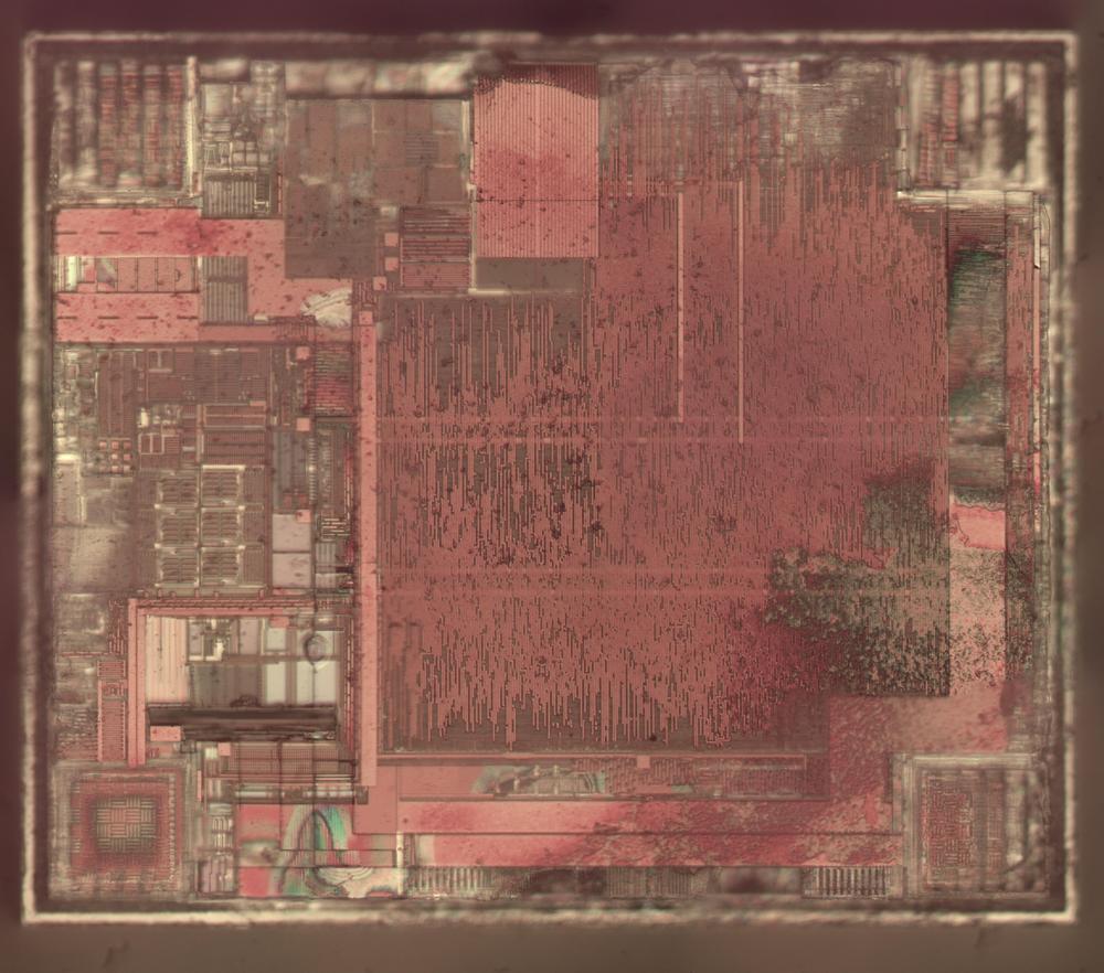
The die was covered with a passivation layer to protect its surface, a sandwich of silicon nitride and PSG (phosphosilicate glass) 1.1 µm thick according to the datasheet. The chip's underlying circuitry was visible, but slightly hazy due to this layer. I removed the passivation layer by boiling the chip in phosphoric acid for a few minutes. The image below shows the chip after this step. The top metal layer is much more visible, although some of the metal was dissolved by the acid. The thick metal lines connect the four bond pads to various parts of the analog circuitry, while many thin vertical metal lines provide interconnections of the logic circuitry.

The die after treatment with phosphoric acid to remove the passivation layer. Click for a much larger version.

The die after treatment with phosphoric acid to remove the passivation layer. Click for a much larger version.

Next, I treated the die with several cycles of treatment with Armour Etch to dissolve the oxide layer and hydrochloric acid to dissolve the metal. I think the chip had three layers of metal wiring on top of the silicon. Unfortunately, my process doesn't remove the metal layers cleanly, but causes them to come off in chaotic tangles. Since I wasn't interested in tracing the circuitry layer-by-layer, this wasn't a significant problem.

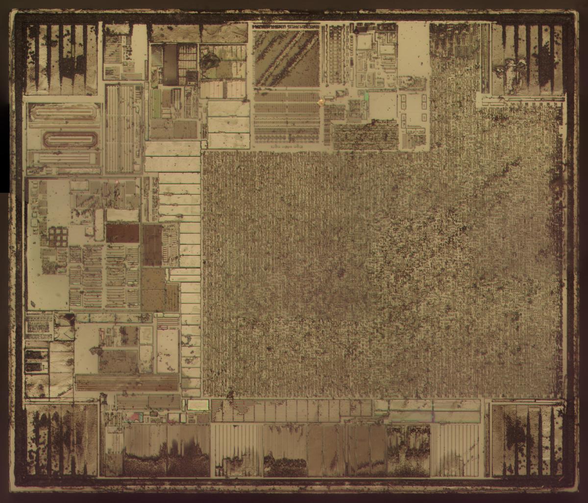
With the metal layers and polysilicon removed, I was left with the bare silicon. At this point, the underlying structure of the chip is visible. The doped silicon regions show the transistors, although they are extremely small at this scale. The white rectangles are capacitors. The chip has capacitors for many reasons: producing the right resonant frequency with the antenna, filtering the power, and boosting the voltage with charge pumps.

The die after stripping it down to the silicon.

The die after stripping it down to the silicon.

My biggest concern while processing this chip was to avoid losing it. With a chip this small, bumping the chip or even breathing on it can send the chip flying perhaps never to be seen again. Even trying to pick up the chip with tweezers is risky, since it can easily pop out and disappear. It's no fun examining the floor, inch by inch, trying to figure out if a speck is the lost chip or a bit of dirt. I found that the best way to move the chip between processing and a microscope slide was to put the chip in a few drops of water and move it with a pipette. Even so, there were a couple of times that I lost track of the chip and had to check some specks under the microscope to determine which was the chip and which were dirt.

Overview of the chip

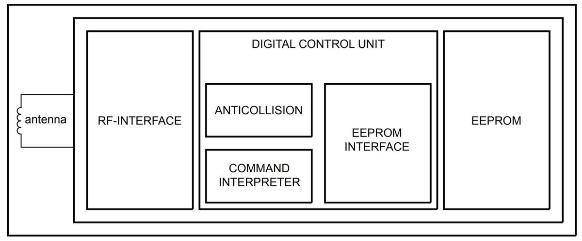
The block diagram below shows the high-level structure of the chip. At the left, the antenna is connected to the RF interface, the analog circuitry that converts the high-frequency signals into digital data. This circuitry also extracts power from the antenna's signal to power the chip.

Block diagram of the MIFARE Ultralight chip, from the datasheet.

Block diagram of the MIFARE Ultralight chip, from the datasheet.

The majority of the chip contains digital logic to process the 18 different commands that it can receive from the reader. Some commands, such as Wake-up or Halt control the chip's state. Other commands, such as Read or Write provide access to the EEPROM storage. The specialized Read_Cnt and Incr_Cnt commands access the chip's counters.

The chip has an "intelligent anticollision function" that allows multiple cards to be read without conflict if they are presented to the reader simultaneously. If a conflict is detected, the reader uses a standard NFC algorithm to select the cards one at a time, based on their identification numbers. The anticollision algorithm uses four of the chip's commands.

Finally, the chip has an EEPROM to store its data. Unlike RAM, the EEPROM holds data even when unpowered; it is designed to hold data for 10 years. To store data in the EEPROM, it must be written with a higher voltage than the rest of the chip uses. The EEPROM interface circuit produces the necessary signals.

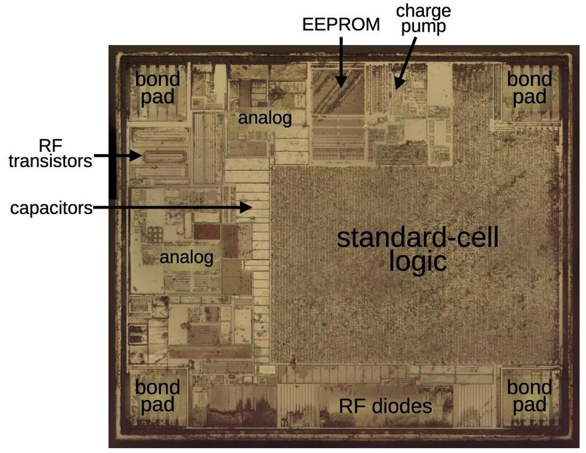
The diagram shows the chip with its functional blocks labeled. The majority of the die is occupied with digital logic; I'll explain below how it is implemented with standard-cell logic. At the top is the EEPROM, a square of storage cells. To the right of the EEPROM is a charge pump, a circuit to boost the voltage through switched capacitors. The EEPROM interface circuitry is between the EEPROM and the digital logic.

The die, stripped down to the silicon, with presumed functional blocks labeled.

The die, stripped down to the silicon, with presumed functional blocks labeled.

The remainder of the chip contains analog circuitry that is harder to interpret, so my labels are somewhat speculative. The four bond pads are where the antenna is connected to the chip. There are four pads to support two parallel antennas if desired. The first die photo shows the metal wiring between the bond pads and the structures that I've labeled as RF transistors and RF diodes. The "RF transistors" in the upper left are large, oval-shaped structures. These may be the transistors that send data back to the reader by modifying the load. Alternatively, they could be Zener diodes to regulate the voltage powering the chip, since Zener diodes often have an oval shape. The "RF diodes" at the bottom may rectify the signal from the antenna, producing the power for the chip. The rectified signal is also demodulated and processed by the analog logic to extract the digital data sent from the reader.

Sending data from the tag to the reader: load modulation

You might expect the tag to send data back to the receiver by transmitting a signal through the antenna. However, transmitting a signal takes power and the tag doesn't have much power available, just the power that it extracts from the reader's signal. Instead, the tag uses a clever technique called load modulation to send data to the reader. The idea is that if the tag changes the load across the antenna, it will absorb more or less energy from the reader. The reader can detect this change as a small variation in voltage across its transmitting antenna. Thus, the tag can dynamically change its load to send data back to the reader. Even though the signal produced by load modulation is extremely weak (80 dB less than the transmitted signal), the reader can detect it and extract the data.

In more detail, the reader transmits at a carrier frequency of 13.56 MHz.10 To send data back, the tag switches its load on and off at 848 kHz (1/16 of the carrier frequency), producing a subcarrier on top of the reader's signal. To transmit bits, this load modulation is switched on or off to transmit 106 kilobits per second (1/8 of the modulation frequency). The reader, in turn, extracts the subcarrier with a filter to receive the data bits from the tag.

An NFC tag can apply a load that is either a resistor or a capacitor; a resistor absorbs the signal directly, while a capacitor changes the antenna's resonant frequency and thus the amount of signal transferred to the tag. The die contains many capacitors, but I didn't see any significant resistors, so I suspect that this chip uses a capacitor for the load.

The chip's manufacturing process

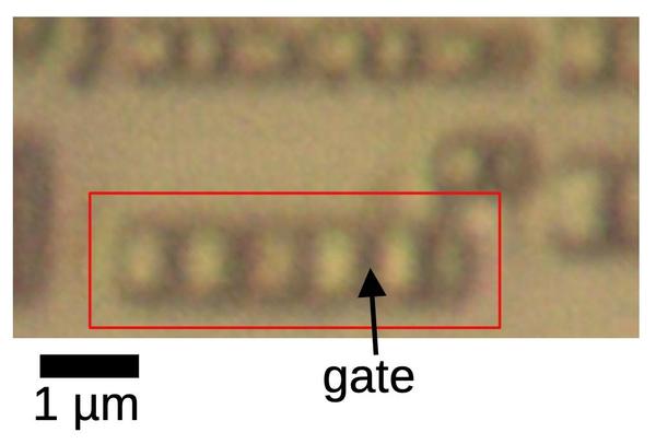
The image below shows an extreme closeup of the die. The red box surrounds a region of doped silicon, forming five MOS transistors in series. Each dark vertical line corresponds to the gate of one transistor so the width of this line corresponds to the feature size. I estimate that the chip's feature size is 180 nm. In comparison, the wavelength of visible light is 400-700 nm. Since the features are smaller than the wavelength of light, it's not surprising that image appears blurry.

A closeup of the die, pushing the limits of my microscope.

A closeup of the die, pushing the limits of my microscope.

The 180 nm process was popular in the late 1990s. These features are very large, however, compared to recent chips with features that are a few nanometers across. At the time the MIFARE Ultralight EV1 chip was released (October 2012), the newest semiconductor manufacturing process was 22 nm, so the 180 nm process they used was old even then.

However, it makes sense that the chip would be manufactured with an older process for several reasons. First, much of the chip's area is occupied by analog circuitry and the four bond pads, so shrinking the digital logic won't reduce the overall size much. Moreover, a significantly smaller chip would be impractical to attach to the antenna; I expect even the current chip is a pain to mount. Finally, this chip is designed for the extremely low-cost (i.e. disposable) market, so the chip is manufactured as inexpensively as possible. With a more modern process, more chips would fit on a wafer, dropping the price, but manufacturing each wafer would be more expensive, so there is a tradeoff.

Standard-cell logic

The chip's digital circuitry is implemented with standard-cell logic, a common way of implementing digital logic. The idea behind standard-cell logic is to use automated tools to create the chip layout from a description of the desired logic. The process starts with a library of standard cells. Each cell is a standardized implementation of a simple circuit such as a NAND gate or a flip-flop. The cells are designed so they have a fixed height and can be arranged in rows. The cells are then connected by metal wiring on top of the cells to produce the desired circuitry. Although the resulting circuitry isn't as dense and efficient as a fully customized and optimized layout, standard cell logic is much faster (and thus cheaper) to design than a hand-tuned layout. Thus, standard-cell logic has been heavily used for integrated circuit design since the 1980s.

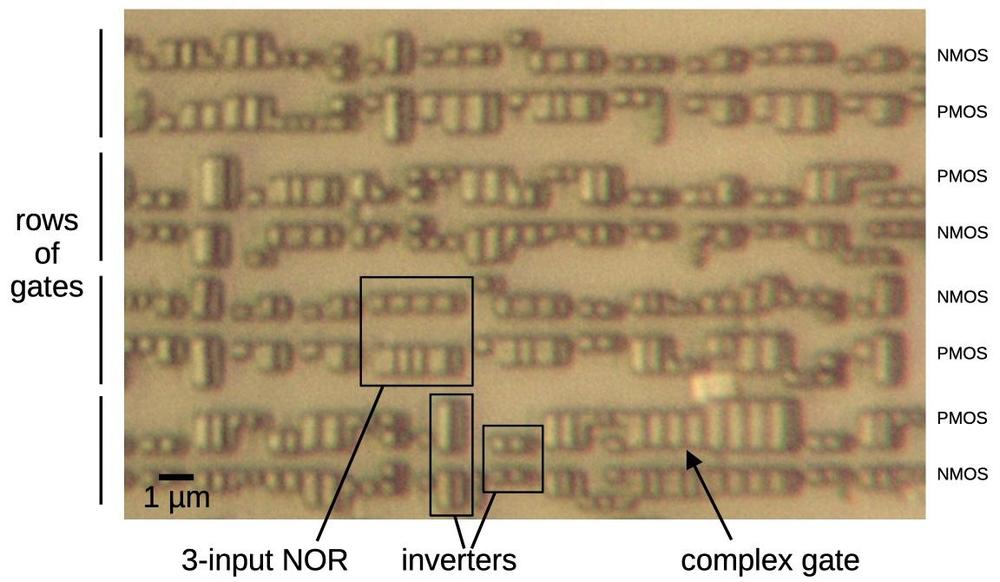
The photo below shows four rows of gates implemented with standard cell logic, The chip (like most modern chips) uses CMOS logic, with each logic gate built from two types of transistors: NMOS and PMOS. To simplify manufacturing, the NMOS and PMOS transistors are arranged in separate rows. Thus, each row of logic consists of a row of PMOS transistors on top and a row of NMOS transistors below, or vice versa. Due to the physics of semiconductors, the PMOS transistors are larger, which allows the transistor types to be distinguished in the image.

A closeup of the standard cell logic.

A closeup of the standard cell logic.

Looking at some of the cells and extrapolating, I estimate about 8000 gates in the logic section with about 45,000 transistors. One question is if the chip is implemented as a hardcoded state machine, or if it contains a processor (microcontroller). The transistor count is barely large enough to implement a simple microcontroller such as an 8051, but that wouldn't leave many transistors left over for other necessary circuitry. If a microcontroller were present, it would need software stored somewhere. Given the simplicity of the protocol and the relatively small number of transistors, my guess is that the chip is implemented in hardware (state machines and counters) rather than through a microcontroller.

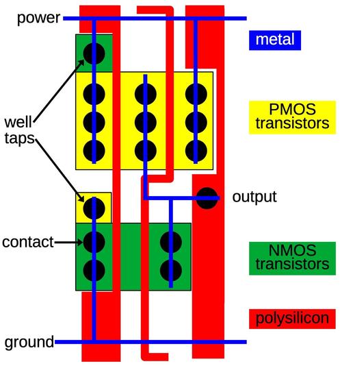
The diagram below shows how a standard cell implements a 2-input NAND. (This cell is from the Intel 386, not the NFC chip, but the structures are similar.) The cell contains four transistors. The yellow region is the P-type silicon that forms two PMOS transistors; the transistor gates are where the polysilicon (red) crosses the yellow region. (The middle yellow region is the drain for both transistors; there is no discrete boundary between the transistors.) Likewise, the two NMOS transistors are at the bottom, where the polysilicon (red) crosses the active silicon (green). The blue lines indicate the metal wiring for the cell. The black circles are contacts, connections between the metal and the silicon or polysilicon. Finally, the well taps are the opposite type of silicon, connected to the underlying silicon well or substrate to keep it at the proper voltage.

A standard cell for NAND in the Intel 386.

A standard cell for NAND in the Intel 386.

EEPROM

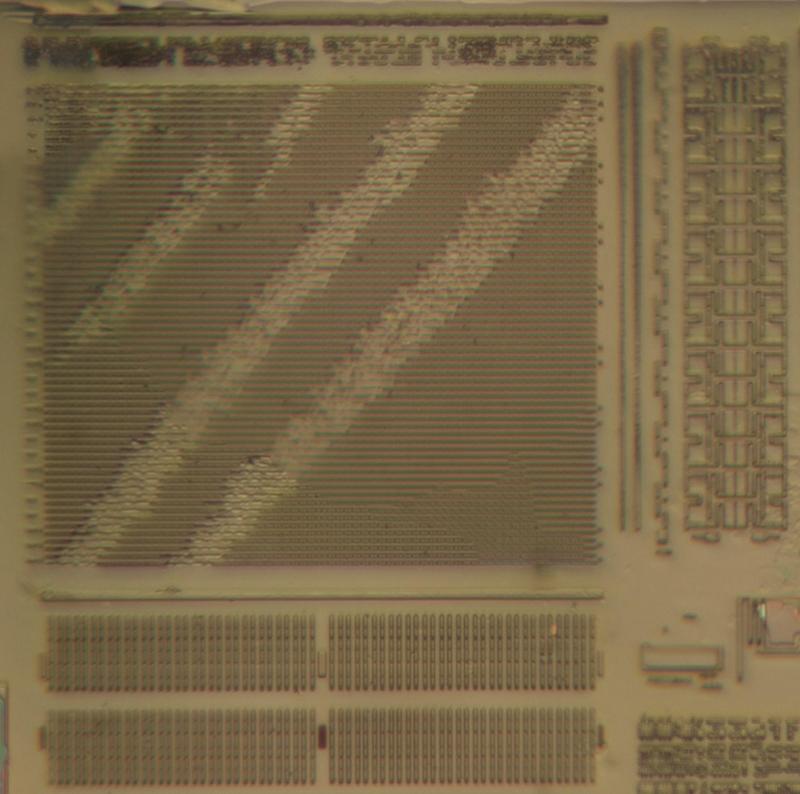
The chip stores its data in an EEPROM, similar to flash memory. The chip provides 640 or 1312 bits of EEPROM, based on the part number; I believe both versions use the same EEPROM implementation, but the cheaper version limits the amount that can be used. I think the EEPROM is the matrix shown below, with row and column drive circuitry to the right and below. (The diagonal lines are accidental scratches while I was processing the chip.)

A closeup of the presumed EEPROM circuitry on the die.

A closeup of the presumed EEPROM circuitry on the die.

In the photo, the EEPROM appears to be a 64×64 grid, 4K bits of storage rather than the advertised 1312 bits. There are several possible explanations. First, I could be miscounting the capacity (it is easy to be off by a factor of 2, depending on the cell structure). Second, the chip stores data that isn't reflected in the EEPROM memory map; for instance, the one-way counters and the UID signature are not included in the EEPROM storage count. Another possibility is that the extra EEPROM space holds code for a microcontroller (if the chip has one).

An EEPROM requires a relatively high voltage (10-20V) to force electrons into the storage cell for a bit. This voltage is generated by a charge pump circuit that switches capacitors at high frequency to boost the voltage. To the right of the EEPROM is a circuit with several large capacitors, presumably the charge pump.

Conclusions

It's remarkable that these NFC chips can be manufactured so cheaply that they are disposable. To keep the price down, the chips are sold by the wafer and then mounted in the tickets.11 You can buy an eight-inch silicon wafer with the chips for $9000 from Digikey. This may seem expensive until you realize that a single wafer provides an astonishing 100,587 chips, yielding a per-chip price of nine cents. According to the datasheet, a wafer has 103,682 potential good dies per wafer (PGDW). Some dies will be faulty, of course, so the wafer comes with a file telling you which dies are the good ones, 97% of them. (During the manufacturing of a typical chip, the faulty ones are marked with a spot of ink. But that won't work in this case since each die is much smaller than an ink spot.) If you need more chips, you can buy a 12" wafer for $19,000, providing 215,712 chips. A ticket manufacturer mounts each chip on an antenna sheet and then prints the ticket, adding a few cents to the cost of the ticket. The result is an inexpensive ticket that can be used once and discarded.

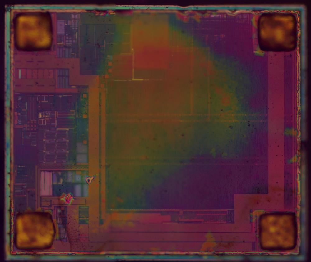
I'll leave you with one last die photo. In my first attempt at processing the chip, I treated it with Armour Etch. Although this failed to remove the passivation layer, it thinned it slightly, enough to generate some wild colors due to thin-film interference. I call this the "tie die".

The die after treatment with Armour Etch.

The die after treatment with Armour Etch.

Follow me on Twitter @kenshirriff or RSS for more. I'm also on Mastodon as oldbytes.space@kenshirriff. If you're interested in this type of chip, a few years ago, I looked at two RFID race timing chips, the Monza R4 and Monza R6.

Notes and references

  1. Because the card and the reader are positioned close together, the two antennas use "inductive coupling", coupled by magnetic fields rather than radio waves. That is, the two antennas act like transformer windings, transmitting the signal from the reader to the card. 

  2. The Montreal subway uses multiple types of cards. In this blog post, I examine the Occasional card (L'Occasionnelle). This is a non-rechargeable card that works for a single trip or up to three days, and then is discarded. For long-term usage, Montreal uses the Opus card, which provides more security and implements the Calypso standard. An Opus card is plastic rather than paper, giving it a longer life. The Calypso standard is much more secure, using cryptography such as AES, DES, and ECC (spec) and provides much larger EEPROM storage. Thus, the transit system uses the Occasional card for cheap, disposable tickets and the Opus card for a long-term ticket, where spending a dollar or two on the physical card isn't an issue.

    I haven't examined an Opus card, so I don't know what type of chip it uses or even who manufactures the chip. Many companies produce Calypso cards, for instance, the STMicroelectronics CD21 Calypso chip is based on an Arm core. 

  3. If you look closely at the lower right corner of the NFC card, it has three positions that can hold a chip, with the chip in position #3. Presumably, this allows three different NFC chips to be mounted in one card, so one card could have three functions. The NFC protocol is designed to avoid collisions if multiple chips respond, so the three chips won't interfere with each other. 

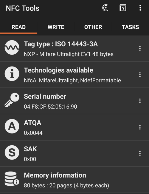
  4. You can easily examine NFC cards like this using your phone, with an app such as NFC Tools or NXP's Taginfo. Tapping a card will display the type of the card and allow the memory to be read (subject to security restrictions). It's entertaining to tap various NFC cards and see what type of chip they use; I found that hotels typically use the MIFARE Classic chip, more advanced than the MIFARE Ultralight chip in the subway ticket.

    The NFC Tools app shows that this card is a MIFARE Ultralight EV1.

    The NFC Tools app shows that this card is a MIFARE Ultralight EV1.


  5. The part number, as provided by the chip, is MF0UL1101DUx. "MF0UL" indicates the MIFARE Ultralight EV1, a chip in the Ultralight family manufactured by NXP. An "H" if present indicates 50 pF input capacitance, rather than 17 pF in the chip I examined, allowing a different antenna. Next, "1" indicates a chip with 384 bits of user memory, while "2" would indicate 1024 bits. This is followed by "101D", and then a code indicating the specific package: "U" indicates a wafer, while "A" indicates a plastic leadless module carrier (LCC). Other characters specify the wafer diameter and thickness. 

  6. It is instructive to think about the security of a printed ticket for a concert with a barcode. You could print out a hundred copies of the ticket, but it will only get you into the concert once. (This assumes that the venue has a centralized database so they can keep track of which tickets have been scanned.) Most of the security is implemented in the backend system, not the ticket itself. The ticket numbers need to be unforgeable, either by generating random numbers or using cryptography. (If the tickets just have QR codes with the numbers 1 to 100, for instance, it would be trivial to make fake tickets.) Moreover, there is nothing to ensure that the person scanning the ticket is legitimate; someone malicious could scan your ticket in line, print out a copy, and get into the concert instead of you. The MIFARE Ultralight chip is similar to a paper ticket in many ways with only slightly more security. 

  7. The UID signing is done with an ECC (elliptic-curve cryptography) algorithm. Note that the chip doesn't need any cryptographic support for this; the chip just holds the signature that was programmed during manufacturing. As far as the chip is concerned, it is just providing some stored bytes. 

  8. The MIFARE Ultralight has enough security to work as a limited-use ticket, but more advanced applications such as reloadable stored-value cards require a chip that supports encryption such as the DESFire. This allows the market to be partitioned, with the inexpensive Ultralight supporting the low-end market, while the more costly DESFire is required for more advanced applications.

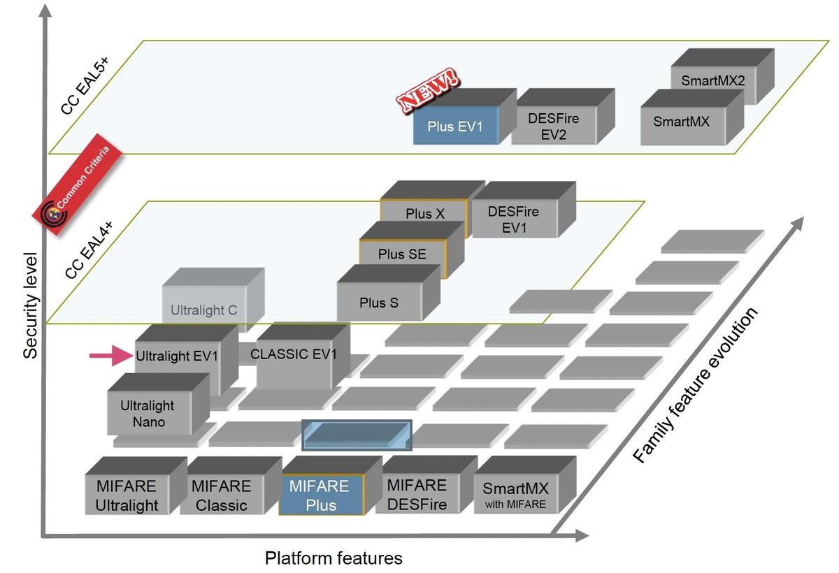
    There are many types of MIFARE cards and it's hard to keep them straight, but the diagram below from NXP may help. The different families are arranged left to right: Ultralight, Classic, Plus, DESFire, and SmartMX. The Y dimension indicates the official security certification level. The Z dimension (front to back) shows the evolution within a family over time. I've added a red arrow to indicate the "Ultralight EV1" chip, the focus of this blog post. (Personally, if you need a three-dimensional diagram to explain your product line, the product line may be excessively complicated.)

    The various MIFARE NFC types. Diagram from aMIFARE Plus Product Family.

    The various MIFARE NFC types. Diagram from aMIFARE Plus Product Family.


  9. In more detail, a 3-byte counter can be incremented by a specified value until it reaches the all-1's state (0xFFFFFF), at which point it stops. If you wanted to allow, say, 5 uses of a ticket, you could initialize the counter to all-1's minus 5. Then the counter could be incremented 5 times before reaching the limit.

    One complication is that the counters have an "anti-tearing" feature for additional security. The problem is that if you tear the card away from the reader in the middle of an update, there is a possibility for counters to be partially updated, yielding a bad result. The anti-tearing feature ensures that a counter will be atomically updated, avoiding a partial update. 

  10. There are multiple NFC standards with differences in speed, protocol, and range, including NFC-A, NFC-B, NFC-C, NFC-F, and NFC-V. The MIFARE Ultralight cards use NFC-A, which is defined by the standard "ISO/IEC 14443 Type A". Annoyingly, each part of the standard costs $70. The NFC Forum Analog Technical Specification provides a lot of detail, though. 

  11. Instead of a wafer, you can buy the chips on tape but it costs more than twice as much. 

Inside a vintage aerospace navigation computer of uncertain purpose

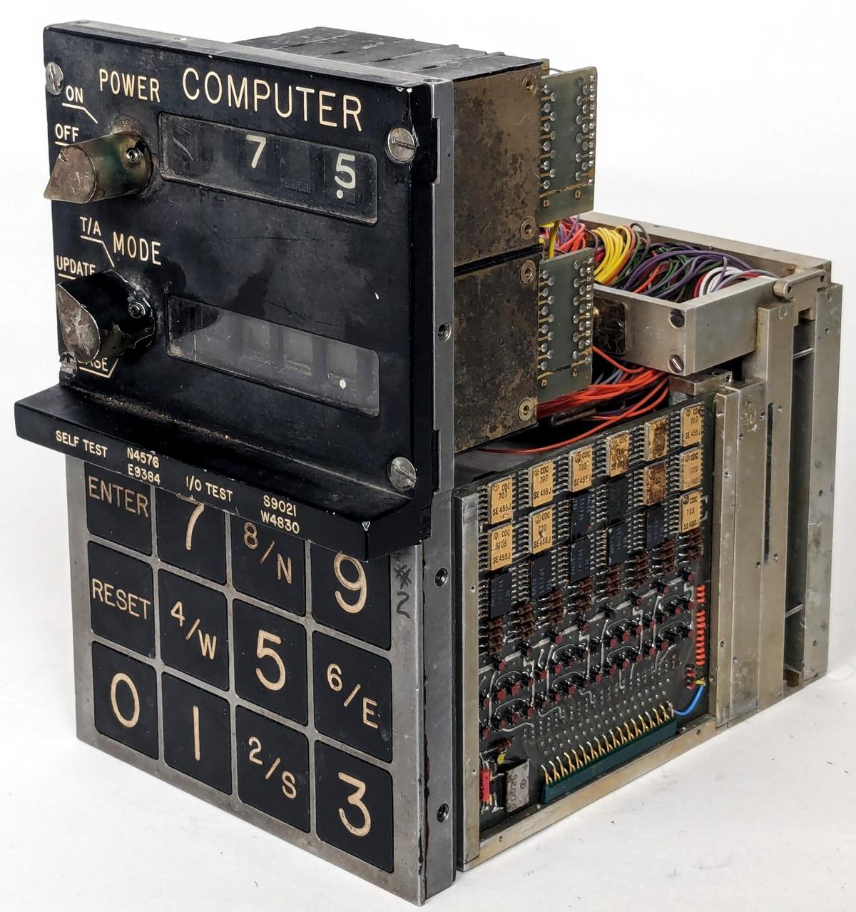
I recently obtained an aerospace computer from the early 1970s, apparently part of a navigation system. Aerospace computers are an interesting but mostly neglected area of computer hardware, so I'm always delighted to examine one up close. In an era when most computers were large mainframes, aerospace computers packed dense electronics into a small package, using technologies such as surface-mounted components and multi-layer printed circuit boards, technologies that wouldn't reach the mainstream for another decade. This blog post examines the circuitry and components inside this computer, including an unusual electromechanical display. Although I was unable to determine who manufactured this system or even its exact function, this system illustrates how hundreds of integrated circuits and a core memory stack can be crammed into a compact package.

The navigation computer, showing the front panel with the display and keyboard, with the electronics unit behind it. Click this image (or any other) for a larger version.

The navigation computer, showing the front panel with the display and keyboard, with the electronics unit behind it. Click this image (or any other) for a larger version.

The keyboard

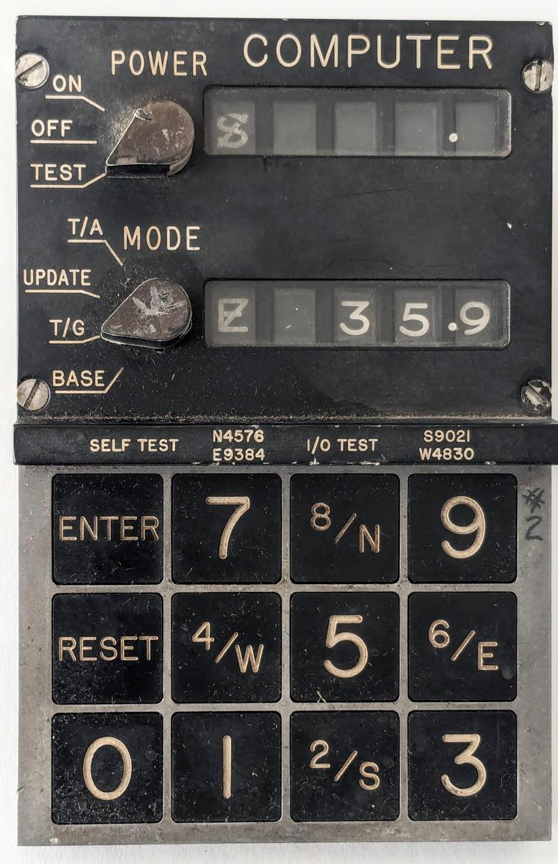
The device has a simple numeric keyboard with a few unexpected features. The numeric keypad can also be used for direction entry, as four of the keys have N, S, E, and W on them. The keys are large, roughly the size of the Apollo spacecraft's DSKY buttons. My theory is that these buttons are designed for operation with gloves, perhaps in a fighter plane where the pilot wears a pressure suit. The buttons are hinged at the top, so they don't push straight in, but pivot when pressed.

Numeric keypads typically use one of two layouts: a telephone-style keypad has the digits 123 at the top, while a calculator-style keypad has the digits 789 at the top. Interestingly, this device uses a calculator layout, while most aviation devices have a telephone layout. The Apollo DSKY also used a calculator layout, which could be a hint at a NASA connection for this device.

Above the keyboard are four codes for self-test: N4576, E9384, S9021, and W4830. Entering these codes on the keyboard presumably triggered the appropriate test of the system when the switch is in test mode.

The display

The computer's display is simple, showing a latitude and longitude. Each value has one decimal position, providing 0.1° of accuracy. The latitude and longitude are prefixed with a compass direction: North/South for latitude and East/West for longitude.

The front panel of the navigation computer, with a display and keyboard.

The front panel of the navigation computer, with a display and keyboard.

The display is constructed from an unusual type of electromechanical indicator, with an indicator module for each digit. Each digit position has a rotating wheel with 11 positions (ten digits and a blank). When the indicator module for a position is energized, the wheel spins to the specified position, showing the selected digit. The two leftmost indicators are slightly different as they show a compass direction instead of a digit: N, S, E, or W. Moreover, the direction indicators can also show the compass direction with a diagonal slash through it, as seen above. Perhaps the slashed direction indicates a problem with the value.

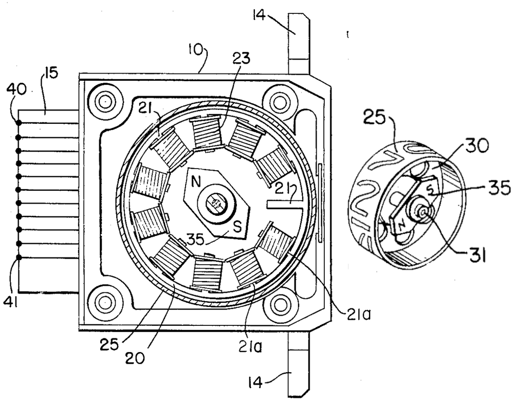
The diagram below shows how a digit indicator operates. Each digit position has an electromagnet with a wire to energize it. The dial wheel has an attached permanent magnet (indicated by N and S). Energizing one of the electromagnets causes the dial to spin to that position, aligning the permanent magnet on the dial with the electromagnet. This mechanism forms a reliable indicator with just one moving part. The displayed digit is clearer than a seven-segment display since the digit uses a real font rather than being created from segments.

A diagram illustrating the magnetic indicator construction. From Patent 3201785. The patent describes a different indicator but the construction is similar.

A diagram illustrating the magnetic indicator construction. From Patent 3201785. The patent describes a different indicator but the construction is similar.

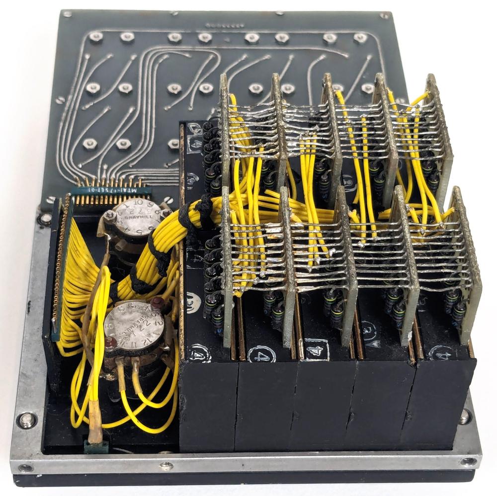
Looking at the back of the keyboard/display unit shows the wiring of the display indicators. Each indicator has a common connection and ten wires to energize one of the electromagnets.1 The electromagnets are connected in a matrix, with all the "1" wires connected, the "2" wires connected, and so forth. To rotate an indicator to a particular digit, a common wire and an electromagnet wire are energized. For instance, powering the common wire of the second indicator and the "5" electromagnetic wire causes the second indicator to rotate to the "5" position. The wiring has a three-dimensional structure with ten bare wires running between the boards, one for each digit value. A yellow wire hangs off each bare wire, linking it to the connector on the left. Each indicator has ten diodes on a circuit board to block "sneak" paths that would energize unselected electromagnets.

The back of the keyboard/display unit. The keyboard buttons are at the back of this photo, while the display modules are at the front.

The back of the keyboard/display unit. The keyboard buttons are at the back of this photo, while the display modules are at the front.

This matrix circuit reduces the amount of wiring required: although there are 100 electromagnets in total, just 20 wires are sufficient to control them. The driver circuitry, however, is a bit more complex as it must scan through the ten digit positions, activating the right pair of driver wires at the right time. Some of the logic circuitry described below must implement this scanning, as well as the driver circuitry to energize the indicators.

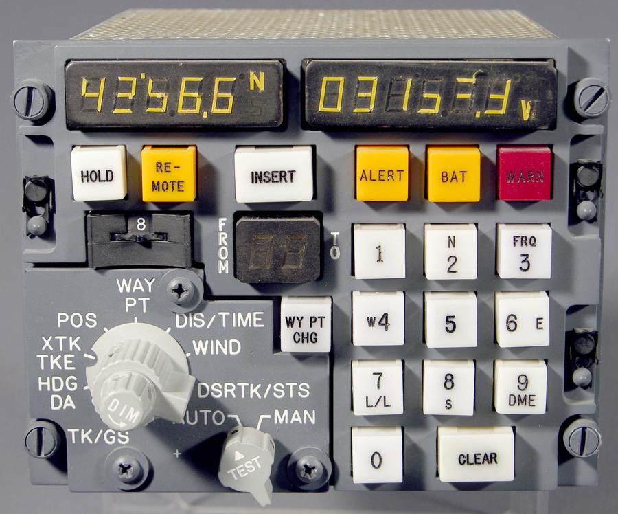
The display and keyboard have many similarities to the Delco Carousel Inertial Navigation System (INS) shown below. (The Delco Carousel was used in many military and civilian aircraft, from the C-141 cargo plane to the Boeing 747 passenger plane.) Both devices have two digital displays, one for latitude North/South and one for longitude East/West. Also note the numeric keypads with four keys assigned to the four compass directions. The controls of the Carousel INS system are considerably more complicated, though. The Carousel has a knob position "TK/GS" (track/ground speed), which may correspond to the "T/G" position on my device.

Control unit for the Delco Carousel inertial navigation system. From Smithsonian collection, gift of Delphi Electronics & Safety.

Control unit for the Delco Carousel inertial navigation system. From Smithsonian collection, gift of Delphi Electronics & Safety.

Note that the display on my unit has just four digits of accuracy, with one digit after the decimal point. A tenth of a degree would provide an accuracy of about ±7 miles, which is low for a navigation device. In comparison, the Delco Carousel has six digits of accuracy (± 100 feet perhaps). This suggests that the device does not provide INS navigation, but some other guidance with lower accuracy.

Packaging the electronics

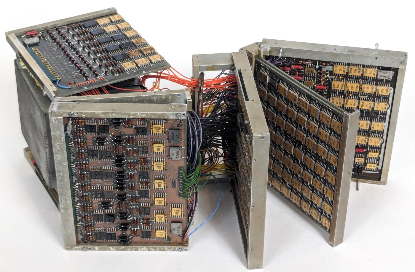
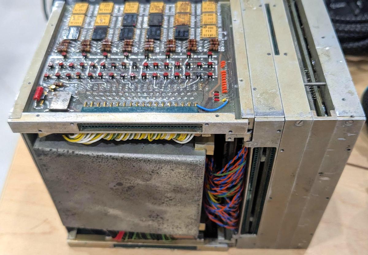
The unit contains 14 circuit boards, crammed with TTL integrated circuits, along with a core memory stack. The photo below shows how circuit boards surround the core memory stack. The mechanical design of the unit is advanced, allowing the boards to be opened up like a book. This provides compact packaging while allowing access to the boards.

The electronics unit can be disassembled and folds open like a book.

The electronics unit can be disassembled and folds open like a book.

The circuit boards are four-layer printed circuit boards, more advanced than the common two-layer boards of the time. The boards use a mixture of surface-mounted and through-hole components. The flat-pack ICs and the tiny round transistors are surface mounted, which was rare at the time. On the other hand, the resistors, capacitors, diodes, and larger transistors use standard through-hole components. At the time, most electronics used through-hole components, although aerospace systems often used surface-mounted components for higher density. It wasn't until the late 1980s that surface-mount technology became commonplace.

The boards are mounted in solid metal frames, providing both structural integrity and heat conduction for cooling. Most of the frames hold two boards, mounted back-to-back for higher density.

The logic boards

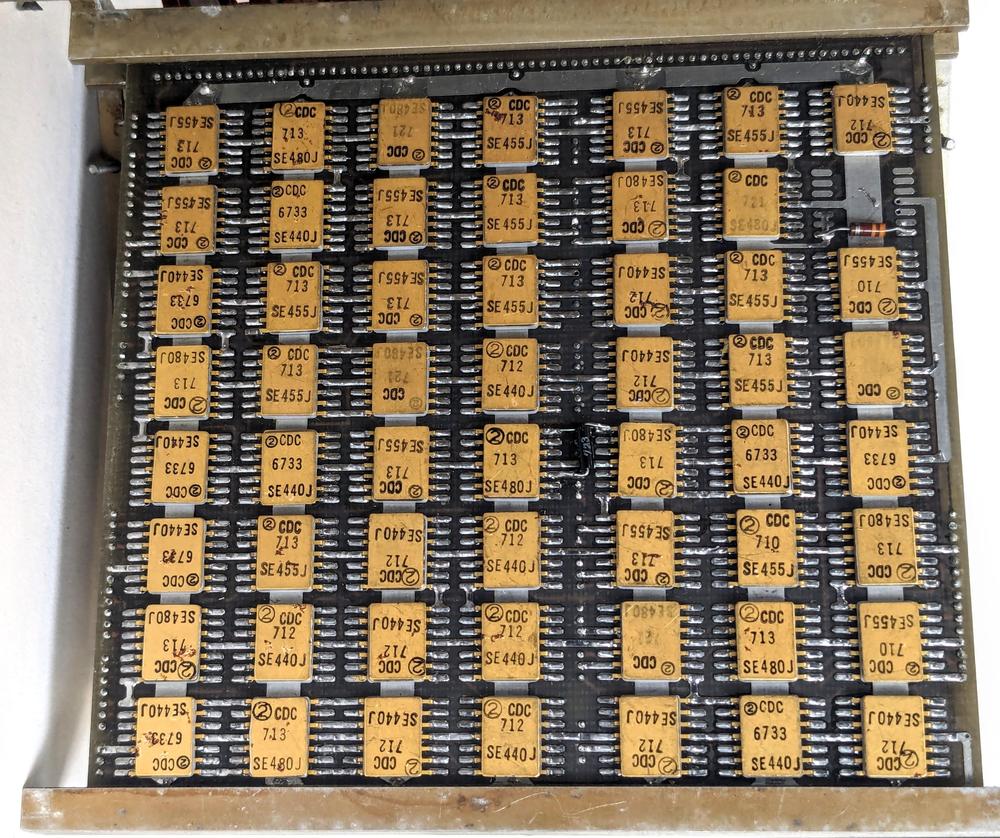
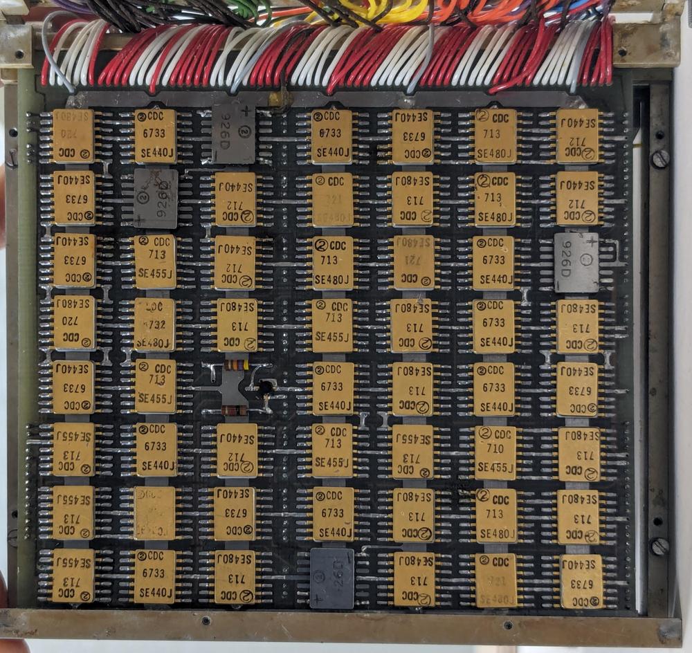
Four of the circuit boards are logic boards, packed with flat-pack integrated circuits. The board below holds 55 integrated circuits, showing the high density that is possible with flat packs.

A board filled with flat-pack logic ICs.

A board filled with flat-pack logic ICs.

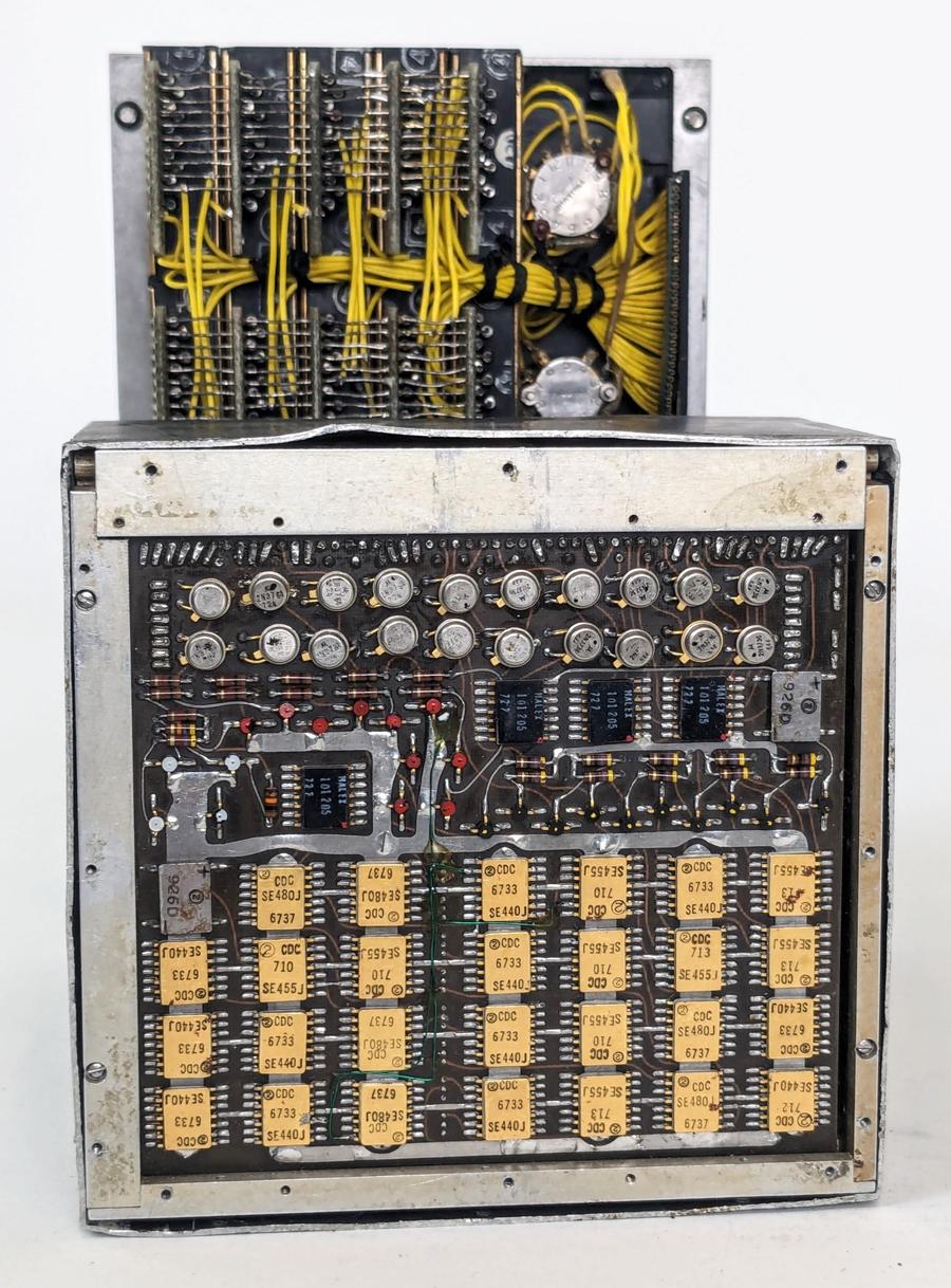
The logic ICs are Signetics 400-series chips, an early type of TTL (Transistor-Transistor Logic) chip. Just three types of these ICs are used: SE440J "Dual exclusive OR" (really AND-OR-INVERT but XOR if provided with particular inputs), SE455J "Dual 4-input buffer/driver" (4-input NAND or NOR gates depending on polarity), and SE480J "Quad 2-input NAND/NOR". These integrated circuits cost $15.45 each in 1966 (about $150 each in current dollars).2

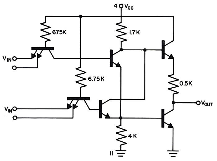
The schematic below shows the circuit that implements AND-OR-INVERT (or exclusive or) in the SE440J. The multiple-emitter transistors on the inputs may appear unusual, but this is the standard way to implement TTL gates. It is important to note that this chip only contains 12 transistors, so the density is low. (Since the chip contains two of these gates, this circuit is duplicated.) In the mid-1960s, integrated circuits only contained a few transistors—the Apollo Guidance Computer's ICs had just 6 transistors—but by the time this unit was built in the early 1970s, some chips had thousands of transistors, tracking Moore's Law. Thus, this unit both illustrates how aviation computers could be built from simple integrated circuits and how the dramatic improvements in IC technology rapidly obsoleted these computers.

Schematic of the SE440J integrated circuit. From datasheet.

Schematic of the SE440J integrated circuit. From datasheet.

The Signetics 400-series seems to have been obscure and short-lived, probably killed off by the wild success of 7400-series TTL chips. I was able to find only a few announcements and datasheets for these chips. The only users of these chips that I could find were NASA projects from the late 1960s.3 Signetics 400-series chips were used in the Mariner Mars and Venus probes, in the Data Automation Subsystem (DAS) (link, link). The Voyager Mars probes also used them. The SE455J gates were also used to interface the Apollo Guidance Computer to a core-rope simulator. JPL used the SE455J in a core memory system. NASA used the SE455J, SE480J, and other Signetics chips in its design for the MICROMIN computer. None of these systems appear to be related to the navigation system, but they illustrate that NASA was using these specific Signetics chips at the time in multiple designs.

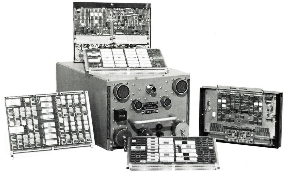
The chips are labeled "CDC", raising the possibility that these chips were built by Control Data Corporation (CDC) under license from Signetics. The Aerospace Division of CDC was active at the time, building various compact computer systems. For instance, the CDC 480 computer (1976) was a 16-bit computer based on the Am2900 bit-slice chip. Also known as the AN/AYK-14, this system was used on numerous aircraft including the F-18. An earlier CDC aerospace computer is the AN/AWG-9 Airborne Missile Control System (1965), a 24-bit computer in a compact 1.1 cubic foot package. Used on the F-14 fighter plane, this computer guided the Phoenix air-to-air missile. Based on CDC's activity in aerospace computers at the time, the mystery computer could be a CDC system, although this hypothesis is based solely on integrated circuits labeled "CDC".

The CDC AN/AYK-14 computer with circuit boards. This is an example of an aerospace computer built by CDC slightly later than the mystery computer. From a 1983 brochure.

The CDC AN/AYK-14 computer with circuit boards. This is an example of an aerospace computer built by CDC slightly later than the mystery computer. From a 1983 brochure.

The photo below shows another logic board. This one has numerous red and white wires attached, linking it to the rest of the system. Curiously, this board has a single transistor, with two associated resistors, in the middle of the board.

Another logic board, with a similar grid of flat-pack integrated circuits.

Another logic board, with a similar grid of flat-pack integrated circuits.

Analog boards

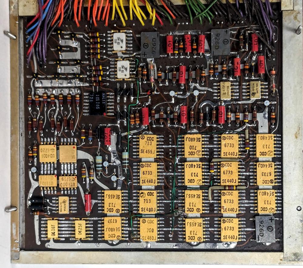
The computer contains not only logic boards but also boards full of analog circuitry to interface with the core memory, keyboard, and display. The board below contains 17 of the logic ICs seen earlier. However, it also uses many resistors, capacitors (red cylinders), transistors (white circles), inductors (white banded cylinders), and glass diodes. The board also has some analog integrated circuits. In particular, it has three TI SN52709 op-amps, the smaller 10-pin packages. The board also contains some integrated circuits that I couldn't identify: UT1000, UT1027, UD4001, and D245F. The SM 60 ICs in white packages have a logo that I don't recognize. The op-amps could function as sense amplifiers for the core memory, or this board could provide other analog interfacing.

A board with some analog integrated circuits.

A board with some analog integrated circuits.

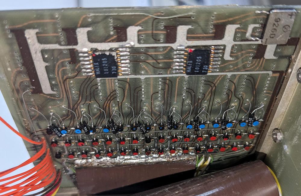
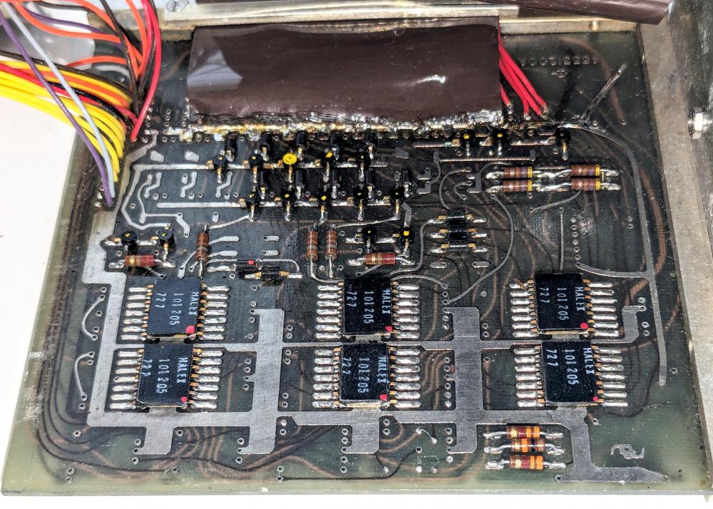
The board has multiple gray four-pin packages labeled "926D". Based on the + and - markings, these packages are probably bridge rectifiers, maybe providing power for the circuits. Many of the other boards have these rectifiers. The analog boards also contain a few Halex flat-pack devices labeled "HALEX 101205 727". Hanlex manufactured thin-film resistors in flat packs, so these are probably resistor networks. NASA used Halex resistor networks in some devices (link).4

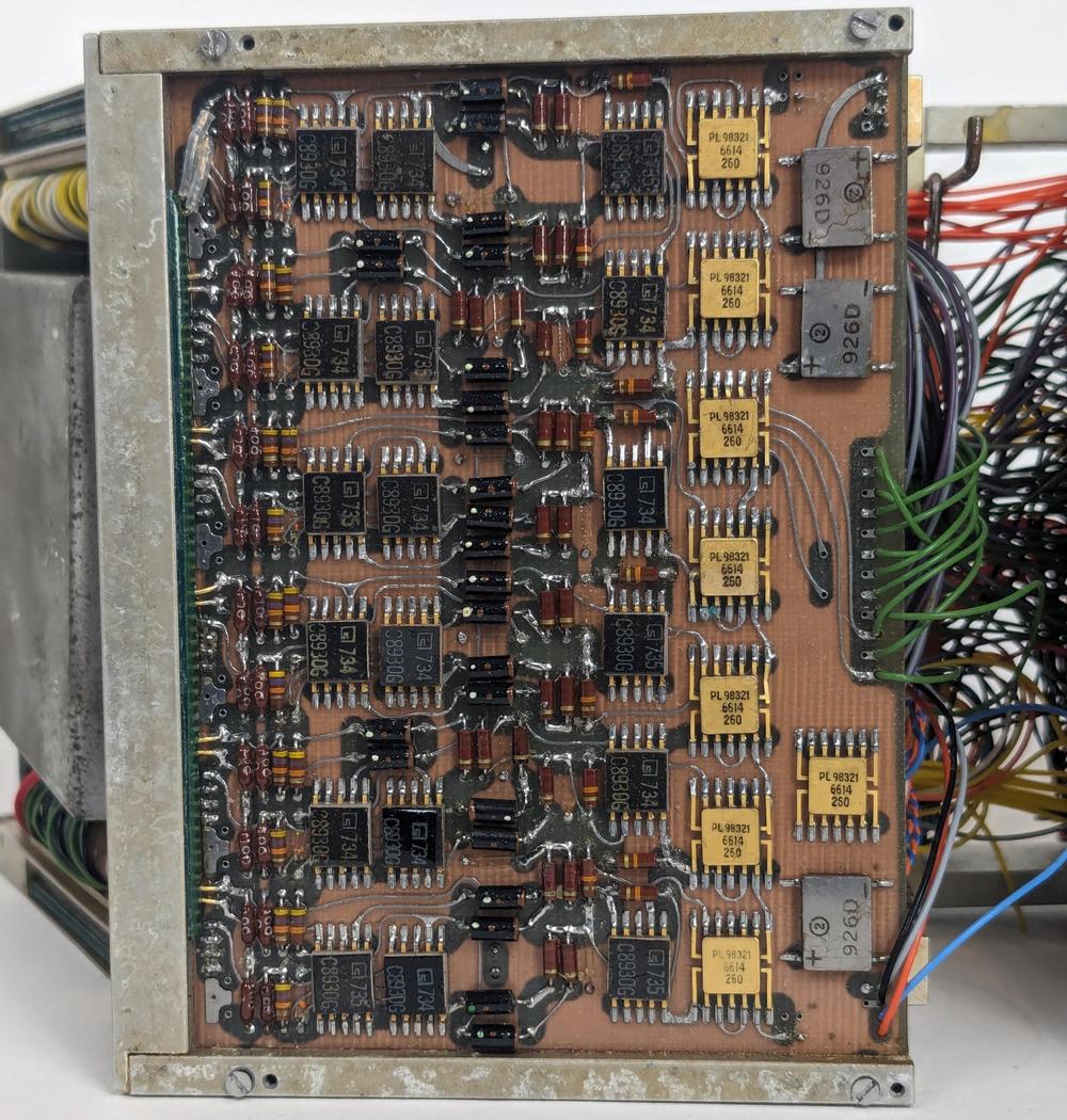
The analog board shown below sits next to the core memory stack. It uses a different set of flat-pack components: Signetics C8930G and PL 98321. Unfortunately, I could not identify these ICs. This board, unlike the previous boards, has a copper ground plane in the second layer of the circuit board; this layer is visible in the photo as the copper-colored background occupying most of the board.

Another analog board in the aviation computer.

Another analog board in the aviation computer.

Core memory

The unit is built around a core memory stack, as was common in the era before semiconductor memory took over. Magnetic core memory consists of a grid of tiny ferrite cores with wires threaded through them, forming a core plane. Typically, a core memory unit consists of multiple planes, one for each bit in the word, stacked to form a three-dimensional block of memory.

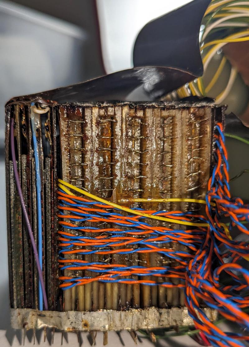
The photo below shows a closeup of the stack. It appears to have 20 planes, suggesting a 20-bit processor. Soldered wires connect the planes together to provide continuous wiring through the stack. The soldering on these wires looks somewhat haphazard, suggesting that this was not a production unit.

A closeup of the core memory stack. Brightly colored wires connect the module to the rest of the system. Small wires connect the layers together.

A closeup of the core memory stack. Brightly colored wires connect the module to the rest of the system. Small wires connect the layers together.

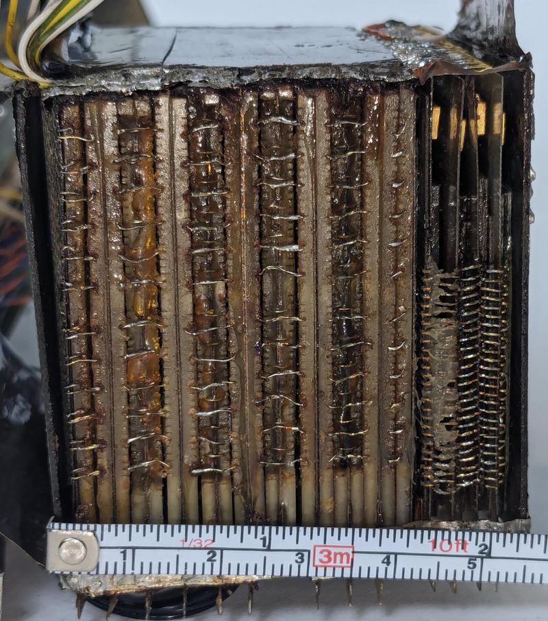
The photo below shows the other side of the core memory stack, with similar wiring between the planes. At the right are a few layers of a different type, connected with 26 wires. The tape measure shows that the core memory stack is compact, about 6 cm on a side (2¼").

Measurement of the core memory stack.

Measurement of the core memory stack.

Some of the boards are drivers for the core memory stack. The board below has 48 small round transistors, colored either blue or red. Note the green, white, and yellow wires in the lower right, mostly hidden under the brown ground ribbon. These wires are connected to the core memory stack.

A circuit board with many small transistors.

A circuit board with many small transistors.

The board below also has numerous wires to the core stack, underneath the brown ground ribbon, so it is presumably another driver board. This board has some round driver transistors with yellow dots. Curiously, in the upper left there are a few circuit board pads where transistors could be mounted but are missing. Perhaps with the additional components the board would support a system with more of something: a larger keyboard? more memory?

A board with driver transistors.

A board with driver transistors.

Looking at the back of the unit, you can see the display indicator wiring at the top and a circuit board at the bottom. This board contains 20 transistors in metal cans, specifically Motorola 2N3736 NPN transistors. The core memory stack has 20 planes, matching the 20 transistors on this board, so the board probably implements the core memory "inhibit drivers", controlling the bit written to each plane. The board also has numerous tiny surface-mount transistors in white, red, and black packages. Close examination shows a few thin green "bodge" wires on this board, indicating that rework was performed on the board to fix a circuit problem, another piece of evidence that this unit is a prototype.

A view of the computer from the back, showing the display wiring and a circuit board.

A view of the computer from the back, showing the display wiring and a circuit board.

The core memory stack is enclosed by two sheet metal boxes, which I removed for the photos. The stack also has two flexible ground planes attached to it. The designers clearly wanted to ensure that the memory was well shielded, to a degree that I haven't seen in other systems.

Conclusions

Despite my research, this aerospace computer remains a mystery. I was unable to identify who manufactured it or even its exact function. One hypothesis is a NASA connection since NASA was extensively using these Signetics chips at the time. Moreover, this computer was obtained in the Houston area. Another hypothesis, based on the "CDC" label on the chips, is that this computer was built by Control Data's Aerospace Division. If you have any leads on this mysterious aviation computer, please contact me.

This system may have been a prototype. It has no part numbers, manufacturer name, or identifying plate.5 Moreover, the soldering on the core memory stack doesn't seem to be flight quality. Finally, the boards don't have conformal coating, which is typically used for spaceflight systems. However, the mechanical design looks advanced for a prototype, with dense boards that fold together like a book.

This unit clearly has a navigation role, but seems to be too inaccurate for an inertial navigation system (INS). It contains many integrated circuits, but not enough to form a full computer. I hypothesize that this unit contains the circuitry to drive the core memory and the display, and handle keyboard input. Looking at the underside of the unit (below), there are three connectors. I suspect these connectors were plugged into a larger box that held the computer itself.

A view of the underside of the electronics unit with the core memory wrapped in sheet metal.

A view of the underside of the electronics unit with the core memory wrapped in sheet metal.

The date codes on the integrated circuits range from 1966 to 1973, so the computer was probably manufactured in 1973. The seven-year range for date codes is a bit surprising, since integrated circuit technology changed a lot during these years. I suspect that the Signetics 400-series ICs had older date codes because this line didn't catch on so there was a lot of old stock rather than newly-manufactured parts. I also suspect that this system was designed around 1969, based on the multiple NASA systems using these chips then, suggesting that the design and manufacturing of this unit was a multi-year project.

Despite the lingering mysteries of this device, it provides an interesting example of aerospace computers at the beginning of the 1970s. Even though integrated circuits were primitive at the time, with just a few transistors per chip, aerospace computers used these chips and high-density packaging to build computers that were compact, reliable, and low power. These miniature computers controlled aircraft, missiles, and spacecraft, worlds away from the room-filling mainframes that attracted most of the attention.

Thanks to Usagi Electric for providing the aerospace computer. Eric Schlaepfer and Marc Verdiell helped with the analysis. Thanks to Don Straney for his research and comments. Various commenters on Reddit and Twitter provided suggestions. Follow me on Twitter @kenshirriff or RSS for updates. I'm also on Mastodon as oldbytes.space@kenshirriff.

Notes and references

  1. The indicators have a blank position, so there are 11 electromagnets. However, only the ten electromagnets associated with digits are used in the device. The N/S/E/W indicators have a square box in one of the positions, which probably is not used. 

  2. Signetics had multiple temperature ranges for the 400-series low-power ICs. The RE prefix indicated ultra high reliability aerospace components rated for a temperature range of -55°C to +125°C. The SE prefix on the chips in this unit indicated military airborne chips with the same temperature range. A NE or ST prefix indicated military prototype or industrial chips with a smaller temperature range (0°C to +70°C). A SP prefix indicated the commercial temperature rating, from +15°C to +55°C. A J suffix indicated a flat pack and an A suffix indicated a dual in-line pack (DIP). 

  3. NASA computers are the only documented systems that I could find that used these Signetics chips. One possible conclusion is that NASA was the only organization to use these chips. However, it is likely that other companies used these chips but didn't document them as thoroughly as NASA. That is, detailed circuitry for military aerospace computers is unlikely to be on the Internet. 

  4. Halex also made hybrid microcircuits, such as flip-flops, so these packages could be more complex than resistor networks. However, I think a resistor network is more likely. 

  5. One of the circuit boards had the number "45333000" on it, along with a symbol like "+I-", as shown below.

    Closeup of a circuit board showing a number, maybe identifying the board.

    Closeup of a circuit board showing a number, maybe identifying the board.

    One board also had a mysterious symbol that resembles "mw". I couldn't match these symbols to any manufacturers, and it is unclear if they are logos, fiducials, or other symbols.

    Closeup of a circuit board showing the "mw" mark.

    Closeup of a circuit board showing the "mw" mark.