Inside a transistorized shift register box, built in 1965 for Apollo testing

One of the under-appreciated aspects of the Apollo launches to the Moon is how much testing was required. I recently came across an item that was part of this testing: the Computer Buffer Unit. It is essentially a 16-bit shift register that interfaced test equipment to the Apollo Guidance Computer. While a shift register is a trivial circuit nowadays, back then it took a box full of transistors that weighed about 5 pounds. In this blog post, I look inside this unit, describe its unusual packaging and circuitry, and explain how it works.

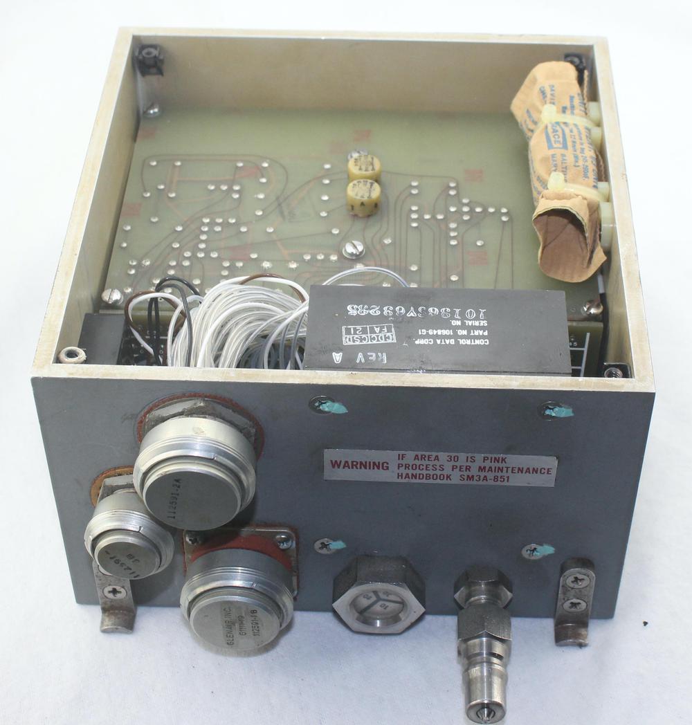
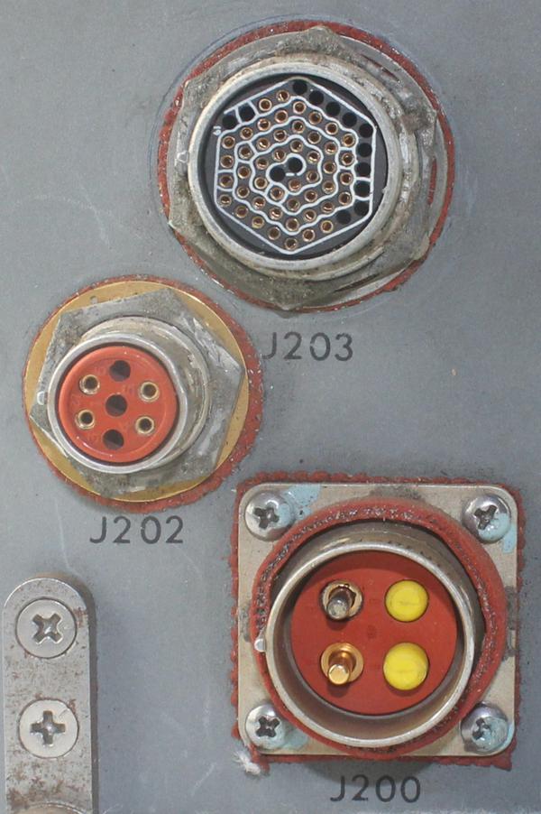
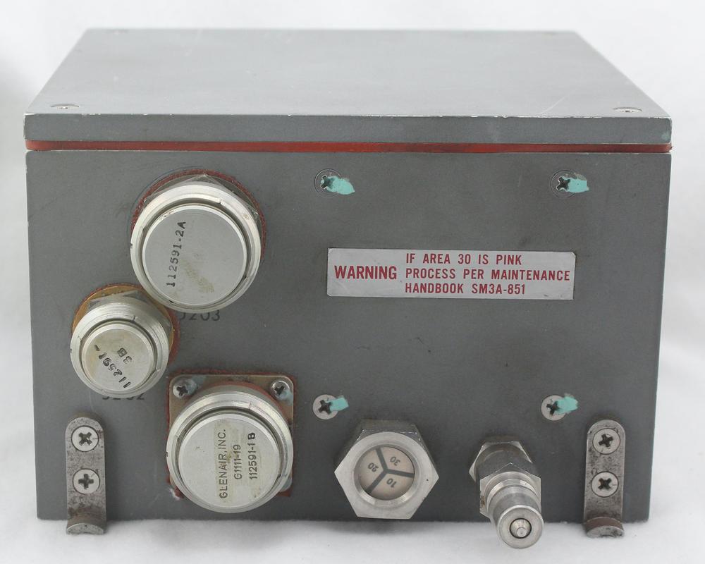
The Computer Buffer Unit is a 4"×6"×6" box. The three electrical connectors on the left are covered by protective covers. It has a humidity indicator and pressurization valve at the bottom.

The Computer Buffer Unit is a 4"×6"×6" box. The three electrical connectors on the left are covered by protective covers. It has a humidity indicator and pressurization valve at the bottom.

Testing for the Apollo missions

The Apollo spacecraft required extensive testing even while it was sitting on the launch pad. Thousands of different spacecraft components needed to be activated and analyzed for various tests. Since the control room was miles away from the launch pad, it wasn't practical to run separate wires to each component. Instead, NASA invented (and patented) a complex digital test system that communicated efficiently between the control room and the rocket. This test system sent digital commands to the launch site, where racks of control and interface units were wired to the spacecraft components. These units decoded the commands and performed the specified operation. Massive quantities of measurement data from the spacecraft were encoded digitally and serialized for communication back to the control room.

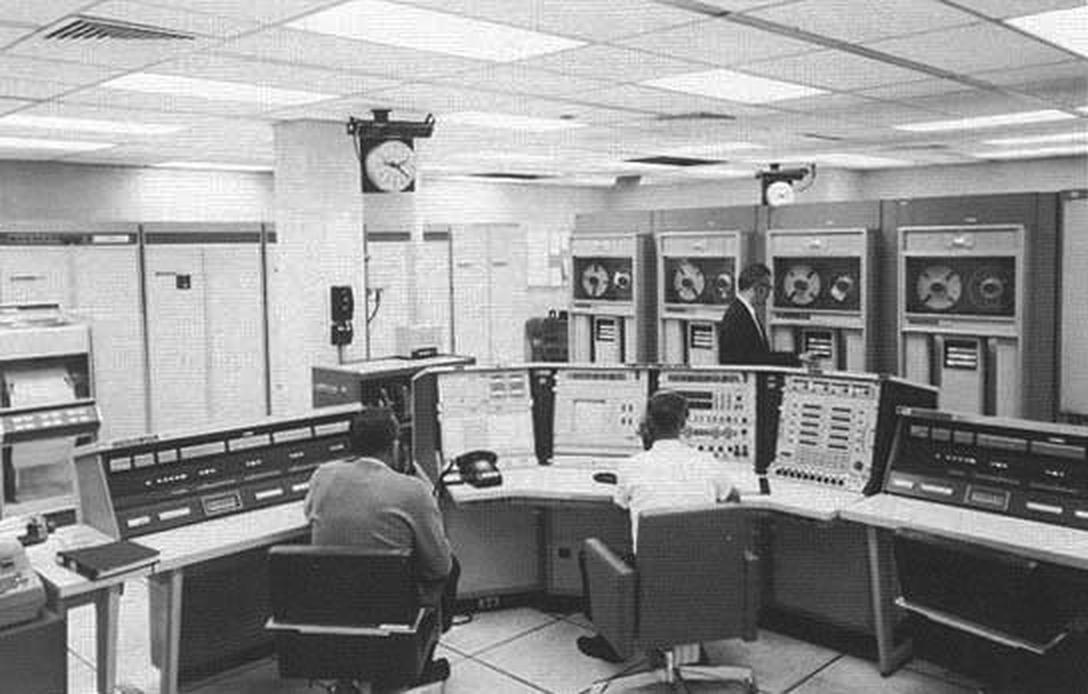
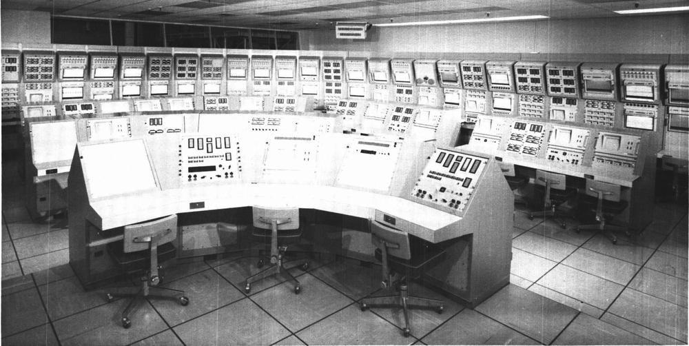
The complexity of testing is illustrated by the control room below.2 This is not Mission Control, but a separate control room specifically for testing, called ACE-S/C (Acceptance Checkout Equipment-Spacecraft). These consoles were crammed with control switches, tape readers, CRT displays, chart recorders, and status panels for conducting tests and recording results. The ACE-S/C system supported manual, semiautomatic, and automatic testing, driven by two minicomputers1.

ACE control room. From Applicability of Apollo Checkout Equipment.

All parts of the spacecraft were tested, including the fuel cells, cryogenic fuel storage, communications, and environmental control. For this blog post, the relevant subsystem is "Guidance and Navigation", responsible for determining the Apollo spacecraft's position in space using inertial navigation and guiding it on the proper trajectory including the landing on the Moon's surface. The key to Guidance and Navigation was the Apollo Guidance Computer, 70-pound computers onboard the Lunar Module and the Command Module.

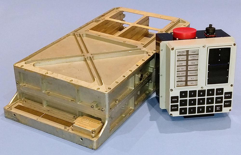
The Apollo Guidance Computer that we restored, next to a replica DSKY.

The Apollo Guidance Computer that we restored, next to a replica DSKY.

In space, astronauts operated the Apollo Guidance Computer through the Display/Keyboard (DSKY), a box (above) with keys, indicator lights, and numeric displays. But for ground testing, there needed to be a way to feed commands into the Apollo Guidance Computer from the testing system. The solution was the Computer Buffer Unit, the box that I'm examining. To operate the Apollo Guidance Computer remotely, the ACE test system encoded each DSKY keypress as a 16-bit command3 and sent it to the Buffer Unit. The Buffer Unit converted the message to serial, transferring one bit at a time to the Apollo Guidance Computer, which then processed the desired keypress.4 Thus, the Apollo Guidance Computer could be controlled remotely for testing, providing control over the Guidance and Navigation system, and the Computer Buffer Unit was the interface with the Apollo Guidance Computer.

Inside the Computer Buffer Unit

Next, I'll discuss the physical construction of the Computer Buffer Unit. Removing the lid reveals the components inside.5 The main circuitry consists of six horizontal circuit boards wired into a vertical backplane board; the top board is visible below. One unusual feature is the bag of desiccant inside the unit, zip-tied to the right side of the case. The designers of the unit were worried about Florida humidity and the risk of corrosion.6 To guard against damp air, the unit has a valve on the front so it can be pressurized with dry nitrogen. On the front of the unit, you can see a humidity sensor that changes color to indicate 10%, 20%, and 30% humidity. If the internal humidity exceeded 30%, the desiccant needed to be replaced, as described by the warning label.

The Buffer Unit with the lid removed.

The Buffer Unit with the lid removed.

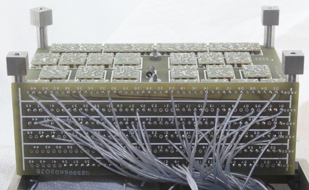
I removed the circuit boards with some difficulty, as they fit tightly. The photo below shows the stack of six printed circuit boards wired into the vertical backplane. The wires from the connectors are soldered directly to the backplane.

With the circuit boards pulled out of the unit, the wiring to the backplane is visible.

With the circuit boards pulled out of the unit, the wiring to the backplane is visible.

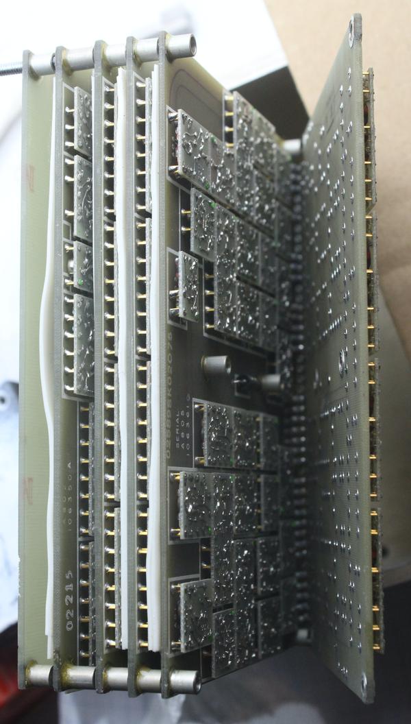
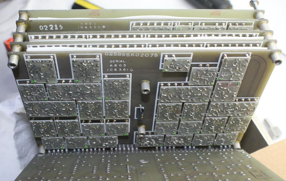
The circuit boards can be opened up like a book to provide access to the inner boards. The boards are not soldered directly to the backplane, but are connected by short, flexible wires, allowing them to swing apart. To prevent short circuits between the boards, they are separated by white sheets of (probably) silicone.

After removing six screws, the boards can be unfolded like a book.

After removing six screws, the boards can be unfolded like a book.

The circuitry is constructed in a very unusual way that I haven't seen before. Instead of mounting components directly on the circuit boards, components are mounted on small boards, each forming a module with a logic gate or two. These smaller modules are then soldered on pins above the main circuit boards, forming two-layer boards. Essentially they built pseudo-integrated-circuits on small boards, and then constructed the circuitry from these modules.

Closeup of logic modules mounted on the circuit board. A blue resistor is visible on the underside of the module.

Closeup of logic modules mounted on the circuit board. A blue resistor is visible on the underside of the module.

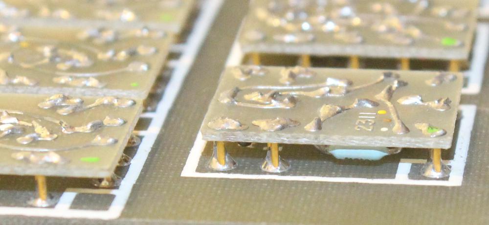
It is difficult to see the components sandwiched between the main board and the smaller modules, but the side view below shows some of the components. The two boards are connected by the vertical pins. A tiny glass diode is visible towards the left. The longer components are resistors. The shiny metal-can transistors are in the middle of the module and harder to see.

This side view shows a latch module (bottom) attached to the circuit board (top). The diodes, resistors, and transistors of the latch module are visible.

This side view shows a latch module (bottom) attached to the circuit board (top). The diodes, resistors, and transistors of the latch module are visible.

One question is why the circuitry is implemented with small circuit boards attached to the larger circuit board, instead of mounting the components directly on the circuit board. This approach seems overly complex and makes the boards twice as thick. One advantage, though, is that the separate logic modules could be manufactured, testing, and repaired separately, important in an era when semiconductors were less reliable. Second, the main boards and the logic modules are different types of printed circuit boards: four-layer circuit boards with widely-spaced traces versus single-sided but dense boards.

Logic gates

The circuitry is implemented with a logic family called Diode-Transistor Logic (DTL). This type of logic was used in the early 1960s as it only required one (expensive) transistor per gate, using cheaper diodes where possible. As transistor prices dropped, Transistor-Transistor Logic (TTL) became more popular because of its better performance. Nowadays fast, low-power CMOS logic is used in most integrated circuits.

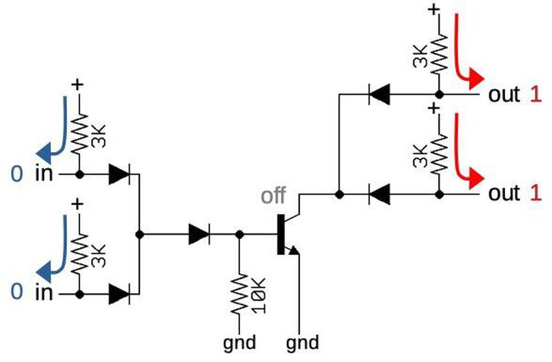
I reverse-engineered the schematic below, which shows a NOR gate from this unit. This gate has two inputs, as well as two outputs (for reasons that will be explained below). If both inputs are low (0), the transistor will be turned off. As a result, the resistors pull the outputs high, producing 1 outputs.

The NOR gate with both inputs low, outputs high.

The NOR gate with both inputs low, outputs high.

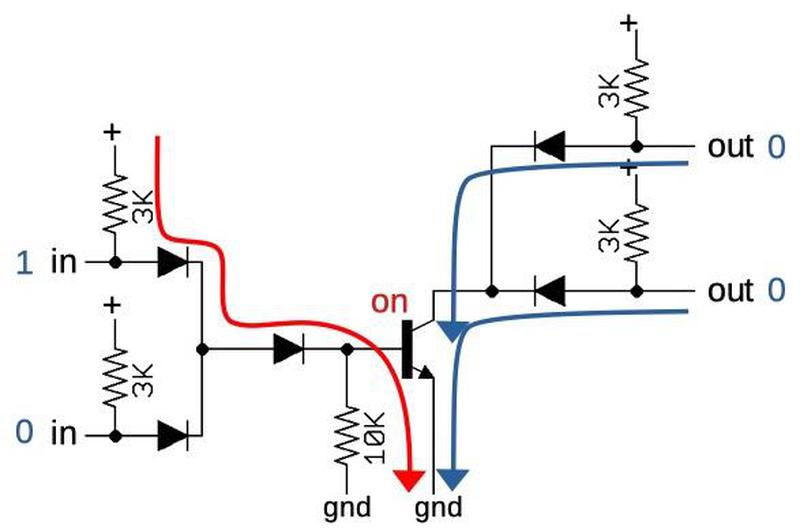
If an input is high, the circuit behaves as shown below. Current flows from the input pull-up resistor through the diodes and the transistor's base, turning the transistor on. As a result, current flows from the outputs, through the transistor to ground, pulling the outputs low. Thus, the circuit implements a NOR gate: the output is 1 if all inputs are low, and 0 otherwise.

The NOR gate with a high input, outputs high.

The NOR gate with a high input, outputs high.

The reason for multiple outputs is clever. If you connect the outputs from multiple gates together, this combined output will be pulled low if any output is low (i.e. the transistor is turned on), and otherwise will be pulled high by the resistor.7 This logic is equivalent to an AND gate. Note that the AND gate is implemented "for free" by wiring outputs together, without requiring additional logic; this is called wired-AND. However, you can't use a gate's output in two different wired-AND gates, since everything will be shorted together. Instead, a gate provides multiple outputs that can be wired independently; the diodes keep the outputs isolated from each other.

The board I examined has 5 different types of logic module8, from an inverter with 1 input and 8 outputs to a module with two 2-input, 5-output NOR gates. These modules follow the circuit above, but with different numbers of inputs and outputs.

Implementation of the shift register

The idea behind a shift register is to store multiple bits in a row. Each time a clock signal is activated, the bits are shifted by one position. Shift registers can be used to store data, convert parallel data to serial, or convert serial data to parallel. In this Buffer Unit, the shift register converted a 16-bit parallel value from the test equipment into a serial stream of bits for the Apollo Guidance Computer.9

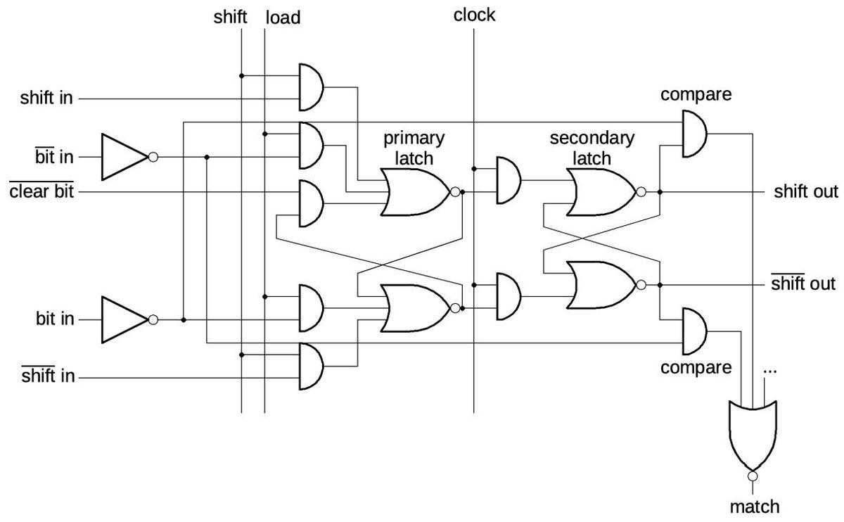
The board implements four bits of the 16-bit shift register. The schematic below shows the circuitry for a one-bit stage of the shift register. There's a lot going on, but I'll try to explain it. The heart of the stage consists of two latches, which store one bit. A bit is stored by first updating the primary latch, and then the secondary latch. (Each latch consists of two cross-coupled NOR gates, and can hold either a 0 or a 1.) The shift out lines are the outputs from the shift register stage, a regular output and an inverted output.

One stage of the shift register. It can read the bits in parallel, or shift a bit from one stage to the next.

One stage of the shift register. It can read the bits in parallel, or shift a bit from one stage to the next.

Each shift out line is fed to the shift in lines of the next stage, allowing the bits to be transferred from stage to stage through the shift register. The shift and load control lines, along with the AND gates, select the input to each stage. With shift high, the input will be the shift out from the previous stage. With load high, the input reads the external bit in lines. This allows a 16-bit data word to be read into the shift register in parallel. (I'm not sure what the clear bit function is used for.) After a bit has been loaded into the primary latch, the clock line is activated to load the bit into the secondary latch, completing the shift or load cycle.

An interesting function of the unit is that after loading, the value in the latch is compared to the input value, to make sure that the circuit is operating correctly. If there is a mismatch, a compare AND gate will activate, clearing the match line. (A compare AND gate will activate if the input bit is 1 and the latch bit is 0, or vice versa.) This circuit also detects a fault in the bit input wires. Each bit is provided over two wires: one with the bit value and one with the inverted bit value. If a wire is broken or affected by noise, the comparison will fail.10

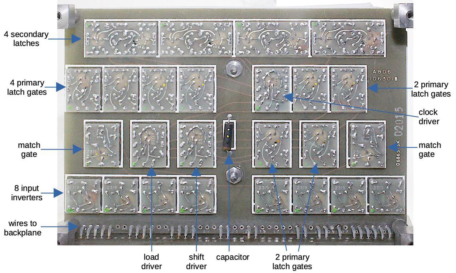
This diagram shows the functions of the gates. Note that the circular golden transistors are faintly visible through the circuit boards.

This diagram shows the functions of the gates. Note that the circular golden transistors are faintly visible through the circuit boards.

The board above11 contains four of these shift-register stages. The photo above shows how these stages map onto the hardware. The external signals (4 pairs of bit lines) enter at the bottom of the board, and pass through the input inverters. The 8 primary latch NOR gates implement four primary latches. Four secondary latch modules implement the four secondary latches, since each module contains two NOR gates. The clock driver, load driver, and shift driver provide 8 copies of the clock, load, and shift signals for the circuitry. Finally, the two match NOR gates combine the 8 match signals. (Note that since the AND gates are implemented with wired-AND, they don't use additional circuitry and do not appear in this diagram.)

I/O and power

I'll wrap up with a few comments on the I/O and power supply for the Buffer Unit. The unit has three military-style connectors on the front. At the top is a 61-pin connector for receiving the parallel data and control signals from ground equipment. (The pin count is larger than you might expect because each bit uses two wires as discussed earlier. Also, many of the 61 pins are unused.)

The unit has three connectors. The unit receives parallel data from ground equipment through the 61-pin connector at the top. The middle connector communicates the serial data to the Apollo Guidance Computer. The unit is powered with 28 volts through the bottom connector, which has larger pins for the high-current supply.

The unit has three connectors. The unit receives parallel data from ground equipment through the 61-pin connector at the top. The middle connector communicates the serial data to the Apollo Guidance Computer. The unit is powered with 28 volts through the bottom connector, which has larger pins for the high-current supply.

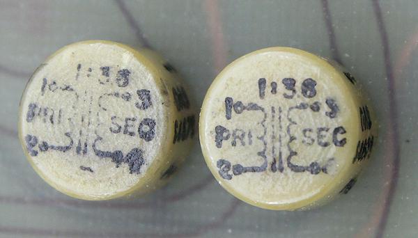
The middle connector has four pins that provide the serial data stream to the Apollo Guidance Computer. The wiring is a bit unusual. Instead of transmitting data over one serial line, the unit uses two pairs of lines: one to transmit "0" bits and one to transmit "1" bits. To provide electrical isolation between the unit and the Apollo Guidance Computer, these signals are transmitted via two small pulse transformers, shown below. When a pulse is fed into a pulse transformer, a similar pulse is produced on the output. (In modern equipment, an optoisolator provides similar functionality.)

Two pulse transformers on the top circuit board. Each small transformer is about 1 cm in diameter.

Two pulse transformers on the top circuit board. Each small transformer is about 1 cm in diameter.

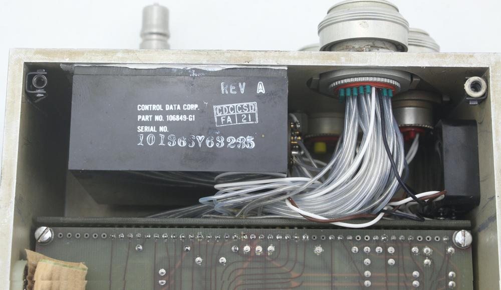
The bottom connector on the unit has two thick pins to provide 28 volts to the unit. This view inside the unit shows the power converter, a sealed black box. I believe this is a switching power supply module that converted the 28-volt input into the lower voltage required by the logic circuitry. It also provided electrical isolation from the power supply. The smaller black box on the right is an EMI filter on the power input; the Apollo ground test equipment encountered faults from voltage transients and electrical noise, so they added filtering.

The power supply components are sealed in black plastic.

The power supply components are sealed in black plastic.

Conclusion

This Computer Buffer Unit was built in 1965, a time when the industry was shifting from transistors to integrated circuits. This may explain the Unit's unusual construction technique, small circuit-board modules that are like integrated circuits built from discrete components.12 Interestingly, Motorola built a similar Buffer Unit for NASA that used integrated circuits (but was just as large),13 illustrating that transistors and integrated circuits were both viable approaches in 1965.

This box also illustrates the rapid pace of integrated circuit technology since the 1960s. The first commercial MOS integrated circuit was a 20-bit shift register introduced in 1964 and by 1970, Intel was producing a 512-bit shift register. In 1971, Western Digital was selling a UART chip, putting a complete parallel-to-serial and serial-to-parallel communication system onto a chip. Thus, it took 6 years to shrink the complex shift-register box down to a single chip (more or less). Nowadays, this functionality forms a tiny part of a complex chip. Coincidentally, Moore's Law, describing the exponential growth of integrated circuits, was published in 1965, the same year this box was manufactured.

I announce my latest blog posts on Twitter, so follow me @kenshirriff. (The Twitter thread corresponding to this blog post is here.) I also have an RSS feed. Thanks to Steve Jurvetson for letting me examine this artifact. A video tour of his space museum is here. Thanks to Mike Stewart for providing documents and extensive information on this box.

Notes and references

  1. The photo below shows the ACE computer room that supported ACE testing. The system was controlled by two 13-bit CDC 160-G minicomputers. Strangely, the CDC 160-G minicomputers were 13-bit computers, with 13-bit addresses, 13-bit registers, and 13-bit arithmetic. The earlier CDC 160 computer was 12 bits, and CDC improved the 160-G model by adding one more bit. The CDC 160 was designed by Seymour Cray, reportedly over a weekend.

    "An ACE Station with twin Control Data computers." From Computers in Spaceflight.

    "An ACE Station with twin Control Data computers." From Computers in Spaceflight.


  2. There were about 10 ACE installations for testing at various sites. ACE testing was performed at contractor sites, as well as at the launch pad. 

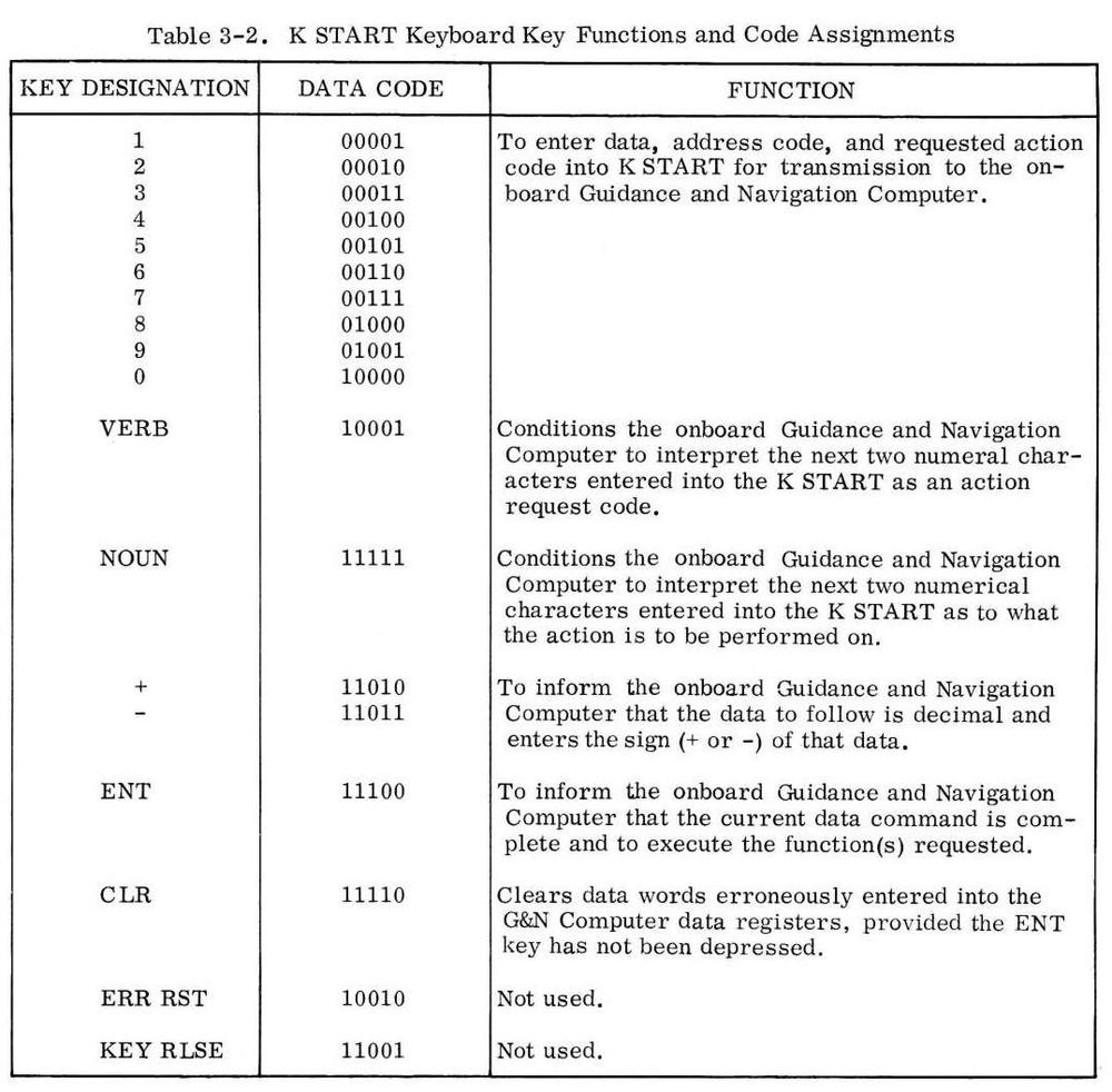
  3. To send a DSKY keypress through the testing system, each keypress was encoded as 5 bits as shown below. The 16-bit message consisted of a 1 bit followed by three copies of the 5-bit keypress, with the middle copy inverted. (Sending the keypress in triplicate detected communication errors.)

    The encoding of keys when communicating with the Apollo Guidance Computer. From ACE-S/C Operator's Manual.

    The encoding of keys when communicating with the Apollo Guidance Computer. From ACE-S/C Operator's Manual.


  4. The serial protocol used by the Apollo Guidance Computer is a bit unusual compared to modern serial protocols. Instead of a single serial line, it used two pairs of wires: one to receive a 1 bit and one to receive a 0 bit. This worked well with the Apollo Guidance Computer hardware, which included a feature for incrementing and decrementing counters in response to interrupts. In particular, a serial input 0 triggers a SHINC instruction (shift left), while a serial input 1 triggers a SHANC (shift and increment by 1) instruction.

    (The interrupt-triggered counter mechanism worked well except during the Apollo 11 landing, when the power supply for the Apollo Guidance Computer and the power supply for the rendezvous radar had a phase difference. For complex reasons, this resulted in a high rate of interrupts, overloading the Apollo Guidance Computer and causing restarts. This was indicated by the famous 1201 and 1202 program alarms during the landing.)

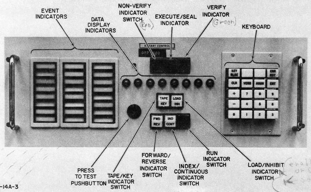
    The K-START (Keyboard - Selections To Actuate Random Testing) panel is used to send commands to the Apollo Guidance Computer. From ACE-S/C Operator's Manual.

    The K-START (Keyboard - Selections To Actuate Random Testing) panel is used to send commands to the Apollo Guidance Computer. From ACE-S/C Operator's Manual.

    In the ACE testing control room, DSKY keypresses were entered on a panel called K-START (Keyboard - Selections To Actuate Random Testing), shown above. The keyboard corresponds to the keyboard on the DSKY, while it has other switches specific to testing. These key entries could also be recorded on perforated tape and played back at high speed. 

  5. Another interesting feature of the unit is how it is mounted on a rack. The back of the unit has two Teflon-lined holes. Two "dagger pins" from the rack fit into these holes. On the front, the unit has two small hold-down hooks; a knob on the rack engages with the hook to hold the unit in place. The mounting hooks are type NAS 622, an aerospace standard. The hold-down mechanism is described here.

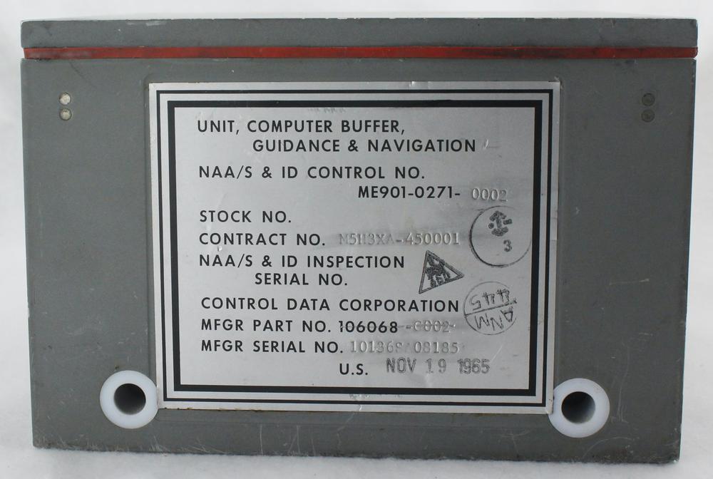
    Back of the Buffer Unit with identifying label and two holes for dagger pins. The labels say "Unit, Computer Buffer Guidance & Navigation. NAA/S & ID Control No. ME901-0271-0002. Stock No. Contract No. M5H3XA-450001. NAA/S & ID Inspection Serial No. Control Data Corporation MFGR Part No. 106068-0002. Mfgr Serial No. 10136SA08185. US Nov 19 1965.

    Back of the Buffer Unit with identifying label and two holes for dagger pins. The labels say "Unit, Computer Buffer Guidance & Navigation. NAA/S & ID Control No. ME901-0271-0002. Stock No. Contract No. M5H3XA-450001. NAA/S & ID Inspection Serial No. Control Data Corporation MFGR Part No. 106068-0002. Mfgr Serial No. 10136SA08185. US Nov 19 1965.


  6. The document Acceptance Checkout Equipment for the Apollo Spacecraft discusses the corrosion problems encountered by the test equipment due to humidity and insufficient air conditioning. The specifications don't discuss pressurization of the unit, but I'm assuming they used nitrogen based on other items I've studied. 

  7. One subtlety with the wired-AND gate is that connecting multiple outputs together will result in multiple pull-up resistors in parallel, which may provide too much pull-up current. The solution is that some gates have outputs without pull-up resistors, so each wired-AND output has a single pull-up. The wired-AND isn't entirely free, since the multiple outputs require multiple diodes, but diodes are inexpensive compared to transistors. I should admit that I'm not 100% sure of the circuitry. Since the components are all hidden underneath the module, I had to deduce the circuitry by probing it from above. There were a few inputs that didn't seem to have connectivity; perhaps there are capacitors to make these inputs pulse-based. 

  8. The board I examined uses the following types of modules:
    2304: 1-in, 8-out inverter
    2309: 3-in, 4 out NOR
    2311: 4-in, 2-out NOR
    2319: 1-in, 4-out inverter
    2314: dual 2-in, 5-out NOR (larger than the other modules) 

  9. The specifications for the Buffer Unit describe its purpose: "This specification covers the requirements for a Guidance and Navigation Computer Buffer Unit, hereinafter referred to as the G&N buffer. The G&N buffer shall form a part of the Digital Test Command System (DTCS) which is the up-link portion of the Automatic Checkout Equipment (ACE). The ACE will be used as ground support equipment for the Apollo space craft. The G&N buffer shall receive remotely generated digital test commands from the control room via the DTCS and shall store, verify, and shift out G&N data in appropriate format to the G&N on-board computer."

    Functional diagram of the Buffer Unit. Image from Specification MC 901-0666 courtesy of Mike Stewart.

    Functional diagram of the Buffer Unit. Image from Specification MC 901-0666 courtesy of Mike Stewart.

    The specifications for the Computer Buffer Unit can be viewed online: MC901-0666, ME901-0666, ME901-0271, ME476-0070.

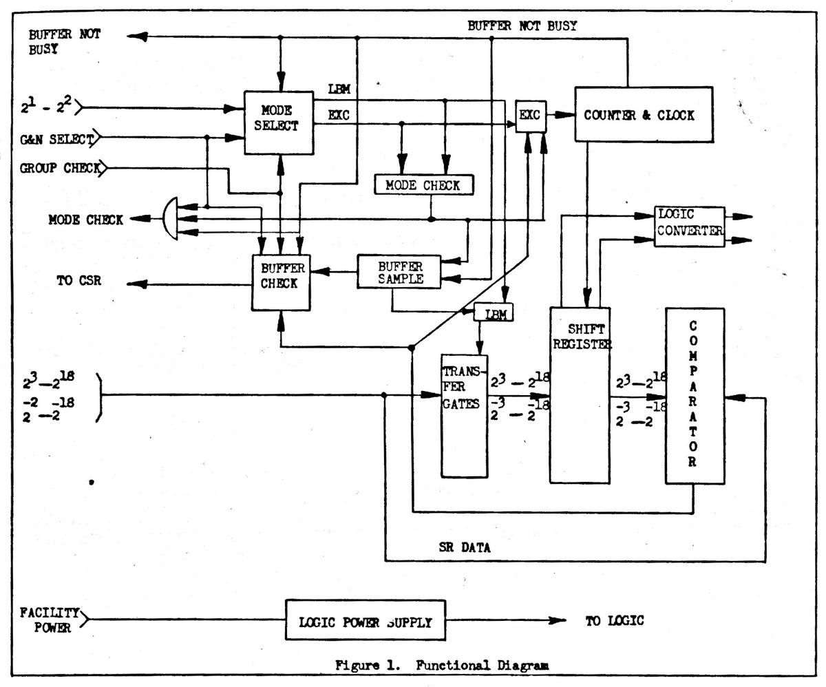
    The unit includes more functionality than just a shift register (but not much more). As shown in the functional diagram above, the unit also includes the clock oscillator that controls the timing of the serial pulses. Second, it contains a control circuit to handle loading the bits in parallel and then shifting them out serially. Third, for reliability reasons, it has a comparator circuit to check that the bits loaded into the shift register match the input bits. 

  10. Modern systems often use differential signaling, using two complementary signals for a bit. Looking at the difference between the two signals provides noise immunity, since electrical noise will often affect both signals equally, and thus will be canceled out. Although the Buffer Unit uses two complementary signals, it doesn't provide this noise immunity, since the two signals are processed independently rather than differentially. 

  11. I only reverse-engineered one of the boards, since I didn't want to risk more disassembly, and one board is enough to understand the basic logic. I studied board 6 of the unit, which implements bits 15 through 18 of the shift register. Board 3 implements bits 3-6, board 4 implements bits 7-10, as well as mode bits 1 and 2, board 5 implements bits 11 through 14, and board 6 (the one I examined) implements bits 15 through 18. Boards 2 and 4 implement control logic, while board 1 has the output driver transformers.

    With board 6 folded down, board 5 is visible.

    With board 6 folded down, board 5 is visible.

    The photo above shows board 5. Note that the circuit layout is entirely different from board 6. I thought that the unit might consist of four identical 4-bit shift register boards, but it turns out that the boards are optimized for particular roles. 

  12. In the context of "not-quite-integrated circuits", I should mention IBM's use of hybrid modules (called SLT) for the System/360 mainframes. These small aluminum-cased modules contained a few transistor or diodes as silicon dies, mounted on a ceramic substrate along with thick-film resistors. These modules were not quite integrated circuits, since they were built from discrete (but unpackaged) components. But they were closer to integrated circuits than the modules in the Buffer Unit, which used packaged transistors, resistors, and diodes on a printed circuit board. 

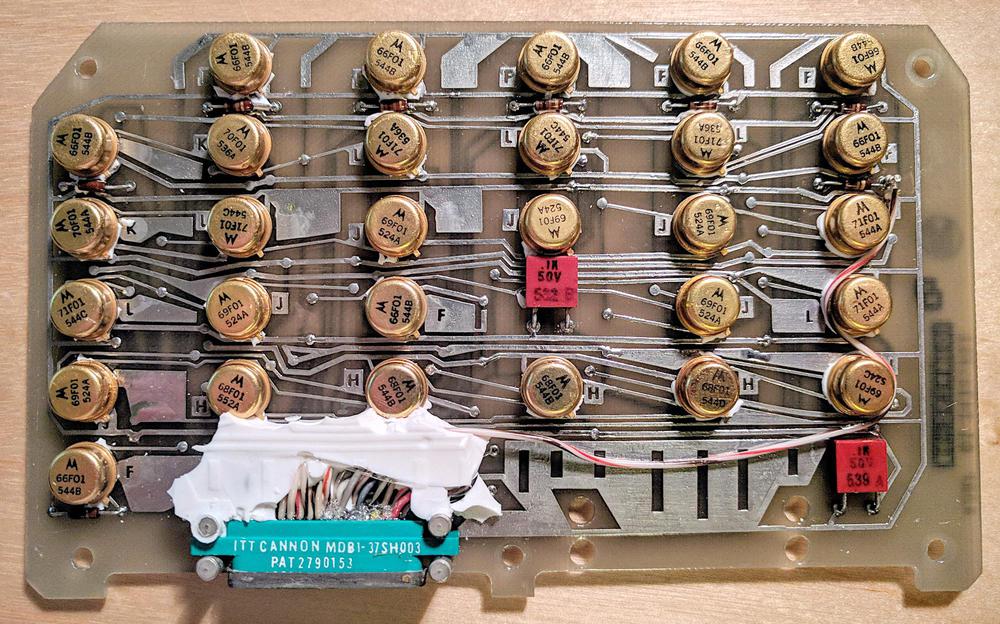
  13. Motorola made a similar Buffer Unit, but they used integrated circuits, specifically Motorola's line of high-speed ECL chips, introduced in 1962. Since each chip is a few gates, it still took multiple boards to build the unit. Apollo Guidance Computer expert Mike Stewart has photos of the Motorola box here, as well as reverse-engineered schematics. The functionality of the Motorola box is nearly identical, except it has separate inputs for the 16-bit compare value. It is built with chips such as the MC308 flip flop and MC 309 dual NOR gate, described here.

    A board from the Motorola version of the Buffer Unit. Each metal can is an integrated circuit. Photo courtesy of Mike Stewart.
    A board from the Motorola version of the Buffer Unit. Each metal can is an integrated circuit. Photo courtesy of Mike Stewart.
     

Teardown of a PC power supply

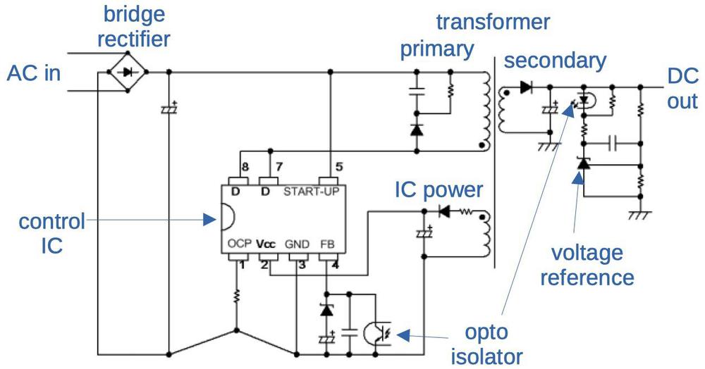
Have you ever wondered what's inside your computer's power supply? The task of a PC power supply is to convert the power from the wall (120 or 240 volts AC) into stable power at the DC voltages that the computer requires. The power supply must be compact and low-cost while transforming the power efficiently and safely. To achieve these goals, power supplies use a variety of techniques and are more complex inside than you might expect. In this blog post, I tear down a PC power supply and explain how it works.1
The power supply I examined, like most modern power supplies uses a design known as a "switching power supply." Switching power supplies are now very cheap, but this wasn't always the case. In the 1950s, switching power supplies were complex and expensive, used in aerospace and satellite applications that needed small, lightweight power supplies. By the early 1970s, though, new high-voltage transistors and other technology improvements made switching power supplies much cheaper and they became widely used in computers. Now, you can buy a phone charger for a few dollars that contains a switching power supply.
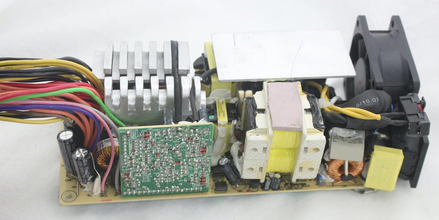
The ATX power supply that I examined was packaged in a metal box the size of a brick, with a remarkable number of colorful cables emerging from it. Removing the case reveals the components below, tightly packed to keep the power supply compact. Many of the components are hidden by the heat sinks that keep the power semiconductors cool along with the fan at the right.

The power supply, removed from the case. The large bundle of wires at the left is connected to the computer.  The large component in the middle that looks like a transformer is a filter inductor. Click this photo (or any other) for a larger version.

The power supply, removed from the case. The large bundle of wires at the left is connected to the computer. The large component in the middle that looks like a transformer is a filter inductor. Click this photo (or any other) for a larger version.

I'll start with a quick overview of how the switching power supply works, and then describe the components in detail. Starting at the right, the power supply receives AC power. The input AC is converted to high-voltage DC, with the help of some large filtering components. This DC is switched on and off thousands of times a second to produce pulses that are fed into a transformer, which converts the high-voltage pulses into low-voltage, high-current pulses. These pulses are converted to DC and filtered to provide nice, clean power, which is fed to the computer's motherboard and disk drives through the bundle of wires on the left.

While this process may seem excessively complex, most consumer electronics, from your cell phone to your television, use a switching power supply. The high frequencies allow the use of a small, lightweight transformer. In addition, switching power supplies are very efficient; the pulses are adjusted to supply just the power needed, rather than turning excess power into waste heat as in a "linear" power supply.

Input filtering

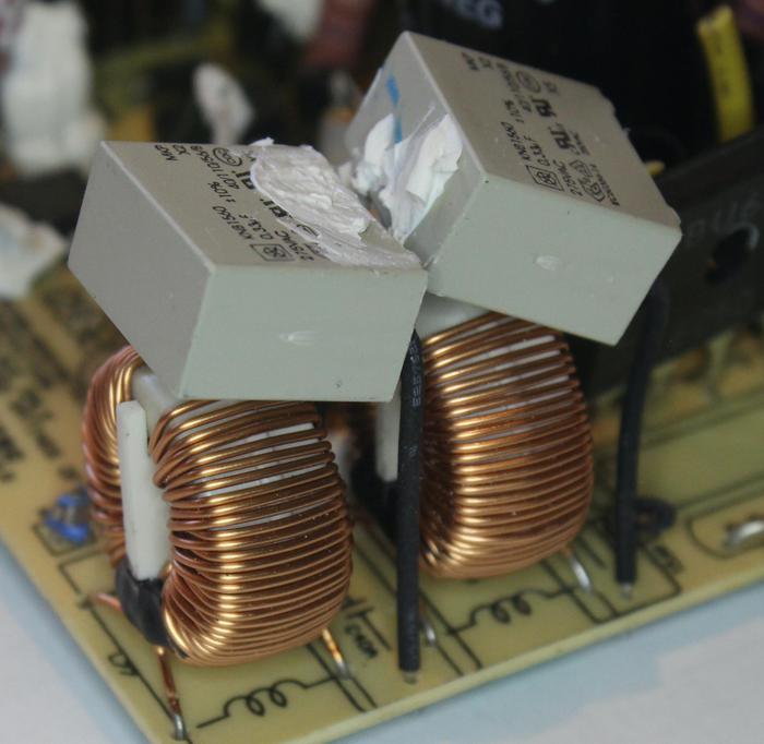
The first step is for the input AC to go through an input filter circuit that blocks electrical noise from exiting the power supply. The filter below consists of inductors (the toroidal coils) and capacitors. These boxy gray capacitors are special Class-X capacitors, designed to be connected safely across the AC lines.

The input filter components

The input filter components

Rectification: converting AC to DC

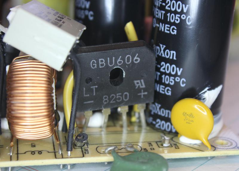
The 60-Hertz AC (alternating current) from the wall oscillates 60 times a second, but the power supply needs steady DC (direct current) that flows in one direction. The full-bridge rectifier below converts the AC to DC. The rectifier below is marked with "-" and "+" for the DC outputs, while the two center pins are the AC input. Internally the rectifier contains four diodes. A diode allows current to pass in one direction and blocks it in the other direction, so the result is that the alternating current is converted to direct current, flowing in the desired direction.

The bridge rectifier is labeled "GBU606". Filter circuitry is to its left. To the right, the large black cylinder is one of the voltage-doubler capacitors.
The small yellow capacitor is a special Y capacitor, designed for safety.

The bridge rectifier is labeled "GBU606". Filter circuitry is to its left. To the right, the large black cylinder is one of the voltage-doubler capacitors. The small yellow capacitor is a special Y capacitor, designed for safety.

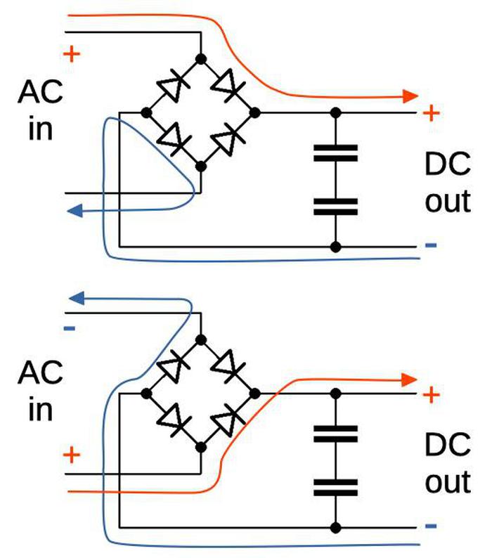
The diagram below shows how the bridge rectifier works. In the first schematic, the AC input has the upper side positive. The diodes pass the voltage through to the DC output. In the second schematic, the AC input has reversed direction. However, the configuration of the diodes ensures that the DC output voltage stays the same (positive on top). The capacitors smooth out the output.

The two schematics show the flow of current as the AC input oscillates. The diodes force current to flow in the direction indicated by their arrow shape.

The two schematics show the flow of current as the AC input oscillates. The diodes force current to flow in the direction indicated by their arrow shape.

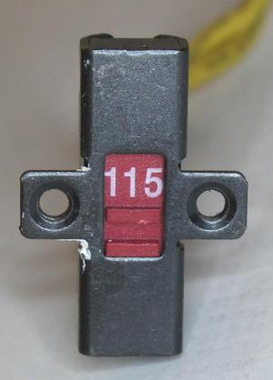
Modern power supplies accept a "universal" input voltage of 85 to 264 volts AC, so they are usable in different countries regardless of the country's voltage. However, the circuitry of this older power supply couldn't handle such a wide input range. Instead, you had to flip a switch (below) to select between 115 V and 230 V.

The 115/230 V switch.

The 115/230 V switch.

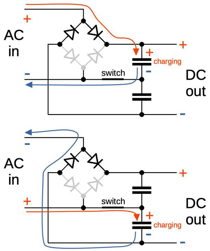
The voltage selection switch used a clever circuit, a voltage doubler. The idea is that with the switch closed (for 115 volts), the AC input bypasses the bottom two diodes in the bridge rectifier and is instead connected directly to the two capacitors. When the AC input is positive on top, the top capacitor is charged with the full voltage. And when the AC input is positive on the bottom, the lower capacitor is charged with the full voltage. Since the DC output is across both capacitors, the DC output has double the voltage. The point of this is that the rest of the power supply receives the same voltage, whether the input is 115 volts or 230 volts, simplifying its design. The downsides of the voltage doubler are that the user must put the switch in the correct position (or risk destroying the power supply), and the power supply requires two large capacitors. For these reasons, the voltage doubler has gone out of style in more recent power supplies.

The voltage doubler circuit. Each capacitor is charged with the full voltage, so the DC output has double the voltage. The grayed-out diodes are not used when the doubler is active.

The voltage doubler circuit. Each capacitor is charged with the full voltage, so the DC output has double the voltage. The grayed-out diodes are not used when the doubler is active.

Primary and secondary

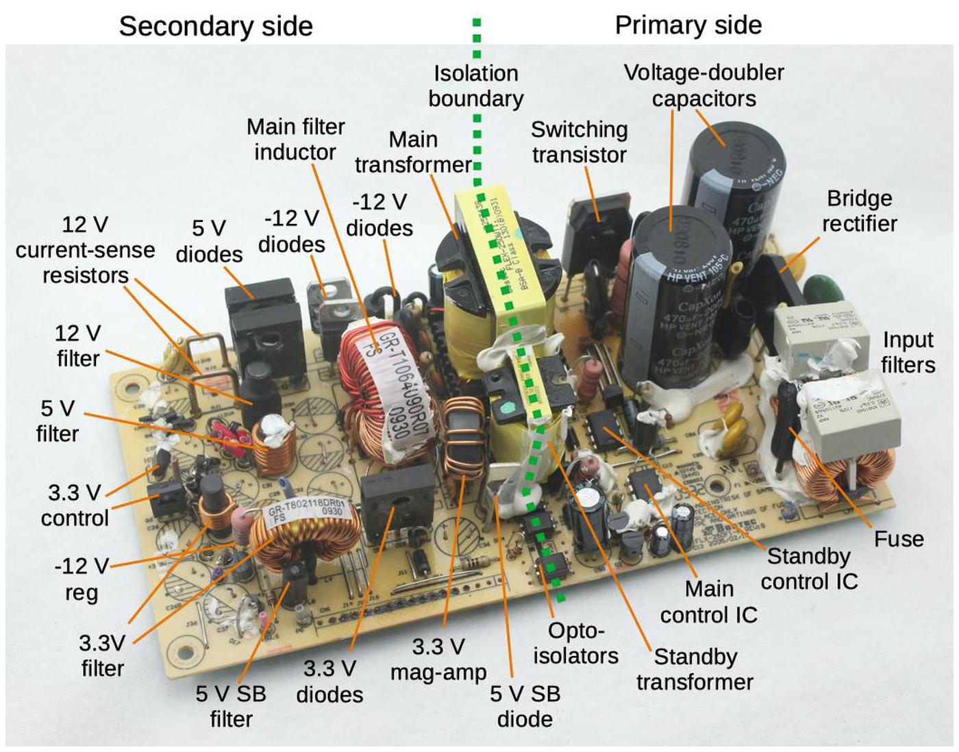
For safety, the high-voltage components and the low-voltage components are separated, both mechanically and electrically. The primary side below contains all the circuitry that is connected to the AC line. The secondary side contains the low-voltage circuitry. The primary and secondary are separated by an "isolation boundary" (shown in green), with no electrical connections across the boundary. The transformers pass power across this boundary through magnetic fields, without a direct electrical connection. Feedback signals are sent from the secondary to the primary by opto-isolators, which transmit signals optically. This separation is a key factor in safe power supply design: a direct electrical connection between the AC line and the output would create a high danger of electric shock.

The power supply with main features labeled. The heat sinks, capacitors, control board, and output wires have been removed to give a better view. (SB indicates the standby supply.)

The power supply with main features labeled. The heat sinks, capacitors, control board, and output wires have been removed to give a better view. (SB indicates the standby supply.)

Pulses to the transformer

At this point, the input AC has been converted to high-voltage DC, about 320 volts.2 The DC is chopped into pulses by the switching transistor above, a power MOSFET.3 Because this transistor gets hot during use, it was mounted on a large heat sink. These pulses are fed into the main transformer above, which in a sense is the heart of the power supply.

The transformer consists of multiple coils of wire wound around a magnetizable core. The high-voltage pulses into the transformer's primary winding produce a magnetic field. The core directs this magnetic field to the other, secondary windings, producing voltages in these windings. This is how the power supply safely produces its output voltages: there is no electrical connection between the two sides of the transformer, just a connection by the magnetic field. The other important aspect of the transformer is that the primary winding has the wire wrapped around the core a large number of times, while the secondary windings are wrapped around a much smaller number of times. The result is a step-down transformer: the output voltage is much smaller than the input, but at a much higher current.

The switching transistor3 is controlled by an integrated circuit, a "UC3842B current mode PWM controller". This chip can be considered the brains of the power supply. It generates pulses at the high frequency of 250 kilohertz. The width of each pulse is adjusted to provide the necessary output voltage: if the voltage starts to drop, the chip produces wider pulses to pass more power through the transformer.4

The secondary side

Now we can look at the secondary side of the power supply, which receives the low-voltage outputs from the transformer. The secondary circuitry produces the four output voltages: 5 volts, 12 volts, -12 volts, and 3.3 volts. Each output voltage has a separate transformer winding and a separate circuit to produce that voltage. Power diodes (below) convert the outputs from the transformer to DC, and then inductors and capacitors filter the output to keep it smooth. The power supply must regulate the output voltages to keep them at the proper level even as the load increases or decreases. Interestingly, the power supply uses several different regulation techniques.

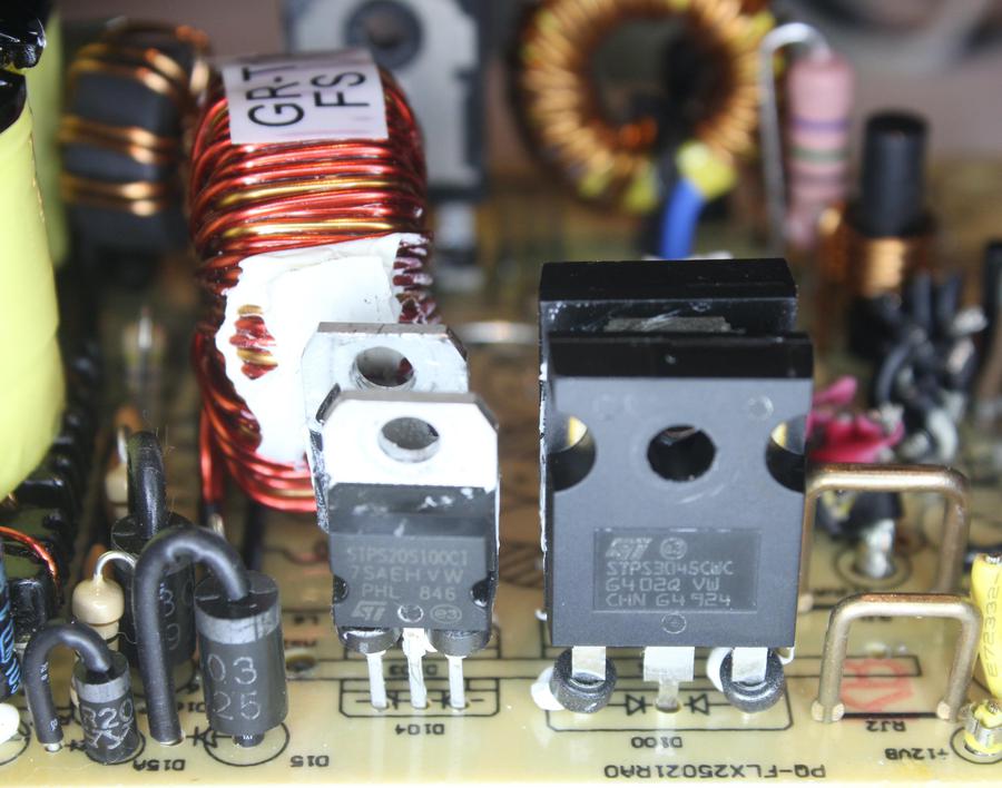
Closeup of the output diodes. At the left are cylindrical diodes mounted vertically. In the middle are pairs of rectangular power Schottky diodes; each package holds two diodes. These diodes were attached to a heat sink for cooling. At right note the two staple-shaped copper wires used as current-sensing resistors.

Closeup of the output diodes. At the left are cylindrical diodes mounted vertically. In the middle are pairs of rectangular power Schottky diodes; each package holds two diodes. These diodes were attached to a heat sink for cooling. At right note the two staple-shaped copper wires used as current-sensing resistors.

The main outputs are the 5-volt and 12-volt outputs. These are regulated together by the controller chip on the primary side. If the voltage is too low, the controller chip increases the width of the pulses, passing more power through the transformer and causing the voltage on the secondary side to increase. And if the voltage is too high, the chip decreases the pulse width. (The same feedback circuit controls both the 5-volt and 12-volt output, so the load on one output can affect the voltage on the other. Better power supplies regulate the two outputs separately.5)

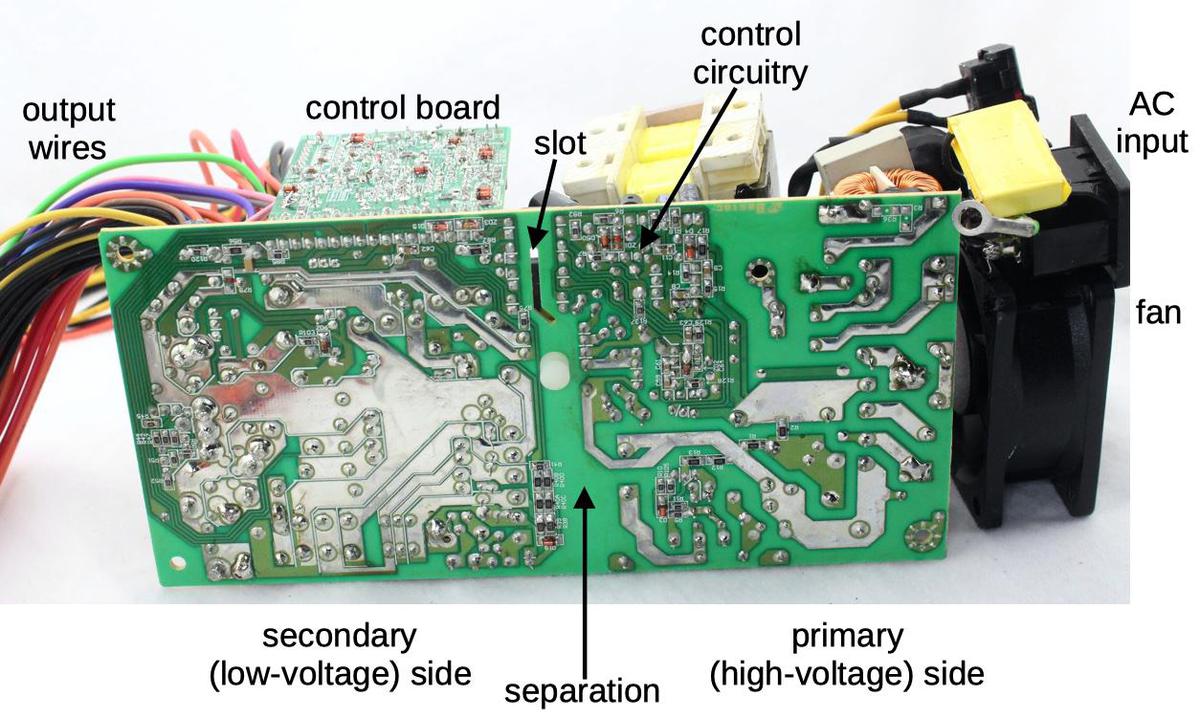
Underside of the power supply, showing the printed circuit board traces. Note that wide separation between the secondary-side traces on the left and
the primary-side traces on the right. Also note the wide metal traces used for the high-current supply and the thin traces for control circuitry.

Underside of the power supply, showing the printed circuit board traces. Note that wide separation between the secondary-side traces on the left and the primary-side traces on the right. Also note the wide metal traces used for the high-current supply and the thin traces for control circuitry.

You might wonder how the controller chip on the primary side receives feedback about the voltage levels on the secondary side, since there is no electrical connection between the two sides. (In the photo above, you can see the wide gap separating the two sides.) The trick is a clever chip called the opto-isolator. Internally, one side of the chip contains an infra-red LED. The other side of the chip contains a light-sensitive photo-transistor. The feedback signal on the secondary side is sent into the LED, and the signal is detected by the photo-transistor on the primary side. Thus, the opto-isolator provides a bridge between the secondary side and the primary side, communicating by light instead of electricity.6

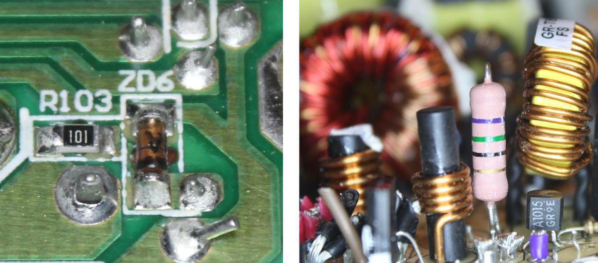
The power supply also provides a negative voltage output (-12 V). This voltage is mostly obsolete, but was used to power serial ports and PCI slots. Regulation of the -12 V supply is completely different from the 5-volt and 12-volt regulation. The -12V output is controlled by a Zener diode, a special type of diode that blocks reverse voltage until a particular voltage is reached, and then starts conducting. The excess voltage is dissipated as heat through a power resistor (pink), controlled by a transistor and the Zener diode. (Since this approach wastes energy, modern high-efficiency power supplies don't use this regulation technique.)

The -12 V supply is regulated by a tiny Zener diode "ZD6", about 3.6 mm long, on the underside of the circuit board. The associated power resistor and transistor "A1015" are on the top side of the board.

The -12 V supply is regulated by a tiny Zener diode "ZD6", about 3.6 mm long, on the underside of the circuit board. The associated power resistor and transistor "A1015" are on the top side of the board.

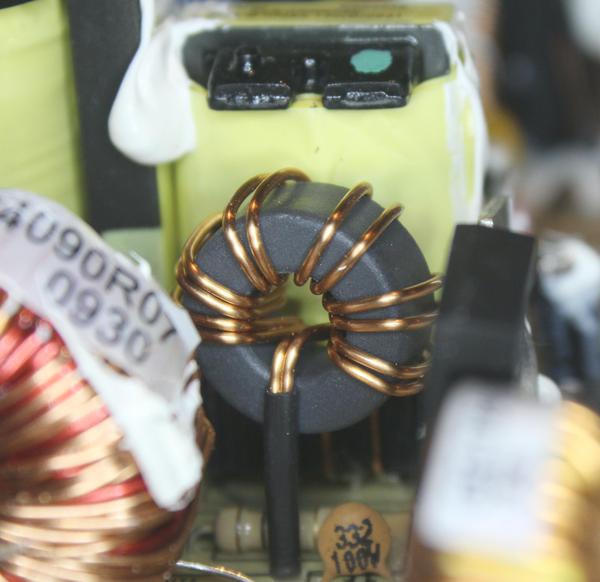
Perhaps the most interesting regulation circuit is for the 3.3-volt output, which is regulated by a magnetic amplifier. A magnetic amplifier is an inductor with special magnetic properties that make it behave like a switch. When a current is fed into the magnetic amplifier inductor, at first the inductor will almost completely block the current as the inductor magnetizes and the magnetic field increases. When the inductor reaches its full magnetization (i.e. it saturates), the behavior suddenly changes and the inductor lets the current flow unimpeded. In the power supply, the magnetic amplifier receives pulses from the transformer. The inductor blocks a variable part of the pulse; by changing the pulse width, the 3.3-volt output is regulated.7

The magnetic amplifier is a ring constructed from ferrite material with special magnetic properties. The ring has a few turns of wire wound around it.

The magnetic amplifier is a ring constructed from ferrite material with special magnetic properties. The ring has a few turns of wire wound around it.

The control board

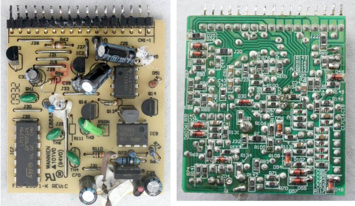
The power supply has a small board holding the control circuitry. This board compares the voltages against a reference to generate the feedback signals. It also monitors the voltages to generate a "power good" signal.8 This circuitry is mounted on a separate, perpendicular board so it doesn't take up much room in the power supply.

The control board has through-hole components on top and the underside is covered with tiny surface-mount components. Note the "zero-ohm" resistors marked with 0, used as jumpers.

The control board has through-hole components on top and the underside is covered with tiny surface-mount components. Note the "zero-ohm" resistors marked with 0, used as jumpers.

The standby power supply

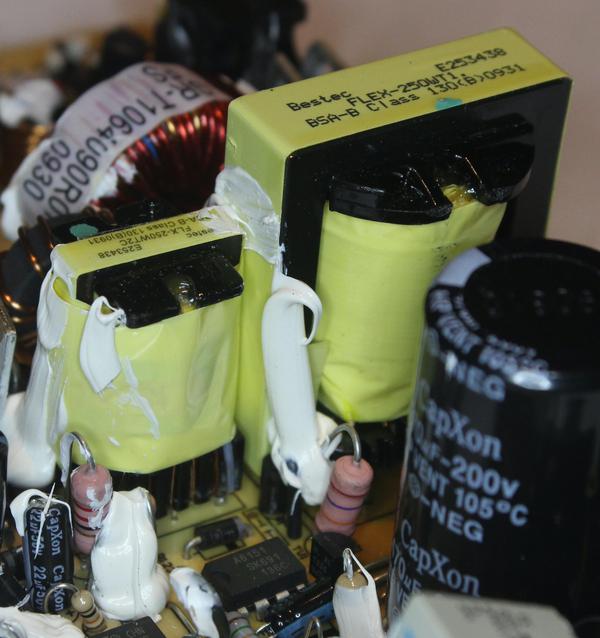
The power supply contains a second circuit for standby power.9 Even when the computer is supposedly turned off, the 5V standby supply is providing 10 watts. This power is used for features that need to be powered when the computer is "off", such as the real-time clock, the power button, and powering-on via the network ("Wake on LAN"). The standby power circuit is almost a second independent power supply: it uses a separate control IC, separate transformer, and components on the secondary side, although it uses the same AC-to-DC circuitry on the primary side. The standby power circuit provides much less power than the main circuit, so it can use a smaller transformer.

The black and yellow transformers: the transformer for standby power is on the left and the main transformer is on the right. The control IC for standby power is in front of the transformer. The large cylindrical capacitor on the right is part of the voltage doubler. The white blobs are silicone to insulate components and hold them in place.

The black and yellow transformers: the transformer for standby power is on the left and the main transformer is on the right. The control IC for standby power is in front of the transformer. The large cylindrical capacitor on the right is part of the voltage doubler. The white blobs are silicone to insulate components and hold them in place.

Conclusion

An ATX power supply is complex internally, with a multitude of components ranging from chunky inductors and capacitors to tiny surface-mount devices.10 This complexity, however, results in power supplies that are efficient, lightweight, and safe. In comparison, I wrote about a power supply from the 1940s that produced just 85 Watts DC, but was suitcase-sized and weighed over 100 pounds. Now, with advanced semiconductors, you can hold a much more powerful power supply for under $50 that you can hold in your hand.

I've written about power supplies before, including a history of power supplies in IEEE Spectrum. You might also like my Macbook charger teardown and iPhone charger teardown. I announce my latest blog posts on Twitter, so follow me at kenshirriff. I also have an RSS feed.

Notes and references

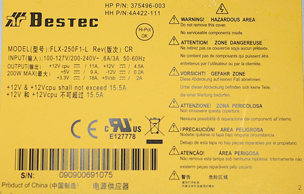
  1. Intel introduced the ATX standard for personal computers in 1995. The ATX standard (with some updates) still defines the motherboard, enclosure, and power supply configuration for most PCs. The power supply I examined is from 2005, so newer power supplies are more advanced and more efficient. The basic principles are the same, but there are some changes. For instance, regulation using DC-to-DC converters has mostly replaced the magnetic amplifier.

    The label on the power supply.

    The label on the power supply.

    The label provides information about the power supply I examined. It was built by Bestec for Hewlett-Packard's Dx5150 desktop PC. This power supply doesn't fit the ATX dimensions; it is longer and more rectangular. 

  2. You might wonder why an AC input of 230 volts yields 320 volts DC. The reason is that AC voltage is normally measured as root-mean-square which (sort of) averages the varying waveform. As a result, a 230-volt AC signal has peaks of 320 volts. The power supply capacitors charge through the diodes to the peak voltage, so the DC will be approximately 320 volts (although it will sag somewhat through the cycle). 

  3. The power transistor is an FQA9N90C power MOSFET. It can handle 9 amps and 900 volts. 

  4. The integrated circuit is powered by a separate winding on the transformer that provides 34 volts to run the chip. You might notice a chicken-and-egg problem: the control IC creates the pulses to the transformer, but the transformer powers the control IC. The solution is a startup circuit consisting of a 100 kΩ resistor between the IC and the high-voltage DC. This provides a small current, sufficient to start operation of the IC. Once the IC starts sending pulses to the transformer, it is powered by the transformer. 

  5. The technique of using one regulation loop for two outputs is called cross-regulation. If the load on one output is much higher than the load on the other, the voltages may diverge from their proper values. For this reason, many power supplies have a minimum load requirement on each output. More advanced power supplies use DC-to-DC converters for all the outputs to make sure they are precise. For more about cross-regulation, see this presentation and this presentation. One technique discussed is DC-stacking the output windings, a technique used in this power supply. Specifically, the 12-volt output is implemented as a 7-volt output "stacked" on top of the 5-volt output, yielding 12-volts. With this configuration, a 10% error (for example) in the 12-volt circuit would be just 0.7 V rather than 1.2 V. 

  6. The opto-isolators are PC817 components, which provide 5000 volts of isolation between the two sides. Note the slot cut in the circuit board underneath the opto-isolators. This provides additional safety, ensuring that dangerous voltages cannot pass between the two sides of the opto-isolator along the surface of the circuit board, for example if there were contamination or condensation on the board. (Specifically, the slot increases the creepage distance.) 

  7. The pulse width through the magnetic amplifier is set by a simple control circuit. During the reverse part of each pulse, the inductor is partially demagnetized. A control circuit adjusts the demagnetization voltage. A higher demagnetization voltage produces more demagnetization. This causes the inductor to take longer to re-magnetize and thus it blocks the input pulse for a longer time. With a shorter pulse passing through the circuit, the output voltage is decreased. Conversely, a lower demagnetization voltage produces less demagnetization, so the input pulse is blocked for a shorter time. Thus, the output voltage is regulated by changing the demagnetization voltage. Note that the pulse width into the magnetic amplifier is controlled by the control IC; the magnetic amplifier cuts these pulses shorter as needed to regulate the 3.3 V output. 

  8. The control board contains multiple ICs including an LM358NA op-amp, a TPS3510P supervisor/reset chip, an LM339N quad differential comparator, and an AZ431 precision reference. The supervisor chip is interesting; it is specifically designed for power supplies and monitors the outputs to make sure they are not too high or too low. The AZ431 is a variant of the TL431 bandgap reference chip, which is very commonly used in power supplies to provide a reference voltage. I've written about the TL431 here

  9. The standby power supply uses a different transformer configuration, called a flyback transformer. The control IC is an A6151, which includes the switching transistor in the IC, simplifying the design.

    Power supply circuit using the A6151. This schematic is from the datasheet so it is close to the circuit in the power supply I examined, but not identical.

    Power supply circuit using the A6151. This schematic is from the datasheet so it is close to the circuit in the power supply I examined, but not identical.


  10. If you want to see detailed schematics of a variety of ATX power supplies, see danyk.cz. It's remarkable how many different implementations are used in power supplies: different topologies (half-bridge or forward), absence or presence of power factor conversion (PFC), and different control, regulation, and monitoring systems. The power supply I examined is moderately similar to the forward topology ATX supplies without PFC near the bottom of the page. 

Reverse-engineering a vintage OR/NOR chip

Recently, I received a die photo of a mystery integrated circuit, the OQ100,1 from EvilMonkeyDesignz. I analyzed the die photo and found that it is a logic chip implemented with fast ECL (Emitter-Coupled Logic) circuitry, probably from the early 1970s. The chip contains three logic gates, two with 2 inputs and one with 4 inputs. Each gate has non-inverted and inverted outputs, acting as both an OR gate and a NOR gate. This blog post summarizes my investigation. (I also recently analyzed the OQ104, a different chip in this series.)

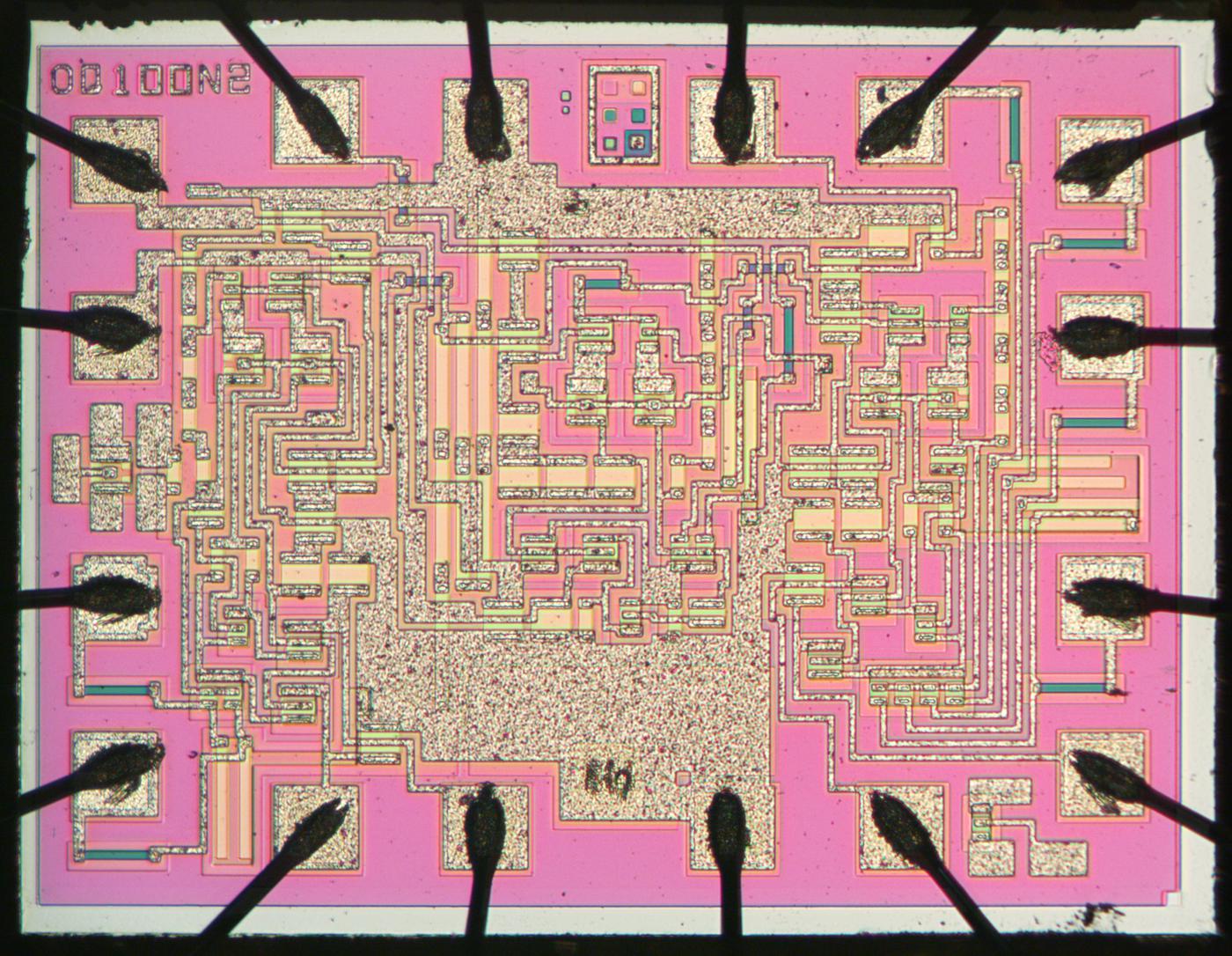
Die photo of the Philips QC100 chip. Click this photo (or any other) for a larger version. Photo courtesy of EvilMonkeyDesignz.

Die photo of the Philips QC100 chip. Click this photo (or any other) for a larger version. Photo courtesy of EvilMonkeyDesignz.

The die photo above shows the chip under the microscope. Most of the silicon appears bright pink in this image. Regions of silicon with different doping appear green or yellowish and form the transistors and resistors of the chip. The speckled regions are the metal layer on top of the silicon, wiring the circuitry together. Around the edges, the black bond wires connect the chip to the external pins.

The chip's components

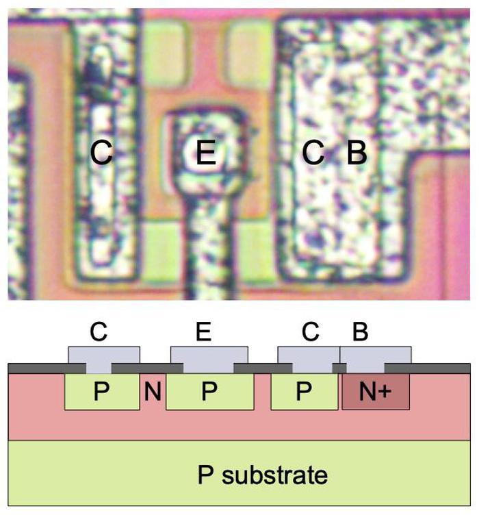
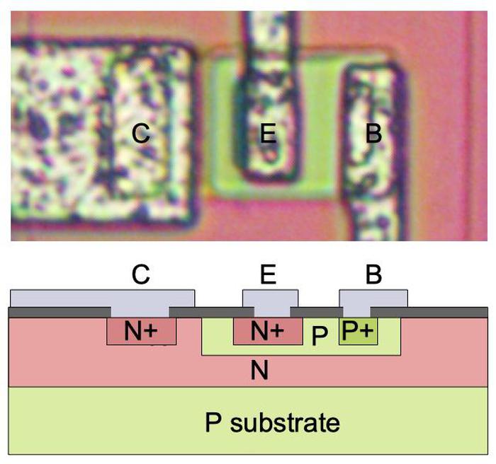
Transistors are the key components in a chip. This chip uses a type of transistor called an NPN transistor. The photo below shows a transistor as it appears on the chip. Underneath the photo is a cross-section drawing showing approximately how the transistor is constructed. The transistor is more complicated than the N-P-N sandwich you see in books, but if you look carefully at the vertical cross-section below the 'E', you can find the N-P-N layers that form the transistor. The emitter (E) wire is connected to N+ silicon. Below that is a P layer connected to the base contact (B). And below that is an N layer connected to the collector (C).

Structure of an NPN transistor. Top: transistor as it appears on the die. Bottom: cross-section diagram.

Structure of an NPN transistor. Top: transistor as it appears on the die. Bottom: cross-section diagram.

The chip also uses a few PNP transistors. Although you might expect a PNP transistor to simply be the reverse of an NPN transistor, it has a different structure, with the regions arranged laterally instead of vertically. The collector and base form concentric square rings around the emitter. The base wire is not connected to the base region directly. Instead, the wire is at a distance, and the base signal travels underneath through the N layer.

Structure of a PNP transistor. Top: transistor as it appears on the die. Bottom: cross-section diagram.

Structure of a PNP transistor. Top: transistor as it appears on the die. Bottom: cross-section diagram.

The PNP transistors in this chip have another complication. The collector is split, so the transistor has two collectors. Moreover, one of the collectors is wired directly to the base. In the photo above, you can see how the collector region is split vertically, so there is one collector on the left and one on the right, with collector on the right connected to the base. This construction may seem bizarre, but it is common in integrated circuits. The motivation is to build a current mirror, where both collectors pass the same current.

The other key components of this chip are the resistors. The photo below shows two resistors as they appear on the die. The resistors are formed from strips of higher-resistance P silicon, which appears pink in the die photos. Each end of a resistor is connected to the metal layer; the metal in the middle connects the two resistors together in series. (A metal wire also passes over the resistor but is not connected.) A resistor has higher resistance if it is longer and narrower, so these resistors have relatively high resistance.2 Resistors are relatively large on an integrated circuit and fairly inaccurate.

Two resistors as they appear on the die.

Two resistors as they appear on the die.

The circuitry

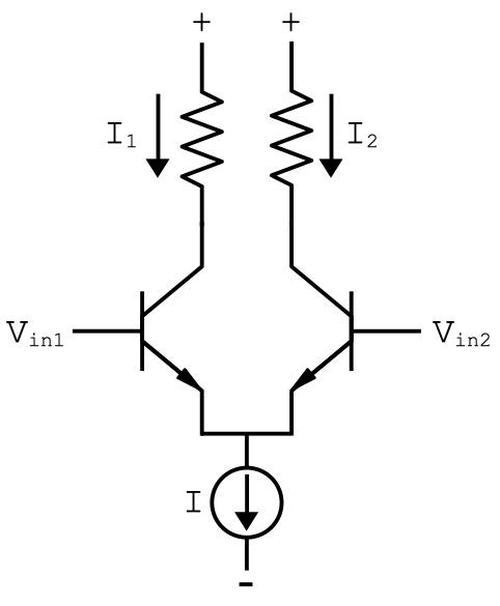
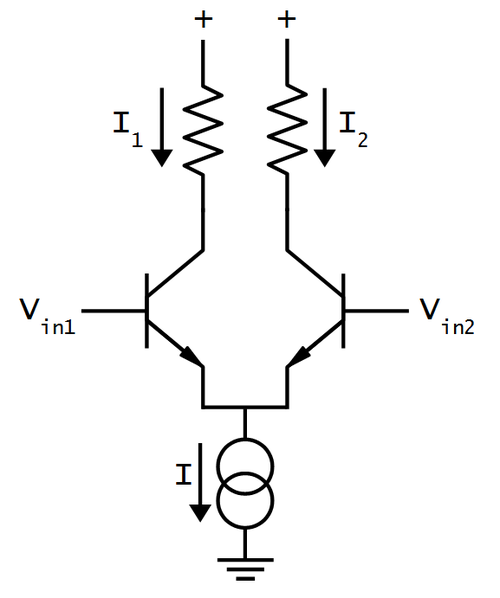
Once the components can be recognized on the die, the circuit can be traced out and reverse-engineered. But before I describe the complete circuit, I'll explain how ECL (Emitter-Coupled Logic) works.3 The schematic below shows a differential pair, or long-tailed pair, which amplifies the difference between its two inputs. (This circuit is also common in analog circuits, forming the heart of an op-amp.) The basic idea is that a current sink (the circle at the bottom) generates a fixed current I. This current gets split between the left path (I1) and the right path (I2). If the transistor on the left has a higher input voltage than the transistor on the right, most of the current will go to the left. But if the transistor on the right has a higher input, most of the current will go to the right. This circuit amplifies the voltage difference: even a small difference between the two inputs will switch most of the current from one side to the other.

Schematic of a simple differential pair circuit. The current sink sends a fixed current I through the differential pair. If the two inputs are equal, the current is split equally between the two branches. Otherwise, the branch with the higher input voltage gets most of the current.

Schematic of a simple differential pair circuit. The current sink sends a fixed current I through the differential pair. If the two inputs are equal, the current is split equally between the two branches. Otherwise, the branch with the higher input voltage gets most of the current.

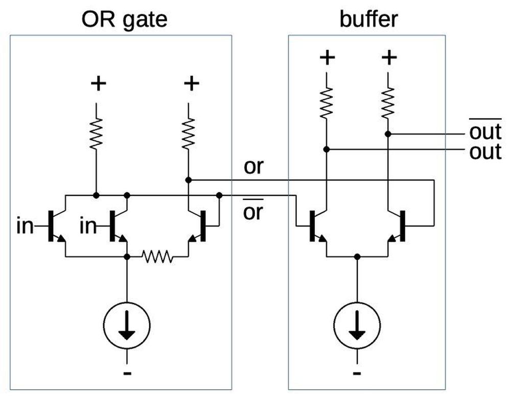
To make this into an OR gate, we can put multiple transistors on the left. If any input is high, the current will be switched to the left, otherwise the current will be switched to the right. Since the current pulls that side low, the left branch will be the NOR output while the right branch will be the OR output. (With ECL, you get both the complemented and uncomplemented outputs "for free".) The schematic below shows how one logic gate is implemented; this is a two-input gate. The gate uses a second differential pair to buffer and amplify the outputs. The current sink circuit is discussed in a footnote.4

Schematic of one logic gate.

Schematic of one logic gate.

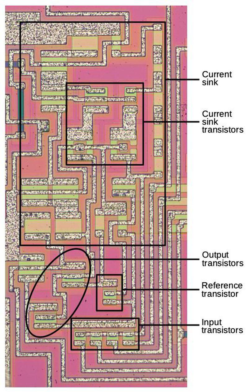
The diagram below shows how the four-input gate is implemented on the die. The majority of the area is occupied by the current sink and the associated resistors. The NPN and PNP transistors are relatively compact, but the resistors occupy a lot of space. At the bottom, the four input transistors implement the OR function, along with the reference transistor on the other branch. The output transistors are larger so they can provide more current.

One gate with functional blocks labeled.

One gate with functional blocks labeled.

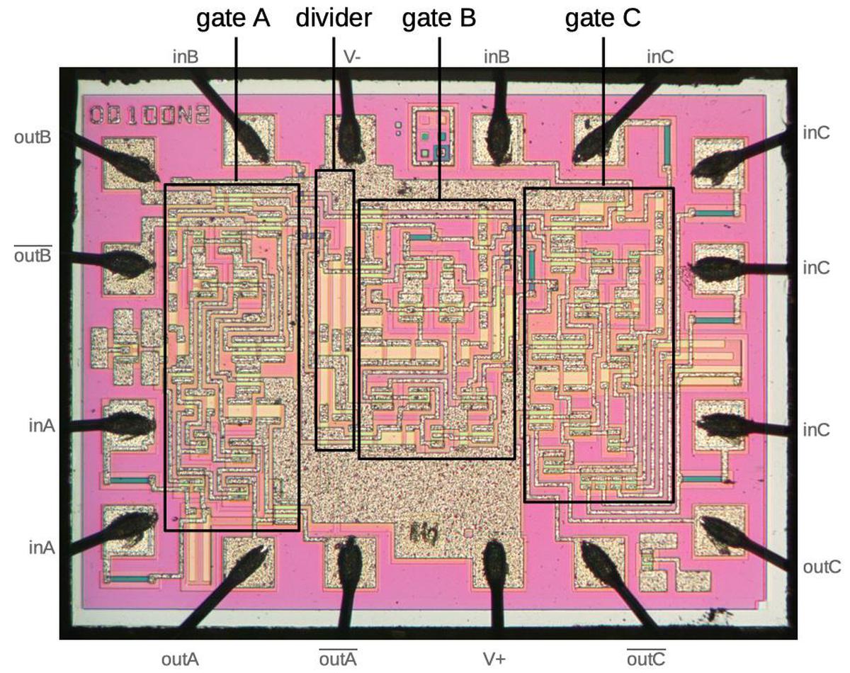
The diagram below shows how the three gates are arranged on the die. (The gate described above is at the right.) The voltage divider resistors provide a voltage reference for the current sources.

The die with major functional blocks labeled.

The die with major functional blocks labeled.

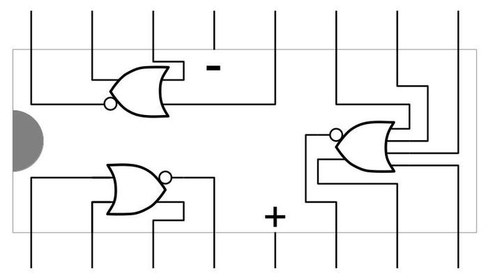
Putting everything together, the diagram below shows how the circuitry of the chip maps onto its 16 pins. The three OR gates are represented by the OR symbols; the gate on the right has four inputs. Each gate has a non-inverted output and an inverted output, which is indicated by a bubble. I don't know what voltages the chip takes, so I've indicated the power pins with + and -.

Reverse-engineered pinout of the chip.

Reverse-engineered pinout of the chip.

I announce my latest blog posts on Twitter, so follow me @kenshirriff. Many thanks to EvilMonkeyz Designs for providing the photos; follow on Instagram or Twitter for more interesting die photos.

Notes

  1. A reader said that Philips used the OQ designation for their custom integrated circuits. That would explain why I was unable to find these chips in a databook. 

  2. The resistance of a resistor is proportional to the length divided by the width. To understand this, note that a region twice as long is the same as two resistors in series, so it has twice the resistance. A region twice as wide is the same as two resistors in parallel, so it has half the resistance. 

  3. The logic circuit on this chip has a couple of differences from standard ECL gates. A typical ECL gate has inputs on one branch and a reference voltage connected to the transistor on the other branch. Thus, an input higher than the reference voltage is a logic 1, and an input lower than the reference voltage in a logic 0. This gate, however, uses the output of the first branch as the input to the second branch. If an input is high, it pulls this output low, shutting off the other branch. Conversely, if the input is low, the output goes high, turning on the other branch.

    I'm not sure what the motivation is for this design. It looks a bit like NTL (Non-Threshold Logic), since there isn't a threshold set by a reference voltage. One possibility is that the circuit implements a Schmitt-trigger, a circuit with hysteresis, where once it turns on, the input must drop significantly lower to turn it off.

    The second difference between this circuit and a typical ECL gate is the output buffer. ECL gates typically use an emitter follower, rather than a second differential pair. 

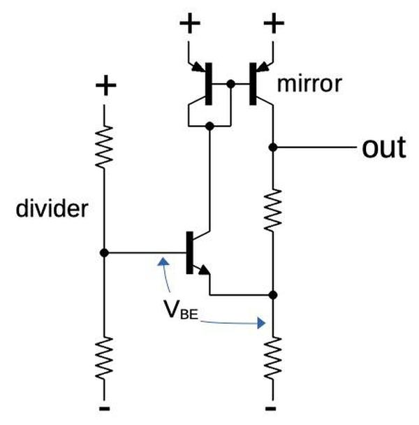
  4. I'll just briefly describe the current sink circuit, shown below. Two large resistors form a voltage divider that produces a reference voltage midway between the two supply voltages (maybe 0 volts). Due to the behavior of transistors, VBE will be one diode drop (~0.7 V). The rest of the circuit generates the "correct" current through the lower-right resistor to achieve this voltage drop. On the chip, the two PNP transistors at the top are one transistor with two collectors. They implement a current mirror, where the current through the right transistor matches the current through the left transistor.

    The current sink circuit used in the chip. The divider is shared by all the current sinks on the chip.

    The current sink circuit used in the chip. The divider is shared by all the current sinks on the chip.


Reverse-engineering a vintage comparator chip

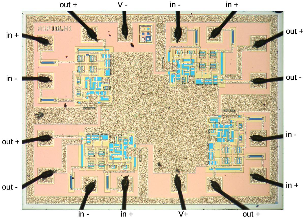
I recently saw an interesting die photo of an unknown chip on Twitter, so I did some analysis of it. Looking at the circuitry inside, the chip appears to be four comparators, probably in the ECL (Emitter Coupled Logic) family. This is a quick blog post to summarize my investigation.

The die photo below shows the chip under the microscope. Regions of the silicon appear pink, blue, or yellow, depending on how the silicon was doped. The speckled regions are the metal layer on top of the silicon, wiring the circuitry together. Around the edges, the black bond wires connect the chip to the external pins. These wires are attached to the square bond pads. The die has four blocks of circuitry, one for each of its four comparators. Much of the die is unused, especially the large metal area in the middle. Because this chip's circuitry is relatively simple, it only uses a fraction of the available space.

The chip with pins labeled.  Click this photo (or any other) for a larger version. Photo courtesy of EvilMonkeyDesignz.

The chip with pins labeled. Click this photo (or any other) for a larger version. Photo courtesy of EvilMonkeyDesignz.

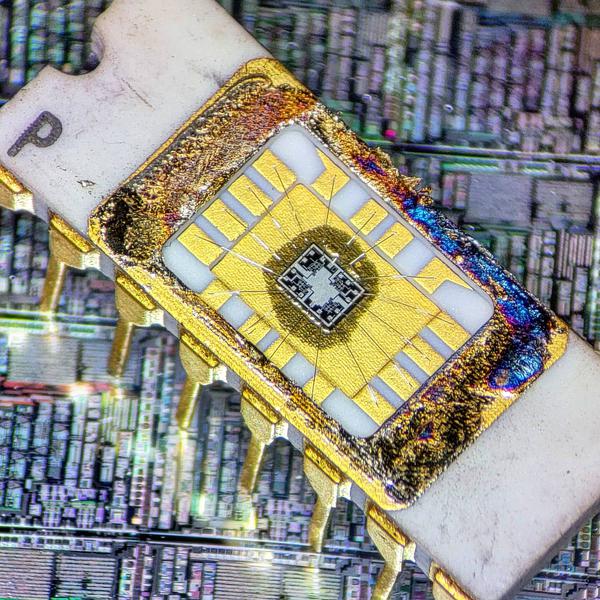
The photo below shows the chip with its metal lid removed. Modern chips are usually in a black epoxy package, but this chip has a white ceramic package. The tiny silicon die is visible in the middle, with bond wires connecting the die to the lead frame, the metal connections to the chip's gold-plated pins. The metal layer on top of the die is visible, and can be matched with the die photo above. The semi-circular notch on the left indicates the orientation of the chip; the "P" is pin 1.

The chip with the metal lid removed, showing the tiny silicon die inside.  Photo courtesy of EvilMonkeyDesignz.

The chip with the metal lid removed, showing the tiny silicon die inside. Photo courtesy of EvilMonkeyDesignz.

The chip's components

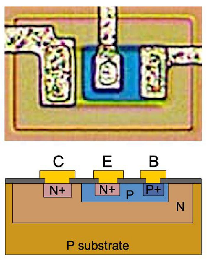
Transistors are the key components in a chip. This chip uses a type of transistor called the NPN transistor. The photo below shows a transistor as it appears on the chip. The orange and blue colors are regions of silicon that have been doped differently, forming N and P regions. The speckled areas are the metal layer of the chip on top of the silicon—these form the wires connecting to the transistor's collector, emitter, and base.

Underneath the photo is a cross-section drawing showing approximately how the transistor is constructed. There's a lot more than just the N-P-N sandwich you see in books, but if you look carefully at the vertical cross-section below the 'E', you can find the N-P-N that forms the transistor. The emitter (E) wire is connected to N+ silicon. Below that is a P layer connected to the base contact (B). And below that is an N+ layer connected (indirectly) to the collector (C). The emitter, base, and collector can be distinguished on the die with careful examination. The base's region surrounds the emitter, forming a blue rectangle. The collector contact is larger and off to the side.

Structure of an NPN transistor. Top: transistor as it appears on the die. Bottom: cross-section diagram.

Structure of an NPN transistor. Top: transistor as it appears on the die. Bottom: cross-section diagram.

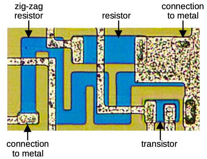
The other key components of this chip are the resistors. The photo below shows two resistors as they appear on the die. The resistors are formed from strips of higher-resistance P silicon, which appears blue in the die photos. The two ends of each resistor are connected to the metal layer. A resistor has higher resistance if it is longer and narrower. While one resistor below is a simple rectangle, the other has a complex zig-zag shape to fit more length into the available space. (The blue rectangle in the lower right is a transistor, not a resistor. To distinguish it from a resistor, note that it has three contacts, and the two contacts on the rectangle are not symmetrical.)

Two resistors as they appear on the die.

Two resistors as they appear on the die.

The circuitry

Once the components can be recognized on the die, the circuit can be traced out and reverse-engineered. But before I describe the complete circuit, I'll explain one important functional block.

The schematic below shows a differential pair, or long-tailed pair, which amplifies the difference between its two inputs. This circuit is common in analog circuits, forming the heart of an op-amp. It is also the basis of Emitter-Coupled Logic (ECL). The basic idea is that a current sink (the two circles at the bottom) generates a fixed current I. This current gets split between the left path (I1) and the right path (I2). If the transistor on the left has a higher input voltage than the transistor on the right, most of the current will go to the left. But if the transistor on the right has a higher input, most of the current will go to the right. This circuit amplifies the voltage difference: even a small difference between the two inputs will switch most of the current from one side to the other.

Schematic of a simple differential pair circuit. The current sink sends a fixed current I through the differential pair. If the two inputs are equal, the current is split equally between the two branches. Otherwise, the branch with the higher input voltage gets most of the current.

Schematic of a simple differential pair circuit. The current sink sends a fixed current I through the differential pair. If the two inputs are equal, the current is split equally between the two branches. Otherwise, the branch with the higher input voltage gets most of the current.

In this chip, the circuit is used as a comparator, a circuit that compares the two inputs and generates a logic output that indicates which input is higher. The side with the current will get pulled low, while the other side is pulled high by the resistor. Thus, the output can be treated as a logic signal.

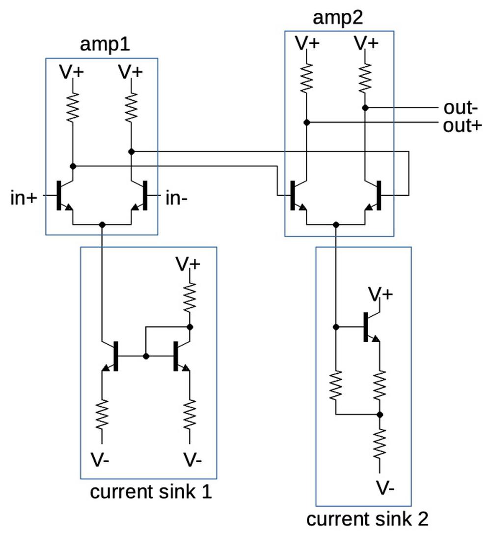
The schematic below shows the circuitry for one of the four comparators on the chip. Note that the differential amplifier circuit above is used twice. For better performance, the output from the first differential amplifier is fed into a second differential amplifier. This sharpens the output: if the inputs are close together, the outputs from the first stage may not be fully "0" or "1". The second stage amplifies this difference, providing solid "0" and "1" outputs. The current sinks provide a relatively constant current for the amplifiers, but I won't explain them in detail.

Schematic of one comparator.

Schematic of one comparator.

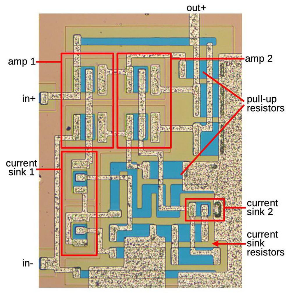
The diagram below shows the circuitry on the die, corresponding to the schematic above. The red boxes indicate the transistors for the two amplifier stages and their associated current sinks. The other components are the resistors, which appear as blue rectangles. The wiring in the metal layer connects the components together, as well as the inputs on the left and the output at the top.

One comparator, as it appears on the die.

One comparator, as it appears on the die.

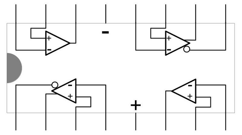
The diagram below shows how the circuitry of the chip maps onto its 16 pins. Each triangle represents a comparator with its positive and negative inputs. Two of the comparators have a single output, while two also have an inverted output (indicated by a bubble).

Reverse-engineered pinout of the chip.

Reverse-engineered pinout of the chip.

Conclusion

So what is this chip? Maybe it's simply four comparators, but they could have a specific purpose. The chip could be a converter for four differential input signals, e.g. DCS (Differential Current Switch) logic. Another chip in the family seems to be Emitter-Coupled Logic, so this chip could be four ECL inverters (but it doesn't make sense to have four pins for the reference voltage). It's a bit puzzling that two comparators have inverted and noninverted outputs, while two have single outputs.

Based on the circuitry and ceramic packaging of this chip, I estimate that it is from around 1970. The chip is labeled "OQ104", so I did a bunch of searching through old databooks, but I couldn't find anything that matches it. Since the chip looks like ECL and has the part number 104, it's tempting to think that the chip might be the 10,104 part in the MECL 10,000 series. Unfortunately, the 10,104 is a quad AND gate, and the internal circuitry is different. The "P" on the chip might indicate Philips, but I couldn't find any matching Philips components. For now, the exact identity of this chip is a mystery.

I announce my latest blog posts on Twitter, so follow me @kenshirriff. Many thanks to EvilMonkeyz Designs for providing the photos; follow on Instagram or Twitter for more interesting die photos.