HP Nanoprocessor part II: Reverse-engineering the circuits from the masks

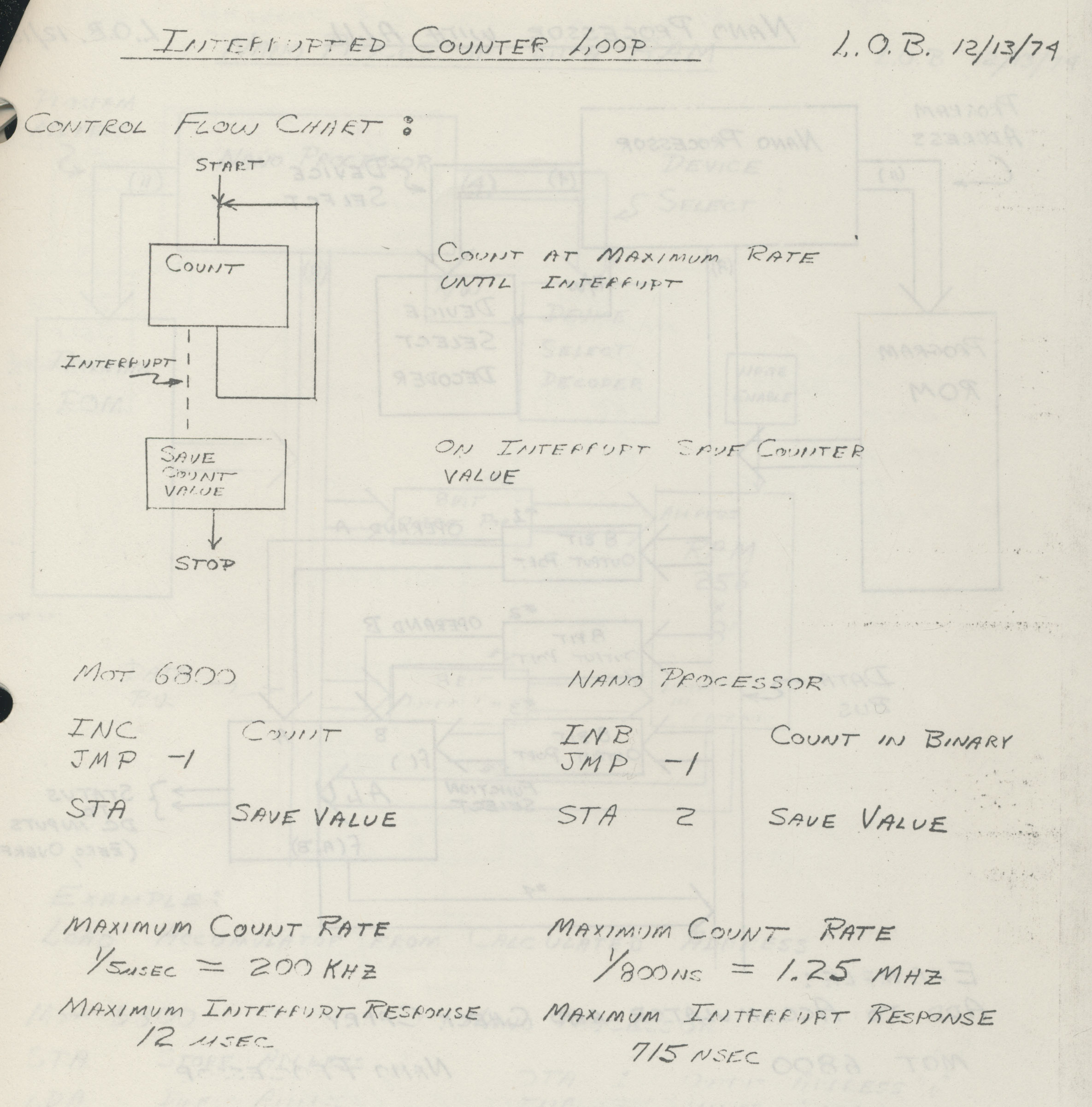
In 1974, Hewlett-Packard developed a microprocessor for control applications in their products, from floppy disk drives to voltmeters. This simple processor was a step down from the typical microprocessor—it didn't even support addition or subtraction1—so it was called the Nanoprocessor. The Nanoprocessor's key features were its low cost and high speed: compared against the contemporary Motorola 6800, the Nanoprocessor cost $15 instead of $360 and performed control tasks an order of magnitude faster.

This processor remained obscure for decades until its designer, Larry Bower, recently donated the chip's masks and documentation to The CPU Shack, who scanned the masks and wrote about the Nanoprocessor. After Antoine Bercovici stitched together the images,2 I wrote a Nanoprocessor overview article based on them. This blog post is part two, where I discuss some of the Nanoprocessor circuitry in detail, reverse-engineering it from the masks. These functional blocks are interesting to study because the Nanoprocessor strips its implementation down to the minimum, while still remaining a useful microprocessor.

The HP Nanoprocessor, part number 1820-1691. Note the hand-written bias voltage "-2.5 V", which varies from chip to chip. The last digit (1) of the part number is also hand-written, indicating
the speed of the chip. Photo courtesy of Marc Verdiell.

The HP Nanoprocessor, part number 1820-1691. Note the hand-written bias voltage "-2.5 V", which varies from chip to chip. The last digit (1) of the part number is also hand-written, indicating the speed of the chip. Photo courtesy of Marc Verdiell.

Inside the Nanoprocessor

Like most processors of that era, the Nanoprocessor was an 8-bit processor. However, it didn't support RAM,3 but ran code from an external 2-kilobyte ROM. It contained 16 8-bit registers, more than most processors and enough to make up for the lack of RAM in many applications. The Nanoprocessor had 48 instructions, a considerably smaller instruction set than the Motorola 6800's 72 instructions. However, the Nanoprocessor included convenient bit set, clear, and test operations, which other processors of that era lacked. It also had multiple I/O instructions supporting both I/O ports and general-purpose I/O pins, making it easy to control devices with the Nanoprocessor.

Combined masks from the Nanoprocessor. Click for larger image. Files courtesy of Antoine Bercovici using scans from The CPU Shack.

Combined masks from the Nanoprocessor. Click for larger image. Files courtesy of Antoine Bercovici using scans from The CPU Shack.

The mask image above shows the simplicity of the Nanoprocessor. The blue lines show the metal wiring on top of the chip, while the green shows the doped silicon underneath. The black squares around the outside are the 40 pads for connection to the IC's external pins. The small black regions inside the chip are transistors; if you squint, you should be able to count 4639 of them.4

The block diagram below shows the internal structure of the Nanoprocessor. The 16 storage registers are in the middle. The comparator allows two values to be compared for conditional branches. The Control Logic Unit performs increments, decrements, shifts, and bit operations on the accumulator, lacking the arithmetic and logical operations of a standard Arithmetic/Logic Unit (ALU). The program counter (right) fetches an instruction into the instruction register (left); interrupts and subroutine calls each have a one-entry stack for the return address.

Block diagram, from the Nanoprocessor User's Guide.

Block diagram, from the Nanoprocessor User's Guide.

I should emphasize that despite its simplicity5 and lack of arithmetic, the Nanoprocessor is not a "toy" processor that just toggles some control lines, but a fast and capable processor used for complex tasks. The HP 98035 real-time clock module, for instance, uses the Nanoprocessor to parse two dozen different ASCII command strings, as well as activities such as calculating the number of days in each month.

Registers

The die photo below shows that much of the Nanoprocessor's die is occupied by its 16 registers. These registers communicate with the rest of the chip via the data bus. Circuitry above the registers selects a particular register. Register R0, on the right, is next to the comparator, which will be important later.

The registers take up a large fraction of the Nanoprocessor's die.
Underlying die photo by Pauli Rautakorpi, CC BY 3.0.

The registers take up a large fraction of the Nanoprocessor's die. Underlying die photo by Pauli Rautakorpi, CC BY 3.0.

The building block for the registers is two inverters in a feedback loop, storing a single bit as shown below. If the top wire has a 0, the right inverter will output a 1 to the bottom wire. The left inverter will then output a 0 to the top wire, completing the cycle. Thus, the circuit is stable and will "remember" the 0. Likewise, if the top wire is a 1, this will get inverted to a 0 at the bottom wire, and back to a 1 at the top. Thus, this circuit can store either a 0 or a 1, forming a 1-bit memory.

Two inverters implement a stable loop that stores a bit.

Two inverters implement a stable loop that stores a bit.

The diagram below shows how this two-inverter storage is implemented on the die. The left shows the physical layout, from the mask images. The layout is optimized to make the cell as small as possible. Blue lines indicate the metal layer, while green is the silicon layer. The schematic in the middle shows the corresponding transistor circuitry. Each inverter is formed from a pair of transistors, as shown on the right. The top and bottom transistors are "pass transistors", providing access to the storage cell.

One bit of storage in the Nanoprocessor. Each bit is implemented by 6 transistors (also known as a 6T SRAM cell).

One bit of storage in the Nanoprocessor. Each bit is implemented by 6 transistors (also known as a 6T SRAM cell).

The register set is built from a matrix of these bit cells. The register select line selects one register (one column) for reading or writing. When selected, the top and bottom pass transistors connect the inverters to the corresponding horizontal bitlines. For a read operation, the top bitline provides the value stored in the cell; there are eight pairs of bitlines for the eight bits in a register. For a write operation, the value is applied to the upper bitline and the inverted value is applied to the lower bitline. These values overpower the signals from the inverters, forcing the inverters to the desired value and storing the bit. Thus, the grid of horizontal bitlines and vertical select lines allows a particular register to be read or written.

Instruction decoding

The instruction decoding circuitry is responsible for taking a binary instruction code (such as 01101010) and determining what instruction it is ("Load accumulator from register 10" in this case). Compared to many processors, the Nanoprocessor's instructions are pretty simple: it has relatively few instructions (48) and the opcode is always one byte long. The diagram below shows that instruction decoding logic (red) takes up a large fraction of the chip. The instruction register (green), is a set of eight latches holding the current instruction. The instruction register is next to the data pins, which provide the instruction from the ROM. This section will focus on the decoding circuit in the yellow box.

A large part of the chip is devoted to instruction decoding (red). This section will focus on the circuit highlighted in yellow. Underlying die photo by Pauli Rautakorpi, CC BY 3.0.

A large part of the chip is devoted to instruction decoding (red). This section will focus on the circuit highlighted in yellow. Underlying die photo by Pauli Rautakorpi, CC BY 3.0.

Decoding is done by NOR gates; each NOR gate detects a particular instruction or group of instructions. The NOR gates take instruction bits or their complements as inputs. When all inputs are zero, the NOR gate indicates a match. This allows matching against the entire instruction or part of the instruction. For instance, the "Load accumulator from register R" instruction has the binary format "0110rrrr", where the last four bits indicate the desired register. A NOR gate (bit7 + bit6' + bit5' + bit4)' will match instructions of that form.

The nice thing about structuring the instruction decoder in this way is that it can be built from compact, regular circuits, often called a PLA.6 The idea is to make a matrix with input signals running horizontally and outputs vertically. Each intersection can have a transistor, making the input signal part of the gate; or no transistor, ignoring that input signal. The result is tightly-packed NOR gates.

The diagram on the right below zooms in on the three decoders highlighted in yellow above. The schematic corresponds to the leftmost decoder; note the correspondence between transistors in the schematic and the pink transistor blobs in the layout. The idea is that if any input energizes a transistor, the transistor will pull the output to ground. Otherwise, the output is pulled high by the resistor. The inverters at the bottom amplify the signal, providing enough current to drive all eight slices of the accumulator.7 Curiously, the layout uses pairs of transistors, both connected between ground and the output; I don't see the advantage over the straightforward approach of using a single transistor. In any case, note how the PLA-style matrix provides a dense layout for the decoders.

This diagram shows one of the decoder circuits in the Nanoprocessor. The schematic corresponds to the leftmost decoder of the three shown on the right.

This diagram shows one of the decoder circuits in the Nanoprocessor. The schematic corresponds to the leftmost decoder of the three shown on the right.

This particular circuit generates the increment/decrement signal that is fed into the accumulator circuit. This circuit matches when the clock, fetch, instruction bit 6, and instruction bit 2 are all low, so it matches instructions of the form x0xxx0xx during execute phase. These instructions include "Increment Binary" (00000000), "Increment BCD" (00000010), "Decrement Binary" (00000001) and "Decrement BCD" (00000011).8

Comparator

An important circuit in the Nanoprocessor is the comparator that determines if the accumulator A is greater, less than, or equal to register R0. The comparator uses a simple but clever circuit to compare these two values. The algorithm is essentially to compare the two numbers starting with the most significant bits. As long as the bits are equal, keep moving to the less significant bits. The first difference between the two numbers determines which one is greater. (For instance, with 10101010 and 10100111, the highlighted bits determine that the first number is greater.)

This algorithm is implemented with eight stages, one for each bit, starting with the most significant bits at the bottom. Each stage (below) consists of two symmetrical parts: one determines if A > R0, while the complementary one determines if A < R0. If the numbers are equal so far, but the two bits are different at this stage, the stage generates the greater than or less than signal. Otherwise, it passes along the decision of the lower stage. The topmost stage outputs the final decision. Note that the comparator provides an equality test "for free"; if the output isn't greater than or less than, the two numbers are equal.

One stage of the 8-bit comparator.

One stage of the 8-bit comparator.

The diagram below shows the physical layout of two comparator stages. One clever feature of the comparator's layout is that it sits between register 0 on the left and the accumulator on the right, minimizing wiring. The comparator accesses register 0 directly, without going through the regular path of the register selection and the data bus.

Two stages of the comparator, as it appears in the masks.

Two stages of the comparator, as it appears in the masks.

The Nanoprocessor's conditional branch instructions can test the comparator outputs.9 The branch circuitry is fairly straightforward: several bits of the branch instruction select the particular test via a multiplexer. Then bit 7 of the instruction selects "branch if true" versus "branch if false". Unlike most processors, the Nanoprocessor doesn't provide branches to an arbitrary address. Instead, it skips two instruction bytes if the condition is satisfied. (Typically these two bytes would hold a jump to the desired target, but sometimes hold other instructions.) The skip circuit is simple: the program counter incrementer (described below) is triggered a second time, but increments by two instead of one, skipping two instructions. Thus, the Nanoprocessor implements an extensive set of conditional tests with a relatively small amount of circuitry.

Accumulator and Control Logic Unit

The accumulator is the special 8-bit register that stores the byte currently being processed. Operations on the accumulator are performed by the Control Logic Unit (CLU), which the manual calls "the heart of the Nanoprocessor". The CLU is the equivalent of the Arithmetic/Logic Unit (ALU) in most processors, except it doesn't perform arithmetic or logic operations. The CLU is not quite as useless as it sounds, though. It can increment or decrement the accumulator, both in binary and binary coded decimal (BCD). (Binary coded decimal stores two decimal digits per byte. This is very useful for decimal I/O or displays.) The CLU can also complement or clear the accumulator, or set or clear a specific bit. Finally, it supports left and right shift operations.

Circuitry related to the accumulator.
Underlying die photo by Pauli Rautakorpi, CC BY 3.0.

Circuitry related to the accumulator. Underlying die photo by Pauli Rautakorpi, CC BY 3.0.

The diagram above shows the layout of the accumulator and CLU. The first region has miscellaneous circuitry to detect a zero value; support BCD by detecting a 9 digit, for instance; and provide carry-skip, fast carry generation from the lower 4 bits. I won't discuss this in more detail, but note the irregular layout of this circuitry. The second region holds the main accumulator and CLU circuitry; I will discuss this in detail below. The third region distributes control signals from the decode logic above to the eight accumulator slices. Finally, the last region holds instruction decoding logic to decode bit operations and signal the appropriate accumulator slice.

The main part of the accumulator/CLU consists of 8 slices, one for each bit, with the lowest bit at the top. I will discuss four circuits in each slice: the incrementer/decrementer's carry generation, the incrementer/decrementer's bit generation, the multiplexer to select the new accumulator value, and the latch that holds the accumulator's value.

Each slice of the incrementer/decrementer (below) is implemented by a half adder. The direction of the incrementer/decrementer circuit depends on the opcode: a 0 in the opcode's low bit indicates an increment, while a 1 in the opcode's low bit indicates a decrement. The carry circuit on the left below generates the carry-out signal. For an increment, there is a carry-out if there is a carry-in and the current bit is 1 (since it will be incremented to binary 10). For decrement, the carry line indicates a borrow, rather than a carry, so there is a carry-out if there is a carry-in (i.e. a borrow) and the current bit is 0, triggering a borrow.

One slice of the incrementer/decrementer circuit.

One slice of the incrementer/decrementer circuit.

The circuit on the right above updates the current bit when incrementing or decrementing. The current bit is flipped if there is a carry-in, essentially an XOR implemented by three NOR gates. One complication is the adjustment for BCD (binary-coded decimal). For a BCD increment operation, a carry occurs when incrementing a 9 digit, while for a BCD decrement, a 0 digit is decremented to 9, not to binary 1111.

The different accumulator operations are provided by the multiplexer below. Depending on the operation, one pass transistor will be activated, selecting the desired value. For instance, for an increment/decrement operation, the top transistor selects the output from the increment/decrement circuit described above. This transistor is activated by the instruction decoder described earlier that matches an increment/decrement instruction. Similarly, a shift-right instruction activates the shift-right pass transistor, feeding accumulator bit n+1 into each accumulator slice to shift the value.

Schematic of the latch holding one bit of the accumulator, along with the multiplexer that selects an input to the accumulator.

Schematic of the latch holding one bit of the accumulator, along with the multiplexer that selects an input to the accumulator.

The latch above stores one bit of the accumulator. When the hold accumulator transistor is activated, the two NOR gates form a loop, holding the value. But when the load accumulator transistor is activated instead, the accumulator loads its value from the multiplexer. The clear bit n and set bit n lines allow instructions to modify individual bits of the accumulator; the multiplexer, in comparison, updates all accumulator bits at once.

Program counter and addressing

Another large block of circuitry is the 11-bit program counter in the lower left of the Nanoprocessor, which I'll describe briefly. This block also includes a latch to hold the return address for a subroutine call and a second latch to hold the program counter after an interrupt. (You can think of these as one-entry stacks.) The program counter includes an incrementer to advance it to the next instruction. This incrementer can also increment by two, allowing conditional branch instructions to skip over two instructions. (Increment-by-two is implemented by incrementing bit 1 instead of bit 0.) To improve the performance of the incrementer, it has a carry-skip feature; if the bottom six bits are all 1, it will increment bit 6 immediately without waiting for the carry to propagate through the low-order bits.

Control and timing

The final piece of the Nanoprocessor is the control circuitry. Compared to other microprocessors, the Nanoprocessor's control circuitry is almost trivial: the processor alternates between fetch and execute cycles (with the occasional interrupt). The control circuitry is not much more than a couple of flip flops and gates, so I won't say more about it.

Conclusions

The diagram below summarizes the main functional blocks of the Nanoprocessor. The Nanoprocessor achieves a dense layout for these blocks, much better than I would expect from its obsolete metal-gate technology.10 Reverse-engineering shows that these functional blocks are implemented with simple but carefully-designed circuits.

Functional components of the HP Nanoprocessor, based on my reverse-engineering.
Underlying die photo by Pauli Rautakorpi, CC BY 3.0.

Functional components of the HP Nanoprocessor, based on my reverse-engineering. Underlying die photo by Pauli Rautakorpi, CC BY 3.0.

The Nanoprocessor is an unusual processor. My first impression was that it wasn't even a "real processor," since it lacked basic arithmetic functionality. However, after studying it, I'm more impressed. Its simple design allows it to operate faster than other processors of the time. The instruction set is more capable than it appears at first. Hewlett-Packard used the Nanoprocessor in many products in the 1970s and 1980s, in roles that were more complex than you'd expect, such as parsing strings and performing calculations. Now, with the masks released by The CPU Shack, we can learn the secrets of the circuits that made the Nanoprocessor work.

Nanoprocessor (white chip) as part of an HP clock module.
Note the hand-written voltage on the chip; each chip required a different bias voltage.
Photo courtesy of Marc Verdiell.

Nanoprocessor (white chip) as part of an HP clock module. Note the hand-written voltage on the chip; each chip required a different bias voltage. Photo courtesy of Marc Verdiell.

Follow me on Twitter at @kenshirriff for updates on my blog posts. I also have an RSS feed. Thanks to Antoine Bercovici for scanning and remastering the masks, Larry Bower for the donation, and John Culver at The CPU Shack for sharing the donation.

Notes and references

  1. Although it lacks an addition instruction, the Nanoprocessor can add numbers (slowly) through repeated increment and decrement operations (which it supports). (The code for the HP real-time clock module does this.) Other applications, such as the HP voltmeter, added external ALU chips (74LS181) to perform fast addition; these were accessed as I/O devices. (With Turing-completeness, of course, the Nanoprocessor can theoretically do anything from floating-point functions to Crysis; it will just be very slow.) 

  2. The mask images can be downloaded here (warning: 122 MB PSD file). 

  3. The Nanoprocessor doesn't have instructions to support RAM, since it is designed for control applications that typically don't need much storage. However, some Nanoprocessor applications use RAM, treating RAM as an I/O device. The address is written to one I/O port and the data byte is read or written from another port. 

  4. By my count, the Nanoprocessor has 4639 transistors. The instruction decoder is constructed from pairs of small transistors for layout reasons; combining these pairs yields 3829 unique transistors. Of these, 1061 act as pull-ups, while 2668 are active. In comparison, the 6502 has 4237 transistors, of which 3218 are active. The 8008 has 3500 transistors and the Motorola 6800 has 4100 transistors. 

  5. Making an FPGA version of the Nanoprocessor would probably be a fun project since the Nanoprocessor is about as simple as you can make a real, commercial processor. The User's Guide explains the instructions and has sample code that could be executed. 

  6. Building the decoder out of an array of NOR gates decoding was common in early microprocessors, for instance the 6502, because it could be constructed in a regular, compact form. It's often called a PLA (Programmable Logic Array), even though a PLA is supposed to have two layers of logic. 

  7. Note that the inverters in the instruction decoder are pulled up to 12 volts, rather than 5 volts. The reason is that the Nanoprocessor uses metal-gate transistors, rather than the more advanced silicon-gate transistors of other microprocessors of the era. Metal-gate transistors have the disadvantage of a higher threshold voltage, which means the output of a transistor is considerably lower than the gate voltage. The output from a regular inverter is too low to drive the gate of a pass transistor, since the output will be another threshold voltage below that. The solution is to use the 12 volt supply for the decoder inverters that drive pass transistors in the accumulator. Then, these signals have plenty of voltage to drive pass transistors. In other words, the Nanoprocessor required an extra +12V supply because it used metal-gate transistors instead of the more modern silicon-gate transistors. 

  8. The illustrated decode circuit matches against instructions x0xxx0xx, so it matches against many more instructions than just the increment and decrement instructions. Why doesn't the circuit match exactly? The reason is that if the accumulator is not being used, it doesn't matter if the increment/decrement signal is activated. By making the match wider, the designers could omit some transistors. The important point is that the circuit rejects other accumulator instructions such as "Clear accumulator" (00000100) or "Load accumulator from register" (0110rrrr). 

  9. The Nanoprocessor has an extensive set of conditional branches, surprisingly many for a simple processor. You can branch if A > R0, A >= R0, A < R0, A <= R0, A == R0, or A != R0. In additional conditional branches can be done on the accumulator being zero or nonzero, any particular bit of the accumulator being zero or nonzero, the overflow flag being set or not, or a particular general-purpose I/O ("direct control") bit being set or not. 

  10. The Nanoprocessor used metal-gate transistors, while other microprocessors started using silicon-gate transistors a few years earlier. This may seem like an obscure difference, but it has a huge impact on layout: silicon-gate fabrication added a layer of polysilicon wiring. This makes layout much easier, since you now have two layers for wiring that can cross each other. With just the metal layer for wiring, like the Nanoprocessor, layout is difficult because wires keep getting in the way of each other. In other metal-gate chips that I've examined, the layout is just awful; there's a lot of convoluted wiring to get the signals to each transistor, so the transistor density is low. In comparison, the Nanoprocessor's functional blocks are all carefully designed so the signals all flow together nicely. There's some wasted space, for instance for the data bus, but overall, I'm impressed by the density of the Nanoprocessor's layout. 

Reverse-engineering the first FPGA chip, the XC2064

A Field-Programmable Gate Array (FPGA) can implement arbitrary digital logic, anything from a microprocessor to a video generator or crypto miner. An FPGA consists of many logic blocks, each typically consisting of a flip flop and a logic function, along with a routing network that connects the logic blocks. What makes an FPGA special is that it is programmable hardware: you can redefine each logic block and the connections between them. The result is you can build a complex digital circuit without physically wiring up individual gates and flip flops or going to the expense of designing a custom integrated circuit.

Die photo closeup showing the circuitry for one of the 64 tiles in the XC2064 FPGA. The metal layers have been removed, exposing the silicon and polysilicon transistors underneath. Click for a larger image. From siliconpr0n.

Die photo closeup showing the circuitry for one of the 64 tiles in the XC2064 FPGA. The metal layers have been removed, exposing the silicon and polysilicon transistors underneath. Click for a larger image. From siliconpr0n.

The FPGA was invented by Ross Freeman1 who co-founded Xilinx2 in 1984 and introduced the first FPGA, the XC2064. 3 This FPGA is much simpler than modern FPGAs—it contains just 64 logic blocks, compared to thousands or millions in modern FPGAs—but it led to the current multi-billion-dollar FPGA industry. Because of its importance, the XC2064 is in the Chip Hall of Fame. I reverse-engineered Xilinx's XC2064, and in this blog post I explain its internal circuitry (above) and how a "bitstream" programs it.

The Xilinx XC2064 was the first FPGA chip. Photo from siliconpr0n.

The Xilinx XC2064 was the first FPGA chip. Photo from siliconpr0n.

Nowadays, an FPGA is programed in a hardware description language such as Verilog or VHDL, but back then Xilinx provided their own development software, an MS-DOS application named XACT with a hefty $12,000 price tag. XACT operated at a lower level than modern tools: the user defined the function of each logic block, as shown in the screenshot below, and the connections between logic blocks. XACT routed the connections and generated a bitstream file that could be loaded into the FPGA.

Screenshot of XACT. The two lookup tables F and G implement the equations at the bottom of the screen, with Karnaugh map shown above.

Screenshot of XACT. The two lookup tables F and G implement the equations at the bottom of the screen, with Karnaugh map shown above.

An FPGA is configured via the bitstream, a sequence of bits with a proprietary format. If you look at the bitstream for the XC2064 (below), it's a puzzling mixture of patterns that repeat irregularly with sequences scattered through the bitstream. There's no clear connection between the function definitions in XACT and the data in the bitstream. However, studying the physical circuitry of the FPGA reveals the structure of the bitstream data and it can be understood.

Part of the bitstream generated by XACT.

Part of the bitstream generated by XACT.

How does an FPGA work?

The diagram below, from the original FPGA patent, shows the basic structure of an FPGA. In this simplified FPGA, there are 9 logic blocks (blue) and 12 I/O pins. An interconnection network connects the components together. By setting switches (diagonal lines) on the interconnect, the logic blocks are connected to each other and to the I/O pins. Each logic element can be programmed with the desired logic function. The result is a highly programmable chip that can implement anything that fits in the available circuitry.

The FPGA patent shows logic blocks (LE) linked by an interconnect.

The FPGA patent shows logic blocks (LE) linked by an interconnect.

CLB: Configurable Logic Block

While the diagram above shows nine configurable logic blocks (CLBs), the XC2064 has 64 CLBs. The diagram below shows the structure of each CLB. Each CLB has four inputs (A, B, C, D) and two outputs (X and Y). In between is combinatorial logic, which can be programmed with any desired logic function. The CLB also contains a flip flop, allowing the FPGA to implement counters, shift registers, state machines and other stateful circuits. The trapezoids are multiplexers, which can be programmed to pass through any of their inputs. The multiplexers allow the CLB to be configured for a particular task, selecting the desired signals for the flip flop controls and the outputs.

A Configurable Logic Block in the XC2064, from the datasheet.

A Configurable Logic Block in the XC2064, from the datasheet.

You might wonder how the combinatorial logic implements arbitrary logic functions. Does it select between a collection of AND gates, OR gates, XOR gates, and so forth? No, it uses a clever trick called a lookup table (LUT), in effect holding the truth table for the function. For instance, a function of three variables is defined by the 8 rows in its truth table. The LUT consists of 8 bits of memory, along with a multiplexer circuit to select the right value. By storing values in these 8 bits of memory, any 3-input logic function can be implemented.4

The interconnect

The second key piece of the FPGA is the interconnect, which can be programmed to connect the CLBs in different ways. The interconnect is fairly complicated, but a rough description is that there are several horizontal and vertical line segments between each CLB. CLB. Interconnect points allow connections to be made between a horizontal line and a vertical line, allowing arbitrary paths to be created. More complex connections are done via "switch matrices". Each switch matrix has 8 pins, which can be wired together in (almost) arbitrary ways.

The diagram below shows the interconnect structure of the XC2064, providing connections to the logic blocks (cyan) and the I/O pins (yellow). The inset shows a closeup of the routing features. The green boxes are the 8-pin switch matrices, while the small squares are the programmable interconnection points.

The XC2064 FPGA has an 8 by 8 grid of CLBs. Each CLB has an alphabetic name from AA to HH.

The XC2064 FPGA has an 8 by 8 grid of CLBs. Each CLB has an alphabetic name from AA to HH.

The interconnect can wire, for example, an output of block DC to an input of block DE, as shown below. The red line indicates the routing path and the small red squares indicate activated routing points. After leaving block DC, the signal is directed by the first routing point to an 8-pin switch (green) which directs it to two more routing points and another 8-pin switch. (The unused vertical and horizontal paths are not shown.) Note that routing is fairly complex; even this short path used four routing points and two switches.

Example of a signal routed from an output of block DC to block DE.

Example of a signal routed from an output of block DC to block DE.

The screenshot below shows what routing looks like in the XACT program. The yellow lines indicate routing between the logic blocks. As more signals are added, the challenge is to route efficiently without the paths colliding. The XACT software package performs automatic routing, but routes can also be edited manually.

Screenshot of the XACT program.
This MS-DOS program was controlled via the keyboard and mouse.

Screenshot of the XACT program. This MS-DOS program was controlled via the keyboard and mouse.

The implementation

The remainder of this post discusses the internal circuitry of the XC2064, reverse-engineered from die photos.5 Be warned that this assumes some familiarity with the XC2064.

The die photo below shows the layout of the XC2064 chip. The main part of the FPGA is the 8×8 grid of tiles; each tile holds one logic block and the neighboring routing circuitry. Although FPGA diagrams show the logic blocks (CLBs) as separate entities from the routing that surrounds them, that is not how the FPGA is implemented. Instead, each logic block and the neighboring routing are implemented as a single entity, a tile. (Specifically, the tile includes the routing above and to the left of each CLB.)

Layout of the XC2064 chip. Image from siliconpr0n.

Layout of the XC2064 chip. Image from siliconpr0n.

Around the edges of the integrated circuit, I/O blocks provide communication with the outside world. They are connected to the small green square pads, which are wired to the chip's external pins. The die is divided by buffers (green): two vertical and two horizontal. These buffers amplify signals that travel long distances across the circuit, reducing delay. The vertical shift register (pink) and horizontal column select circuit (blue) are used to load the bitstream into the chip, as will be explained below.

Inside a tile

The diagram below shows the layout of a single tile in the XC2064; the chip contains 64 of these tiles packed together as shown above. About 40% of each tile is taken up by the memory cells (green) that hold the configuration bits. The top third (roughly) of the tile handles the interconnect routing through two switch matrices and numerous individual routing switches. Below that is the logic block. Key parts of the logic block are multiplexers for the input, the flip flop, and the lookup tables (LUTs). The tile is connected to neighboring tiles through vertical and horizontal wiring for interconnect, power and ground. The configuration data bits are fed into the memory cells horizontally, while vertical signals select a particular column of memory cells to load.

One tile of the FPGA, showing important functional units.

One tile of the FPGA, showing important functional units.

Transistors

The FPGA is implemented with CMOS logic, built from NMOS and PMOS transistors. Transistors have two main roles in the FPGA. First, they can be combined to form logic gates. Second, transistors are used as switches that signals pass through, for instance to control routing. In this role, the transistor is called a pass transistor. The diagram below shows the basic structure of an MOS transistor. Two regions of silicon are doped with impurities to form the source and drain regions. In between, the gate turns the transistor on or off, controlling current flow between the source and drain. The gate is made of a special type of silicon called polysilicon, and is separated from the underlying silicon by a thin insulating oxide layer. Above this, two layers of metal provide wiring to connect the circuitry.

Structure of a MOSFET.

Structure of a MOSFET.

The die photo closeup below shows what a transistor looks like under a microscope. The polysilicon gate is the snaking line between the two doped silicon regions. The circles are vias, connections between the silicon and the metal layer (which has been removed for this photo).

A MOSFET as it appears in the FPGA.

A MOSFET as it appears in the FPGA.

The bitstream and configuration memory

The configuration information in the XC2064 is stored in configuration memory cells. Instead of using a block of RAM for storage, the FPGA's memory is distributed across the chip in a 160×71 grid, ensuring that each bit is next to the circuitry that it controls. The diagram below shows how the configuration bitstream is loaded into the FPGA. The bitstream is fed into the shift register that runs down the center of the chip (pink). Once 71 bits have been loaded into the shift register, the column select circuit (blue) selects a particular column of memory and the bits are loaded into this column in parallel. Then, the next 71 bits are loaded into the shift register and the next column to the left becomes the selected column. This process repeats for all 160 columns of the FPGA, loading the entire bitstream into the chip. Using a shift register avoids bulky memory addressing circuitry.

How the bitstream is loaded into the FPGA. The bits shown are conceptual; actual bit storage is much denser. The three columns on the left have been loaded and the fourth column is currently being loaded. Die photo from siliconpr0n.

How the bitstream is loaded into the FPGA. The bits shown are conceptual; actual bit storage is much denser. The three columns on the left have been loaded and the fourth column is currently being loaded. Die photo from siliconpr0n.

The important point is that the bitstream is distributed across the chip exactly as it appears in the file: the layout of bits in the bitstream file matches the physical layout on the chip. As will be shown below, each bit is stored in the FPGA next to the circuit it controls. Thus, the bitstream file format is directly determined by the layout of the hardware circuits. For instance, when there is a gap between FPGA tiles because of the buffer circuitry, the same gap appears in the bitstream. The content of the bitstream is not designed around software concepts such as fields or data tables or configuration blocks. Understanding the bitstream depends on thinking of it in hardware terms, not in software terms.7

Each bit of configuration memory is implemented as shown below.8 Each memory cell consists of two inverters connected in a loop. This circuit has two stable states so it can store a bit: either the top inverter is 1 and the bottom is 0 or vice versa. To write to the cell, the pass transistor on the left is activated, passing the data signal through. The signal on the data line simply overpowers the inverters, writing the desired bit. (You can also read the configuration data out of the FPGA using the same path.) The Q and inverted Q outputs control the desired function in the FPGA, such as closing a routing connection, providing a bit for a lookup table, or controlling the flip flops. (In most cases, just the Q output is used.)

Schematic diagram of one bit of configuration memory, from the datasheet. Q is the output and Q is the inverted output.

Schematic diagram of one bit of configuration memory, from the datasheet. Q is the output and Q is the inverted output.

The diagram below shows the physical layout of memory cells. The photo on the left shows eight memory cells, with one cell highlighted. Each horizontal data line feeds all the memory cells in that row. Each column select line selects all the memory cells in that column for writing. The middle photo zooms in on the silicon and polysilicon transistors for one memory cell. The metal layers were removed to expose the underlying transistors. The metal layers wire together the transistors; the circles are connections (vias) between the silicon or polysilicon and the metal. The schematic shows how the five transistors are connected; the schematic's physical layout matches the photo. Two pairs of transistors form two CMOS inverters, while the pass transistor in the lower left provides access to the cell.

Eight bits of configuration memory, four above and four below. The red box shows one bit. When a column select line is activated, the row data line is loaded into the corresponding cells. The closeup and schematic show one bit of configuration memory. Die photo from siliconpr0n.

Eight bits of configuration memory, four above and four below. The red box shows one bit. When a column select line is activated, the row data line is loaded into the corresponding cells. The closeup and schematic show one bit of configuration memory. Die photo from siliconpr0n.

Lookup table multiplexers

As explained earlier, the FPGA implements arbitrary logic functions by using a lookup table. The diagram below shows how a lookup table is implemented in the XC2064. The eight values on the left are stored in eight memory cells. Four multiplexers select one of each pair of values, depending on the value of the A input; if A is 0, the top value is selected and if A is 1 the bottom value is selected. Next, a larger multiplexer selects one of the four values based on B and C. The result is the desired value, in this case A XOR B XOR C. By putting different values in the lookup table, the logic function can be changed as desired.

Implementing XOR with a lookup table.

Implementing XOR with a lookup table.

Each multiplexer is implemented with pass transistors. Depending on the control signals, one of the pass transistors is activated, passing that input to the output. The diagram below shows part of the LUT circuitry, multiplexing two of the bits. At the right are two of the memory cells. Each bit goes through an inverter to amplify it, and then passes through the multiplexer's pass transistors in the middle, selecting one of the bits.

A closeup of circuitry in the LUT implementation. Die photo from siliconpr0n.

A closeup of circuitry in the LUT implementation. Die photo from siliconpr0n.

Flip flop

Each CLB contains a flip flop, allowing the FPGA to implement latches, state machines, and other stateful circuits. The diagram below shows the (slightly unusual) implementation of the flip flop. It uses a primary/secondary design. When the clock is low, the first multiplexer lets the data into the primary latch. When the clock goes high, the multiplexer closes the loop for the first latch, holding the value. (The bit is inverted twice going through the OR gate, NAND gate, and inverter, so it is held constant.) Meanwhile, the secondary latch's multiplexer receives the bit from the first latch when the clock goes high (note that the clock is inverted). This value becomes the flip flop's output. When the clock goes low, the secondary's multiplexer closes the loop, latching the bit. Thus, the flip flop is edge-sensitive, latching the value on the rising edge of the clock. The set and reset lines force the flip flop high or low.

Flip flop implementation. The arrows point out the first multiplexer and the two OR-NAND gates. Die photo from siliconpr0n.

Flip flop implementation. The arrows point out the first multiplexer and the two OR-NAND gates. Die photo from siliconpr0n.

8-pin switch matrix

The switch matrix is an important routing element. Each switch has eight "pins" (two on each side) and can connect almost any combination of pins together. This allows signals to turn, split, or cross over with more flexibility than the individual routing nodes. The diagram below shows part of the routing network between four CLBs (cyan). The switch matrices (green) can be connected with any combination of the connections on the right. Note that each pin can connect to 5 of the 7 other pins. For instance, pin 1 can connect to pin 3 but not pin 2 or 4. This makes the matrix almost a crossbar, with 20 potential connections rather than 28.

Based on Xilinx Programmable Gate Array Data Book, fig 7b.

The switch matrix is implemented by a row of pass transistors controlled by memory cells above and below. The two sides of the transistor are the two switch matrix pins that can be connected by that transistor. Thus, each switch matrix has 20 associated control bits;9 two matrices per tile yields matrix 40 control bits per tile. The photo below indicates one of the memory cells, connected to the long squiggly gate of the pass transistor below. This transistor controls the connection between pin 5 and pin 1. Thus, the bit in the bitstream corresponding to that memory cell controls the switch connection between pin 5 and pin 1. Likewise, the other memory cells and their associated transistors control other switch connections. Note that the ordering of these connections follows no particular pattern; consequently, the mapping between bitstream bits and the switch pins appears random.

Implementation of an 8-pin switch matrix. The silicon regions are labeled with the corresponding pin numbers.
The metal layers (which connect the pins to the transistors) were removed for this photo.
Based on die photo from siliconpr0n.

Implementation of an 8-pin switch matrix. The silicon regions are labeled with the corresponding pin numbers. The metal layers (which connect the pins to the transistors) were removed for this photo. Based on die photo from siliconpr0n.

Input routing

The inputs to a CLB use a different encoding scheme in the bitstream, which is explained by the hardware implementation. In the diagram below, the eight circled nodes are potential inputs to CLB box DD. Only one node (at most) can be configured as an input, since connecting two signals to the same input would short them together.

Input selection. The eight nodes circled in green are potential inputs to DD; one of them can be selected.

Input selection. The eight nodes circled in green are potential inputs to DD; one of them can be selected.

The desired input is selected using a multiplexer. A straightforward solution would use an 8-way multiplexer, with 3 control bits selecting one of the 8 signals. Another straightforward solution would be to use 8 pass transistors, each with its own control signal, with one of them selecting the desired signal. However, the FPGA uses a hybrid approach that avoids the decoding hardware of the first approach but uses 5 control signals instead of the eight required by the second approach.

The FPGA uses multiplexers to select one of eight inputs.

The FPGA uses multiplexers to select one of eight inputs.

The schematic above shows the two-stage multiplexer approach used in the FPGA. In the first stage, one of the control signals is activated. The second stage picks either the top or bottom signal for the output.10 For instance, suppose control signal B/F is sent to the first stage and 'ABCD' to the second stage; input B is the only one that will pass through to the output. Thus, selecting one of the eight inputs requires 5 bits in the bitstream and uses 5 memory cells.

Conclusion

The XC2064 uses a variety of highly-optimized circuits to implement its logic blocks and routing. This circuitry required a tight layout in order to fit onto the die. Even so, the XC2064 was a very large chip, larger than microprocessors of the time, so it was difficult to manufacture at first and cost hundreds of dollars. Compared to modern FPGAs, the XC2064 had an absurdly small number of cells, but even so it sparked a revolutionary new product line.

Two concepts are the key to understanding the XC2064's bitstream. First, the FPGA is implemented from 64 tiles, repeated blocks that combine the logic block and routing. Although FPGAs are described as having logic blocks surrounded by routing, that is not how they are implemented. The second concept is that there are no abstractions in the bitstream; it is mapped directly onto the two-dimensional layout of the FPGA. Thus, the bitstream only makes sense if you consider the physical layout of the FPGA.

I've determined how most of the XC2064 bitstream is configured (see footnote 11) and I've made a program to generate the CLB information from a bitstream file. Unfortunately, this is one of those projects where the last 20% takes most of the time, so there's still work to be done. One problem is handling I/O pins, which are full of irregularities and their own routing configuration. Another problem is the tiles around the edges have slightly different configurations. Combining the individual routing points into an overall netlist also requires some tedious graph calculations.

I announce my latest blog posts on Twitter, so follow me at kenshirriff for updates. I also have an RSS feed. Thanks to John McMaster, Tim Ansell and Philip Freidin for discussions.12

Notes and references

  1. Ross Freeman tragically died of pneumonia at age 45, five years after inventing the FPGA. In 2009, Freeman was recognized as the inventor of the FPGA by the Inventor's Hall of Fame

  2. Xilinx was one of the first fabless semiconductor companies. Unlike most semiconductor companies that designed and manufactured semiconductors, Xilinx only created the design while a fab company did the manufacturing. Xilinx used Seiko Epson Semiconductor Division (as in Seiko watches and Epson printers) for their initial fab. 

  3. Custom integrated circuits have the problems of high cost and the long time (months or years) to design and manufacture the chip. One solution was Programmable Logic Devices (PLD), chips with gate arrays that can be programmed with various functions, which were developed around 1967. Originally they were mask-programmable; the metal layer of the chip was designed for the desired functionality, a new mask was made, and chips were manufactured to the specifications. Later chips contained a PROM that could be "field programmed" by blowing tiny fuses inside the chip to program it, or an EPROM that could be reprogrammed. Programmable logic devices had a variety of marketing names including Programmable Logic Array, Programmable Array Logic (1978), Generic Array Logic and Uncommitted Logic Array. For the most part, these devices consisted of logic gates arranged as a sum-of-products, although some included flip flops. The main innovation of the FPGA was to provide a programmable interconnect between logic blocks, rather than a fixed gate architecture, as well as logic blocks with flip flops. For an in-depth look at FPGA history and the effects of scalability, see Three Ages of FPGAs: A Retrospective on the First Thirty Years of FPGA Technology. Also see A Brief History of FPGAs

  4. The lookup tables in the XC2064 are more complex than just a table. Each CLB contains two 3-input lookup tables. The inputs to the lookup tables in the XC2064 have programmable multiplexers, allowing selection of four different potential inputs. In addition, the two lookup tables can be tied together to create a function on four variables or other combinations.

    Logic functions in the XC2064 FPGA are implemented with lookup tables. From the datasheet.

    Logic functions in the XC2064 FPGA are implemented with lookup tables. From the datasheet.


  5. To analyze the XC2064, I used my own die photos of the XC20186 as well as the siliconpr0n photos of the XC2064 and XC2018. Under a light microscope, the FPGA is hard to analyze because it has two metal layers. John McMaster used his electron microscope to help disambiguate the two layers. The photo below shows how the top metal layer is emphasized by the electron microscope.

    Electron microscope photo of the XC2064, courtesy of John McMaster.

    Electron microscope photo of the XC2064, courtesy of John McMaster.


  6. The Xilinx XC2018 FPGA (below) is a 100-cell version of the XC2064 FPGA. Internally, it uses the same tiles as the 64-cell XC2064, except it has a 10×10 grid of tiles instead of an 8×8 grid. The bitstream format of the XC2018 is very similar, except with more entries.

    The Xilinx XC2018 FPGA. On the right, the lid has been removed, showing the silicon die. The tile pattern is faintly visible on the die.

    The Xilinx XC2018 FPGA. On the right, the lid has been removed, showing the silicon die. The tile pattern is faintly visible on the die.

    The image below compares the XC2064 die with the XC2018 die. The dies are very similar, except the larger chip has two more rows and columns of tiles.

    Comparison of the XC2064 and XC2018 dies. The images are scaled so the tile sizes match; I don't know how the physical sizes of the dies compare. Die photos from siliconpr0n.

    Comparison of the XC2064 and XC2018 dies. The images are scaled so the tile sizes match; I don't know how the physical sizes of the dies compare. Die photos from siliconpr0n.


  7. While the bitstream directly maps onto the hardware layout, the bitstream file (.RBT) does have a small amount of formatting, shown below.

    The format of the bitstream data, from the datasheet.

    The format of the bitstream data, from the datasheet.


  8. The configuration memory is implemented as static RAM (SRAM) cells. (Technically, the memory is not RAM since it must be accessed sequentially through the shift register, but people still call it SRAM.) These memory cells have five transistors, so they are known as 5T SRAM.

    One question that comes up is if there are any unused bits in the bitstream. It turns out that many bits are unused. For instance, each tile has an 18×8 block of bits assigned to it, of which 27 bits are unused. Looking at the die shows that the memory cell for an unused bit is omitted entirely, allowing that die area to be used for other circuitry. The die photo below shows 9 implemented bits and one missing bit.

    Memory cells, showing a gap where one cell is missing. Die photo from siliconpr0n.

    Memory cells, showing a gap where one cell is missing. Die photo from siliconpr0n.


  9. The switch matrix has 20 pass transistors. Since each tile is 18 memory cells wide, two of the transistors are connected to slightly more distant memory cells. 

  10. A few notes on the CLB input multiplexer. The control signal EFGH is the complement of ABCD, so only one control signal is needed in the bitstream and only one memory cell for this signal. Second, other inputs to the CLB have 6 or 10 choices; the same two-level multiplexer approach is used, changing the number of inputs and control signals. Finally, a few of the control signals are inverted (probably because the inverted memory output was closer). This can cause confusion when trying to understand the bitstream, since some bits appear to select 6 inputs instead of 2. Looking at the complemented bit, instead, restores the pattern. 

  11. The following table summarizes the meaning of each bit in a tile's 8×18 part of the bitstream. Each entry in the table corresponds to one bit in the bitstream and indicates what part of the FPGA is controlled by that bit. Empty entries indicate unused bits.

    #2: 1-3#2: 3-4PIP D2,D5 (bit inverted)Gin_3 = DG = 1 2' 3'
    #2: 1-2#2: 2-6#2: 2-4PIP A2,A5 (bit inverted)Gin_3 = CG = 1' 2' 3'
    #2: 3-7#2: 3-6PIP D3, D4, D5PIP A3, A4, A5G = 1' 2 3'
    #2: 2-7#2: 2-8ND 11PIP A1, A4G = 1 2 3'
    #2: 1-5#2: 3-5PIP A3, AXPIP D1, D4Y=FG = 1 2' 3
    #2: 4-8#2: 5-8ND 10PIP D3, DXY=GGin_2 = BG = 1' 2' 3
    #2: 7-8#2: 6-8ND 9PIP B2, B5, B6, BX, BYPIP Y2X=GGin_1 = AG = 1' 2 3
    #2: 5-6#2: 5-7ND 8PIP B3,BX (bit inverted)PIP Y4X=FG = 1 2 3
    #2: 4-6#2: 1-4#2: 1-7PIP C1, C3, C4, C7PIP X3Q = LATCHBase FG (separate LUTs)
    #1: 3-5#1: 5-8#1: 2-8PIP X2
    #1: 3-4#1: 2-4ND 7PIP C3,CX (bit inverted)PIP X1Fin_1 = AF = ! 1 2 3
    #1: 1-2#1: 1-3ND 6PIP B6, B7CLK = enabledFin_2 = BF = 1' 2 3
    #1: 1-5#1: 1-4ND 5PIP C6, C7CLK = inverted (FF), noninverted (LATCH)F = 1' 2' 3
    #1: 4-8#1: 4-6ND 4PIP C4, C5CLK = CF = 1 2' 3
    #1: 2-7#1: 1-7ND 3PIP B4, B5PIP K1SET = FF = 1 2 3'
    #1: 2-6#1: 3-6ND 2PIP B2, BCPIP K2SET = noneF = 1' 2 3'
    #1: 7-8#1: 3-7ND 1PIP C1, C2PIP Y3RES = D or GFin_3 = CF = 1' 2' 3'
    #1: 6-8#1: 5-6#1: 5-7PIP B1, BYPIP Y1RES = GFin_3 = DF = 1 2' 3'

    The first two columns of the table indicate the switch matrices. There are two switch matrices, labeled #1 (red) and #2 (green) in my diagram below. The 8 pins on matrix #1 are labeled 1-8 clockwise. (Switch #2 is the same, but there wasn't room for the labels.) For example, "#2: 1-3" indicates that bit connects pins 1 and 3 on switch #2. The next column defines the "ND" non-directional connections, the boxes below with purple numbers near the switch matrices. Each ND bit in the table controls the corresponding ND connection.

    Diagram of the interconnect showing the numbering scheme I made up for the bitstream table.

    Diagram of the interconnect showing the numbering scheme I made up for the bitstream table.

    The next two columns describe what I'm calling the PIP connections, the solid boxes on lines above. The connections from output X (brown) are controlled by individual bits (X1, X2, C3). Likewise, the connections from output Y (yellow). The connections to input B (light purple) are different. Only one of these input connections can be active at a time, so they are encoded with multiple bits using the multiplexer scheme. Inputs C (cyan), D (blue) and A (green) are similar. The remaining table columns describe the CLB; refer to the datasheet for details. Bits control the clock, set and reset lines. The X and Y outputs can be selected from the F or G LUTs. The last two columns define the LUTs. There are three inputs for LUT F and three inputs for LUT G, with multiplexers controlling the inputs. Finally, the 8 bits for each LUT are defined, specifying the output for a particular combination of three inputs. 

  12. Various FPGA patents provide some details on the chips: 4870302, 4642487, 4706216, 4758985, and RE34363. XACT documentation was formerly at Xilinx, but they seem to have removed it. It can now be found here. John McMaster has some xc2064 tools available. 

Inside the HP Nanoprocessor: a high-speed processor that can't even add

The Nanoprocessor is a mostly-forgotten processor developed by Hewlett-Packard in 19741 as a microcontroller2 for their products. Strangely, this processor couldn't even add or subtract,3 probably why it was called a nanoprocessor and not a microprocessor. Despite this limitation, the Nanoprocessor powered numerous Hewlett-Packard devices ranging from interface boards and voltmeters to spectrum analyzers and data capture terminals.4 The Nanoprocessor's key feature was its low cost and high speed: Compared against the contemporary Motorola 6800,7 the Nanoprocessor cost $15 instead of $360 and was an order of magnitude faster for control tasks.

Recently, the six masks used to manufacture the Nanoprocessor were released by Larry Bower, the chip's designer, revealing details about its design. The masks were carefully cleaned and scanned by The CPU Shack, and stitched by Antoine Bercovici. The composite mask image below shows the internal circuitry of the integrated circuit.5 The blue layer shows the metal on top of the chip, while the green shows the silicon underneath. The black squares around the outside are the 40 pads for connection to the IC's external pins. I used these masks to reverse-engineer the circuitry of the processor and understand its simple but clever RISC-like design.6

Combined masks from the Nanoprocessor. Click for larger image. "GLB", to the left of the data bus, stands for the designers George Latham and Larry Bower. Files courtesy of Antoine Bercovici.

Combined masks from the Nanoprocessor. Click for larger image. "GLB", to the left of the data bus, stands for the designers George Latham and Larry Bower. Files courtesy of Antoine Bercovici from scans by The CPU Shack.

The Nanoprocessor was designed in 1974, the same year that the classic Intel 8080 and Motorola 6800 microprocessors were announced. However, the Nanoprocessor's silicon fabrication technology was a few years behind, using metal-gate transistors rather than silicon-gate transistors that were developed in the late 1960s. This may seem like an obscure difference, but silicon gate technology was much better in several ways. First, silicon-gate transistors were smaller, faster, and more reliable. Second, silicon-gate chips had a layer of polysilicon wiring in addition to the metal wiring; this made chip layouts about twice as dense.8 Third, metal-gate circuitry required an additional +12 V power supply. The Intel 4004 processor used silicon gates in 1971, so I'm surprised that HP was still using metal gates in 1974.9

A bizarre characteristic of the Nanoprocessor is its variable substrate bias voltage. For performance reasons, many 1970s microprocessors applied a negative voltage to the silicon substrate, with -5V provided through a bias pin.10 The Nanoprocessor has a bias pin, but strangely the bias voltage varied from chip to chip, from -2 volts to -5 volts. During manufacturing, the required voltage was hand-written on the chip (below). Each Nanoprocessor had to be installed with a matching resistor to provide the right voltage. If a Nanoprocessor was replaced on a board, the resistor had to be replaced as well. The variable bias voltage seems like a flaw in the manufacturing process; I can't imagine Intel making a processor like that.

The HP Nanoprocessor, part number 1820-1691. Note the hand-written voltage "-2.5 V". The last digit (1) of the part number is also hand-written, indicating
the speed of the chip. Photo courtesy of Marc Verdiell.

The HP Nanoprocessor, part number 1820-1691. Note the hand-written voltage "-2.5 V". The last digit (1) of the part number is also hand-written, indicating the speed of the chip. Photo courtesy of Marc Verdiell.

Like most processors of that era, the Nanoprocessor was an 8-bit processor. However, it didn't use RAM, but ran code from an external 2-kilobyte ROM. It contained 16 8-bit registers, more than most processors and enough to make up for the lack of RAM in many applications. Based on transistor count, the Nanoprocessor is more complex than the Intel 8008 (1972) and slightly less complex than the 6800 (1974) or 6502 (1975).11 Its architecture uses its transistor count on different purposes from these processors, though. The Nanoprocessor lacks ALU functionality but in exchange, it has a large register set, taking up much of the die area. The Nanoprocessor has 48 instructions, a considerably smaller instruction set than the 6800's 72 instructions. However, the Nanoprocessor includes convenient bit set, clear, and test operations, which these other processors lacked.12 The Nanoprocessor supports indexed register access, but lacks the complex addressing modes of the other processors.

The block diagram below shows the internal structure of the Nanoprocessor. The main I/O feature is the 4-bit "I/O Instruction Device Select" which allows 15 devices to receive I/O operations. In other words, the select pins indicate which I/O device is being read or written over the data lines. External circuitry uses these signals to do whatever is necessary for the particular application, such as storing the data in a latch, sending it to another system, or reading values. More I/O is provided through seven "Direct Control I/O" pins (GPIO pins) that can be used for inputs or outputs. If not connected to external circuitry, these pins operate as convenient bit flags; the Nanocomputer can set a value and then read it back. The Control Logic Unit performs increments, decrements, shifts, and bit operations on the accumulator, lacking the arithmetic and logical operations of a standard Arithmetic/Logic Unit (ALU).

Block diagram, from the Nanoprocessor User's Guide.

Block diagram, from the Nanoprocessor User's Guide.

I reverse-engineered the Nanoprocessor's circuitry from the masks and determined how the functional blocks map onto the die, below. The largest feature is the set of 16 registers in the center-left. To the right is the comparator and then the accumulator, along with its increment, decrement, shift, and complement circuitry. The instruction decoder circuitry takes up much of the space above and to the right of the comparator and accumulator. The bottom part of the chip is dominated by the 11-bit program counter, along with the one-entry interrupt stack and subroutine stack. The control circuitry implements the Nanoprocessor's almost-trivial instruction timing: one fetch cycle followed by one execute cycle.13 In most microprocessors, the control circuitry takes up a large fraction of the chip, but the Nanoprocessor's control circuitry is just a small block.

Functional components of the HP Nanoprocessor, based on my reverse-engineering.
Underlying die photo by Pauli Rautakorpi, CC BY 3.0.

Functional components of the HP Nanoprocessor, based on my reverse-engineering. Underlying die photo by Pauli Rautakorpi, CC BY 3.0.

Understanding the masks

The chip was fabricated using six masks, each used for constructing one layer of the processor using photolithography. The photo below shows the masks; each one is a 47.2×39.8 cm Mylar sheet. These sheets are 100× enlargements of the masks used to produce the 4.72×3.98 mm silicon die (for comparison, about 33% smaller than the 6800's die). Each 3-inch silicon wafer held about 200 integrated circuits, fabricated together on the wafer, and then tested, cut apart, and packaged.

The chip's masks, courtesy of The CPU Shack.

The chip's masks, courtesy of The CPU Shack.

To explain the role of the masks, I'll start with the structure of a metal-gate MOSFET, the transistor used in the Nanoprocessor. At the bottom, two regions of silicon (green) are doped to make them conductive, forming the source and drain of the transistor. A metal strip in between forms the gate, separated from the silicon by a thin layer of insulating oxide. (These layers—Metal, Oxide, Semiconductor—give the MOS transistor its name.) The transistor can be considered a switch controlled by the gate. The metal layer also provides the main wiring of the integrated circuit, although the silicon layer is also used for some wiring.

Structure of a metal-gate MOSFET.

Structure of a metal-gate MOSFET.

Masks are a key part of the integrated circuit construction process, specifying the position of the components. The diagram below shows how a mask is used to dope regions of the silicon. First, the silicon wafer is oxidized to form an insulating oxide layer on top, and then light-sensitive photoresist is applied. Ultraviolet light polymerizes and hardens the photoresist, except where the mask blocks the light. Next, the soft, unexposed photoresist is dissolved. The wafer is exposed to hydrofluoric acid, which removes the oxide layer where it is not protected by photoresist. This yields holes in the oxide that match the mask pattern. The wafer is then exposed to a high-temperature gas which diffuses into the unprotected silicon regions, modifying the silicon's conductivity. These processing steps create tiny doped silicon regions matching the masks's pattern. As will be shown below, the other masks are used for different processing steps, but using the same photoresist-and-mask process.

How a photomask is used to dope regions of silicon.

How a photomask is used to dope regions of silicon.

I'll zoom in on the Nanoprocessor's die and show how one of its circuits is constructed from the six masks. (This two-transistor circuit is an inverter, flipping the binary value of its input.) The first mask dopes regions of silicon to make them conductive, using the photolithography steps described above. The doped regions (green) will become transistor source/drains or wiring between components.

The first mask creates conductive silicon regions.

The first mask creates conductive silicon regions.

Next, the die is covered with an insulating oxide layer. The second mask (magenta) is used to etch openings in the oxide, exposing the silicon underneath. These openings will be used to create transistor gates as well as connecting metal wiring to the silicon.

The second mask creates openings in the oxide layer.

The second mask creates openings in the oxide layer.

The third mask (gray) exposes a region to ion implantation, which changes the doping of the silicon, and thus the transistor's properties. This turns the upper transistor into a special depletion-mode transistor that pulls logic gate outputs high.

The third mask is used to increase the doping of the upper transistor.

The third mask is used to increase the doping of the upper transistor.

Next, the silicon is covered with an additional thin layer of insulating oxide, forming the gate oxide for the transistors. The fourth mask (orange) removes this oxide from regions that will become contacts between the silicon and the metal layer. After this step, most of the die is covered with a thick insulating oxide layer. The oxide layer is very thin over the transistor gates (magenta), and there are contact holes in the oxide from the current mask (orange).

The fourth mask creates holes in the oxide.

The fourth mask creates holes in the oxide.

The fifth mask (blue) is used to create the metal wiring on top; a uniform metal layer is applied and then the undesired parts are etched off. In locations where the fourth mask created holes in the oxide, the metal layer contacts the silicon and forms a connection. In locations where the third mask created a thin oxide layer, the metal layer forms the transistor gate between two silicon regions. Finally, the entire wafer is covered with a protective glassy layer. The sixth mask (not shown) is used to form holes in this layer over the pads around the edges of each chip. Once the wafer is cut into individual silicon dies (dice?), bond wires are attached to the pads, connecting the die to the external pins.

The fifth mask creates the metal wiring.

The fifth mask creates the metal wiring.

The schematic below shows how the circuitry above forms a two-transistor inverter. The two transistor symbols correspond to the two transistors created by the masks. When there is no input, the upper transistor (connected to +5 volts) pulls the output high. When the input is high, it turns on the lower transistor. This connects the output to ground, pulling the output low. Thus, the circuit inverts the output.

Schematic of an NMOS inverter, corresponding to the masks above.

Schematic of an NMOS inverter, corresponding to the masks above.

Although the diagrams above show just a single inverter, these masking steps create the entire processor with its 4639 transistors.11 The diagram below shows a larger part of the die with dozens of transistors forming more complex gates and circuitry. One cute thing I noticed on the masks is a tiny heart with HP inside, below the chip's number.14

Chip art: HP inside a heart, below the part number 9-4332A

Chip art: HP inside a heart, below the part number 9-4332A

Controlling a clock with the Nanoprocessor

To understand how the Nanoprocessor was used in practice, I reverse-engineered the code from an HP 98035 clock module. This module was plugged into an HP desktop computer15 to provide a real-time clock, as well as millisecond-accurate timings, intervals, and periodic events. The design of the clock module was rather unusual. To preserve the time when the computer was powered-down, the clock module was built around a digital watch chip with a backup battery.17 Inconveniently, the digital watch chip wasn't designed for computer control: it generated 7-segment signals to drive an LED, and it was set through three buttons. To read the time, the Nanoprocessor had to convert the 7-segment display outputs back into digits. And to set the time, the Nanoprocessor had to simulate the right sequence of button presses to advance through the digits.

Nanoprocessor (white chip) as part of an HP clock module. The 2-kilobyte ROM is to the left of the Nanoprocessor.
The two 256-bit×4 RAM chips are to the right.
The Texas Instruments clock chip is the large black chip below the green NiCad battery. Photo courtesy of Marc Verdiell.

Nanoprocessor (white chip) as part of an HP clock module. The 2-kilobyte ROM is to the left of the Nanoprocessor. The two 256-bit×4 RAM chips are to the right. The Texas Instruments clock chip is the large black chip below the green NiCad battery. Photo courtesy of Marc Verdiell.

The host computer controlled the clock module by sending it ASCII strings such as "S 12:07:12:45:00" to set the clock to 12:45:00 on December 7 (or on July 12 if the module was running in European mode). The module's various interval timers, periodic alarms, and counters were controlled with similar commands such as "Unit 2 Period 12345". The module supported 24 different commands, and the Nanoprocessor had to parse them. (See the manual for details.)

Here's some sample code reverse-engineered from the clock board ROM. This code is from the interrupt handler that increases the time and date every second. The code below determines how many days in the current month so it knows when to move to the next month. The columns are the byte value, the corresponding opcode, and my description of the instruction.

This code takes a month number (01-12 BCD) in the accumulator and returns (in register 0) the number of days in the month (28, 30, or 31 BCD). Not bad for 16 bytes of code, even if it ignores leap years. How does it work? For months past 7 (July), it subtracts 1. Then, if the month is odd, it has 31 days, while an even month has 30 days. To handle February, the code clears bit 1 of the month. If the month is now 0 (i.e. February), it has 28 days.

This code demonstrates that even though a processor without addition sounds useless, the Nanoprocessor's bit operations and increment/decrement allow more computation than you'd expect.16 It also shows that Nanoprocessor code is compact and efficient. Many things can be done in a single byte (such as bit test and skip) that would take multiple bytes on other processors.12 The Nanoprocessor's large register file also avoids much of the tedious shuffling of data back and forth often required in other processors. Although some call the Nanoprocessor more of a state machine controller than a microprocessor, that understates the capabilities and role of the Nanoprocessor.

While the Nanoprocessor doesn't include an ALU or have instructions for accessing RAM, these could be added as I/O devices. The clock module has 256 bytes of RAM to hold its multiple counter and timer values, accessed through four I/O ports. Other products added ALU chips to support arithmetic operations.18

Conclusions

The Nanoprocessor is an unusual processor. My first impression was that it wasn't even a "real processor", lacking basic arithmetic functionality. The chip was built with obsolete metal-gate technology, a few years behind other microprocessors. Most bizarrely, each chip required a different voltage, hand-written on the package, suggesting difficulty with manufacturing consistency. However, the Nanoprocessor provided high performance in its microcontroller role, much faster than other processors at the time. Hewlett-Packard used the Nanoprocessor in many products in the 1970s and 1980s, in roles that were more complex than you'd expect. strings and performing calculations.

While the Nanoprocessor has languished in obscurity, without even a mention on Wikipedia, the masks recently revealed by its designer shed light on this unusual corner of processor history. Thanks to Larry Bower for the donation of the masks, John Culver at The CPU Shack for scanning and sharing the masks, and Antoine Bercovici for remastering the masks. Thanks to Marc Verdiell for dumping the clock board ROM.

I plan to write about the internal circuitry of the Nanoprocessor so follow me on Twitter at @kenshirriff for updates on Part II. I also have an RSS feed.

Notes and references

  1. More information on the HP Nanoprocessor and its history is in CPU Shack's recent article The Forgotten Ones: HP Nanoprocessor, as well as at HP9825.com and The HP 9845 Project

  2. I'm not completely comfortable calling the Nanoprocessor a microcontroller since it uses an external program ROM, while a microcontroller usually has everything, including the ROM, on a single chip. (It is like the Intel 4004 in this way.) However, the Nanoprocessor resembles a microcontroller in most ways: it is designed for embedded control applications, with a Harvard architecture and an instruction set optimized for I/O, running a program from ROM with minimal storage. 

  3. On the topic of computers that can't add, the desk-sized IBM 1620 computer (1959) didn't have addition circuitry, but used table lookup for addition. It had the codename CADET; people joked that this stood for "Can't Add, Doesn't Even Try." 

  4. I've determined that the Nanoprocessor was used in the following HP products (and probably others): HP 9845B, HP 3585A spectrum analyzer, HP 3325A Synthesizer / Function Generator, HP 9885 floppy disk drive, HP 3070B data capture terminal, HP 98034 HPIB interface for the HP 9825 calculator, HP 98035 real time clock for the HP 9825 desktop computer, HP 7970E tape drive interface, HP 4262A LCR meter, HP 3852 Spectrum Analyzer, and HP 3455A voltmeter. Poul-Henning Kamp informs me that the HP 3336 Synthesizer / Function Generator and HP 9411 Switch Controller also used the Nanoprocessor. I've also been informed that the HP3437A System Voltmeter uses the Nanoprocessor. 

  5. The mask images can be downloaded here (warning: 122 MB PSD file). 

  6. The Nanoprocessor is like a RISC (Reduced Instruction Set Computer) processor in many ways, although it predated the RISC concept by several years. In particular, the Nanoprocessor is designed with a simple opcode structure, all instructions execute in one cycle (after the fetch cycle), the register set is large and orthogonal, and addressing is simple. These RISC characteristics yielded a high clock speed compared to more complex processors. 

  7. Interestingly, the Nanoprocessor's competition during development was the Motorola 6800, rather than an Intel processor. The Nanoprocessor's key feature was performance: it ran at 4 MHz, compared to 1 MHz for the 6800. (Both processors took 2 cycles to perform a basic instruction, while the 6800 took up to 7 cycles for more complex instructions.)

    The Nanoprocessor designers wrote a timing comparison, estimating that the Nanoprocessor could count six times faster than the 6800 and handle interrupts over sixteen times faster. The proposal assumed a 5 MHz Nanoprocessor while the actual chip fell a bit short, running at 4 MHz. The projected cost of the Nanoprocessor was $15 per chip, compared to $360 for the Motorola 6800. 

  8. I'm impressed with the density of the Nanocomputer's layout given its limitations: one layer of metal wiring and no polysilicon. I've looked at other metal-gate chips and their layouts are horribly inefficient, with a lot more wiring than transistors. However, the Nanoprocessor's circuits are arranged efficiently, with very little wasted space. 

  9. The Nanoprocessor's fabrication technology was ahead of the Intel 8080 and Motorola 6800 in one way: it used depletion-mode pull-up transistors, more advanced than the enhancement-mode transistors in the 8080 and 6800. Depletion-mode transistors resulted in faster, lower-power logic gates, but required an additional manufacturing step. For the Nanoprocessor, this step used mask #3 (the gray mask). In processors such as the MOS Technology 6502 and Zilog Z-80, depletion-mode transistors allowed the processor to run off a single voltage instead of three. Unfortunately, the Nanoprocessor still required three voltages due to its metal-gate transistors. 

  10. Early DRAM memory chips and microprocessor chips often required three supplies: +5V (Vcc), +12V (Vdd) and -5V (Vbb) bias voltage. In the late 1970s, improvements in chip technology allowed a single supply to be used instead. The Intel 8080 microprocessor (1974) used enhancement-mode transistors and required three voltages, but the improved 8085 (1976) used depletion-mode transistors and was powered by a single +5V supply. Starting in the late 1970s, many microprocessors used an on-chip charge pump to generate the negative bias voltage. I wrote about the 8086's charge pump here

  11. By my count, the Nanoprocessor has 4639 transistors. The instruction decoder is constructed from pairs of small transistors for layout reasons; combining these pairs yields 3829 unique transistors. Of these, 1061 act as pull-ups, while 2668 are active. In comparison, the 6502 has 4237 transistors, of which 3218 are active. The 8008 has 3500 transistors and the Motorola 6800 has 4100 transistors. 

  12. Early microprocessors didn't have bit set, reset, and test operations (although these could be accomplished with AND and OR). The Z-80 (1976) added bit operations, but they took two bytes and were much slower than the Nanoprocessor. 

  13. The Nanoprocessor sticks to its model of executing the instruction in one cycle even for two-byte instructions: The second byte is fetched during the execute cycle, so the overall timing is unchanged. 

  14. The Nanoprocessor has two different part numbers. The 1820-1691 was the 2.66 MHz version, while the 1820-1692 was the 4 MHz version. The last digit of the part number was hand-written on each chip after testing its performance. (The part number is unrelated to the chip's number 9-4332A on the die.) 

  15. The HP 9825 was a 16-bit desktop computer, running a BASIC-like language. It was introduced in 1976, five years before the IBM PC, and was a remarkably advanced system for its time. The back of the HP 9825 had three I/O slots for adding modules such as the real time clock.

    An HP 9825 with tape drive, LED display, and printer. From Marc Verdiell's collection.

    An HP 9825 with tape drive, LED display, and printer. From Marc Verdiell's collection.


  16. I came across one place in the code where it needs to add two BCD digits to form one byte. This was accomplished by a loop that decremented one number while incrementing the second. When the first number reached zero, the result was the sum. Thus, even without an ALU, addition is possible but slow. 

  17. The Texas Instruments watch chip was implemented with Integrated Injection Logic (I2L) to keep power consumption low. Nowadays, a low-power chip would use CMOS, but that wasn't common at the time. Integrated Injection Logic was built from bipolar transistors, similar to TTL, but using different high-density, low-power circuitry. I discussed Integrated Injection Logic in detail in this blog post. The Texas Instruments chip may be the X-902 in a DIP package. 

  18. The clock board schematic shows how the two 256×4 RAM chips are connected to the Nanoprocessor. The Nanoprocessor's I/O port select pins are connected to the "3-8 Decoder" U5, which produces a separate signal for each I/O port. Three of these signals go to the RAM chip's control pins, while one signal controls the Data Latch chips U9 and U10 that hold write data.

    RAM chips connected to the Nanoprocessor. From the Clock service manual.

    RAM chips connected to the Nanoprocessor. From the Clock service manual.

    All I/O ports use the Nanoprocessor's data bus (top) for communication, so the data bus is connected to both the address and data pins of the RAM chips. For a read, the RAM address is written to the RAM chips via one I/O port and then the data is read from RAM via a second port. In both cases, the values go across the data bus, while the signal from the "3-8 Decoder" indicates what to do with the values. For a write, the first I/O operation stores the byte value in the latches, and then the second I/O operation sends the address to the RAM chips. While this may seem like a clunky, Rube-Goldberg approach, it works well in practice; a read or write can be done with two bytes of instructions.

    (Many processors, such as the 6502, used memory-mapped I/O; I/O devices were mapped into the memory address space and accessed through memory read/write operations. The Nanoprocessor is the opposite, putting RAM into the I/O port space and accessing it through I/O operations.)

    Adding an ALU uses a similar approach, as in the HP 3455A voltmeter (schematic), which contains two Nanoprocessors. The voltmeter uses two 74LS181 ALU chips to implement an 8-bit ALU that it uses to scale value and compute percentage error. Two output ports provide the arguments and another port specifies the operation. The 8-bit result is read from a port, while the processor reads the carry through a GPIO pin. (At this point, I'd wonder if it wouldn't be better to use a processor that includes arithmetic.)