Using an FPGA to generate raw VGA video:FizzBuzz with animation

This blog post shows how you can generate a video signal with an FPGA, using the FizzBuzz problem as an example. Creating video with an FPGA was easier than I expected, simpler than my previous serial-line FizzBuzz on an FPGA. I got a bit carried away with the project and added animation, rainbow text and giant bouncing words to the display.

FizzBuzz from an FPGA board. The board generates raw VGA video output with the results animated, along with the words "Fizz" and "Buzz" that bounce around the screen.

FizzBuzz from an FPGA board. The board generates raw VGA video output with the results animated, along with the words "Fizz" and "Buzz" that bounce around the screen.

If you're not familiar with the "FizzBuzz test", the problem is to write a program that prints the numbers from 1 to 100, except multiples of 3 are replaced with the word "Fizz", multiples of 5 with "Buzz" and multiples of both with "FizzBuzz". Since FizzBuzz can be implemented in a few lines of code, it can be used as an interview question to weed out people who can't program at all. But it's much more of a challenge on an FPGA.

An FPGA (Field-Programmable Gate Array) is an interesting chip that you can program to implement arbitrary digital logic. This lets you build a complex digital circuit without wiring up individual gates and flip flops. It's like having a custom chip that can be anything from a logic analyzer to a microprocessor to a video generator. For this project, I used the Mojo FPGA board (below).

The Mojo FPGA board. The Spartan-6 FPGA chip dominates the board.

The Mojo FPGA board. The Spartan-6 FPGA chip dominates the board.

Generating the VGA signals

There's a learning curve to an FPGA, since you're designing circuits, not writing software that runs on a processor. But if you can blink five LEDs with an FPGA, you're most of the way to creating a VGA video signal. The VGA video format is a lot simpler than I expected: just three signals for the pixels (red, green and blue), and two signals for horizontal sync and vertical sync.

The basic idea is to use two counters: one to count pixels horizontally and one to count lines vertically. At each spot on the screen, the desired pixel color is generated from these coordinates. In addition, the horizontal and vertical sync signals are produced when the counters are at the right positions. I used the basic 640x480 VGA screen resolution2 which requires counting to 800 and 525.111 Horizontally, there are 800 pixels for each line: 640 visible image pixels, followed by 16 blank pixels, 96 pixels of horizontal sync and 48 more blank pixels. (There are historical reasons for these strange numbers.) Meanwhile, the vertical counter must count out 525 lines: 480 image lines, 10 blank lines, 2 lines of vertical sync and 33 more blank lines.

Putting this all together, I created a vga module (source) to generate the VGA signals. This code is in Verilog (a standard language for FPGAs); I won't explain Verilog thoroughly, but hopefully enough to show how it works. The code below implements the x and y counters. The first line indicates action is taken on the positive edge of each (50 MHz) clock signal. The next line toggles clk25 each clock, creating the 25 MHz signal we'll use for the pixel clock. (One confusing thing is that <= indicates assignment, not comparison.) The code increments the x counter from 0 to 799. At the end of each line, y is incremented, running from 0 to 524. Thus, this code generates the necessary pixel and line counters.

always @(posedge clk) begin
  clk25 <= ~clk25;
  if (clk25 == 1) begin
    if (x < 799) begin
      x <= x + 1;
    end else begin
      x <= 0;
      if (y < 524) begin
    y <= y + 1;
      end else begin
    y <= 0;
      end
    end
  end
end

While Verilog code looks like a standard programming language, its effects are very different. This code doesn't generate instructions that are executed sequentially by a processor, but instead causes circuitry to be instantiated in the FPGA chip. It creates registers from flip flops for clk25, x and y. Binary adders are generated to increment x and y. The if statements turn into logic gate comparators controlling the registers. All this circuitry runs in parallel, triggered by the 50 MHz clock. To understand FPGAs, you need to get out of the sequential program mindset and think of the underlying circuits.

Getting back to the vga module, the horizontal and vertical sync signals are generated from the x and y counters by the code below. In addition, a valid flag indicates the 640x480 region where a video signal should be generated; the screen must be blank outside this region. As before, these Verilog statements are generating logic gates to test the conditions, not creating code.

assign hsync = x < (640 + 16) || x >= (640 + 16 + 96);
assign vsync = y < (480 + 10) || y >= (480 + 10 + 2);
assign valid = (x < 640) && (y < 480);

The "useful" part of the VGA signal is the red, green, and blue pixel signals that control what appears on the screen. To test everything out, I wrote a few lines to turn r, g and b on for various regions of the screen, blanking them all outside the visible (`valid`) area.3 (The question mark is the ternary conditional operator, as in Java)

if (valid) begin
  rval = (x < 120 || x > 320) ? 1 : 0;
  gval = (y < 240 || y > 360) ? 1 : 0;
  bval = (x > 500 && (y < 120 || y > 300)) ? 1 : 0;
end else begin
  rval = 0;
  gval = 0;
  bval = 0;
end

I ran the code on my FPGA board and nothing happened—the monitor stayed black and I wondered what went wrong. Fortunately, after a couple seconds4 the monitor completed its normal startup cycle and displayed the output. I was pleasantly surprised that VGA output worked the first time, even if the output was just arbitrary blocks of color.5

My first VGA program produced random color blocks on the screen. Not very meaningful, but it showed that everything worked.

My first VGA program produced random color blocks on the screen. Not very meaningful, but it showed that everything worked.

Putting characters on the screen

The next step was to display text characters on the screen. I implemented a character generation module to provides the pixels for an 8x8 character. Rather than include the full ASCII character set, I only used the characters necessary for FizzBuzz: 0 through 9, "B", "F", "i", "u", "z" and blank. Conveniently, this worked out to 16 character values, fitting into a 4-bit input.

Thus, the module takes a 4-bit character code and a 3-bit row number (for the 8 lines of each character) and outputs 8 pixels for that row of the character. The code (excerpt below, full code here) is simply a big case statement to output the appropriate bits.6 This code essentially compiles into a ROM, which is implemented in the FPGA by lookup tables.

case ({char, rownum})
  7'b0000000: pixels = 8'b01111100; //  XXXXX  
  7'b0000001: pixels = 8'b11000110; // XX   XX 
  7'b0000010: pixels = 8'b11001110; // XX  XXX 
  7'b0000011: pixels = 8'b11011110; // XX XXXX 
  7'b0000100: pixels = 8'b11110110; // XXXX XX 
  7'b0000101: pixels = 8'b11100110; // XXX  XX 
  7'b0000110: pixels = 8'b01111100; //  XXXXX  
  7'b0000111: pixels = 8'b00000000; //

  7'b0001000: pixels = 8'b00110000; //   XX    
  7'b0001001: pixels = 8'b01110000; //  XXX    
  7'b0001010: pixels = 8'b00110000; //   XX    
  7'b0001011: pixels = 8'b00110000; //   XX    
  7'b0001100: pixels = 8'b00110000; //   XX    
  7'b0001101: pixels = 8'b00110000; //   XX    
  7'b0001110: pixels = 8'b11111100; // XXXXXX  
...

I updated the top-level program to use the low bits of the X pixel position for the character and pixel index, and the low bits of the Y pixel position for the row index. The results can be seen below; I've magnified the text in the red box so you can see the characters.

My first implementation of text. (Zoomed region in red.) Due to a bug, all the characters are backwards.

My first implementation of text. (Zoomed region in red.) Due to a bug, all the characters are backwards.

Oops, I implemented the character generator with bit 7 on the left, while the pixel index values have bit 7 on the right, so the characters were displayed backwards. But a quick fix got the characters to display correctly.

Generating a line of FizzBuzz

Once I could display characters, I needed to provide the right characters for the FizzBuzz output. The algorithm is the same as my previous FizzBuzz program, so I'll just give the highlights here.

Converting the numbers from 1 to 100 into characters is trivial on a microprocessor, but more difficult with digital logic since there's no built-in divide operation; dividing by 10 and 100 requires many logic gates. My solution was to use a binary-coded decimal (BCD) counter, using a separate 4-bit counter for each digit.

The next challenge was testing if the number was divisible by 3 or 5. As with division, the modulo operation is easy on a microprocessor, but hard with digital logic. Instead of computing modulo values, I used counters for the value modulo 3 and the value modulo 5. The value modulo 3, for instance, simply counts 0, 1, 2, 0, 1, 2, ... (See the footnote for other approaches.7)

A FizzBuzz output line can be up to 8 characters long. The `fizzbuzz` module (source) outputs the appropriate eight 4-bit characters as a 32-bit variable line. (The normal way to generate video would be to store all the screen's characters or pixels into video RAM, but I decided to generate everything dynamically.) An if statement (excerpt below) updates the bits of line to return "Fizz", "Buzz", "FizzBuzz" or the number as appropriate.

if (mod3 == 0 && mod5 != 0) begin
  // Fizz
  line[3:0] <= CHAR_F;
  line[7:4] <= CHAR_I;
  line[11:8] <= CHAR_Z;
  line[15:12] <= CHAR_Z;
end else if (mod3 != 0 && mod5 == 0) begin
  // Buzz
  line[3:0] <= CHAR_B;
  line[7:4] <= CHAR_U;
  line[11:8] <= CHAR_Z;
  line[15:12] <= CHAR_Z;
...

The FizzBuzz module needed a signal to increment the counts to the next number so I modified the vga module to indicate the start of a new line and used this to move to the next number. When I tried my code, I got very strange output with alien symbols; the photo below shows a detail.

Changing the character every row yields mysterious symbols, not the desired characters.

Changing the character every row yields mysterious symbols, not the desired characters.

The bug was that I was moving to the next FizzBuzz value after every line of pixels instead of waiting 8 lines to draw a full character. Thus, each displayed character consisted of slices from 8 different characters. Incrementing the FizzBuzz counter every 8 lines instead of every line fixed this problem, as you can see below. (Debugging VGA code is much easier than other FPGA things, since problems are visible on the screen. You don't need to poke around with an oscilloscope trying to figure out what went wrong.)

The FizzBuzz output, as displayed on a VGA monitor.

The FizzBuzz output, as displayed on a VGA monitor.

At this point I had the FizzBuzz output appearing on the screen, but the static display was kind of boring. Changing the foreground and background color of each row was easy—just using some bits of the Y value for the red, green and blue colors. This yielded colored text with a 1980s PC aesthetic.

With the foreground and background colors based on the line, the text is more interesting.

With the foreground and background colors based on the line, the text is more interesting.

Next, I added some basic animation. The first step was to add an output from the vga module to indicate when the screen was redrawn, a new field every 60th of a second. I used this to change the colors dynamically. (Tip: don't flash the screen color every 60th of a second unless you want a headache; use a counter and change it less often.)

Trying out different graphical effects is fun and addictive, since you get immediate feedback. I decided to have the "Fizz" and "Buzz" lines slide across the screen with a rainbow color trail (inspired by Nyan Cat). To do this, I changed the character's start position based on a counter. For the rainbow color effect, I selected the color based on the row number (so each row of the character could have a different color) and added the rainbow trail.

A closeup of the final output.

A closeup of the final output.

The final effect I added was giant words "Fizz" and "Buzz" that bounced around the screen. The bouncing effect was based on a bouncing invisible box (inspired by FPGA Pong) that held the word.8 A variable dx keeps track of the X direction and dy keeps track of the Y direction. On each new screen (i.e. 60 times a second), the box's X and Y coordinates are incremented or decremented based on the direction variables. If the box reaches the right or left edges, dx is toggled. Similarly, dy is toggled if the box reaches the top or bottom. The big text is then drawn inside the box using another instantiation of the character generator described earlier. The word is enlarged by a factor of 8 by dropping the three low-order bits from the coordinate. You're probably tired of Verilog code by now so I won't show the code here, but it's on github. The final result is shown in the video clip below.

Hardware details

For this project, I used the Mojo V3 FPGA board development board (below), which was designed to be an easy-to-use starter board. It uses an FPGA chip from Xilinx's Spartan 6 family. Although the Mojo uses one of the smallest Spartan 6 chips, the chip still contains over 9000 logic cells and 11,000 flip flops, so it can do a lot. (For other options, see this list of cheap FPGA boards.)

Interfacing the FPGA board to VGA is almost trivial: just three 270&ohm; resistors. The perf board is just to attach the cable to a header.

Interfacing the FPGA board to VGA is almost trivial: just three 270Ω resistors. The perf board is just to attach the cable to a header.

If you want to use VGA, it's easier to use a development board that includes a VGA connector. But if your board lacks a connector (like the Mojo), adding VGA is straightforward. Simply put 270Ω resistors between the FPGA's red, green and blue output pins and the VGA connection. The horizontal and vertical sync can be wired directly from the FPGA.9

I used Xilinx's development environment (called ISE) to write and synthesize the Verilog code. (For details on writing code and getting it onto the FPGA board, see my previous FPGA article.) To specify which physical FPGA pins to use, I added lines to the mojo.ucf configuration file. This maps the red output pin_r to pin 50 on the board, and so forth.

NET "pin_r" LOC = P50 | IOSTANDARD = LVTTL;
NET "pin_g" LOC = P40 | IOSTANDARD = LVTTL;
NET "pin_b" LOC = P34 | IOSTANDARD = LVTTL;
NET "pin_hsync" LOC = P32 | IOSTANDARD = LVTTL;
NET "pin_vsync" LOC = P29 | IOSTANDARD = LVTTL;

Driving VGA from an FPGA is common, so you can find lots of similar projects on the web such as FPGA Pong, 24-bit color using a DAC chip, the Basys 3 board and displaying an image. If you want a schematic, see this page. The book Programming FPGAs has a whole chapter on VGA.

Understanding the VGA format

The VGA video format may seem a bit strange, but looking at the history of television and the CRT (cathode ray tube) provides context. In a CRT, a beam of electrons scans across the screen, lighting up the phosphor coating to produce an image. Scanning happens in a raster pattern: the beam scans across the screen left-to-right, and then a horizontal sync pulse causes the beam to rapidly return to the left during the horizontal retrace. The process repeats line-by-line until the bottom of the screen, when a vertical sync pulse triggers vertical retrace and the beam returns to the top. During the horizontal and vertical retrace, the beam is blanked so retrace doesn't draw lines on the screen. The diagram below illustrates the raster scan pattern.

Raster scan pattern for a CRT. (Wikipedia)

Raster scan pattern for a CRT. (Wikipedia)

These characteristics carried over to VGA, resulting in the horizontal and vertical sync pulses, and the long intervals during which the video must be blanked.

In 1953, the NTSC standard for color television was introduced.10 VGA, however, is much simpler than NTSC since it uses five wires for the sync and color signals, instead of cramming everything into a single signal with a complex encoding. One strange feature of NTSC that carries over to VGA is the screen refresh rate isn't the claimed 60 Hertz, but actually 59.94 Hertz.11

The oscilloscope trace below shows the VGA video signals across two lines. The horizontal sync pulses (yellow) indicate the start of each line. The brief red, green and blue pulses near the start of the line are white pixels from a FizzBuzz number. The red signal near the middle of the line is the floating red word "Buzz".

Oscilloscope trace of VGA signals, showing red, green, blue and horizontal sync.

Oscilloscope trace of VGA signals, showing red, green, blue and horizontal sync.

Conclusion

Driving a VGA monitor from an FPGA was much easier than I expected, but I certainly wouldn't get hired if I encountered FizzBuzz as an FPGA interview question! If you're interested in FPGAs, I highly recommend playing around with video output. It's not much harder than blinking an LED and much more rewarding. Creating video output is also much more fun than debugging with an oscilloscope—you get immediate visual feedback and even if things go wrong, they are often entertaining.

Follow me on Twitter or RSS to find out about my latest blog posts. My FPGA code is on github.

Notes and references

  1. The VGA signal is supposed to have a 25.175 MHz pixel clock. Instead, I divided the Mojo board's 50 MHz clock by 2 to get a 25 MHz clock. The VGA standard says that the pixel clock must be 25.175 MHz ± 0.5%. A clock rate of 25 MHz is off by 0.7% so technically is a bit off from the spec. However, monitors are designed to handle signals generated by cheap graphics cards, so they will usually manage to display whatever you throw at them. 

  2. The detailed timings for dozens of standard video resolutions can be found here. Page 17 has the 640x480 60 Hz resolution I used. 

  3. When I forgot to blank the pixels outside the valid screen area, the monitor still managed to display an image, but it was very dim because the monitor got confused about what voltage represented "dark". Just a tip in case you find your display mysteriously darkened. 

  4. It's kind of amazing if you think about what an LCD monitor needs to do in order to display a VGA image designed for a CRT. The monitor has to examine the incoming signals to "guess" what video resolution a computer is sending to it. Then it needs to resample the video signal to match the resolution of the LCD panel. Finally, it sends the new pixel data to the LCD. 

  5. For some reason, the output was shifted down about 25 pixels. It worked fine on a different monitor, so I'm not sure if was just something with my monitor's alignment or if I had a bug. I could adjust this by making the vertical sync pulse 25 rows later. 

  6. It would be tedious to type all the code for character generation, so I wrote a Python program to create the Verilog code from a font file. The original font is here

  7. After my last FPGA FizzBuzz, people suggested some other approaches so I tried them out on the VGA project. With modulo counters (my original approach), the entire project used 276 LUTs (lookup tables) and 277 flip flops. One suggestion was to use ring counters (i.e. one shifted bit) instead of binary counters for the modulo counters. This used 277 LUTs and 281 flip flops, so slightly worse. Another suggestion was to add the digits and take the modulo 3 value. The logic to add and perform modulo brought the count to 305 LUTs, much worse. Adding the modulo 3 values (instead of digits) brought it down to 289 LUTs, still worse. 

  8. The big floating words are essentially sprites—bitmaps that can be arbitrarily positioned on the screen. Sprites were popular with video games and computers in the 1970s and early 1980s such as Pacman, Atari and Commodore 64. Sprites let slow processors perform animation; instead of moving all the pixels around in memory, the processor would just update the sprite coordinates. The top-level code (source) ties together all the pieces and combines everything onto the screen: the text, the rainbow trail, the giant "Fizz" (in a rainbow pattern) and the giant "Buzz" (in red). 

  9. To connect to the VGA monitor, I cut a VGA cable in half and connected its wires to the FPGA board, reusing the cable from my project to read monitor data using I2C. Don't take this approach—the tiny wires inside are difficult to solder and break easily. Instead, just use a VGA connector. The interface to VGA is simply three 270Ω resistors, to get the right voltages for the red, green and blue signals. You can use more resistors to get more colors, essentially building 2-bit or more A/D converters. 

  10. NTSC was a remarkably clever way to introduce color, while remaining compatible with black-and-white televisions. However, it is very hard to understand. I was scared off from video by the talk of encoding color with phase and quadrature and a color subcarrier synced to a color burst signal. Because NTSC combines the color and sync signals into a single broadcast signal, the encoding is much more complex than VGA. 

  11. While monitors say they have a 60 Hz refresh rate, the actual refresh rate is 59.94 Hz, a strange frequency dating back to the origins of color television. A screen refresh frequency of 60 Hz was desirable to cancel out power line interference. However, to prevent the color carrier frequency from interfering with the audio frequency, various frequencies had to be adjusted, resulting in the screen refresh frequency of 59.94 Hertz. It almost seems like numerology, but the frequency choices are explained in detail in this video and in Wikipedia

A 1970s disk drive that wouldn't seek: getting our Xerox Alto running again

Our vintage Xerox Alto has been running reliably for months, but a couple weeks ago the disk drive malfunctioned and the heads stopped moving. With a drive that wouldn't seek, our Alto wouldn't work.3 After extensive debugging and studying the drive's complex head movement control system, we discovered that the problem had a trivial fix. This blog post discusses our adventures debugging the Alto's Diablo hard drive and how we got it to work again.

The Alto was a revolutionary computer designed at Xerox PARC in 1973 to investigate personal computing. It introduced the GUI, high-resolution bitmapped displays, Ethernet, the optical mouse and laser printers to the world. The Alto I've been restoring came from YCombinator; the restoration team includes Marc Verdiell (curiousmarc on YouTube), Carl Claunch and Luca Severini.

The Xerox Alto's disk drive is the unit below the keyboard. The cabinet under the drive holds the computer itself.

The Xerox Alto's disk drive is the unit below the keyboard. The cabinet under the drive holds the computer itself.

For storage, the Alto used a removable 14" hard disk cartridge that held just 2.5 megabytes. (A user might have multiple cartridges for different purposes, similar to floppies a decade later.) This model 2315 cartridge was invented by IBM in 1964 and became an industry standard, used in minicomputers by HP, DEC, Wang and many other companies. The photo below shows how a disk cartridge is inserted into the Diablo drive. (The drive has been pulled out from the cabinet and its cover removed to show its internal mechanisms.)

A disk cartridge is inserted into the Alto's drive. The drive has been pulled out and the cover removed, revealing its internals.

A disk cartridge is inserted into the Alto's drive. The drive has been pulled out and the cover removed, revealing its internals.

Each disk cartridge contains a single platter. The drive has two heads, one for each side of the platter, and the heads seek (move back and forth) in unison. Each side of the disk contains 203 tracks at a density of 100 tracks per inch (.254mm spacing), so the heads need to be positioned with very high accuracy. The heads float 70 microinches (1.8 µm) above the disk surface on a cushion of air, so any contamination on the disk surface can cause a head crash, causing the head to contact the surface and scrape up the oxide layer.

Opening a disk cartridge reveals the single hard disk platter. The disk isn't scratched; it's just the lighting.

Opening a disk cartridge reveals the single hard disk platter. The disk isn't scratched; it's just the lighting.

Our disastrous adventure started when we tried to help out another Alto owner whose disk drive suffered a head crash.1 (Because of the problems this drive has caused, it will be called the cursed drive, although diabolical fits too.) Replacing the heads in the cursed drive should have taken an hour or so, but became much more complex. I'll describe the full saga of the cursed drive in another post, but to make a long story short we installed new heads that immediately crashed so badly that the head arms were physically bent. After installing another set of heads and fixing various other issues the cursed drive finally seemed to work, so we connected it to our Alto.2 Boot almost worked, except any disk in the cursed drive got hopelessly corrupted. To make things worse, our previously-working drive started seeking erratically and then stopped seeking entirely. We suspected an electrical problem with the cursed drive had damaged the Alto's interface board or the good drive's circuitry. This was rather distressing since now we couldn't use our Alto.3

At this point, I should explain a bit about the Diablo drive and the complex mechanism it uses for seeking. The seek circuitry has two purposes. First, when the Alto wants to read from a particular track, the drive must seek, moving the heads to the desired track as fast as possible. Then, the heads must be held perfectly steady over the track. (Keep in mind that a track is only 0.007 inches (.18mm) wide.) Instead of a stepper motor, the drive moves the heads with a DC motor controlled as a servo. To make seeks faster, the motor runs at four different speeds, accelerating quickly and then slowing as it approaches the desired track. Once the head reaches the desired track, the servo mechanism constantly adjusts the head positioner motor to keep the head centered over the track.

The Diablo drive's circuitry pulls up for repair. The drive has three circuit boards on the left and three on the right.

The Diablo drive's circuitry pulls up for repair. The drive has three circuit boards on the left and three on the right.

The seek logic is implemented by the three circuit boards on the right.4 These boards mostly use simple DTL (Diode Transistor Logic) gates, integrated circuits from the 1960s that predated TTL. The innermost board receives the desired track number from the Alto. The next board computes the difference between the drive's current track and the desired track and determines how fast to move the head. Finally, the rightmost board is the analog board that drives the head positioner motor as well as processing head position signals from the transducer. 5 In a modern system, the seek logic could be compactly implemented with a microcontroller. But in the 1970s, controlling the heads took three boards full of integrated circuits.

The photo below shows the disk heads and the head position transducer, a key component of the seek circuitry.6 The heads are in the foreground, two barely-visible white ceramic circles on flat metal arms. The head positioner motor (hidden underneath) moves the heads in and out to the appropriate track. The head position transducer, the green disk in the photo below, provides electronic feedback on the head position. The yellow pointer and the scale on the transducer show the track number visually.

The green head positioner transducer provides feedback to the head servo mechanism. The pointer and dial indicate what track the heads are on.

The green head positioner transducer provides feedback to the head servo mechanism. The pointer and dial indicate what track the heads are on.

The transducer generates two "quadrature" signals 90° apart, with one pulse per track.7 The disk drive counts these pulses to determine the current track number. By looking at the phase of the two signals, the drive can determine the direction of head movement.8 The video below shows the two transducer outputs displayed in X-Y mode on an oscilloscope. As the head is (manually) moved, the dot rotates 360° on the screen for each track. The direction of rotation indicates which way the head is moving. When the head is aligned over the track, the dot is at the top of the screen. Thus, the transducer outputs show the direction of head motion, the number of tracks moved, and alignment over the track.

Getting back to our disk drive that had problems seeking, we did some testing and determined that seeking had totally failed. The drive did not seek when requested by the Alto or Carl's FPGA-based disk controller. The drive didn't return the head to track 0 when the disk was unloaded. It didn't even hold the head in place over a track. This let us know that the problem was not with the signals from the Alto but something inside the drive.

We figured the complex seek control circuitry must have malfunctioned, so our strategy was to swap the three seek board with boards from a spare drive. Then we could replace boards individually until we found which board had the problem. Much to our surprise, the problem still remained even after we swapped the boards.

An oscilloscope trace shows signals in the malfunctioning disk drive. The motor control signal (yellow) causes the motor to be driven with +15V and -15V (pink), but nothing shows up in the current-sensing resistor (green). Xerox Alto oscilloscope-bad.jpg

An oscilloscope trace shows signals in the malfunctioning disk drive. The motor control signal (yellow) causes the motor to be driven with +15V and -15V (pink), but nothing shows up in the current-sensing resistor (green). Xerox Alto oscilloscope-bad.jpg

Next, we checked out the drive's seek signals with an oscilloscope (above). We found that the seek circuitry was generating a motor control signal (yellow) and the motor driver board was sending +15V or -15V to the head positioner motor (pink). Although these signals weren't really what we expected to see, with full voltage to the motor, the heads should have been moving back and forth rapidly instead of remaining stationary. Also, nothing was showing up across the current-sensing resistor (green).9

The head-seek motor is driven through a large current-sensing resistor (left). (A disk cable or terminator is attached to the connector on the right.)

The head-seek motor is driven through a large current-sensing resistor (left). (A disk cable or terminator is attached to the connector on the right.)

Although the seek circuitry was complex, the actual motor wiring was fairly simple. The motor received up to +/- 15V from a driver board, and was connected to ground through a large (10W) 0.2Ω current sensing resistor (above). A bypass capacitor across the motor (below) filtered out noise. We suspected a failure of the current-sensing resistor, the bypass capacitor, or the motor itself, so we tested these components. A multimeter verified the resistor hadn't burnt out. A LCR meter showed the capacitor had the right capacitance. We powered the motor directly from a power supply and the heads moved back and forth smoothly. This was a puzzle: all the components tested fine and we had measured voltage from the motor driver board, so why was nothing moving?

The head positioning motor moves the heads back and forth. Drive wires (yellow) are bolted to the motor. A bypass capacitor (black) is connected across the motor.

The head positioning motor moves the heads back and forth. Drive wires (yellow) are bolted to the motor. A bypass capacitor (black) is connected across the motor.

At this point, Carl noticed that one of the wires on the motor was loose. He tightened the nut and the seek problems were immediately solved. After all our investigation, the problem with our drive was simply a loose wire that prevented power from getting to the motor. Vibration must have slowly loosened the nut until the drive quit working. Apparently it was just coincidence that the problem happened when we had the cursed drive connected.

Conclusion

It was a bit anticlimactic to find a simple loose wire after all our investigation of the seek circuitry. But we were happy to have our drive back in operation, so we could use our Alto again. We still have to diagnose the problem with the cursed drive, but hopefully we're getting closer; I plan to write another blog post once we get that problem solved.

My full set of Alto posts is here. Follow me on Twitter or RSS to find out about my latest blog posts.

Notes and references

  1. Since the head flies at high speed above the disk surface, any particles on the disk can cause the head to crash into the disk surface, scratching the disk and clogging up the head with oxide. Usually the heads can be removed and cleaned. After reinstalling the heads, they need to be realigned with a special alignment pack so they are properly positioned over the tracks. 

  2. The disk drives have two connectors on the back, so multiple drives can be daisy-chained together. This lets you have a two-drive Alto configuration, for instance. A terminator is connected to the last disk in the chain. Thus, the Alto was connected to the working drive in the Alto cabinet, which was then connected to the cursed drive. 

  3. Our Alto wasn't totally dead without a disk drive, since we could boot over Ethernet using my Ethernet gateway. However, without a working disk drive the Alto was very limited. 

  4. The three boards on the left of the drive aren't relevant for this repair, but I'll describe them for completeness. The leftmost board (J10) has the analog read/write circuitry that drives the heads. (You can see a wire from the upper left corner of the board going to the heads.) The next board (J9) controls the spindle drive motor, lowers the heads onto the disk after loading, and detects sector marks. The inner board on the left (J8) counts the sectors on the disk. It also generates the 5V supply and has an oscillator to drive the head position transducer. 

  5. The Disk drive maintenance manual includes schematics and a detailed description of the drive's operation. 

  6. Modern disk drives position the heads based on a servo track written on the disk, a technology developed in 1971 that provided better positioning accuracy. The Diablo drive on the other hand, used older technology where position feedback was part of the drive. 

  7. The head position rotary transducer uses a special transformer to generate the position signals. A 50 kHz carrier signal is fed into the transducer. This signal is modulated based on the head position to yield two signals, the quadrature signals 90° out of phase. The transducer has two parts: a rotary member that receives the carrier signal, and a stationary member that provides the two output signals. I haven't disassembled the transducer, but based on similar rotary transducers, I believe the transducer is built from zig-zag windings etched into circular printed circuit boards in the transducer. The zig-zags are closely spaced around the transducer disk, with their spacing matching one track's rotation of the transducer disk. The two output windings have the same spacing, but are offset one quarter of a zig-zag, i.e. 90°. As the transducer rotates, the input winding will line up alternately in phase and opposite phase with the output winding, yielding a positive and then negative output, once per track. The other output winding behaves similarly, but 90° out of phase. 

  8. A mechanical mouse uses a similar quadrature technique to determine the direction of motion. A mechanical mouse typically uses optical encoders rather than the disk drive's transformer encoders. 

  9. We used an oscilloscope to examine the seek circuitry on a working drive, and found very complex, almost chaotic signals showing the constant adjustments of the servo circuitry to keep the head aligned.

    A working disk drive shows the complex signals in the servo mechanism. The input signal (blue) triggers variations in the motor control signal (yellow). The motor voltage (pink) is constantly adjusted so the motor current (green) tracks the control signal.

    A working disk drive shows the complex signals in the servo mechanism. The input signal (blue) triggers variations in the motor control signal (yellow). The motor voltage (pink) is constantly adjusted so the motor current (green) tracks the control signal.

    The signals from the transducer are processed, combined, and differentiated to generate spikes (blue) as the head moves. This input is filtered to form the motor control signal (yellow). The voltage driving the head motor (pink) is constantly adjusted so the velocity signal (green, from the current-sense resistor) is proportional to the control signal (yellow). 

Reading a VGA monitor's configuration data with I2C and a PocketBeagle

Have you ever wondered how your computer knows all the characteristics of your monitor— the supported resolutions, the model, and even the serial number? Most monitors use a system called DDC to communicate this information to the computer.1 This information is transmitted using the I2C communication protocol—a protocol also popular for connecting hobbyist devices. In this post, I look inside a VGA monitor cable, use a tiny PocketBeagle (a single-board computer in the BeagleBone family) to read the I2C data from an LCD monitor, and then analyze this data.

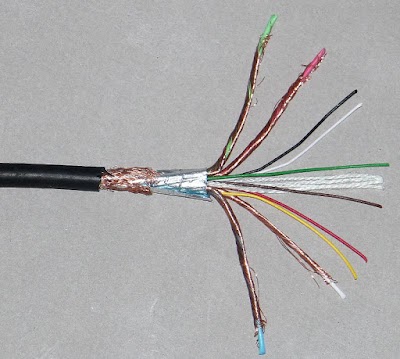
Inside a VGA cable. The cable is more complex than I expected, with multiple layers of shields. The green, red, white (sync) and blue wires are thicker and have their own shielding.

Inside a VGA cable. The cable is more complex than I expected, with multiple layers of shields. The green, red, white (sync) and blue wires are thicker and have their own shielding.

To connect to the monitor, I cut a VGA cable in half and figured out which wire goes to which pin.3 The wire (above) is constructed in an interesting way, more complicated than I expected. The red, green, blue and horizontal sync signals are transmitted over coaxial-like cables formed by wrapping a wire a spiral of thin copper wires for shielding.2 The remaining signals travel over thinner plain wires. Several strands of string form the structural center of the VGA cable, and the ten internal wires are wrapped in a foil shield and woven outer shield.

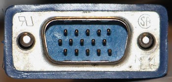
The VGA connector consists of 3 rows of 5 pins.
Pins are simply numbered left-to-right with 1 through 5 in the first row, 6-10 in the second, and 11-15 in the third.
(Click image for a closeup.)

The VGA connector consists of 3 rows of 5 pins. Pins are simply numbered left-to-right with 1 through 5 in the first row, 6-10 in the second, and 11-15 in the third. (Click image for a closeup.)

The photo above shows the male VGA connector on each end of the cable. The function assigned to each pin is shown in the table below. The I2C clock (SCL) and data (SDA) are the important pins for this project. The wire colors are not standardized; they refer to my VGA cable and may be different for a different cable.

PinFunctionWire color
1RedRed coax
2GreenGreen coax
3BlueBlue coax
4ReservedShield
5GroundBlack
6Red GroundShield
7Green GroundShield
8Blue GroundShield
95VYellow
10GroundWhite
11ReservedShield
12SDAGreen
13HSyncWhite coax
14VSyncBrown
15SCLRed

The 5 volt wire in the cable has a clever purpose. This wire allows the computer to power the EEPROM chip that provides the configuration data. Thus, the computer can query the display's characteristics even if the display is turned off or even unplugged from the wall.

Reading the configuration data

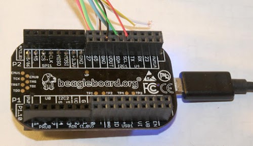
To read the data over I2C, I used the PocketBeagle, a tiny Linux computer that I had handy. (You could use a different system that supports I2C, such as the Raspberry Pi, Beaglebone or Arduino.) I simply connected the I2C clock (SCL), data (SDA) and ground wires from the VGA cable to the PocketBeagle's I2C pins as shown below.

Connecting a VGA cable to the PocketBeagle allows the configuration data to be read over I2C. The black wire is ground, the green wire is I2C data (SDA) and the red wire is I2C clock (SCL).

Connecting a VGA cable to the PocketBeagle allows the configuration data to be read over I2C. The black wire is ground, the green wire is I2C data (SDA) and the red wire is I2C clock (SCL).

Simple Linux commands let me access I2C. First, I probed the I2C bus to see what devices were present, using the i2cdetect command. (Many devices can be connected to an I2C bus, each assigned a different address.) The output below shows that devices 30, 37, 4a, 4b and 50 responded on I2C bus 1. Device 50 is the relevant I2C device, assigned to the configuration information. Device 37 is DDC/CI, allowing monitor settings to be controlled by the computer, but I'll ignore it for this post. Devices 30, 4a, and 4b are a mystery to me so leave a comment if you know what they are.

$ i2cdetect -y -r 1
     0  1  2  3  4  5  6  7  8  9  a  b  c  d  e  f
00:          -- -- -- -- -- -- -- -- -- -- -- -- --
10: -- -- -- -- -- -- -- -- -- -- -- -- -- -- -- --
20: -- -- -- -- -- -- -- -- -- -- -- -- -- -- -- --
30: 30 -- -- -- -- -- -- 37 -- -- -- -- -- -- -- --
40: -- -- -- -- -- -- -- -- -- -- 4a 4b -- -- -- --
50: 50 -- -- -- -- -- -- -- -- -- -- -- -- -- -- --
60: -- -- -- -- -- -- -- -- -- -- -- -- -- -- -- --
70: -- -- -- -- -- -- -- --

Next, I used the i2cdump command to read 128 bytes from device 50's registers, providing the raw VGA information. The hex values are on the left and ASCII is on the right.

$ i2cdump -y -r 0-127 1 0x50 b
     0  1  2  3  4  5  6  7  8  9  a  b  c  d  e  f    0123456789abcdef
00: 00 ff ff ff ff ff ff 00 04 69 fa 22 01 01 01 01    ........?i?"????
10: 12 19 01 03 1e 30 1b 78 ea 3d 25 a3 59 51 a0 25    ?????0?x?=%?YQ?%
20: 0f 50 54 bf ef 00 71 4f 81 80 81 40 95 00 a9 40    ?PT??.qO???@?.?@
30: b3 00 d1 c0 01 01 02 3a 80 18 71 38 2d 40 58 2c    ?.?????:??q8-@X,
40: 45 00 dd 0c 11 00 00 1e 00 00 00 fd 00 32 4c 1e    E.???..?...?.2L?
50: 53 11 00 0a 20 20 20 20 20 20 00 00 00 fc 00 56    S?.?      ...?.V
60: 45 32 32 38 0a 20 20 20 20 20 20 20 00 00 00 ff    E228?       ....
70: 00 46 34 4c 4d 51 53 31 32 38 35 34 36 0a 00 bb    .F4LMQS128546?.?

Understanding the monitor's EDID data

The configuration data is encoded in the EDID (Extended Display Identification Data) format, so it's not immediately obvious what the data means. But the format is well-documented, so it's not too hard to figure out. For instance, the first 8 bytes 00 ff ff ff ff ff ff 00 are the header. The next two bytes 04 69 encode three 5-bit characters for the manufacturer ID, in this case "ACI" - Asus Computer International. (The data format uses a lot of annoying bit manipulations like these to make the data compact.) Near the end of the output, the ASCII strings "VE228" and "F4LMQS128546" are clearly visible; these are the monitor's model number and serial number.

I made a simple Python program to decode the data, giving the following results:

Header:
  Manufacturer: ACI
  Product code: 8954
  Week: 18
  Year: 2008
  Edid version 1, revision 3
  Analog input
  Levels: +0.7/-.03
  Blank-to-black setup (pedestal) expected
  Separate sync supported
  Composite sync supported
  Sync on green supported
  Horizontal screen size: 48cm
  Vertical screen size: 27cm
  Display gamma: 2.200
  DPMS standby supported
  DPMS suspend supported
  DPMS active-off supported
  Display type (analog): RGB color
  Preferred timing mode in descriptor block 1
Chromaticity coordinates:  r: (0.637, 0.351), g: (0.319, 0.626), b: (0.145, 0.061), w: (0.313, 0.329)
Established timings:
  720x400 @ 70 Hz
  640x480 @ 60 Hz
  640x480 @ 67 Hz
  640x480 @ 72 Hz
  640x480 @ 75 Hz
  800x600 @ 56 Hz
  800x600 @ 60 Hz
  800x600 @ 72 Hz
  800x600 @ 75 Hz
  832x624 @ 75 Hz
  1024x768 @ 60 Hz
  1024x768 @ 72 Hz
  1024x768 @ 75 Hz
  1280x1024 @ 75 Hz
Standard timing information:
  X res: 1152, aspect 4:3, Y res (derived): 864), vertical frequency: 75
  X res: 1280, aspect 5:4, Y res (derived): 1024), vertical frequency: 60
  X res: 1280, aspect 4:3, Y res (derived): 960), vertical frequency: 60
  X res: 1440, aspect 16:10, Y res (derived): 900), vertical frequency: 60
  X res: 1600, aspect 4:3, Y res (derived): 1200), vertical frequency: 60
  X res: 1680, aspect 16:10, Y res (derived): 1050), vertical frequency: 60
  X res: 1920, aspect 16:9, Y res (derived): 1080), vertical frequency: 60
Descriptor 1: Detailed timing descriptor:
  Pixel clock: 148500kHz
  Horizontal active pixels: 1920
  Horizontal blanking pixels: 280
  Vertical active lines: 1080
  Vertical blanking lines: 45
  Horizontal front porch pixels: 88
  Horizontal sync pulse pixels: 44
  Vertical front porch lines: 4
  Vertical sync pulse lines: 5
  Horizontal image size: 477mm
  Vertical image size: 268mm
  Horizontal border pixels: 0
  Vertical border lines: 0
  Digital separate sync
  VSync serration
  Positive horizontal sync polarity
Descriptor 2: Display range limits
  Minimum vertical field rate 50Hz
  Maximum vertical field rate 76Hz
  Minimum horizontal field rate 30Hz
  Maximum horizontal field rate 83Hz
  Maximum pixel clock rate: 170Mhz
  Default GTF
Descriptor 3: Display name VE228
Descriptor 4: Display serial number F4LMQS128546

As you can see, the EDID format crams a lot of configuration information into 128 bytes. The output starts off with some basic data about the monitor's characteristics and inputs. The VGA standard doesn't nail down as many things as you'd hope. For instance the sync signals can be provided on one wire (composite), two wires (separate), or on the green wire. The output above shows my monitor supports all three sync types.

The monitor then provides a long list of supported resolutions, which is how your computer knows what the monitor supports. The "detailed timing descriptor" provides more information on signal voltage levels and timings. The timing of VGA signals contains some strange features (e.g. blanking and "front porch") inherited from obsolete CRT (Cathode Ray Tube) displays. The values in the configuration provide the information necessary for the computer's graphics board to synthesize a proper VGA signal that the monitor can understand.

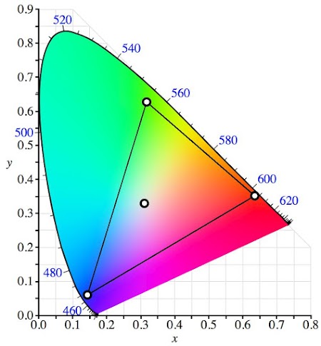
The CIE chromaticity coordinates provided by the monitor are interesting, but need a bit of background to understand. A CIE chromaticity diagram (below), shows all the colors in the real world. (Brightness is factored out, so grays and browns don't appear.) Individual wavelengths of light (i.e. the spectrum) curve around the outside of the diagram. The colors inside the curve are combinations of the pure spectral colors, with white in the middle.

CIE diagram showing the color gamut and white point of my monitor.

CIE diagram showing the color gamut and white point of my monitor.

A display, however, generates its colors by combining red, green, and blue. The result is that a display can only show the colors inside the triangle above with red, green, and blue at the corners. A display doesn't generate the light wavelengths necessary to display colors outside the triangle. Like most monitors, this monitor can only show a surprisingly small fraction of the possible colors. (A wide-gamut display uses different phosphors to expand the triangle and get more vivid colors.) The triangle vertices and white point4 in the diagram above come from the x,y chromaticity coordinates in the configuration data.

You might wonder how you can see the whole CIE diagram on your display if only the colors inside the triangle can be displayed. The answer is the diagram "cheats"—the colors are scaled to fit into RGB values, so you're not seeing the exact colors but just an approximate representation. If you look at the spectrum through a prism, for instance, the colors will be more intense than what you see in the CIE diagram.

Inside I2C

The I2C protocol (Inter-Integrated Circuit) was invented in 1982 by Philips Semiconductor to connect a CPU to peripheral chips inside televisions. It's now a popular protocol for many purposes, including connecting sensors, small LED displays, and other devices to microcontrollers. Many I2C products are available from Adafruit and Sparkfun for instance.

The I2C protocol provides a simple, medium-speed way to connect multiple devices on a bus using just two wires—one for a clock and one for data. I2C is a serial protocol, but it differs from serial protocols like RS-232 in a couple ways. First, I2C is synchronous (using a clock), unlike RS-232 which is asynchronous (no clock). Second, I2C is a bus and can connect dozens of devices, while RS-232 connects two devices.5

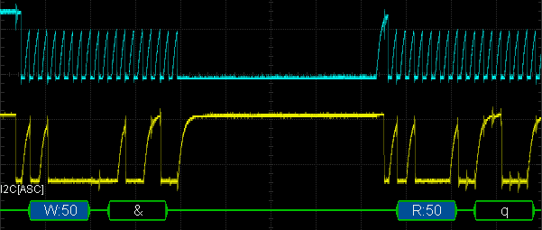
The oscilloscope trace below shows what an I2C communication with the monitor looks like on the wire. The top line (cyan) shows the clock. Note that the clock only runs while data is transmitted.) The yellow line is the binary data. At the bottom, the oscilloscope decoded the data (green). In this trace, register number 0x26 is being read from device 0x50. The I2C protocol is rather peculiar since a read is performed by doing a write followed by a read. That is, to read a byte, the master first does a write to the device of the desired register number: the master first sends 0x50 (the device ID) the write flag bit (indicated with "W:50"), and 0x26 (the register number, ASCII "&"). Then, the master does a read; it sends 0x50 and the read flag bit ("R:50"). The device responds with the value in the register, 0x71 (ASCII "q").6

I2C trace: clock (SCL) in cyan and data (SDA) in yellow. Green shows decoded data. Oscilloscope was set to 20&micro;s/division and 2V/division.

I2C trace: clock (SCL) in cyan and data (SDA) in yellow. Green shows decoded data. Oscilloscope was set to 20µs/division and 2V/division.

Devices on the I2C bus can only pull a line low; pull-up resistors keeps the lines high by default.7 As a result, the traces above drop low sharply, but climb back up slowly.8 Even though the transitions look sloppy, the I2C bus worked fine. I couldn't find a source to tell me if VGA monitors included pull-up resistors, or if I needed to add them externally. However, I measured voltage on the lines coming from the monitor and everything worked without external resistors, so there must be pull-up resistors inside the monitor.

Conclusion

The VGA specification includes a data link that allows a computer to learn about a monitor and configure it appropriately. It is straightforward to read this configuration data using the I2C protocol and a board with an I2C port. While VGA is mostly obsolete now, the same data protocol is used with DVI and HDMI displays. My goal in reading the monitor's config data was so I could use the timing data in an FPGA to generate a VGA video signal. (That project is yet to come.) Follow me on Twitter or RSS to find out about my latest blog posts.

Notes and references

  1. DDC (Display Data Channel) is used by VGA, DVI and HDMI connections, which transmit the data over two I2C pins. The data it sends is in the EDID (Extended Display Identification Data) format. Everything changed with the DisplayPort interface. It transmits configuration data over a differential AUX channel using the DisplayID format, which extends EDID to supports newer features such as 3D displays. Thus, the techniques I describe in this article should work with DVI or HDMI interfaces, but won't work with DisplayPort. 

  2. Looking at other VGA cables on the web, most VGA cables don't have the fourth coax for horizontal sync that my cable does. So my cable seems a bit unusual. 

  3. Instead of cutting a VGA cable in half, I could have simply plugged a cable into a VGA connector, but that's less interesting. 

  4. The white point for my monitor matches a standard called D65

  5. For more information on I2C, good explanations are on SparkFun and Wikipedia

  6. I'm leaving out some of the complications of I2C. For example, the master generates the clock, but the device can do "clock stretching" by holding the clock low until it is ready. Also, the device sends an ACK bit after each request. The device address is 7 bits, while the data is 8 bits. See protocol documentation for details. 

  7. Using a pull-up resistor on the I2C bus avoids the risk of short circuits. If, alternatively, devices could actively pull the line high, it would be a problem if one device tried to pull a line high at the same time another pulled it low. 

  8. The oscilloscope traces show exponential R-C charging curves when the line is pulled high. This is due to the wire capacitance being charged through the pull-up resistor. The signals only reach about 3V, making them suitable for the PocketBeagle's 3.3V inputs. (If you try this with a different monitor, check the voltage levels to avoid damaging the PocketBeagle's inputs.) 

Implementing FizzBuzz on an FPGA

I recently started FPGA programming and figured it would be fun to use an FPGA to implement the FizzBuzz algorithm. An FPGA (Field-Programmable Gate Array) is an interesting chip that you can program to implement arbitrary digital logic. This lets you build a complex digital circuit without wiring up individual gates and flip flops. It's like having a custom chip that can be anything from a logic analyzer to a microprocessor to a video generator.

The "FizzBuzz test" is to write a program that prints the numbers from 1 to 100, except multiples of 3 are replaced with the word "Fizz", multiples of 5 with "Buzz" and multiples of both with "FizzBuzz". Since FizzBuzz can be implemented in a few lines of code, it is used as a programming interview question to weed out people who can't program at all.

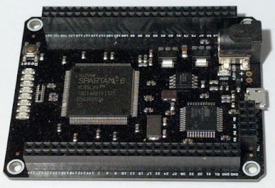
The Mojo FPGA board, connected to a serial-to-USB interface. The big chip on the Mojo is the Spartan 6 FPGA.

The Mojo FPGA board, connected to a serial-to-USB interface. The big chip on the Mojo is the Spartan 6 FPGA.

Implementing FizzBuzz in digital logic (as opposed to code) is rather pointless, but I figured it would be a good way to learn FPGAs.1 For this project, I used the Mojo V3 FPGA development board (shown above), which was designed to be an easy-to-use starter board. It uses an FPGA chip from Xilinx's Spartan 6 family. Although the Mojo's FPGA is one of the smallest Spartan 6 chips, it still contains over 9000 logic cells and 11,000 flip flops, so it can do a lot.

Implementing serial output on the FPGA

What does it mean to implement FizzBuzz on an FPGA? The general-purpose I/O pins of an FPGA could be connected to anything, so the FizzBuzz output could be displayed in many different ways such as LEDs, seven-segment displays, an LCD panel, or a VGA monitor. I decided that outputting the text over a serial line to a terminal was the closest in spirit to a "standard" FizzBuzz program. So the first step was to implement serial output on the FPGA.

The basic idea of serial communication is to send bits over a wire, one at a time. The RS-232 serial protocol is a simple protocol for serial data, invented in 1960 for connecting things like teletypes and modems. The diagram below shows how the character "F" (binary 01000110) would be sent serially over the wire. First, a start bit (low) is sent to indicate the start of a character.2 Next, the 8 bits of the character are sent in reverse order. Finally, a stop bit (high) is sent to indicate the end of the character. The line sits idle (high) between characters until another character is ready to send. For a baud rate of 9600, each bit is sent for 1/9600 of a second. With 8 data bits, no parity bit, and 1 stop bit, the protocol is known as 8N1. Many different serial protocols are in use, but 9600 8N1 is a very common one.

Serial line output of the character "F" sent at 9600 baud / 8N1.

Serial line output of the character "F" sent at 9600 baud / 8N1.

The first step in implementing this serial output was to produce the 1/9600 second intervals for each bit. This interval can be measured by counting 5208 clock pulses on the Mojo.3 I implemented this by using a 13-bit counter to repeatedly count from 0 to 5207. To keep track of which bit is being output in each interval, I used a simple state machine that advanced through the start bit, the 8 data bits, and the stop bit. The state is held in a 4-bit register. (With FPGAs, you end up dealing a lot with clock pulses, counters, and state machines.)

To create the interval and state registers in the FPGA chip, I wrote code in the Verilog hardware description language. I won't explain Verilog thoroughly, but hopefully you can get a feel for how it works. In the code below, the first lines define a 13-bit register called counter and a 4-bit register called state. The counter is incremented until it reaches 5207, at which time the counter is reset to 0 and state is incremented to process the next output bit. (Note that <= is an assignment operator, not a comparison.4) The line always @(posedge clk) indicates that the code is executed on the positive edge of each clock.

reg [12:0] counter;
reg [3:0] state;

always @(posedge clk) begin
  if (counter < 5207) begin
     counter <= counter + 1;
  end else begin
    counter <= 0;
    state <= state + 1;
  end
end

While this may look like code in a normal programming language, it operates entirely differently. In a normal language, operations usually take place sequentially as the program is executed line by line. For instance, the processor would check the value of counter. It would then add 1 to counter. But in Verilog, there's no processor and no program being executed. Instead, the code generates hardware to perform the operations. For example, an adder circuit is created to increment counter, and a separate adder to increment state, and additional logic for the comparison with 5207. Unlike the sequential processor, the FPGA does everything in parallel. For instance, the FPGA does the 5207 comparison, the increment or reset of counter and the increment of state all in parallel on each clock pulse. Because of this parallelism, FPGAs can be much faster than processors for highly parallel tasks.

The next part of the serial code (below) outputs the appropriate bit for each state. As before, while this looks like a normal programming language, it is generating hardware circuits, not operations that are executed sequentially. In this case, the code creates gate logic (essentially a multiplexer) to select the right value for out.

case (state)
  IDLE: out = MARK; // high
  START: out = SPACE; // low
  BIT0: out = char1[0];
  BIT1: out = char1[1];
  ...
  BIT6: out = char1[6];
  STOP: out = MARK;
  default: out = MARK;
endcase

There's a bit more code for the serial module to define constants, initialize the counters, and start and stop each character, but the above code should give you an idea of how Verilog works. The full serial code is here.

The FizzBuzz Algorithm

The next step is figuring out what to send over the serial line. How do we convert the numbers from 1 to 100 into ASCII characters? This is trivial when programming a microprocessor, but hard with digital logic. The problem is that converting a binary number to decimal digits requires division by 10 and 100, and division is very inconvenient to implement with gates. My solution was to use a binary-coded decimal (BCD) counter, storing each of the three digits separately. This made the counter slightly more complicated, since each digit needs to wrap at 9, but it made printing the digits easy.

I wrote a BCD counter module (source) to implement the 3-digit counter. It has three 4-bit counters digit2, digit1, and digit0. The flag increment indicates that the counter should be incremented. Usually just digit0 is incremented. But if digit0 is 9, then it wraps to 0 and digit1 is incremented. Except if digit1 is also 9, then it wraps to 0 and digit2 is incremented. Thus, the digits will count from 000 to 999.

if (increment) begin
  if (digit0 != 9) begin
    // Regular increment digit 0
    digit0 <= digit0 + 1;
  end else begin
    // Carry from digit 0
    digit0 <= 0;
    if (digit1 != 9) begin
      // Regular increment digit 1
      digit1 <= digit1 + 1;
    end else begin
      // Carry from digit 1
      digit1 <= 0;
      digit2 <= digit2 + 1;
    end
  end
end

As before, keep in mind that while this looks like normal program code, it turns into a bunch of logic gates, generating the new values for digit2, digit1 and digit0 on each clock cycle. The system isn't executing instructions in sequence, so performance isn't limited by the number of instructions but just by the delay for signals to propagate through the gates.

The next challenge was testing if the number was divisible by 3 or 5. Like division, the modulo operation is easy on a microprocessor, but hard with digital logic. There's no built-in divide operation, so modulo needs to be computed with a big pile of gates. Although the IDE can synthesize the gates for a modulo operation, it seemed inelegant. Instead, I simply kept counters for the value modulo 3 and the value modulo 5. The value modulo 3, for instance, would simply count 0, 1, 2, 0, 1, 2, ...5

The final piece of FizzBuzz was the code to output each line, character by character. In a program, we could simply call the serial output routine for each character. But in an FPGA, we need to keep track of which character is being sent, with yet another state machine. Note that to convert each digit to an ASCII character, binary 11 is concatenated, using the slightly strange syntax 2'b11. The code excerpt below is slightly simplified; the full code includes leading zero checks so "001" will print as "1".

state <= state + 1; // Different state from serial
if (mod3 == 0 && mod5 != 0) begin
  // Fizz
  case (state)
   1: char <= "F";
   2: char <= "i";
   3: char <= "z";
   4: char <= "z";
   5: char <= "\r";
   6: begin
     char <= "\n";
     state <= NEXT; // Done with output line
     end
  endcase
end else if (mod3 != 0 && mod5 == 0) begin
  ... Buzz case omitted ...
end else if (mod3 == 0 && mod5 == 0) begin      
 ... Fizzbuzz case omitted ...
end else begin 
  // No divisors; output the digits of the number.
  case (state)
    1: char <= {2'b11, digit2[3:0]};
    2: char <= {2'b11, digit1[3:0]};
    3: char <= {2'b11, digit0[3:0]};
    4: char <= "\r";
    5: begin
     char <= "\n";
     state <= NEXT;
    end
  endcase
end

Putting it all together, there are multiple state machines and counters controlling the final FizzBuzz circuit. The main state machine controls the code above, moving through the characters of the line. For each character, this state machine triggers the serial output module, and waits until the character has been output. Inside the serial module, a state machine moves through each bit of the character. This state machine waits until the baud rate counter has measured out the width of the bit. When the serial output of the character is done, the serial module signals the main state machine. The main state machine then moves to the next character in the line. When the line is done, the main state machine increments the BCD counter (counting from 1 to 100) and then starts outputting the next line.

Programming languages make it easy to do operations in sequence, perform loops, make subroutine calls and so forth. But with an FPGA, you need to explicitly control when things happen, using state machines and counters to keep track of what's happening. In exchange for this, FPGAs give you a huge degree of parallelism and control.

Running FizzBuzz on the FPGA board

To compile the Verilog code, I used Xilinx's ISE tool (below), which is a development environment that lets you write code, simulate it, and synthesize it into gate-level circuitry that can be loaded onto the FPGA. Using the ISE tool is fairly straightforward, and explained in the Mojo tutorials. The synthesis process was slow compared to a compile, taking about 45 seconds for my FizzBuzz program.

By writing Verilog code in Xilinx's ISE tool, you can program functionality into an FPGA.

By writing Verilog code in Xilinx's ISE tool, you can program functionality into an FPGA.

Once I had the code working in the simulator,7, I downloaded it to the FPGA board over a USB cable. I connected the FPGA output pin to a USB-to-serial adapter6 and used a terminal emulator (screen) to display the serial output on my computer. I hit the reset button on the Mojo board and (after just a bit more debugging) the FizzBuzz output appeared (below).

First page of output from the FizzBuzz FPGA, as displayed by the screen terminal emulator.

First page of output from the FizzBuzz FPGA, as displayed by the screen terminal emulator.

The image below shows the raw serial data from the FPGA (yellow). This is the end result of the FizzBuzz circuitry running on the FPGA board—a sequence of pulses. The oscilloscope also shows the decoded ASCII characters (green). This data is near the beginning of the FizzBuzz output, showing the lines for 2, 3 and 4. (CR and LF are carriage return and line feed.)

The serial data signal (yellow) near the beginning of the FizzBuzz output. The ASCII decoding is in green.

The serial data signal (yellow) near the beginning of the FizzBuzz output. The ASCII decoding is in green.

What happens inside the FPGA?

You might wonder how a Verilog description of a circuit gets turned into digital logic, and how the FPGA implements this logic. The ISE synthesis tool turns the Verilog design into circuitry suitable for implementation inside the FPGA. It first synthesizes the Verilog code into a "netlist", specifying the logic and connections. Next it translates the netlists into FPGA primitives, which are mapped onto the capabilities of the particular chip (the Spartan 6 in my case). Finally, the place and route process optimizes the layout of the chip, minimizing the distance signals need to travel.

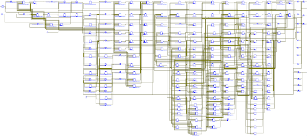
Schematic of the FizzBuzz circuit.

Schematic of the FizzBuzz circuit.

The image above shows the schematic of the FizzBuzz circuit, as generated by the synthesis tools. As you can see, the Verilog code turns into a large tangle of circuitry. Each block is a flip flop, logic element, multiplexer or other unit. These blocks make up the counters, state registers and logic for the FizzBuzz circuit. While this looks like a lot of logic, it used less than 2% of the chip's capability. A closeup (below) of the schematic shows a flip flop (labeled "fdre")8 and a lookup table (labeled "lut5") from the BCD counter. The nice thing about Verilog is that you can design the circuit at a high level, and it gets turned into the low-level circuitry. This is called RTL (Register-transfer level) and lets you design using registers and high-level operations on them, without worrying about the low-level hardware implementation. For instance, you can simply say count + 1 and this will generate the necessary binary adder circuitry.

Detail of the schematic showing a flip flop and lookup table.

Detail of the schematic showing a flip flop and lookup table.

The FPGA chip uses an interesting technique to implement logic equations. Instead of wiring together individual gates, the logic is implemented with a lookup table (LUT), which is a flexible way of implementing arbitrary logic. Each lookup table has 6 input lines, so it can implement any combinatorial logic with 6 inputs. With 6 inputs, there are 64 different input combinations, yielding a 64-line truth table. By storing this table as a 64-bit bitmap, the LUT can implement any desired logic function.

For example, part of the logic for the output pin is equivalent to the logic circuit below. This is implemented by storing the 64-bit value FFFFA8FFFFA8A8A8 into the lookup table. In the Spartan 6 chip, the LUT is implemented with 64 bits of static RAM, loaded when the FPGA is initialized. Since the chip has 5720 separate lookup tables, it can be programmed to implement a lot of arbitrary logic.

The gate logic implemented by one lookup table in the FPGA.

The gate logic implemented by one lookup table in the FPGA.

The final piece of the FPGA puzzle is the switch matrix that connects the circuitry together in arbitrary ways. In the Spartan 6 a handful of LUTs, flip flops and multiplexers are grouped into a configurable logic blocks (CLB).9 The CLBs are connected together by a switch matrix, as shown below. Each switch matrix block is programmed to connect different wires together, allowing the FPGA to be wired as desired. An important part of the FPGA synthesis process is positioning blocks to minimize the wiring distance, both to minimize signal propagation delay and to avoid running out of interconnect paths.

The switching matrix in the Spartan 6 FPGA allows arbitrary interconnections between CLBs. From the User Guide.

The switching matrix in the Spartan 6 FPGA allows arbitrary interconnections between CLBs. From the User Guide.

Should you try an FPGA?

Personally, I was very reluctant to try out an FPGA because they seemed scary and weird. While there is a learning curve, FPGAs aren't as difficult as I expected. If you're interested in new programming paradigms, FPGAs will definitely give you a different perspective. Things that you take for granted, such as performing operations in sequence, will move to the foreground with an FPGA. You can experiment with high degrees of parallelism. And FPGAs will give you a better idea of how digital circuits work.

However, I wouldn't recommend trying FPGAs unless you have some familiarity with wiring up LEDs and switches and understand basic digital logic: gates, flip flops, and state machines. If you're comfortable with an Arduino, though, an FPGA is a reasonable next step.

For most applications, a microcontroller can probably do the job as well as an FPGA and is easier to program. Unless you have high data rates or require parallelism, an FPGA is probably overkill. In my case, I found a microcontroller was barely powerful enough for my 3Mb/s Ethernet gateway project, so I'm looking into FPGAs for my next project.

Is the Mojo a good board to start with?

The Mojo FPGA development board is sold by Adafruit and Sparkfun, so I figured it would be a good hacker choice. The Mojo was designed for people getting started with FPGAs, and I found it worked well in this role. The makers of the Mojo wrote a solid collection of tutorials using Verilog.10 It was very helpful to use tutorials written for the specific board, since it minimized that amount of time I spent fighting with the board and tools. The Mojo is programmed over a standard USB cable, which is more convenient than boards that need special JTAG adapters.

The Mojo FPGA board. The Spartan-6 FPGA chip dominates the board.

The Mojo FPGA board. The Spartan-6 FPGA chip dominates the board.

Although the Mojo has plenty of I/O pins, it doesn't have any I/O devices included except 8 LEDs. It would be nicer to experiment with a board that includes buttons, 7-segment displays, VGA output, sensors and so forth. (It's not hard to wire up stuff to the Mojo, but it would be convenient to have them included.) Also, some development boards include external RAM but the Mojo doesn't, a problem for applications such as a logic analyzer that require a lot of storage.11 (You can extend the Mojo with an IO shield or RAM shield.)

A good introductory book to get started with the Mojo is Programming FPGAs; it also covers the considerably cheaper Papilo One and Elbert 2 boards. A list of FPGA development boards is here if you want to look at other options.

Conclusion

An FPGA is an impractical way to implement FizzBuzz, but it was a fun project and I learned a lot about FPGA programming. I certainly wouldn't get the FPGA job if FizzBuzz was used as an interview question, though! My code is on github, but keep in mind I'm a beginner to FPGAs.

Follow me on Twitter or RSS to find out about my latest blog posts.

Notes and references

  1. It's trivial to implement a microprocessor on an FPGA. For instance, with the Spartan 6 chip you can click a couple buttons in an IDE wizard and it will generate the circuitry for a MicroBlaze processor. Thus, the sensible way to run FizzBuzz on an FPGA would be to write the FizzBuzz code in a few lines of C, and then run it on a processor inside the FPGA. But that's too easy for me. 

  2. The start bit is necessary because otherwise the receiver couldn't tell when the character started, if the first bit sent was a 1. 

  3. Since the Mojo uses a 50 MHz clock, for 9600 baud each output bit is 50,000,000 / 9600 or approximately 5208 clocks wide. 9600 baud isn't a very fast rate so to challenge my circuit, I also tested it at 10M baud (by counting to 5 for each bit) and the circuit worked fine. (The USB-to-serial interface only worked up to 230400 baud, so I used oscilloscope decoding to check the higher speeds.) 

  4. In Verilog, <= is the nonblocking assignment operator, while = is the blocking assignment operator. Nonblocking assignments happen in parallel, and are generally used for sequential (clocked flip flop) logic. Blocking assignment is used for combinational (nonclocked) logic. This is a bit confusing but details are here

  5. I used BCD and not binary to store the number, so computing the value modulo 5 would have been almost trivial by looking at the last digit. But modulo 3 would still be difficult, so I stuck with the counter approach. 

  6. I couldn't connect the serial input directly to my computer, since it doesn't have a serial port. Instead, I used a USB-to-serial adapter, Adafruit's FTDI Friend. This adapter also had the advantage of accepting the FPGA's 3.3V signals, rather than the inconvenient +/- 15V used by genuine RS-232. 

  7. Debugging an FPGA is a very different process from software debugging. Since the FPGA is mostly a black box while running, you should test everything out in the simulator first, or else you end up in "FPGA Hell", blinking LEDs to figure out what's happening. To debug code, you simulate it by writing a "testbench", Verilog code that specifies various inputs at various times (example). You then run the simulator (below) and examine the output to make sure it is correct.

    The ISim simulator from Xilinx allows an FPGA design to be simulated.

    The ISim simulator from Xilinx allows an FPGA design to be simulated.

    If things go wrong, the simulator lets you step through the internal signals to find the problem. After testing everything in the simulator, my code only had trivial problems when I tried it on the real FPGA. My main problem was I assigned the serial output to the wrong pin on the board, so there was no output. 

  8. The Spartan 6 FPGA supports multiple types of flip flop. The FDRE is a D-Flip flop with synchronous Reset and clock Enable. 

  9. The Spartan 6 FPGA's configurable logic blocks (CLBs) are moderately complex, combining LUTs, 8 flip flops, wide multiplexers, carry logic, distributed RAM and shift registers. Hard-wiring components into the these blocks reduces flexibility slightly, but makes the switch matrix much simpler. The CLBs are described in detail in the CLB User Guide. The Spartan 6 FPGA also contains other types of blocks such as clock generation blocks and DSP blocks that can do fast 18-bit multiplication. 

  10. An alternative to the Verilog language is VHDL, which is also supported by the development environment. The Mojo also supports Lucid, a simpler FPGA language developed by the Mojo team. The Mojo Lucid tutorials explain the language, and there is a book available on Lucid. I decided I'd rather learn a standard language rather than Lucid though. 

  11. Although the Mojo doesn't have external RAM, its FPGA has 576 kilobits of internal RAM. This is tiny compared to boards with megabytes of external DRAM, though.