A few days ago, I wrote about how I'm helping restore a Xerox Alto for Y Combinator.
This new post describes the first day of restoration: how we disassembled the computer and disk drive and fixed a power supply problem, but ran into a showstopper problem with the disk interface.
The Xerox Alto was a revolutionary computer from 1973, designed by computer pioneer Chuck Thacker at Xerox PARC
to investigate ideas for personal computing.
The Alto was the first computer built around a mouse and GUI, as well as introducing Ethernet and laser printers to the world.
The Alto famously inspired Steve Jobs, who used many of its ideas in the Lisa and Macintosh computer.
Alan Kay, whose vision for a personal computer guided the Alto, recently gave an Alto computer to Y Combinator.
Getting this system running again is a big effort but fortunately I'm working with a strong team, largely from the IBM 1401 restoration team. Marc Verdiell, Luca Severini, Ron, Carl Claunch, and I started on restoration a few days ago, as shown in Marc's video below.
Disassembling the Alto
We started by disassembling the computer.
The Xerox Alto has a metal cabinet about the size of a dorm mini-fridge, with a Diablo hard disk drive on top, and a chassis with power supplies and the circuit boards below. With some tugging, the chassis slides out of the cabinet on rails as you can see in the photo below. At the front are the four cooling fans, normally protected by a decorative panel.
Note the unusual portrait layout of the display.
The Xerox Alto II XM 'personal computer'. The card cage below the disk drive has been partially removed. Four cooling fans are visible at the front of it.
With the chassis fully removed, you can see the four switching power supplies on the left, the blue metal boxes. The computer's circuit boards are on the right, not visible in this picture.
The wiring for the backplane is visible at right front, with pins connected by wire-wrapped wire connections. This wiring connects the circuit boards together.[1]
The Alto's chassis has been removed. On the left are the four switching power supplies (blue boxes). On the right, the connections for the wire-wrapped backplane are visible. The circuit boards plug into this backplane.
The power supplies
Our first goal was to make sure the power supplies worked after decades of sitting idle.
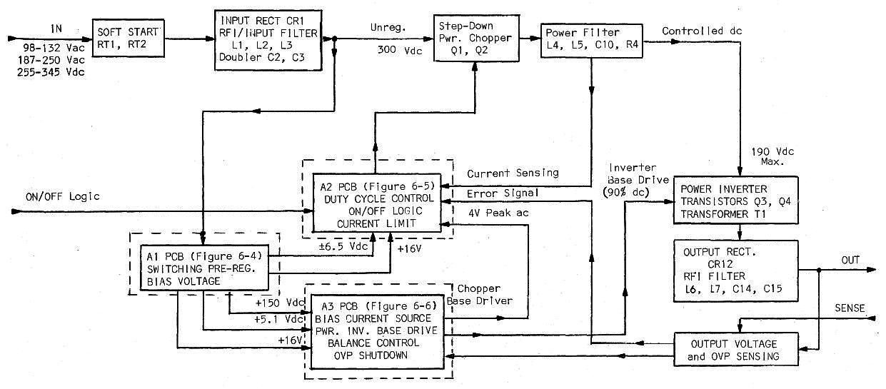
The Alto uses high-efficiency switching power supplies.[2]
To explain the power supplies in brief, input power is chopped up thousands of times a second to produce a regulated voltage. Unlike modern computer power supplies, there's a second switching stage (the inverter), which drops the voltage to the desired 15 volts.
This was more complexity than I expected, but
fortunately the detailed power supply manual was available online, thanks to Al Kossow's bitsavers.[3]
We tested each power supply with a resistor as a dummy load and checked that the output voltage was correct. We also used an oscilloscope to make sure the output was stable.
All the power supplies worked fine, except for the +15V supply (top center), which had trouble getting up to 15 volts and staying there.
We disassembled the faulty power supply to track down the problem.
The photo of the power supply below shows how densely components are crammed into the power supply. Two of the circuit boards have been removed and are at the back. Note the three large filter capacitors at the front.
Switching power supply from the Xerox Alto computer. Two of the control boards have been removed and are visible at back.
We noted signs of overheating on the AC connector, as well as a somewhat sketchy looking repair (a trace replaced by a wire) and some signs of corrosion. Apparently the power supply had problems in the past and had been serviced. We cleaned up the corrosion and it appeared to be superficial.
The power supply disassembled easily for repair, as you can see below.
The main board is at the right.
The tower of three inductors on the main board is an unusual way of mounting inductors.
Three circuit boards (top) plug into the main board. Because the power supply uses discrete components instead of a modern SMPS control IC, it needs a lot of control circuitry.
The switching transistors (lower center) are mounted onto metal heat sinks for cooling.
The Alto's switching power supply, disassembled. The main board is in the lower right. The three circuit boards are at top, below the large input capacitors.
The large capacitors were attached with screws, making it easy to remove them for testing.
A capacitance meter showed that the three large capacitors had failed, explaining why the power supply had trouble outputting the desired voltage.
Ron went off and found replacement capacitors, although they weren't an exact match for the originals. With the new capacitors mounted in place, the power supply worked properly.
Inside the Diablo disk drive
We also looked at the Diablo disk drive, which provides 2.5MB of storage for the Xerox Alto. The first step was removing the disk pack.
In normal operation, the front of the drive is locked shut to keep the disk from being removed during use.
To remove the disk without powering up the drive, we had to open the drive and manually trip the latch that locks it shut (see
Diablo drive manual).
This picture shows the disk pack being reinserted into the drive.
Unlike modern hard disk drives, the Alto's disk can be removed from the drive.
Users typically used different disks for different tasks — a programming disk, a word processing disk, and so forth.
The disk pack is a fairly large white package, resembling a cross between an overgrown Frisbee and a poorly-detailed Star Wars spaceship.
The drive's multiple circuit boards are also visible in the photo.[4]
Inserting a 2.5 MB hard disk pack into the Diablo drive used by the Xerox Alto computer.
As the disk pack enters the drive, it opens up to provide access to the disk surface.
The photo below shows the exposed surface of the disk, brownish from the magnetizable iron oxide layer over the aluminum platter.
The read/write head is visible above the disk's surface, with another head below the disk. The disk stores data in 203 concentric pairs of tracks, with the heads moving in and out together to access each pair of tracks.
Closeup of the hard disk inside the Diablo drive. The read/write head (metal/yellow) is visible above the disk surface (brown).
Although the heads are widely separated during disk pack insertion, they move very close to the disk surface during operation,
floating about one thousandth of a millimeter above the surface.
The diagram below from the manual helps visualize this minute distance, and illustrates the danger of particles on the disk's surface.
The Diablo disk and why contaminants are bad, from the Alto disk manual.
The disk interface cliffhanger
The final activity of the day was making sure all the Alto's circuit boards were in the right slots and the cables were all hooked up properly.[5]
Everything went smoothly until I tried to hook up the Diablo disk drive to the disk interface card: the disk drive cable didn't fit on the card's connector!
The cable to the Alto disk didn't fit onto the disk interface card!
After trying various combinations of cables and edge connectors,
we discovered that the rainbow-colored ribbon cable you can see in the lower right above did fit the disk interface card. But instead of going to the Diablo disk drive, this cable went to a connector on the back of the Alto labeled "Tricon".
Tricon is the controller for the Trident Disk, a high-capacity disk drive that could be used with the Alto, providing 80 MB instead of the just 2.5 MB that the standard Diablo drive provides.
Looking at the disk interface card more closely, we saw it was labeled "Alto II Trident Disk Interface" (upper left corner of the photo below), confirming that it was for the Trident.
Trident Disk Interface card for Xerox Alto computer. (See label in upper left.)
It was a shock to discover the disk interface card was for the Trident drive, since our Alto has
the standard Diablo drive, which is completely incompatible with the Trident.[6]
We checked all the boards and verified that the system was missing the Diablo interface board.
This was a showstopper problem; with the wrong board, the disk drive would be unusable and we wouldn't be able to boot up the system.
What could we do? Network boot the Alto? Build a disk simulator? Find a Trident drive on eBay? (We actually found a Trident disk platter on eBay for $129, but no drive.)
Tune in next episode to find out what we did about the disk interface problem. (Spoiler: we found a solution thanks to Al Kossow.)
Notes and references
[1]
The physical layout of the power supplies is specified on page 11 of
the Alto documentation introduction.
On the top are three Raytheon/Sorensen power supplies, +12V (15A), +15V (12A), and -15V (12A).
At the bottom is a large LH Research Mighty Mite power supply providing +5V (60A) and -5V (12A).
Why the variety of voltages? Most of the circuitry in the Alto uses 5V, which is standard for TTL chips.
The MOS memory chips use +5V, -5V and +12V. The Ethernet card uses +15V and -15V, with +15V powering the transceiver. The disk drive uses +/- 15V.
[2]
Steve Jobs claimed that the Apple II's use of a switching power supply was a revolutionary idea
ripped off by other computer manufacturers. However, the Alto is just one of many computers that used switching
power supplies before Apple (details).
[3]
For full details on the power supply operation, see the
block diagram.
First, the 115V AC line input is converted to 300V DC by a rectifier and voltage doubler. (The voltage doubler is a clever way of supporting both 115V and 230V inputs; using the doubler with 115V. This is why older PCs have a switch on the power supply to select 115V or 230V. Modern power supplies handle a wide input range, and don't require a switch.)
Next, the power supply has a chopper, a PWM transistor circuit that chops up the 300V DC, producing a regulated 120V-200V DC, depending on the output load. This goes to the inverter, which drives a step-down/isolation transformer that produces the desired 15V output. A regulation circuit sends feedback to the chopper based on the output voltage. Meanwhile, an entirely separate switching power supply circuit generates voltages (including +150V) used by the power supply internally.
Modern power supplies use a single switching stage in place of the separate chopper and inverter. I believe the two stages were used to reduce the load on the bipolar switching transistors, which don't have the performance of modern MOSFET switching transistors. (As Ron pointed out, modern power supplies often have a PFC (power factor correction) stage for improved efficiency. Thus, the two-stage design has returned, although the stages are entirely different now.)
Modern power supplies use a power supply control IC. The Alto's power supply instead has control circuits built from simple components: transistors, op amps, 555 timers.
This is one reason the power supply requires three circuit boards.
[4]
The following table from the Alto disk manual gives the stats for the drive.
Statistics on the Diablo 31 disk used with the Xerox Alto computer.
[5]
The Alto backplane has 21 slots, not all of which are used in our system.
The list of which board goes into which slot is on page 8 of
the Alto documentation.
[6]
I suspect that the Y Combinator Alto originally had both a Trident drive and a Diablo drive (as well as four Orbit boards to drive a laser printer), and when it was taken out of service, the Trident drive, the Diablo interface board, and the Orbit boards went off somewhere else.
This left the Alto with a drive that didn't match the interface card.
For reference, schematics and documentation on the Trident interface board are here.
Despite all the chips on the disk interface board, it doesn't do very much, since each TTL chip is fairly simple.
The interface board has some counters, one word data buffers, parallel/serial conversion, and a bit of control logic.
The Alto was designed to offload many hardware tasks to microcode, so the hard work of disk I/O is performed in microcode (software).
Alan Kay recently gave his 1970's Xerox Alto to Y Combinator and I'm helping with the restoration
of this legendary system.
The Alto was the first computer designed around a graphical user interface
and introduced Ethernet and the laser printer[1]
to the world.
The Alto also was one of the first object-oriented systems, supporting the Mesa and Smalltalk languages.
The Alto was truly revolutionary when it came out in 1973, designed by computer pioneer Chuck Thacker.
Xerox built about 2000 Altos for use in Xerox, universities and research labs, but the Alto was never sold as a product.
Xerox used the ideas from the Alto in
the Xerox Star, which was expensive and only moderately successful.
The biggest impact of the Alto was in 1979 when Steve Jobs famously toured Xerox and saw the Alto and other machines.
When Jobs saw the advanced graphics of the Alto, he was inspired to base the user interfaces of the Lisa and Macintosh systems on Xerox's ideas, making the GUI available to the mass market.[2]
How did Y Combinator end up with a Xerox Alto? Sam Altman, president of Y Combinator has a strong interest in the Alto and its place in computer history. When he mentioned to Alan Kay that it would be fun to see one running, Alan gave him one.
This article gives an overview of the Alto, its impact, and how it was implemented.
Later articles will discuss the restoration process as we fix components that have broken over the decades and get the system running.
The Xerox Alto II XM computer. Note the video screen is arranged in portrait mode. Next to the keyboard is a mouse. The Diablo disk drive is below the keyboard. The base contains the circuit boards and power supplies.
The photo above shows Y Combinator's Alto computer.
The Alto has an unusual portrait-format display, intended to match an 8½" by 11" page of paper.
Most displays of the time were character-oriented, but the Alto had a bitmapped display, with each of the 606x808 pixels controllable independently. This provided unprecedented flexibility for the display and allowed WYSIWYG (what-you-see-is-what-you-get) editing.
The bitmapped display memory used almost half the memory of the original Alto, however
In front of the keyboard is the three-button mouse.
Xerox made the mouse a fundamental input device for the Alto and designed the user interface around the mouse.
The disk drive at the top of the cabinet takes a removable 2.5 megabyte disk cartridge. The small capacity of the disk was a problem for users, but files could also be accessed over the Ethernet from file servers.
The lower part of the cabinet contains the computer's circuit boards and power supplies, which will be discussed below.
Dynabook and the vision of the Alto
The motivation for the Alto was Alan Kay's Dynabook project.
In 1972, he wrote A Personal Computer for Children of All Ages, setting out his vision for a personal, portable computer for education (or business), with access to the world's knowledge.
In effect, Alan Kay presented a detailed vision for the touchscreen tablet decades before
it was practical.[3]
Alan Kay with a mockup of the Dynabook.
Although the Dynabook was proposed years before the necessary hardware was available, the ideas could be tried out on the Alto, an "interim Dynabook".
Photo by Marcin Wichary, CC BY 2.0.
The Dynabook (seen in mockup above) was to be a low-cost, battery-powered, portable computer with a touchscreen and graphics, able to access information over the network. The system would be highly interactive and programmable in an object-oriented language. As well as the keyboard, voice input could be used. Books could be downloaded and purchased.
Since the necessary hardware was science fiction when the Dynabook was proposed, the Alto was built as an "interim Dynabook" for research.
Butler Lampson's 1972 memo entitled "Why Alto" proposed using the Alto for research in distributed computing, office computing, graphics, and personal computing. He stated,
"If our theories about the utility of cheap,
powerful personal computers are correct, we should be able to demonstrate
them convincingly on Alto."
Xerox used the Alto to research and develop the ideas of personal computing.[4]
Software
The Alto had a large collection of software, largely implemented in the BCPL (predecessor to C), Mesa and Smalltalk languages.
The Bravo text editor (seen below) is considered the first WYSIWYG editor, with formatted text on the screen matching the laser printer output.
Also below is the Draw illustration program which used the mouse and an icon menu to create drawings.
Other significant programs included email, file transfer (FTP) and an integrated circuit editor.
The Alto also ran some of the first networked multiplayer games such as Alto Trek and Maze War.
Bravo was the word processor for the Xerox Alto, providing WYSIWYG text editing.
The Draw program for the Xerox Alto uses the mouse and icons for drawing.
The Alto simulator Salto was used for these images.
Hardware
The Alto was introduced in 1973.
To understand this time in computer hardware, the primitive 4004 microprocessor had been introduced a couple years earlier.
Practical microprocessors such as the 6502 and Z-80 were still a couple years in the future and the Apple II wouldn't be released until 1977.
At the time, minicomputers such as the Data General Nova and PDP-11 built processors out of hundreds of simple but fast TTL
integrated circuits, rather than using slow, unreliable MOS chips.
The Alto was built similarly, and is a minicomputer, not a microcomputer.[5]
The Alto has 13 circuit boards, crammed full of chips.
Each board is a bit smaller than a page of paper, about 7-5/16" by 10", and holds roughly 100 chips (depending on the board).
For the most part, the chips are bipolar TTL chips in the popular 7400 series.
(The MOS memory chips are an exception.)
The image below shows the Alto's card rack and some of the boards.
The Xerox Alto contains 21 slots for circuit boards. Each board is crammed with chips, mostly TTL.
The Alto's CPU consists of three boards.
The Control board is the heart of the processor: it manages the 16 microcode tasks and contains microcode in PROM.
The ALU board performs arithmetic and logic operations, and provides the main register storage.
The Control RAM board provides additional microcode storage in RAM and additional processor registers.
(Note that in a few years, a single chip microprocessor could replace these three boards.)
The photo below shows the ALU board. The 16-bit addition, subtraction and Boolean operations are performed by four of the popular 74181 ALU chip, used in many other processors of the era.
Each 16-bit register requires multiple chips for storage.
The 32x16 register file is historically interesting as it is built from i3101 64-bit bipolar memory chips, Intel's first-ever product.
The ALU board from the Xerox Alto.
The Alto came out at a time when memory was expensive and somewhat unreliable.[6]
In 1970, Intel introduced the first commercially available DRAM memory, the 1103 chip, holding 1 kilobit of storage and making
magnetic core memory obsolete.
The original Alto used 16 boards crammed full of these chips to provide 128 kilobytes of memory.
The Alto we have is a more modern Alto II XM (eXtended Memory) with 512 kilobytes of storage on four boards.
Even so, the limited memory capacity was a difficulty for programmers and users.
The photo below shows one of the memory board, packed with denser 16 kilobit chips.
A 128KB memory card from the Xerox Alto. It uses eighty 4116 memory chips, each with 16 kilobits of storage.
Microcode
The Alto hardware provides a simple micro-instruction set and uses
microcode to implement a full instruction set on top of this,[7]
including some very complex instructions.
The Alto introduced the
BITBLT graphics instruction, which draws an arbitrary bitmap to the display in a variety of ways (e.g. paint over, gray stipple or XOR).
"Blitting" became a standard graphics operation, still be found in Windows.
The Alto takes microcode further than most computers,
implementing many functions in microcode that most computers implement in hardware, making the Alto hardware simpler and more flexible.[8]
Microcode tasks copy every pixel to the display 30 times a second, refresh dynamic memory, read the mouse, handle disk operations, drive Ethernet — operations performed in hardware on most computers.
Much of the Alto microcode is stored in RAM, so languages or even user programs can run custom microcode.
Next steps
The first step to getting the system running will be to make sure the power supplies work and provide the proper voltages.
The Alto uses four complex but highly efficient switching power supplies: +15V, -15V, +12V, and +/-5V.[9]
(Most of the chips use +5V, but the memory chips and some interfaces require unusual voltages.)
The power supplies are mounted in the cabinet behind the card cage, as you can see in the photo below. The +/-5V supply is on the right, and the three other power supplies are on the left.
Looking into the back of the Alto, you can see the four switching power supplies (blue). The card cage is behind them. The disk drive has been removed from the top of the cabinet. On the back of the cabinet, connectors to the display, Ethernet, and other devices are visible.
Restoring this systems is a big effort but fortunately there's a strong team working on it, largely from the IBM 1401 restoration team. The main Alto restorers so far are Marc Verdiell, Luca Severini, Ron, and Carl Claunch. Major technical contributions have been provided by Al Kossow (who has done extensive Alto restoration work in the past and is at the Computer History Museum) and the two Keiths (who have restored Altos at the Living Computer Museum).
For updates on the restoration, follow kenshirriff on Twitter.[10]
Notes and references
[1]
The laser printer was invented at Xerox by Gary Starkweather and networked laser printers were soon in use with the Alto. Y Combinator's Alto is an "Orbit" model, with slots for the four boards that drive the laser printer, laboriously rendering 16 rows of pixels at a time.
[2]
Malcolm Gladwell describes Steve Jobs' visit to Xerox in detail in Creation Myth.
The article claims that Xerox licensed its technology to Apple, but strangely
that license wasn't mentioned in
earlier articles about Xerox's lawsuit against Apple.
The facts here seem murky.
[3]
Amazingly, Alan Kay even predicted ad blockers in his 1972 Dynabook paper:
"One can imagine one of the first programs an owner will write is a filter to eliminate advertising!"
I thought that Alan Kay missed WiFi in the Dynabook design, but as he points out in the comments, wireless networking was a Dynabook feature.
[4]
Xerox called the Alto "a small personal computing system", saying,
"By 'personal computer' we mean a non-shared system containing sufficient
processing power, storage, and input-output capability to satisfy the computational needs of a single user." (See ALTO: A Personal Computer System Hardware Manual.) Xerox's vision of personal computing is described in the retrospective Alto: A personal computer.
[5]
The Alto documentation refers to the microprocessor, but this
term describes the microcode processor.
The Alto does not use a microprocessor in the modern sense.
[6]
Since memory chips of the era were somewhat unreliable (especially in large quantities),
the Alto used parity plus 6 bits of error correcting code to improve reliability.
As well as the four memory boards, the Alto has three memory control boards to decode addresses and implement error correction.
[7]
The Alto's microcode instructions and "real" instructions (called Emulated Instructions) are
described in the Hardware Reference.
The Alto's instruction set is similar to the Data General Nova.
[8]
The Alto has 16 separate microcode tasks, scheduled based on their priority.
The Alto's microcode tasks are described in Appendix D of the Hardware Manual.
The display task illustrates how low-level the microcode tasks are.
In a "normal" computer, the display control hardware fetches pixels from memory.
In the Alto, the display task in microcode copies pixels from memory to the display hardware's 16 word pixel buffer as each line is being written to the display. The point is that the hardware is simplified, but the microcode task is working very hard, copying every pixel to the display 30 times a second.
Similarly the Ethernet hardware is simplified, since the microcode task does much of the work.
[9]
Steve Jobs claimed that the Apple II's use of a switching power supply was a revolutionary idea
ripped off by other computer manufacturers. However, the Alto is just one of many computers that used switching
power supplies before Apple (details).
[10]
Many sources have additional information on the Alto.
Bitsavers has a large collection of Alto documentation.
DigiBarn has photos and more information on the Alto.
The Computer History Museum has a large collection of Alto source code online here.
The Alto simulator Salto is available here if you want to try out the Alto experience.
Wikipedia has a detailed article on the Alto.
Punched card sorters were a key part of data processing from 1890 until the 1970s, used for
accounting, inventory, payroll and many other tasks.
This article looks inside sorters, showing the fascinating electromechanical and vacuum tube circuits used for data processing in the pre-computer era and beyond.
Herman Hollerith invented punch-card data processing for the 1890 US census.[1]
Businesses soon took advantage of punched cards for data processing, using what was called
unit record equipment.
Each punched card held one data record, consisting of multiple data fields.
A card sorter sorted the cards into the desired order. Then a machine called a tabulator read the cards, added up desired fields and printed a report.
For example, a company could have one card for each invoice it needs to pay, as shown below, with fields for the vendor number, date, amount to pay, and so forth.
The card sorter ordered the cards by vendor number.
Then the tabulator generated a report by reading each card and printing a line for each card.
Mechanical counters in the tabulator summed up the amounts, computing the total amount payable.
Many other business tasks such as payroll, inventory and billing used punched cards in a similar manner.
Example of a punched card holding a 'unit record', and a report generated from these cards. From Functional Wiring Principles.
The surprising thing about unit record equipment is that it originally was entirely electro-mechanical, not even using vacuum tubes.
This equipment was built from components such as wire brushes to read the holes in punched cards, electro-mechanical relays to control the circuits, and mechanical wheels to add values.
Even though these systems were technologically primitive, they revolutionized business data processing and paved the way for electronic business computers such as the IBM 1401.
How a sorter works
A card sorter takes punched cards and sorts them into order based on a field, for example employee number, date, or department.
One application is putting records in the desired order when printing out a report.[2]
Another application is grouping record by a field, for instance to generate a report of sales by department:
the cards are first sorted based on the department field, and then a tabulator sums up the sales field, printing the subtotal for each department.
To sort punched cards, they are loaded into the card hopper and fed through the sorter. Cards are read and directed into one of the 13 card pockets: 0 through 9, two "zone" pockets, and a Reject pocket.
This is very different from a typical sort algorithm — cards aren't compared with each other — so you may wonder how this machine sorts its input.
IBM Type 80 Card Sorter.
Card sorting uses a clever technique called
radix sort.
The sorter operates on one digit of the field at a time, so to sort on a 3-digit field, cards are run through the sorter three times.
First, the sorter deposits the cards into ten bins (0-9) based on the lowest digit of the field.
The operator gathers up the cards from the bins in order (0 bin first and 9 bin last) and they are sorted again on the second-lowest digit, again getting stacked in bins 0-9.
The important thing is that the cards in each bin will still be ordered from the first pass: bin 0 will have cards ending in 00 first, and cards ending in 09 last.
The operator gathers up the cards in order again, yielding a stack that is now sorted according to the last two digits.
The cards are run through the sorter a third time, this time sorting on the third-lowest digit.
After the last run through the sorter, the cards are in order, sorted on the entire field.
The radix sort process is fast and simple. You may be familiar with comparison-based sorting algorithms like quicksort that compare and shuffle entries, taking O(n log n) time. Radix sort can be implemented with a simple electric mechanism (along with an operator busily moving stacks of cards around), and takes linear time.[3]
Although the sorter's hopper can hold 3600 cards, it can sort as many cards as desired, as long as the operator keeps loading and unloading them.
The sorting mechanism
You might expect a sorter to have multiple sensors to read the holes from a card and 10 flippers to direct the card into the right bin. But the actual implementation of the early sorters is amazingly simple and clever, using a single sensor and a single electromagnet.
An IBM punched card, showing the encoding of digits and letters.
The photo above shows the layout of a standard IBM punched card, which stores
80 characters in 80 columns. The characters are printed along the top of the card and the corresponding holes are punched below.
For a digit, each column has a single punch in row 0 through 9 to indicate the digit in that column.
(I'll explain the two additional "zone" rows for alphabetic characters later.)
The diagram below shows how the card sorter works.
Cards are fed through the sorter "sideways" starting with the bottom edge (called the "9-edge" because the bottom row is row 9).
A small wire brush (red) detects the presence or absence of a hole; the brush will contact the rows in order from 9 to 0. An intact card blocks the wire brush from contacting the metal roller. But if there is a hole in the card, the brush makes contact with the roller through the hole, completing an electrical circuit.
Card sorting mechanism in the IBM Type 80 and Type 82 card sorter.
A stack of metal guides (called chute blades) is used to direct the card into the appropriate bin.
As a card is fed through the sorter mechanism, it slides under the chute blades as shown in the top illustration.
If the brush (red) makes contact through a hole, it trips an electromagnet (purple) that pulls down a metal armature plate (green), allowing the ends of the chute blades to drop down.
This causes the card to go above the chute blade rather than underneath it.
The key is the chute blades have the same spacing as the rows on the card
so the hole is detected just before the card reaches the corresponding blade.
(If no hole is detected, the card passes under all the chute blades and into the Reject bin.)
For example, in the diagram above the card has slid under chute blades 9 through 5.
The brush makes contact through hole 4, energizing the electromagnet and causing the blades to drop
just before the card reaches blade 4. Thus, the card is directed into chute 4.
The chute blades can be seen in the photo below; they are the metal strips running down the center of the sorter between the feed rollers. Each chute blade ends at the appropriate pocket, causing the card to drop into the right location.
IBM Type 82 Card Sorter. The feed rollers under the glass top send cards through the sorter. The pockets at bottom collect the cards. This is a German model, thus the 'Sorteirmaschine' label.
Alphabetic sorting
Numeric values have one hole in a column and are straightforward to sort, but how about alphabetic characters?
In addition to the ten numeric rows 0-9, punched cards also have two additional "zone" rows (11 and 12).
The diagram below shows the encoding; a letter combines
a digit punch (1-9) with a zone punch (a hole in 0, 11 or 12).
Confusingly, row 0 is used both as a zone and a digit.
The IBM punched card code, from IBM 82, 83, and 84 Sorters Reference Manual.
With this encoding, a sorter can perform an alphabetical sort in two passes.
The first pass sorts on the numeric rows, putting cards into bins 1 through 9.
These bins are gathered up in order and the cards are sorted a second time.
For the second sort, the zone rows (0, 11 and 12) are read and the digit rows are ignored.
The result is A through I sorted in bin 12, J through R in bin 11, and S through Z in bin 0.
For multiple-character fields, the process is repeated for each column.
Control switches on the sorter select a numeric or zone sort.
The photos below show these controls on the Type 80 (top) and 83 (bottom) sorters.
The Type 80 sorter has a round commutator with tabs that are moved in or out to select which rows to use; the red tab selects a zone sort. The Type 83 sorter has pushbuttons to select rows, as well as a switch to
select different types of sorting (Numeric, Zone, or Alpha).
Sorter controls on the Type 80 (top) and Type 83 (bottom) sorters.
A brief history of IBM's horizontal sorters
Type 80 sorter
In 1925,
IBM introduced its first horizontal card sorter, the Type 80.[4]
This sorter became very popular with
10,200 units in use by 1943.
IBM continued to support this card sorter until 1980, a remarkable lifespan of 55 years.
IBM Type 80 punched card sorter.
The Type 80 sorter performed useful data processing with electromechanical technology without the benefits of transistors or even vacuum tubes.
The Type 80 sorter used a relay to latch the electromagnet on for the duration of the card; this is the extent of its "intelligence".[5]
Even though it was electrically simple, the sorter was a piece of precision machinery.
It sorted 450 cards per minute, so the chute blades must pop down and up more than 7 times per second. Any timing error could result in a mis-sorted card or could cause the blade to nick the edge of the card.
Type 82 sorter
IBM's next sorter model was the Type 82, able to sort 650 cards per minute, and renting for 55 dollars per month.
At the faster speed, an electromechanical relay wasn't fast enough to control the magnet, so vacuum tubes were used.
IBM Type 82 punched card sorter.
Type 83 sorter
The next sorter model, the Type 83, was introduced in 1955. It could sort 1000 cards per minute and rented for 110 dollars per month.
This sorter used a much more advanced technique for processing cards: instead of selecting the card chute at the instant a hole was detected, the 83 sorter read all the holes in the column before selecting a card chute.
This allowed the Type 83 sorter to perform tasks that were impossible with the previous sorters, such as rejecting erroneous cards that had multiple holes in one column.
IBM Type 83 card sorter.
Type 84 sorter
IBM's most advanced sorter was the Type 84,
introduced in 1959 and produced until
1978.
This sorter replaced the wire brush with a photoelectric sensor and used solid state technology.
A vacuum feed grabbed cards more effectively.
With these improvements, it could process 2000 cards per minute,
over 30 cards per second flying through the sorter.
IBM Type 84 card sorter. Photo courtesy of Computer History Museum.
Sorters and IBM's industrial design
As you may have noticed from the photos above, IBM's industrial design changed drastically from the early sorters.[6]
The Type 80 sorter is an example of IBM's early hardware, built
of cast iron in a "Queen Anne" style with curved cabriole legs. The mechanisms and motor of the Type 80 sorter are visible.
By the time of the Type 82 sorter, IBM
was using industrial design firms and had
an "understated Art Deco aesthetic". Note the curved, sleek enclosure of the Type 82 sorter, and its shiny horizontal metal trim.
The Type 83 and Type 84 sorters are more boxy, without the decorative trim, moving closer to the dramatic modernist style of IBM's computers of the 1960s.
The technology inside the sorter
This section looks inside the Type 83 sorter and describes how
it was implemented using tube and relay technology.
Unlike earlier sorters, the Type 83 sorter read the entire column before selecting the bin for the card.
This permitted more complex processing, such as detecting erroneous cards with multiple punches.
The sorter used 12 vacuum tubes to store the holes in the column as they were read.
Electromechanical relays implemented the decision logic to select the bin, and then solenoids activated the chute blade for that bin.
Removing the panel from the end of the sorter shows most of the mechanism (below).
At the top is the feed hopper where cards are fed into the sorter.
On the right, a pulley connects the feed mechanism to the motor.
Mechanical cams (behind clear plastic) are also driven by the motor.
Below the power switch and fuses, the 12 vacuum tubes are barely visible.
Two rows of rectangular relays provide the control logic for the sorter.
Behind the relay panel is the power supply for the sorter.
Inside the IBM type 83 card sorter. At top is the card feed. The cams are behind clear plastic.
There is no clock for the sorter; all timing is relative to the position of the driveshaft, with one 360° rotation corresponding to one clock cycle.
Sixteen cams (behind plastic near the top of the sorter) open and close switches at various points in the cycle to provide electrical signals at the right times.
The photo below shows the brush and the chute blade selection solenoids.
On the right, you can see the pointer that indicates the selected column.
The brush itself is below the pointer.
In the middle are the 12 oblong coils that select the bin. These coils push the selected chute blades down (using the levers at the front), allowing the card to pass between the selected blades.
Brush and sort mechanism in the IBM type 83 card sorter.
The card is read by a brush that makes electrical contact through a hole in the card.
The brush is positioned to the proper column by manually turning a knob that rotates the worm screw and moves the brush.
As you can see in the photo below, the small brush contacts the metal contact roll.
Brush mechanism in IBM Type 83 card sorter.
The photo below shows the drive rollers that feed cards through the sorter, dropping them into the appropriate bins, as directed by the chute blades.
The chute blades are barely visible; they are the inch-wide metal strip on the right.
The chute blades are stacked together, with just enough room for a card to pass between them.
Feed rollers and bins for the IBM type 83 card sorter. Cards enter at the far end. The chute blades are the inch-wide strip of metal to the right of the feed rolls.
In order to read a column before selecting a chute, the sorter needed a storage mechanism to remember the 12 hole values. This mechanism is an interesting combination of mechanical switches, vacuum tubes and relays.
Type 2D21 thyratron tubes in the IBM Type 83 card sorter. Each tube stores the presence of one hole.
Each bit of storage used a 2D21thyratron tube.
This interesting tube is about 2 inches tall. Unlike a regular vacuum tube, it contains low-pressure xenon.
If the tube is activated (via its two control grids), the xenon ionizes, causing the tube to remain on until current through it is interrupted. Thus, the tube can be used for storage.
Each tube is in a pull-out module that has the necessary resistors at the bottom.
As each card row passes under the brush, the corresponding thyratron is selected.
Rotating cams attached to the driveshaft mechanically activate switches at the right point in the cycle to select each thyratron.[7]
It seems strange to combine high-speed tubes with mechanically operated switches, but cam-based timing was common in that era.
Once the column has been read into the thyratron tubes, the hole pattern is transferred to relays for "processing".
Relay logic
Unlike the older sorters, the Type 83 sorter reads the entire column before selecting a bin. This lets it, for instance, reject erroneous cards with multiple punches in one column.
How does it detect multiple punches? Instead of using logic gates built from tubes or transistors, it uses a network of relays. This section describes how relay logic works.
IBM relay (permissive make type).
A relay (shown above) contains an electromagnet coil that moves contacts, switching circuits on or off like a toggle switch.
In a typical relay, the circuit connects to the "normally closed" pin when the relay is inactive, and connects to the "normally opened" pin when the relay is active. A relay may have multiple sets of these contacts.
The diagram below shows how a relay appears on IBM schematics. On the left is the electromagnet coil, and on the right is one set of contacts. The diagram shows the inactive state, with the center wire touching the bottom contact. When the relay is energized, the center wire moves and touches the top contact, switching the circuit.[8]
Symbol for a relay: relay number 9 and contact set 2.
The diagram below shows the relay circuit in the sorter that counts the holes and determines if zero, one, or more holes are present.
With no holes (top), current flows along the bottom path.
A single hole (middle) energizes a relay (#7 in this case), transferring current to the middle path.
The next hole (bottom) energizes a second relay (#5 in this case), transferring current to the top path.
Thus, this chain of relays determines the number of holes present, and erroneous cards can be rejected.
Relay network in the IBM Type 83 card sorter. This circuit determines if the card has 0, 1, or more holes.
A more complex relay circuit was the optional faster alphabetic sorting feature available on the Type 83 sorter.
For an additional $15 a month rental fee, customers could sort the most common letters in one pass, saving time while sorting.
This circuit used several large relays, each with a dozen sets of contacts (an unusually large number).
These relays decoded the hole pattern to determine the specific character and then selected the appropriate bin.
The diagram below shows a small part of the circuit.
Detail from relay network for enhanced alphabetic sorting in the IBM Type 83 card sorter.
The photo below shows the wiring on the back of the relay panel.
The wiring in the sorter is all point-to-point wiring, rather than printed circuit boards.
Note that the wires are carefully laced into neat bundles.
Wiring inside the IBM type 83 card sorter. This is the back of the relay panel.
The power supply
When the Type 80 sorter was introduced, standard AC power hadn't fully taken over and parts of the United States used DC or 25 Hertz AC.[9]
Thus, the sorter needed to handle fifteen different line inputs including unusual ones such as 115V DC or 230V 25 Hertz AC.
Internally, the sorter circuits used 115V DC, a rather high voltage for "logic" circuits.
If the line voltage was AC, the power supply used a transformer and selenium rectifiers (an early form of diode build from stacks of selenium disks) to produce DC.
The Type 81 power supply was considerably more complicated since its vacuum tubes required -40V DC. To create this voltage, the power supply used a vacuum tube oscillator, another transformer and vacuum tube diodes.
Power supply for the IBM Type 83 card sorter. Filter capacitors are at top. The power transformer is on the left. Selenium rectifiers (left and right) are built from stacks of selenium disks.
By the time the Type 83 sorter was introduced, AC line power was almost universal, so a transformer could replace the oscillator power supply.
The picture above shows the power supply in a Type 83 sorter, showing the large power transformer (left), capacitors (orange cylinders),
and selenium rectifiers (gray finned objects at lower left and right).
Needless to say, modern switching power supplies are much more compact and efficient than the early power supplies used in the sorters.
Before computers existed, businesses carried out data processing tasks by using punched cards and electromechanical equipment such as the card sorter.
Card sorters remained useful in the computer era and were still used until punched cards finally died out.
Sorters used a variety of interesting technologies from mechanical brushes and cams to relay logic and thyristor tubes.
Even though punched cards are now obsolete, their influence is visible whenever you use 80-column text.[5]
The Computer History Museum in Mountain View demonstrates a working card sorter weekly, so stop by if you're in the area.
Thanks to the IBM 1401 restoration team and the Computer History Museum for access to the sorters.
[1]
Herman Hollerith is one of the key inventors of the data processing industry.
He founded a company that, after various mergers, became IBM in 1924.
Hollerith's 1889 patent 395,782 (Art of Compiling Statistics) describes how to record data on punched cards and then generate
statistics from those cards.
Hollerith also gave his name to the Hollerith constants used for character data in old FORTRAN programs.
[2]
Using a sorter to order cards for a report is
roughly analogous to a
database ORDER BY operation.
Sorting cards so subtotals can be computed is analogous to
a GROUP BY operation.
[3]
Strictly speaking, radix sort on n records takes O(m*n) time if the field is m characters wide.
But since punched cards limit m to 80 columns, m can be considered a constant factor, making radix sort linear.
[4]
The Type 80 card sorter was invented by Eugene Ford in 1925 and received patent
1,684,389 (Card feeding and handling device).
The card sorter has many interesting features so it's a bit surprising that the patent
covers just the "picker" that feeds cards through the sorter one at a time.
The drawing below is from the patent, and can be compared with the photo of the sorter.
IBM card sorter, from patent 1,684,389 (Card feeding and handling device), 1928.
You might wonder how the Type 80 card sorter was introduced in 1925 when
the modern punched card was developed a few years later in 1928.
The first Type 80 sorters worked with 45-column cards and were
slightly modified in 1928 to support 80-column cards.
The changes were minor since the cards remained the same size; the brush mechanism needed to have 80 stops instead of 45.
[7]
A primitive but complex mechanism is used to select one thyratron tube as each row is read.
Although the 12 thyratrons are physically installed in a line, they are electrically wired in a 3x4 grid.
Four mechanical cams select a grid row; one cam is activated at a time.
You'd expect three cams to select a grid column, but there are six.
The problem is a single mechanical cam can't turn the switch on and off fast enough.
The solution is to use two cams in series with staggered operation. The first cam closes the circuit to select the thyratron, while the second cam opens a short time later to de-select the thyratron. By using two cams and two switches, each switch has more time to open and close.
As a card is read, the cams open and close, selecting each thyratron in sequence to hold the value (hole or no hole) for that card position.
After the card column has been read into the thyratrons, the hole pattern is transferred to 12 relays and the thyratrons are reset for the next card.
[9]
The story of why parts of the US used 25 Hertz power instead of the standard 60 Hertz is interesting.
Hydroelectric power was developed at Niagara Falls starting in 1886.
To transmit power to Buffalo, Edison advocated DC, while Westinghouse pushed for polyphase AC.
The plan in 1891 was to use DC for local distribution and (incredibly) compressed air to transmit power 20 miles to Buffalo, NY.
By 1893, the power company decided to use AC, but used 25 Hertz due to the mechanical design of the turbines and various compromises.
In 1919, more than two thirds of power generation in New York was 25 Hertz and it wasn't until as late as 1952 that Buffalo used more 60 Hertz power than 25 Hertz power.
The last 25 Hertz generator at Niagara Falls was shut down in 2006.
See 25-Hz at Niagara Falls, IEEE Power and Energy Magazine, Jan/Feb 2008 for details.
This article explains how the LMC555 timer chip works, from the tiny transistors and
resistors on the silicon chip, to the functional units such as comparators and current mirrors that make it work.
The popular 555 timer integrated circuit is
said to be the world's best-selling integrated circuit
with billions sold since it was designed in 1970 by
analog IC wizard Hans Camenzind[1].
The LMC555 is a low-power CMOS version of the 555;
instead of the bipolar transistors in the classic 555 (which I described earlier),
the CMOS chip is built from low-power MOS transistors.
The LMC555 chip can be understood by carefully examining the die photo.
The structure of the integrated circuit
The photo below shows the silicon die of the LMC555 as seen through a microscope, with the main function blocks labeled
(photo from
Zeptobars).
The die is very small, just over 1mm square.
The large black circles are connections between the chip and its external pins.
A thin layer of metal connects different parts of the chip. This metal is clearly visible in the photo as white lines and regions.
The different types of silicon on the chip appear as different colors.
Regions of the chip are treated (doped) with impurities to change the electrical properties of the silicon. N-type silicon has an excess of electrons (making it Negative), while P-type silicon lacks electrons (making it Positive).
On top of the silicon, polysilicon wiring shows up as other colors.
The silicon regions and polysilicon are the building blocks of the chip, forming transistors and resistors, which are connected by the metal layer.
Functional blocks in the LMC555 chip.
A brief explanation of the 555 timer
The 555 chip is extremely versatile with
hundredsofapplications
from a timer or latch to a voltage-controlled oscillator or modulator.
To explain the chip, I will use one of the simplest circuits, an oscillator that cycles on and off at a fixed frequency.
The diagram below illustrates the internal operation of the 555 timer used as an oscillator.
An external capacitor is repeatedly charged and discharged to produce the oscillation.
Inside the 555 chip, three resistors form a divider generating reference voltages of 1/3 and 2/3 of the supply voltage.
The external capacitor will charge and discharge between these limits, producing an oscillation, as shown on the left.
In more detail, the capacitor will slowly charge (A) through the external resistors until its voltage hits the 2/3 reference.
At that point (B), the threshold (upper) comparator switches the flip flop off turning the output off. This turns on the discharge transistor, slowly discharging the capacitor (C) through the resistor. When the voltage on the capacitor hits the 1/3 reference (D), the trigger (lower) comparator turns on, setting the flip flop and the output on, and the cycle repeats. The values of the resistors and capacitor control the timing, from microseconds to hours.
Diagram showing how the 555 timer can operate as an oscillator.
To summarize, the key components inside the 555 timer are the comparators to detect the upper and lower voltage limits, the three-resistor divider to set these limits, the flip flop to keep track of whether the circuit is charging or discharging, and the discharge transistor.
The 555 timer has two other pins (reset and control voltage) that I haven't covered above; they are used in more complex circuits.
Transistors inside the IC
Like most integrated circuits, the CMOS 555 timer chip is built from two types of transistors, PMOS and NMOS.
In contrast, the classic 555 timer uses the older technology of bipolar transistors (NPN and PNP).
CMOS is popular because it uses much less power than bipolar. CMOS transistors be packed into a chip very densely without overheating, which is why CMOS has ruled the microprocessor market since the 1980s. Although the 555 doesn't require many transistors, low power consumption is still an advantage.
The diagram below shows an NMOS transistor in the chip, with a cross section below.
Since the transistor is built from overlapping layers, the die photo is a bit tricky to understand, but the cross section should help clarify it.
The different colors in the silicon indicate regions that has been doped to form N and P regions. The green rectangle is polysilicon, a layer above the silicon.
The whitish rectangle is the metal layer on top. The vias are connections between the layers.
The structure of an NMOS transistor in the LMC5555 CMOS timer chip.
A MOS transistor can be thought of as a switch that connects or disconnects the source and drain, based on the voltage on the gate.
The transistor consists of two rectangular strips of silicon that has been doped negative (N), embedded in the underlying P silicon.
The gate consists of a layer of conductive polysilicon above and between the drain and source. The gate is separated from the underlying silicon by a very thin layer of insulating oxide.
If voltage is applied to the gate, it produces an electric field that changes the properties of the silicon below the gate, allowing current to flow.[2]
The photo also shows the metal connection to the source, along with the "vias" that connect the silicon layer to the metal layer through the insulating oxide.[3]
The second type of transistor is PMOS, shown below.
PMOS transistors are opposite to NMOS in many ways; they are called complementary, which is the C in CMOS.
PMOS uses a source and drain of P-doped silicon embedded in N-doped silicon.
The transistor is turned on by a low voltage on the gate (opposite to NMOS),
causing current to flow from the source to drain.
The metal connections to the source, gate, and drain are visible below, with circular vias to the underlying layers.
(Note that the diagram on the right is not a cross section, but a simplified "overhead" view.)
In the die photo, NMOS transistors are blue with a green gate, while PMOS transistors are pink with orange gates. These colors are created by interference due to the thickness of the layers, and saturation is enhanced in the photo.
Die photo of a PMOS transistor in the LMC555 timer. A simplified diagram of the transistor is on the right.
The output transistors in the 555 are much larger than the other transistors and have a different structure in order to produce the high-current output. The photo below shows one of the output transistors. Note the zig-zag structure of the gate, between the source (outside) and drain (center). Also note that the metal layer for the drain is narrow on the right and widens as it exits the transistor in order to handle the increasing current.[4]
A large NMOS output transistor in the LMC555 CMOS timer chip.
A variety of symbols are used to represent MOS transistors in schematics; the diagram below shows some of them. In this article, I use the highlighted symbols.
Various symbols used for MOS transistors. Based on Wikipedia.
How resistors are implemented in silicon
Resistors are a key component of analog circuits. Unfortunately, resistors in ICs are large and inaccurate; the resistances can vary by 50% from chip to chip. Thus, analog ICs are designed so only the ratio of resistors matters, not the absolute values, since the ratios remain nearly constant even if the values vary depending on manufacturing conditions.
These resistors form the voltage divider in the CMOS 555 timer.
The photo above shows the resistors that form the voltage divider in the chip.
There are six 50kΩ resistors, connected in series to form three 100kΩ resistors.
The resistors are the pale vertical rectangles.
At the end of each resistor, a via and P+ silicon well (pink square) connects the resistor to the metal layer, which wires them together. The resistors themselves are probably P-doped silicon.
To reduce current, the CMOS chip uses 100kΩ resistors, much larger than the 5kΩ resistors in the bipolar 555 timer.
Urban legend says that the 555 is named after these three 5K resistors, but
according to its designer
555 is just an arbitrary number in the 500 chip series
IC component: The current mirror
There are some subcircuits that are very common in analog ICs, but may seem mysterious at first. The current mirror is one of these.
If you've looked at analog IC block diagrams, you may have seen the symbols below, indicating a current source, and wondered what a current source is and why you'd use one.
Schematic symbols for a current source.
The idea of the current mirror is you start with one known current and then you can "clone" multiple copies of the current with a simple transistor circuit, the current mirror.
A common use of a current mirror is to replace resistors. As explained earlier, resistors inside ICs are both inconveniently large and inaccurate. It saves space to use a current mirror instead of a resistor whenever possible.
Also, the currents produced by a current mirror are nearly identical, unlike the currents produced by two resistors.
The circuit below shows how a current mirror is implemented with three identical transistors.[5] A reference current passes through the transistor on the right. (In this case, the current is set by the resistor.) Since all the transistors have the same emitter voltage and base voltage, they source the same current, so the currents on the left match the reference current on the right.
For more flexibility, you can modify the relative sizes of the transistors in the current mirror and make the copied current larger or smaller than the reference current.[4] The CMOS 555 chip uses a variety of transistor sizes to control the currents in the circuit.
A current mirror formed from PMOS transistors. The left two currents mirror the current on the right, which is controlled by the resistor.
The diagram below shows one of the current mirrors in the LMC555 chip, formed from two transistors.
Each transistor is actually two transistors in parallel, which is a common trick in the chip, so there are physically two pairs of transistors.
It's a bit tricky to see the transistors because the metal layer partially covers them, but hopefully the description will make sense.
Starting at the top, the first transistor is formed from the wide rectangles for source, gate 1, and drain 1. Note the vias connecting the metal layer to the source.
The next transistor shares drain 1, with the second gate 1 and source below.
Since these two transistors share the drain, and the sources and gates are wired the same, the two transistors effectively form one larger transistor.
Likewise, there are two transistors below in parallel: source, gate 2, drain 2, and then drain2, gate2, source.
Two pairs of PMOS transistors in the LMC555 chip form a current mirror.
The schematic on the right shows how the transistors are wired together as a current mirror.
If you look at the photo carefully, you can see that a single polysilicon strip snakes back and forth to form all the gates, so the gates are connected together.
On the right, the upper metal strip connects drain 1 and the gates to the rest of the circuit.
The lower metal strip is connected to drain 2.
IC component: The differential pair
The second important circuit to understand is the differential pair, the most common two-transistor subcircuit used in analog ICs.[6]
You may have wondered how a comparator compares two voltages, or an op amp subtracts two voltages. This is the job of the differential pair.
Schematic of a simple differential pair circuit. The current sink sends a fixed current I through the differential pair. If the two inputs are equal, the current is split equally between the two branches. Otherwise, the branch with the higher input voltage gets most of the current.
The schematic above shows a simple differential pair. The current source at the bottom sinks a fixed current I, which is split between the two input transistors. If the input voltages are equal, the current will be split equally into the two branches (I1 and I2). If one of the input voltages is a bit higher than the other, the corresponding transistor will conduct more current, so one branch gets more current and the other branch gets less.
A small input difference is enough to direct most of the current into the "winning" branch, flipping the comparator on or off.
Rather than resistors, the chip uses a current mirror on the two branches.
This acts as an active load and increases the amplification.
Inverters and the flip flop
Although the 555 is an analog circuit, it contains a digital flip flop to remember its state.
The flip flop is built out of inverters, simple logic circuits that turn a 1 into a 0 and vice versa. The 555 uses standard CMOS inverters, as shown below.
Structure of a CMOS inverter: a PMOS transistor at top and a NMOS transistor at bottom.
The inverter is built from two transistors.
If the input is 0 (i.e. low), the PMOS transistor on top turns on, connecting
the positive supply to the output, producing a 1.
If the input is 1 (high), the NMOS transistor on the bottom turns on, connecting ground to the output, producing a 0.
The magical part of CMOS is that the circuit uses almost no power. Current doesn't flow through the gate (because of the insulating oxide layer), so the only power usage is a tiny pulse when the output changes state, to charge or discharge the wire's capacitance.[7]
The diagram below shows the circuit for the flip flop.
Two inverters are connected in a loop to form a latch. If the top inverter outputs 1, the bottom outputs 0, forming a stable cycle.
If the top inverter outputs 0, the bottom outputs 1, again forming a stable cycle.
Circuit diagram of the flip flop in the LMC555 CMOS timer chip.
To change the value stored in the flip flop, the new value is simply forced into the latch, overriding the existing value with brute force.
To make this work, the bottom inverter is "weak", using low-current transistors.
This allows the set or reset inputs to overpower the weak inverter and
the latch will immediately flip into the proper state
The R (reset) and S (set) inputs come from the comparators and pull the latch input high or low through the transistors.
Reset comes from the input pin
and
pulls the latch input high through a diode; the Reset inverter's output current is controlled by a current mirror.
Reset will pull S low, blocking the action of a contradictory S input.
The 555 schematic interactive explorer
The 555 die photo and schematic
below are interactive. Click on a component in the die or schematic, and a brief explanation of the component will be displayed.
(For a thorough discussion of how the 555 timer works, see
555 Principles of Operation.)
For a quick overview,
the large output transistors and discharge transistor are distinguishable by their zig-zag gate pattern. The current mirror transistors are generally large.
The threshold comparator consists of Q1 through Q5. The trigger comparator consists of Q13 through Q18.
Q19 through Q29 form the flip flop circuit. The voltage divider resistors are in the upper center of the chip.[8]
Click the die or schematic for details...
I created the above schematic by reverse-engineering the chip, so I don't guarantee full correctness. A PDF of my schematic is here
and a differently-formatted version is here.
The schematic of a different CMOS 555 is here, and it's interesting to compare the differences.
While the comparators are the same, the current mirrors are built differently, and the flip flop circuit is very different.
CMOS 555 compared with traditional bipolar 555
The regular 555 timer was designed in 1970, while a CMOS version
(the ICM7555) wasn't released until 1978.
The LMC555 described in this article came out around 1988, while the die itself has a date of 1996.
The image below compares the classic 555 timer (left) with the CMOS LMC555 (right), both to the same scale.
While the bipolar chip is constructed from silicon connected by a metal layer, the CMOS chip has an additional interconnect layer of polysilicon, which makes the chip more complex to understand visually.
The CMOS chip is smaller. In addition, the CMOS chip has a lot of wasted space in the bottom and upper right, so it could have been made even smaller.
The CMOS transistors are much more complex than the bipolar transistors. Except for the output transistors, the bipolar transistors are all simple individual units. Most of the CMOS transistors in comparison are built from two or more transistors in parallel.
The classic 555 uses many more resistors than the CMOS 555; 16 versus 4.
Die photos of the 555 timer (left) and CMOS 555 timer (right), to the same scale.
You can see from the photo that the features are smaller in the CMOS chip.
The smallest lines in the regular 555 are 10-15µm,
while the CMOS chip has 6µm features.
Advanced chips in 1996 used the
350nm process (about 17 times smaller), so the LMC555 was nowhere near the cutting edge of CMOS technology.
Comparing these chips illustrates the power consumption benefits of CMOS.
The standard 555 timer typically uses 3 mA of current, while this CMOS version only uses 100µA (and other versions use below 5µA).
An input to the 555 can draw .5µA, while an input to the CMOS version
uses an incredibly small 10pA, more than four orders of magnitude smaller.
The smaller input "leakage" currents permit much longer delays with the CMOS chips.[9]
Conclusion
At first, a chip die photo seems too complex to understand.
But a careful look at the die of the LMC555 CMOS timer chip reveals the components that make up the circuit. One can pick out the PMOS and NMOS transistors, see how they are combined into circuits, and understand how the chip operates.
Because the CMOS chip has a layer of polysilicon that isn't present in the classic bipolar 555 chip, it takes more effort to understand the CMOS chip.
But fundamentally, both chips use similar analog functional blocks: the current mirror and the differential pair.
If you've found this look at the CMOS version of the 555 chip interesting, you should also look at my
teardown of the classic 555 chip.
Thanks to Zeptobars for the die photo of the CMOS chip.
[1]
The book Designing Analog Chips written by the 555's inventor Hans Camenzind is really interesting, and I recommend it if you want to know how analog chips work.
Chapter 11 has an extensive discussion of the 555's history and operation. Page 11-3 claims the 555 has been the best-selling IC every year, although I don't know if that is still true — microcontrollers have replaced timers in many circuits.
The free PDF is here
or get
the book.
[2]
The structure of a MOSFET transistor explains several things about it.
The transistor is called a "field-effect transistor" (FET) because it
is controlled by the electric field on the gate.
Because the gate is separated by an insulating oxide layer, there is essentially no current flow through the gate. This is why CMOS circuits have such low power consumption.
The thin oxide layer, however, can easily be damaged or destroyed by static electricity, which is why MOS integrated circuits are sensitive to static electricity.
[3]
For simplicity, the cross-section diagram doesn't show the highly-doped P region (pink) that provides a connection to the underlying P body silicon, keeping it at the right voltage.
(A via between the metal layer and pink silicon region is visible at the top of the diagram.)
MOS transistors typically connect the source and body silicon together;
the source and drain are otherwise structurally the same.
I should also mention that the cross-section is simplified;
in a real chip, the layers are more irregular.
MOS transistors originally used metal for the gate so they were named MOS after the three layers: Metal, Oxide, and Semiconductor (silicon).
Although polysilicon gates replaced metal gates since the 1970s,
the name remains MOS even though POS would be more accurate.
Federico Faggin (a developer of the 4004 and Z-80 processors) explains how
silicon gate technology revolutionized chips
here.
[4]
The structure of the transistor controls how much current flows through it.
In particular, the current is proportional to the ratio of the gate's width
and length (W/L). It's straightforward to see that doubling the width of the gate is similar to putting two transistors side-by-side in parallel, allowing twice the current.
Doubling the length of the gate (so the current needs to travel twice as far through the gate) cuts the current in half due to physics reasons.
Two NMOS transistors in the LMC555 chip's flip flop. The left transistor is typical. The right transistor is a weak transistor with current flowing top to bottom.
In the CMOS 555 chip, transistors have a wide variety of W/L ratios, especially to control the currents in different branches of the current mirrors.
Some of the weak transistors are hard to spot, such as the above weak transistor from the flip flop. The transistor on the left has a W/L ratio of about 7.
The transistor on the right looks almost identical but careful examination shows it is actually rotated 90 degrees with the source and drain arranged vertically rather than horizontally.
The W/L ratio of the transistor on the right is only about 0.17, making the transistor about 40 times weaker than the one one the left.
In other words, the transistor on the left has a wide, short gate while the transistor on the right has a narrow, long gate.
[5]
For more information about current mirrors, check wikipedia, any analog IC book, or chapter 3 of
Designing Analog Chips.
[6]
Differential pairs are also called long-tailed pairs.
According to
Analysis and Design of Analog Integrated Circuits
the differential pair is "perhaps the most widely used two-transistor subcircuits in monolithic
analog circuits." (p214)
For more information about differential pairs, see wikipedia, any analog IC book, or chapter 4 of
Designing Analog Chips.
[7]
Because CMOS only uses power when circuits change state, power consumption is roughly proportional to frequency. This is the main limitation for CPU clock frequency: the chip will overheat if it is clocked too fast.
[8]
Note that the three resistors for the voltage divider are parallel and next to each other.
This helps ensure they have the same resistance even if there are electrical variations across the silicon.
[9]
If you want a 555 timer that provides a long delay up to days,
the CSS555 is an unusual option.
This chip is pin-compatible with the 555, but internally it includes
a programmable counter that can divide the output up to 1 million.
The chip contains a one-byte EEPROM to hold the configuration and is programmed
serially via the trigger and reset pins.
Once programmed, it acts just like a regular 555, except with a very long delay.

. On the right, the connections for the wire-wrapped backplane are visible. The circuit boards plug into this backplane.")


 is visible above the disk surface (brown).")


")


. The card cage is behind them. The disk drive has been removed from the top of the cabinet. On the back of the cabinet, connectors to the display, Ethernet, and other devices are visible.")


 and Type 83 (bottom) sorters.")


.")


 are built from stacks of selenium disks.")


 and CMOS 555 timer (right), to the same scale.")
