Simulating the IBM 360/50 mainframe from its microcode

The IBM System/360 was a groundbreaking family of mainframe computers announced on April 7, 1964. System/360 was an extremely risky "bet-the-company" project for IBM, costing over $5 billion, but the System/360 ended up as a huge success, setting the direction of the computer industry for decades. The S/360 architecture was so successful that it is still supported by IBM's latest mainframes, almost 60 years later. I'm developing a microcode-level simulator1 for the IBM System/360 Model 50 (link to the simulator); this blog post provides background to understand the Model 50 and the simulator.

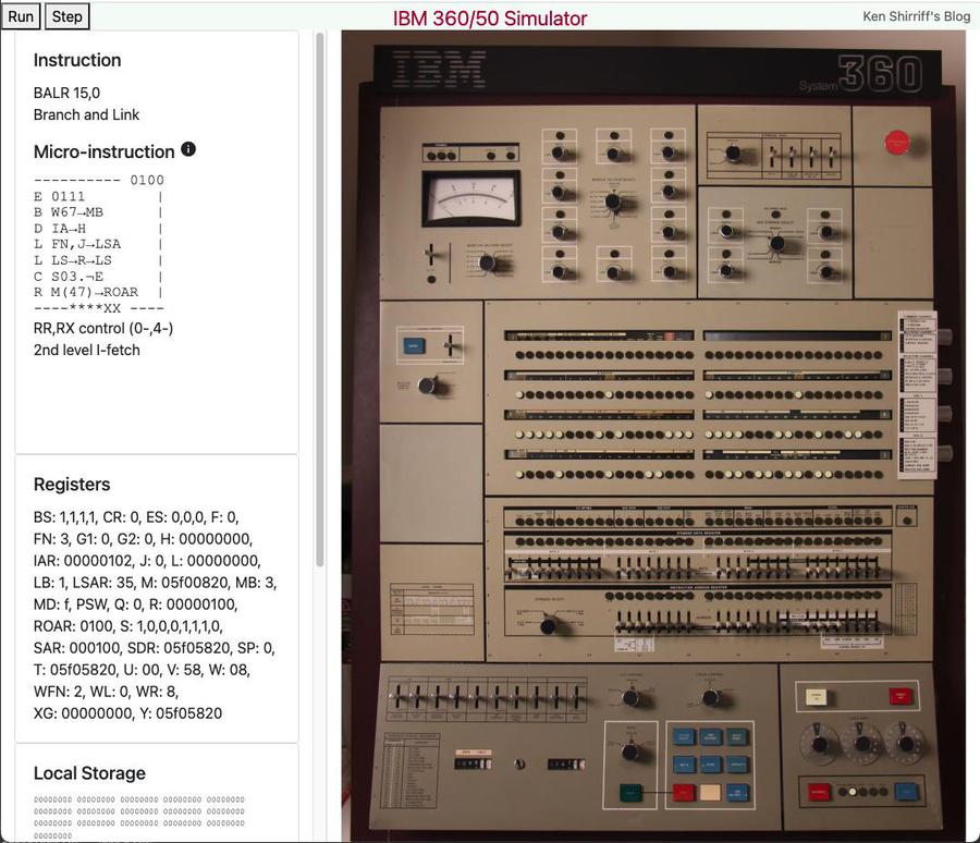
Screenshot of the simulator running in a browser.

Screenshot of the simulator running in a browser.

The radical decision behind System/360 was to use a single architecture for the entire product line of computers.3 The name symbolized “360 degrees to cover the entire circle of possible uses.” Using a common architecture seems obvious now (e.g. x86), but prior to the System/360, IBM (like other computer manufacturers) produced multiple computers with entirely incompatible architectures.

Internally, the different System/360 models had completely different implementations to support a wide range of cost and performance levels: the fastest model was over 1000 times as powerful as the slowest. Low-end models used simple hardware and an 8-bit datapath while advanced models used wide datapaths, fast semiconductor registers, out-of-order instruction execution, and caches.2 Despite these internal differences, the models all looked the same to the programmer.

Architecture of System/3604

You might expect a computer architecture from the 1960s to be simple, but System/360 is remarkably complex, partly because it merged six computer families into one architecture. It is a 32-bit architecture that supports many datatypes. As well as 32-bit integers and half words, it supports decimal arithmetic on numbers up to 31 digits long. Floating-point arithmetic supports short (32 bit), long (64 bit), or extended (128 bit) values. The processor also supports character strings up to 256 bytes long.

The System/360 instruction set has about 100 different instructions and several addressing modes. Some of these instructions are straightforward arithmetic, logic, or control operations. Other instructions are more complex, such as the "character move" that copies up to 256 characters in memory, or the floating-point instructions.

One of the most complex instructions is "edit", which formats a sequence of decimal digits for printing, for example inserting commas, a minus sign, or decimal point; removing leading zeroes, or filling leading spaces with characters. The number 1234567 could be "edited" into the string "$***12,345.67" for printing on a check. Keep in mind that this is a single instruction, not a library function like printf.

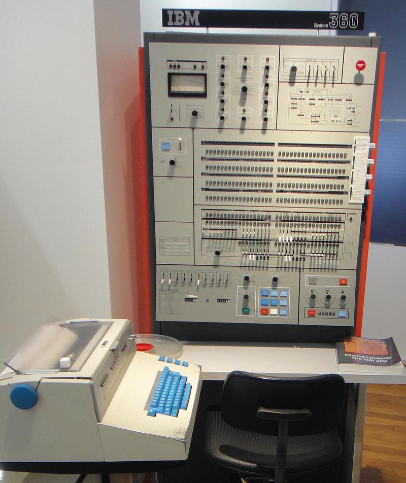
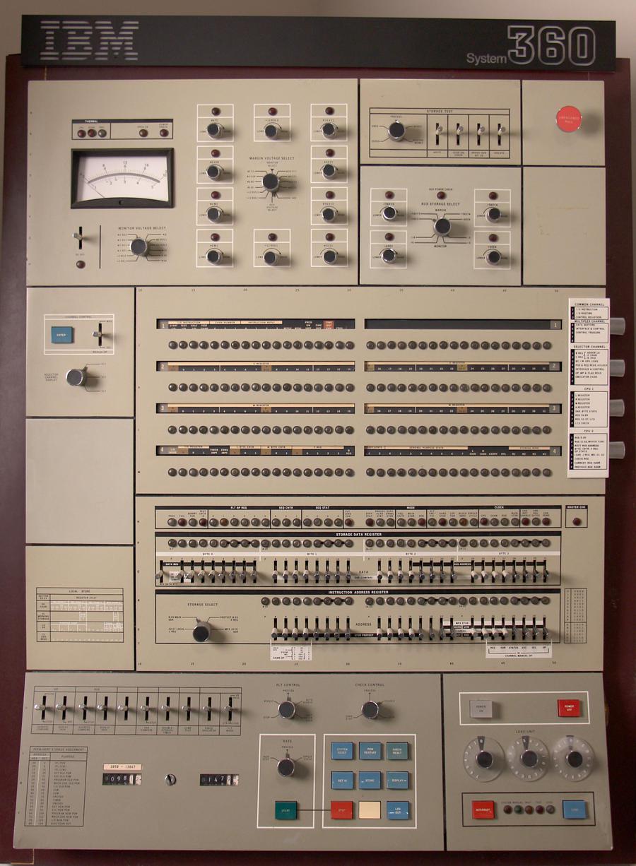
IBM System/360 Model 50 control panel. The dataflow diagram in the upper right illustrates the system's internal design. Photo by Sandstein, CC BY-SA 3.0.

IBM System/360 Model 50 control panel. The dataflow diagram in the upper right illustrates the system's internal design. Photo by Sandstein, CC BY-SA 3.0.

The System/360 architecture also included I/O, defining IBM's "channel" architecture. A channel is a programmable I/O subsystem with its own instruction set. On larger systems, the channel was an independent unit connected to the computer. But smaller systems such as the Model 50 used the same microcode engine to run CPU programs and channel programs.

The point is that System/360 has a large and complex instruction set. A single instruction could result in hundreds of memory accesses and processing steps. The dense instruction set helped programmers to cram programs into the extremely limited core memory of the 1960s. However, the complex instruction set was a problem for the computer designer, who had to implement the complex circuitry to carry out these instructions. The solution was microcode.

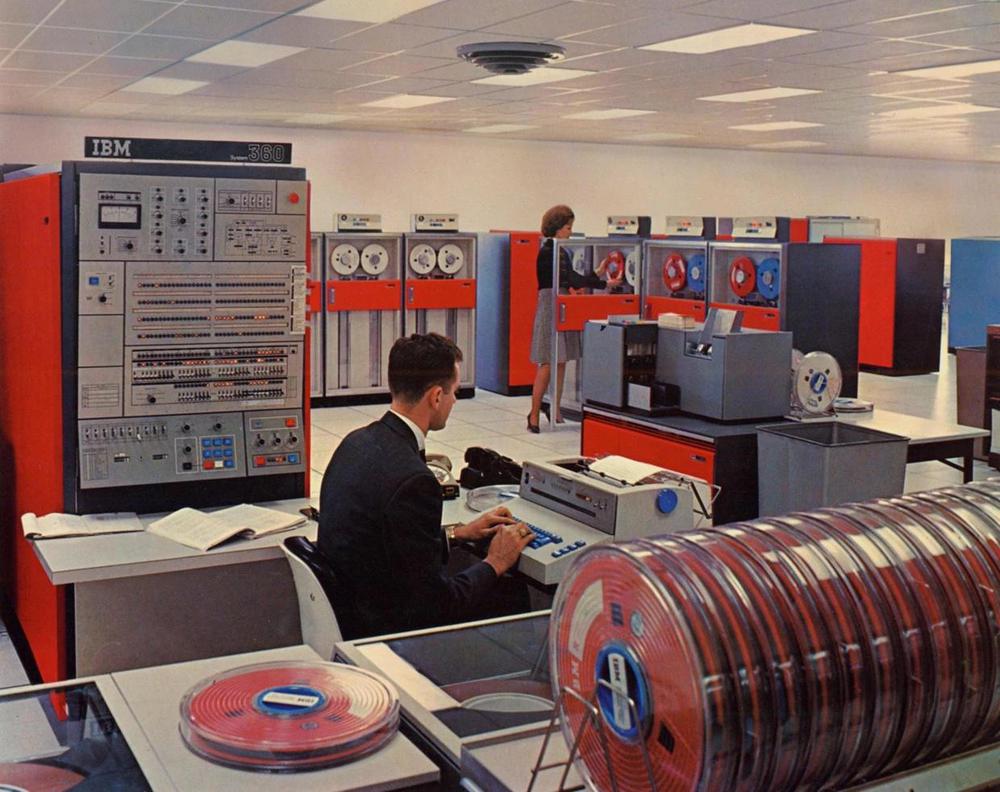
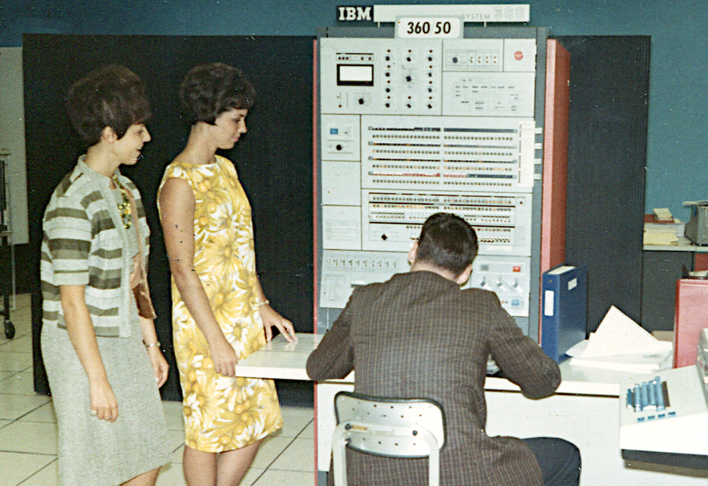
The System/360 Model 50 in a datacenter. The console and processor are at the left. An IBM 1442 card reader/punch is behind the IBM 1052 printer-keyboard that the operator is using. At the back, another operator is loading a tape onto an IBM 2401 tape drive. Photo from IBM.

The System/360 Model 50 in a datacenter. The console and processor are at the left. An IBM 1442 card reader/punch is behind the IBM 1052 printer-keyboard that the operator is using. At the back, another operator is loading a tape onto an IBM 2401 tape drive. Photo from IBM.

Microcode

One of the hardest parts of computer design is creating the control logic that tells each part of the processor how to carry out each instruction. In 1951, Maurice Wilkes came up with the idea of microcode: instead of building the control circuitry from complex logic gates, the control logic could be replaced with code (i. e. microcode) stored in a special memory called a control store. To execute an instruction, the computer internally executes several simpler microinstructions, specified by the microcode. Microcode turns the processor's control logic into a programming task instead of a logic design task.5

Microcode played a key role in the success of the System/360, helping IBM produce a line of computers with the same instruction set architecture but widely different implementations. It also allowed a processor to support different instruction sets; System/360 machines could be backward compatible with customers' older machines6 so customers could keep their existing software. For these reasons, the System/360 computers used microcode unless there was a compelling reason not to.7

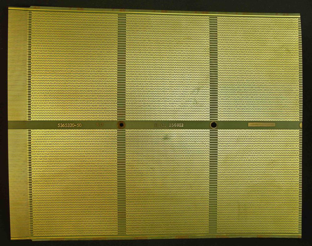
Another advantage of microcode is that it provides an easy way to fix design flaws and bugs in the field. Instead of modifying the hardware, a service engineer could replace the microcode with a new version. The photo below shows a copper sheet with microcode etched into it for the Model 50.

A replaceable BCROS sheet, holding 17,600 bits. Photo courtesy of Glenn's Computer Museum.

A replaceable BCROS sheet, holding 17,600 bits. Photo courtesy of Glenn's Computer Museum.

Microcode can be implemented in a variety of ways. Many computers use "vertical microcode", where a microcode instruction is similar to a machine instruction, just less complicated. The System/360 designs, on the other hand, used "horizontal microcode", with complex, wide instructions of up to 100 bits, depending on the model. These microinstructions were more like a collection of fields, each controlling low-level signals. This improved performance since multiple parts of the processor could be controlled in parallel.

Hardware of the Model 508

The Model 50 was roughly in the middle of the System/360 lineup, providing a powerful mainframe that could be used by a medium-sized business or university department. The Model 50 typically rented for about $18,000 - $32,000 per month (equivalent to $120,000-$200,000 a month in current dollars).

IBM S/360 Model 50. The console was attached to the main frame, about 5 feet deep. The storage frame and power frame are the black cabinets at the back. Photo from Pinterest.

IBM S/360 Model 50. The console was attached to the main frame, about 5 feet deep. The storage frame and power frame are the black cabinets at the back. Photo from Pinterest.

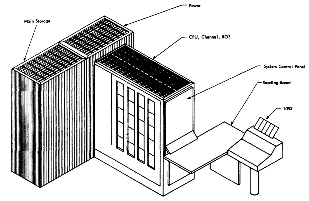
The Model 50 occupied three large cabinets, each 5 feet long, about 2 feet wide, 6 feet tall, and weighing nearly a ton each.9 The main frame, behind the console, contained the CPU, I/O channel circuitry, and the microcode storage. Behind this, the power cabinet contained the computer's power supplies. To the left, the cabinet at the back contained the main storage: one or two core memory modules, each with 128 kilobytes of memory. (I wrote in detail about the Model 50's core memory earlier.) The computer's cables ran under a raised floor to the I/O devices, which typically included tape drives, a card reader, printers, disk drives, I/O controllers, and so forth.

This diagram shows the three frames that made up the basic S/360 Model 50. Source: Model 50 Maintenance Manual page 138.

This diagram shows the three frames that made up the basic S/360 Model 50. Source: Model 50 Maintenance Manual page 138.

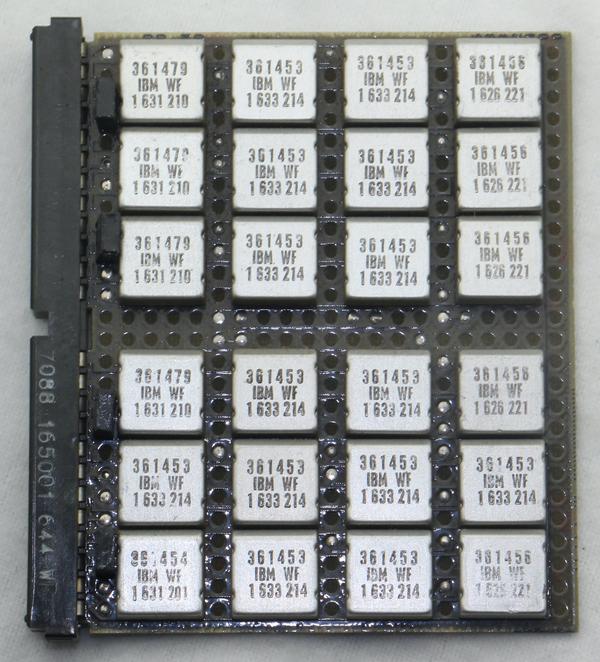
The System/360 processors weren't implemented with integrated circuits, but with SLT (Solid Logic Technology) modules, hybrid modules that contain a few transistors, diodes, and resistors. A typical module implemented a logic gate, so it takes many circuit boards full of modules to construct the processor.

A logic board using SLT modules. Each square metal can is a module.

A logic board using SLT modules. Each square metal can is a module.

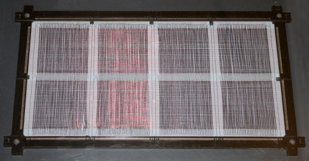
Like most computers of the 1960s, the Model 50 used magnetic core memory, with a tiny ferrite ring to store each bit. The photo below shows a core plane that stores 32768 bits (along with 512 bits for I/O). A stack of 18 planes formed a 64-kilobyte memory module, with two parity bits.10

A Model 50 core plane is arranged as a grid of cores. The Y lines run horizontally. X and sense/inhibit lines run vertically. The sense/inhibit lines form loops at the top and bottom. Each of the four vertical pairs of blocks has separate sense/inhibit lines. Each core plane was about 10¾ × 6¾ × ⅛ inches.

A Model 50 core plane is arranged as a grid of cores. The Y lines run horizontally. X and sense/inhibit lines run vertically. The sense/inhibit lines form loops at the top and bottom. Each of the four vertical pairs of blocks has separate sense/inhibit lines. Each core plane was about 10¾ × 6¾ × ⅛ inches.

The Model 50's internal architecture

To the programmer, all processors within System/360 look the same; internal circuitry, however, may be entirely different.

It's important to keep in mind that the internal architecture of the Model 50 is very different from the architecture that the programmer sees.11 In particular, the processor's internal registers are invisible to the programmer. The programmer instead sees 16 general-purpose registers and 4 floating-point registers, but to the processor these are part of the 64-word local store, a small high-speed core memory.

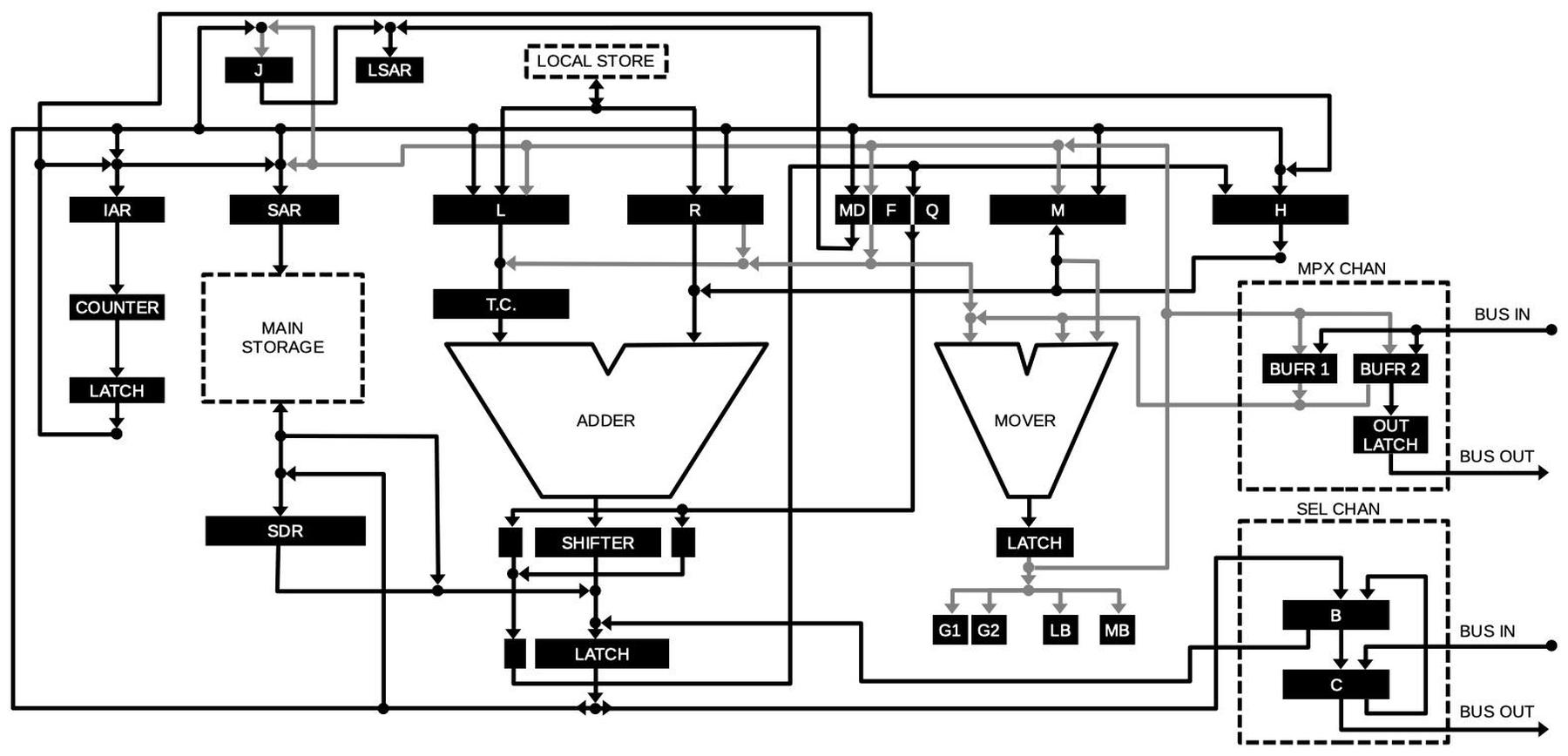
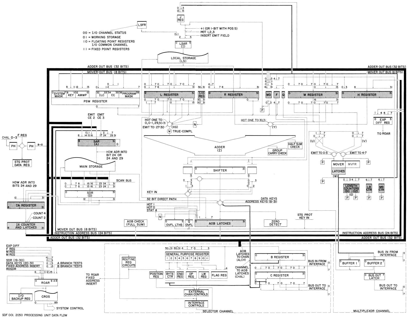
The diagram below shows the complex data flow through the computer.12 The black boxes are internal registers; the processor has a surprisingly large number of registers, used for a variety of purposes. The internal components are connected by buses. Most of the internal communication is over the 32-bit buses, shown in black. The 8-bit "mover" bus is shown in gray.

This diagram shows the data flow through the IBM 360/50 and appears in the upper-right corner of the console. I drew this version since I couldn't find a clear photo of it.

This diagram shows the data flow through the IBM 360/50 and appears in the upper-right corner of the console. I drew this version since I couldn't find a clear photo of it.

The heart of the computer is the 32-bit adder, which performs addition. For subtraction, the argument is complemented by the True/Complement circuit (TC). The adder has an associated shifter to perform bit-shifts; this is especially important for multiplication, division, and floating-point calculations. Operating in parallel with the adder is the "mover", which operates on bytes. It can extract a byte from a 32-bit word, as well as manipulating 4-bit pieces of the byte. The mover also performs Boolean operations (AND, OR, XOR). (Unlike most processors, the Model 50 separates arithmetic and logical operations, instead of having an ALU perform both.)

The computer's main core-memory storage is on the left. To access memory, an address is put in the Storage Address Register (SAR). Data is then read or written through the Storage Data Register (SDR). To the left of main storage, is the Instruction Address Register (the Program Counter or PC in modern terms). At the top is the Local Store, 64 words of high-speed core memory that holds the programmer's registers as well as some internal storage. The local store is accessed through the Local Store Address Register (LSAR).

At the right are the I/O channels: the low-speed Multiplexor Channel and the high-speed Selector Channel. You can think of these as DMA (direct memory access) paths for I/O. The multiplexor channel communicates over an 8-bit bus through the mover, while the selector channel communicates over a 32-bit bus. Although the channels are conceptually separate from the processor, the channels use the same buses, circuitry, and microcode engine as the processor. This limits I/O performance compared to more advanced System/360 models that have independent circuitry for the channels.

An example of the microcode

As you can see, the processor has many registers and functional units. The microcode needs to control these components to carry out program instructions. The microcode architecture is very complex and takes over 100 pages to explain thoroughly,15 so I'm only able to scratch the surface here. Each microinstruction is 90 bits long and performs multiple tasks. In the documentation, IBM used an 11-line block to represent each microinstruction, showing all the activities that are taking place in parallel.

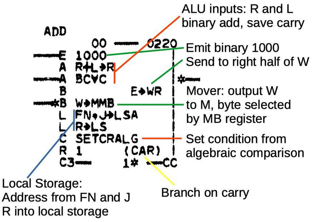
A sample microinstruction is shown below, part of the microcode that implements an add instruction. At this point, earlier microinstructions have fetched and decoded the instruction and put the arguments into the R and L registers. This microinstruction performs the actual 32-bit addition, but there's a lot more happening than just the addition.

One microinstruction, part of the integer addition code. This microinstruction is at micro-address 0220.

One microinstruction, part of the integer addition code. This microinstruction is at micro-address 0220.

Starting with the line "R+L→R" (red), this indicates that the ALU is taking inputs from registers R and L, and the result is going into the R register. In other words, the two arguments are added. The result R is stored into the desired programmer-visible register in local storage (blue). The processor registers FN and J select the address in local storage. Meanwhile, the SETCRALG line sets the Condition code register based on the sign (i.e. "algebraic" value) of the result, indicating if the result is positive, negative, or zero.

The line "BC⩝C" indicates that signed overflow is detected and used as the carry flag14 while CAR (yellow) indicates the microcode branches on this carry (overflow) value. Thus, the microcode will take one path if the addition was valid and a second error path if overflow occurred. A microinstruction can "emit" an arbitrary 4-bit value (green) which can be used in a variety of ways. In this case, the binary value 1000 is emitted, fed into the W register, and then the M register, for use by the next microinstruction. As you can see, the CPU performs many activities in parallel for one microinstruction, which increases the computer's performance.

All the activities of a microinstruction are encoded into a 90-bit word consisting of 28 fields.13 The microinstruction discussed above (micro-address 0220) is highlighted in the documentation below. A single microinstruction is very complex, which is why it takes an 11-line block of text to represent it.

Part of the microcode listing. The previously-discussed microinstruction is highlighted. Note that the micro-address 0220 matches the address in the upper-left corner of the microinstruction diagram.

Part of the microcode listing. The previously-discussed microinstruction is highlighted. Note that the micro-address 0220 matches the address in the upper-left corner of the microinstruction diagram.

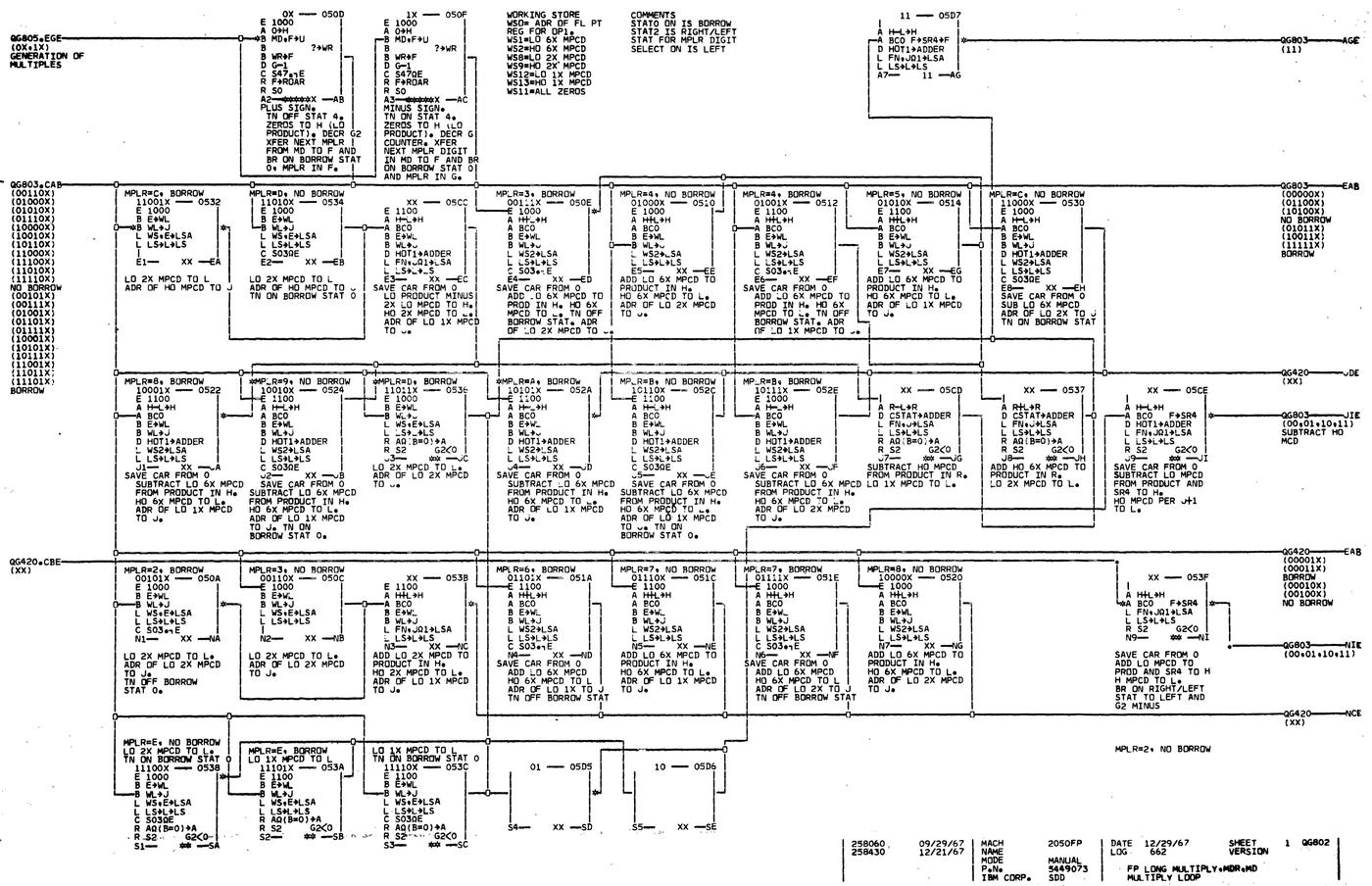
The processor documentation contains hundreds of pages of microcode;16 one page of the floating-point multiply code is below. Each box is one microinstruction, and the lines between them indicate the complex control paths. I'm not going to explain this microcode,17 but I wanted to show its complexity.

Part of the floating-point multiply microcode. (Click for a larger view.) From ALD vol 18.

Part of the floating-point multiply microcode. (Click for a larger view.) From ALD vol 18.

The console

The discussion above has shown the complex internal architecture of the Model 50. The numerous lights and controls on the console19 provide a view into this internal state. There were three main uses for the console. The first use was basic "operator control" tasks such as turning the system on, booting it, or powering it off, using the controls in the lower section of the console. These controls were consistent across the S/360 line and were usually the only controls the operator needed. The three hexadecimal dials in the lower right selected the I/O unit that held the boot software. Once the system had booted, the operator generally typed commands into the system rather than using the console.

Control panel of the IBM System/360 Model 50. This panel has marginal check controls for auxiliary storage in the upper right, replacing the dataflow diagram.

Control panel of the IBM System/360 Model 50. This panel has marginal check controls for auxiliary storage in the upper right, replacing the dataflow diagram.

The second console function was "operator intervention": program debugging tasks such as examining and modifying memory or registers and setting breakpoints. The lights and toggle switches in the lower half of the console were used for operator intervention. The operator could enter a 24-bit address using the row of 24 toggle switches, and enter a 32-bit data value using the row of 32 toggle switches above. The lights allowed the contents of memory to be examined. With other switches, the operator could set a breakpoint, single-step through a program, and perform other debugging operations.

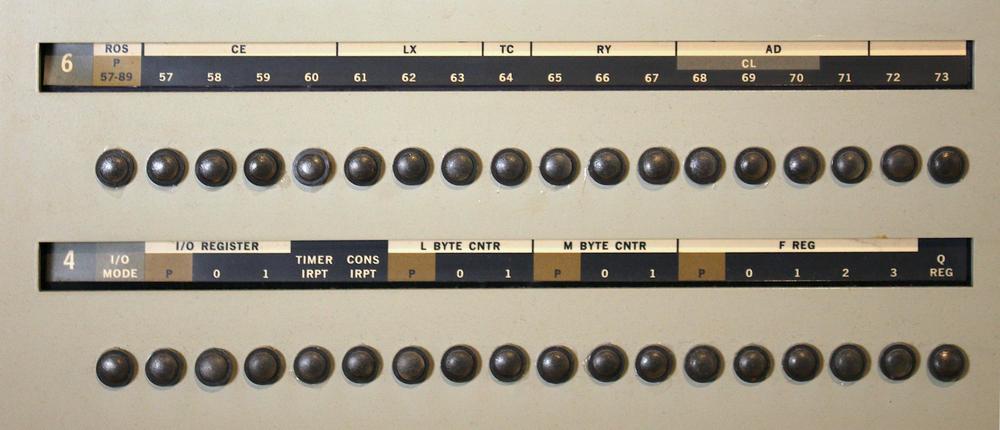
The third console function was system maintenance and repair performed by an IBM customer engineer. The customer engineering displays took up the top half of the console and provided detailed access to the computer's complex internal state. To save space, the Model 50 had four roller knobs on the right side, with 8 positions for each knob. Each knob position selected a different function for the row of 36 lights (32 bits plus parity). The legends above the lights rotate with the knobs, showing the meaning of each light. For example, one position would display the L register, while another position would display the current microinstruction. In the photo below, the upper roller and lights are displaying part of the microcode currently being executed (ROS = Read Only Store). The roller below shows some of the internal registers and counters.

Closeup of two rollers and the associated lights.

Closeup of two rollers and the associated lights.

Finally, the voltmeter and voltage control knobs in the upper left of the console were used by an IBM customer engineer for "marginal checking". By raising and lowering the voltage levels, borderline components could be detected and replaced before they caused problems.

The simulator

The simulator is at righto.com/360 and the code is on Github. I implemented the simulator in JavaScript so it can run in a browser. It runs a sample program by executing the Model 50's microcode, simulating each microinstruction and the hardware. Each microinstruction is displayed graphically, along with the current instruction, the registers, the local storage, and core memory. It displays the console lights accurately based on the internal state, on a zoomable virtual console. Each row of lights can display 8 different elements, which you can change by clicking on a roller. You can step also through the microcode, one microinstruction at a time.

This simulator is still under development so don't expect it to work perfectly. I also haven't implemented the toggle switches, so you can't enter a program from the console yet. I also need to implement the I/O system, which has its own registers and a different microcode format.

To build the simulator, I extracted the binary microcode from the listings using a custom OCR tool. I implemented the hundreds of micro-operations, which were tricky to get correct. While most micro-operations are simple operations such as moving a register to the bus, some microinstructions are much more complex, especially for floating-point operations.20 Another complication is that a microinstruction performs many tasks in parallel and it was hard to determine the exact order in which to perform them.

My eventual goal with the simulator is to move it into the physical world. Specifically, I plan to drive the lights on CuriousMarc's Model 50 control panel to make the panel operate accurately. We also plan to hook up his IBM tape drives and card reader so we can have all the pieces of a Model 50 mainframe working together, except for the processor itself. I plan to port the simulator to C so I can run it in a microcontroller to drive the physical console. An FPGA implementation is another possibility; this would provide the maximum speed, but would be harder to implement.

I announce my latest blog posts on Twitter, so follow me @kenshirriff for updates and future articles. I also have an RSS feed. Thanks to Richard Cornwell for discussion and data.

Notes and references

  1. My simulator is not particularly useful unless you really care about the microcode in the Model 50. If you want to run software on a simulated System/360, you probably want to use the Hercules system

  2. I'll briefly summarize some of the different implementations used in System/360 computers.

    The low-end Model 30 uses an 8-bit bus and ALU, so 32-bit operations take four steps. It uses 60-bit microcode.

    The Model 40 also has an 8-bit bus and ALU, but it has 16-bit registers and a 16-bit bus to memory, improving the performance. It has 60-bit microcode.

    The Model 50 (discussed in this blog post) has 32-bit registers, memory bus, and adder. It also has the 8-bit mover that can operate in parallel with the adder.

    The Model 65 has a 64-bit bus, and multiple adders (60 and 8-bit) that allow a floating-point fraction and exponent to be processed in parallel. It also has an 8-byte instruction buffer and external channels. It uses 100-bit microcode.

    The Model 75 has a 64-bit main adder, 8-bit exponent adder, 8-bit decimal adder, and a 24-bit addressing adder. It overlaps instruction fetching and execution, with 16 bytes of instruction prefetching and 8 bytes of data prefetching.

    The high-end Model 91 has an advanced superscalar architecture with out-of-order execution, instruction pipelining, and multiple arithmetic execution units. Higher models support memory interleaving for faster access: 2-way on the Model 65 up to 16-way on the Model 195.

    The models 44, 75, 91 and above used hardwired control instead of microcode to squeeze out more performance.

    As you can see, the System/360 line has a wide variety of implementations. At the low end, the hardware is kept to a minimum to reduce costs, while at the high end, more hardware boosts performance, with wider datapaths and multiple functional units providing parallelism. 

  3. The System/360 line didn't completely meet the goal of a compatible architecture. IBM split out the business and scientific markets on the low-end machines by marketing subsets of the instruction set. The basic instructions were provided in the "standard" instruction set. On top of this, decimal instructions (for business) were in the "commercial" instruction set and floating-point was in the "scientific" instruction set. The "universal" instruction set provided all these instructions plus storage protection (i.e. memory protection between programs). Additionally, cost-cutting on the low-end Model 20 made it incompatible with the S/360 architecture, and the Model 44 was somewhat incompatible to improve performance on scientific applications. 

  4. IBM defined the System/360 architecture in great detail in a document called the IBM System/360 Principles of Operation. It describes not only the instruction set, but also the datatypes, input/output model, the interrupt model, and even the basic structure of the system control panel. To learn more about System/360, see A Programmer's Introduction to the IBM System/360 Architecture, Instructions, and Assembler Language. A bunch of assembly examples are at rosettacode

  5. The primary benefit of microcode for IBM was economic. As described in Microprogram Control for System/360, the cost of a non-microcoded processor is roughly linear in the size of the instruction set. However, a microcoded system has a roughly fixed cost, with a small overhead for additional instructions. Thus, as instruction sets get more complex (as in System/360), there is a crossover point where microcode is more efficient. This is especially the case for smaller systems where the base cost is lower. The lower marginal cost also makes emulating other systems more feasible. The IBM System/360 was one of the first commercial computers to make extensive use of microcode. 

  6. Various System/360 machines supported compatibility features with earlier IBM computers including the 1401, 1440, 1620, 7070, 7074, 7080, 709, 7090, 7094. Generally, a smaller System/360 machine could replace a smaller IBM computer such as the 1401, while a larger mainframe such as the 7090 needed to be replaced by a larger System/360 computer such as the Model 65.  

  7. A few System/360 models did not use microcode. The Model 44 was designed as a high-performance computer for scientific applications, so it used hardwired control. The Model 85 was partially microcoded, while the Models 75 and 91 were completely hardwired. 

  8. The book IBM's 360 and Early 370 Systems describes the history of the S/360 in great detail. IBM lists data on each model, including dates, data flow width, cycle time, storage, and microcode size. Another list with model details is here. The article System/360 and Beyond has lots of info. A list of 360 models and brief descriptions is here. For information on the Model 50 specifically, see the Functional Characteristics manual, Field Engineering manuals, Wikipedia, photos here and here, CuriousMarc video

  9. For detailed dimensions of the System/360 components, see the Physical Planning Manual For more memory, another 1500-pound frame could be added to the Model 50, boosting it from 256 kilobytes of memory to 512 kilobytes. Up to four Large Capacity Storage units (IBM 2361) could be added, each providing two more megabytes. 

  10. I wrote in detail about the Model 50's core memory system here

  11. The quote is from System/360 Model 40 comprehensive introduction

  12. The Model 50 Field Engineering Diagram Manual contains the detailed data flow diagram below. This diagram corresponds to the diagram discussed earlier, but provides much more detail. In particular, it shows the exact bit widths of the various data paths and registers.

    The detailed data flow diagram. Click for a larger version.

    The detailed data flow diagram. Click for a larger version.


  13. The table below shows how a microinstruction is encoded into a 90-bit word.

    BitsNameMeaning
    0PParity
    1-3LUMover input left side
    4-5MVMover input right side
    6-11ZPROAR address (Read Only storage Address Register)
    12-15ZFROAR branch control
    16-18ZNAddress control field
    19-23TRAdder control
    24Unused
    25-27WSLocal store address control
    28-30SFLocal store functions
    31PParity
    32-34IVInvalid digit test
    35-39ALAdder latch gating
    40-43WMMover destination
    44-45UPByte counter function
    46MDMD counter control
    47LBL byte counter control
    48MBM byte counter control
    49-51DGLength counter
    52-53ULMover function left digit
    54-55URMover function right digit
    56PParity
    57-60CEEmit field
    61-63LXLeft adder input
    64TCTrue or complement control
    65-67RYRight adder input
    68-71ADAdder function control
    72-77ABA branch control
    78-82BBB branch control
    83Unused
    84-89SSStat setting control

    For channel instructions, the microcode format is slightly different since some of the fields need to control the channel circuitry. However, most of the fields are the same as for the CPU. The table below shows the microcode format for the channel; the highlighted entries are different from the CPU microcode.

    BitsNameMeaning
    0PParity
    1-3LUMover input left side
    4-5MVMover input right side
    6-11ZPROAR address
    12-15ZFROAR branch control
    16-18ZNAddress control field
    19-23TRAdder control
    24Unused
    25CSLocal storage address selector
    26-27SALocal storage address
    28-30SFLocal storage function
    31PParity
    32-34CTTiming signals to channel
    35-39ALAdder latch gating
    40-42WLMover destination
    43-46HCMultiplexor channel stat setting
    47-48CGControl signals to channel
    49-51MGMultiplexor channel gate control
    52-53ULMover function left digit
    54-55URMover function right digit
    56PParity
    57-60CEEmit field
    61-63LXLeft adder input
    64TCTrue or complement control
    65-67RYRight adder input
    68-70CLSelector channel adder latch tests
    71Unused
    72-77ABA branch control
    78-82BBB branch control
    83Unused
    84-89SSStat setting control
     

  14. When adding twos-complement signed numbers, an overflow occurs if the carry out of the most significant bit is different from the carry out of the second-most-significant bit. (I explain this in detail here.) IBM numbers the bits in a word "backward" with bit 0 the most significant. Thus, an overflow occurs if the carry from bit 0 XOR'd with the carry from bit 1 is nonzero. IBM uses ⩝ to indicate an exclusive or. Thus, CARRY(0) ⩝ CARRY(1) indicates an overflow, represented as BC⩝C in the microcode. 

  15. For a description of how the Model 50 microcode works, see the book "Microprogramming: Principles and Practices", S. Husson (1970), pages 295 to 411. Bitsavers has a lot of Model 50 documents, but not everything. If you have additional documentation, such as the IBM Automated Logic Diagrams, please let me know. 

  16. The Model 50's microcode listing is available in three volumes on bitsavers. The binary microcode listings are difficult to read with OCR because pages were printed on different printers; some use serif fonts and others use sans-serif fonts. I made my own OCR program designed to process binary, which was able to read the listings for the most part. The presence of parity in the microcode helped catch errors. 

  17. Ok, I'll give a brief explanation of that page of microcode, which is part of the implementation of floating-point multiplication. The implementation is designed with tradeoffs between speed, code length, and temporary memory usage. The idea is to multiply the multiplicand by the multiplier, kind of like long multiplication on paper, where you multiply a digit at a time and add the partial sums. This code processes a hex digit of the multiplier at a time, with a separate case for each digit. The multiplicand is multiplied by the digit and this is added to the running total, shifting as appropriate. To make this fast, multiples of the multiplicand are pre-computed. However, pre-computing 16 multiples (one for each hex digit value) would take too much temporary (local) storage. So the only pre-computed multiples are 1, 2, and 6, and these are combined for other digits. To multiply by the digit 7, for instance, the multiples for 1 and 6 are added. To multiply by the digit 4, the multiple for 6 is added and the multiple for 2 is subtracted.

    But what about multiplying by 9 through 15? The trick is to "borrow" 16 from the next-higher digit. For instance, to multiply by the digit 11, you borrow 16, subtract the multiple for 6, and add the multiple for 1. Then the value one less is used for the next digit to account for the borrow. Thus, all 16 possibilities can be handled by adding or subtracting at most two of the pre-computed values. With borrowing, the code needs to handle 32 cases; the included page implements 22 of these cases. This implementation makes multiplication rapid, but the microcode is complex with many paths. (There is also a bunch more code to handle the floating-point exponent, normalizing values, overflow, underflow, and so forth.) 

  18. Different System/360 models used a variety of methods to store microcode.18 An important feature of IBM's microcode storage was that the microcode could be replaced in the field. The low-end Model 25 held microcode in a 16-kilobyte section of core memory called Control Storage. The Model 30 used CCROS (Card Capacitor Read-only Store), storing the microcode on special metalized punch cards that were read capacitively. Transformer Read-Only Storage (TROS, below) was used by the System/360 Model 20 and Model 40. I wrote an article about microcode storage if you want more information.

    A TROS module from an IBM System/360 Model 20.

    A TROS module from an IBM System/360 Model 20.

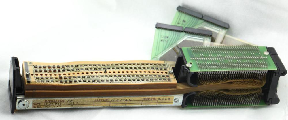
    The Model 50 (as well as 65 and 67) stored microcode in BCROS (Balanced Capacitor Read-Only Storage), using copper-clad epoxy glass laminate boards, each 20″×8½″. Each sheet plane held 176 words of 100 bits, and the Model 50 used 16 sheets to store 2816 words. (Only 90 of the 100 bits in each word were used.) The data in BCROS was etched into the copper wiring (below). Each bit is represented by two squares: one connected to the upper wire and one connected to the lower wire (or vice versa), forming the balanced capacitors.

    Closeup of a BCROS sheet from a System/360 Model 50.

    Closeup of a BCROS sheet from a System/360 Model 50.


  19. The features of the system control panel were carefully defined in the System/360 Principles of Operation pages 117-121, providing a consistent operator experience across the S/360 line. (The customer engineering part of the panel, on the other hand, was not specified and wildly different across the product line.) Diagrams of S/360 consoles are at quadibloc. For more details on the consoles, see my article on System/360 consoles

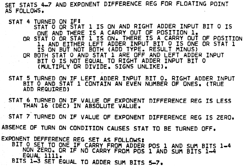
  20. The micro-operation that caused me the most difficulty is ED*FP, which computes the difference between two exponents for floating-point, but also computes four floating-point flags including the sign depending on the type of operation. Not only is this operation complex, but I think there is a typo in the description.

    A description of the ED*FP micro-operation.

    A description of the ED*FP micro-operation.

    Another complex micro-operation is MLJK, which performs multiple actions as part of instruction decoding:

    Gate adder latch to L reg and M reg. Gate latch bits 12-15 to J reg. Gate latch bits 16-19 to MD counter. Turn off refetch stat.
    If latch bits 12-15 all zero, turn on stat 0. Otherwise turn off stat 0.
    If latch bits 16-19 all zero, turn on stat 1. Otherwise turn off stat 1.
    If latch bits 16-17 all zero, turn on one-syllable stat. Otherwise turn off one-syllable stat.
    If latch bits 0-1 equal 00, set ILC to 01.
    If latch bits 0-1 equal 01 or 10, set ILC to 10.
    If latch bits 0-1 equal 11, set ILC to 11. 

Silicon die teardown: a look inside an early 555 timer chip

If you've played around with electronic circuits, you probably know the 555 timer integrated circuit,1 said to be the world's best-selling integrated circuit with billions sold. Designed by analog IC wizard Hans Camenzind2, the 555 has been called one of the greatest chips of all time.

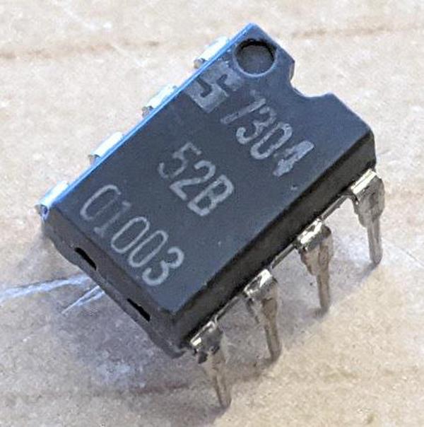
An 8-pin 555 timer with a Signetics logo. It doesn't have a 555 label, but instead is labeled "52B 01003" with a 7304 date code, indicating week 4 of 1973. Photo courtesy of Eric Schlaepfer.

An 8-pin 555 timer with a Signetics logo. It doesn't have a 555 label, but instead is labeled "52B 01003" with a 7304 date code, indicating week 4 of 1973. Photo courtesy of Eric Schlaepfer.

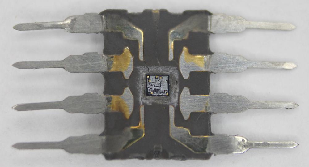
Eric Schlaepfer (@TubeTimeUS) recently came across the chip above, with a mysterious part number. He tediously sanded through the epoxy package to reveal the die (below) and determined that the chip is a 555 timer. Signetics released the 555 timer in mid-1972 4 and the chip below has a January 1973 date code (7304), so it must be one of the first 555 timers. Curiously, it is not labeled 555, so perhaps it is a prototype or internal version.3 I took detailed die photos, which I discuss in this blog post.

The 555 timer with the package sanded down to expose the silicon die, the tiny square in the middle.

The 555 timer with the package sanded down to expose the silicon die, the tiny square in the middle.

A brief explanation of the 555 timer

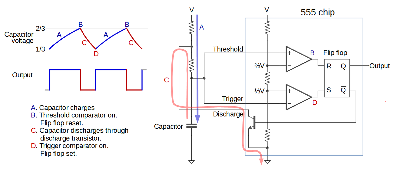
The 555 timer has hundreds of applications, operating as anything from a timer or latch to a voltage-controlled oscillator or modulator. The diagram below illustrates how the 555 timer operates as a simple oscillator. Inside the 555 chip, three resistors form a divider generating references voltages of 1/3 and 2/3 of the supply voltage. The external capacitor will charge and discharge between these limits, producing an oscillation. In more detail, the capacitor will slowly charge (A) through the external resistors until its voltage hits the 2/3 reference. At that point (B), the upper (threshold) comparator switches the flip flop off and the output off. This turns on the discharge transistor, slowly discharging the capacitor (C). When the voltage on the capacitor hits the 1/3 reference (D), the lower (trigger) comparator turns on, setting the flip flop and the output, and the cycle repeats. The values of the resistors and capacitor control the timing, from microseconds to hours.5

Diagram showing how the 555 timer can operate as an oscillator. The external capacitor charges and discharges through the external resistors, under the control of the 555 timer.

Diagram showing how the 555 timer can operate as an oscillator. The external capacitor charges and discharges through the external resistors, under the control of the 555 timer.

To summarize, the key components of the 555 timer are the comparators to detect the upper and lower voltage limits, the three-resistor divider to set these limits, and the flip flop to keep track of whether the circuit is charging or discharging. The 555 timer has two other pins (reset and control voltage) that I haven't covered above; they can be used for more complex circuits.

The structure of the integrated circuit

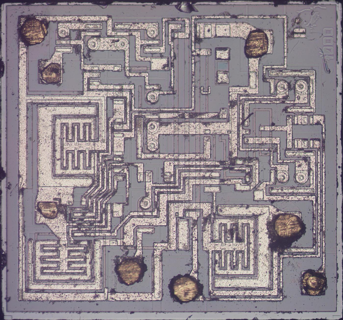
I created the photo below from a composite of microscope images. On top of the silicon, a thin layer of metal connects different parts of the chip. This metal is clearly visible in the photo as light-colored traces. Under the metal, a thin, glassy silicon dioxide layer provides insulation between the metal and the silicon, except where contact holes in the silicon dioxide allow the metal to connect to the silicon. At the edge of the chip, thin wires connect the metal pads to the chip's external pins.

Die photo of the 555 timer. Click this image (or any other) for a larger version.

Die photo of the 555 timer. Click this image (or any other) for a larger version.

The different types of silicon on the chip are harder to see. Regions of the chip are treated (doped) with impurities to change the electrical properties of the silicon. N-type silicon has an excess of electrons (negative), while P-type silicon lacks electrons (positive). In the photo, these regions show up as a slightly different color surrounded by a thin black border. These regions are the building blocks of the chip, forming transistors and resistors.

NPN transistors inside the IC

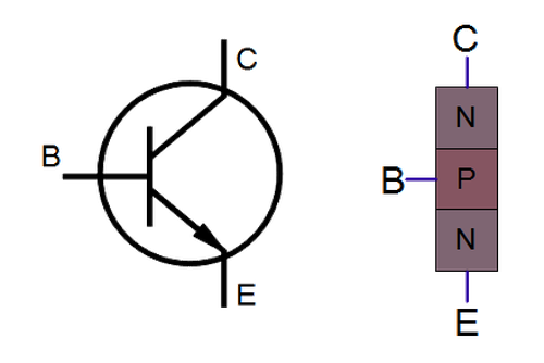
Transistors are the key components in a chip. The 555 timer uses NPN and PNP bipolar transistors. If you've studied electronics, you've probably seen a diagram of an NPN transistor like the one below, showing the collector (C), base (B), and emitter (E) of the transistor, The transistor is illustrated as a sandwich of P silicon in between two symmetric layers of N silicon; the N-P-N layers make an NPN transistor. It turns out that transistors on a chip look nothing like this, and the base often isn't even in the middle!

Schematic symbol for an NPN transistor, along with an oversimplified diagram of its internal structure.

Schematic symbol for an NPN transistor, along with an oversimplified diagram of its internal structure.

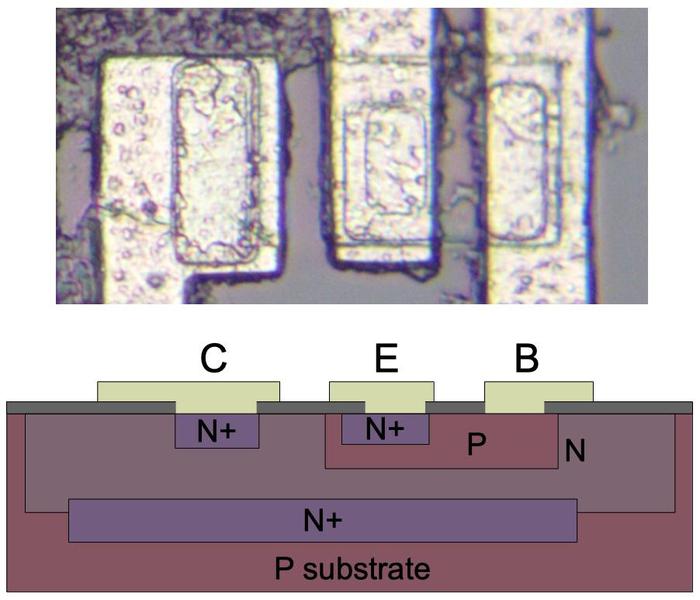
The photo below shows a closeup of one of the transistors in the 555 as it appears on the chip. The slightly different tints in the silicon indicate regions that have been doped to form N and P regions. The whitish areas are the metal layer of the chip on top of the silicon - these form the wires connecting to the collector, emitter, and base.

Structure of an NPN transistor on the die.

Structure of an NPN transistor on the die.

Underneath the photo is a cross-section drawing illustrating how the transistor is constructed. There's a lot more than just the N-P-N sandwich you see in books, but if you look carefully at the vertical cross-section below the 'E', you can find the N-P-N that forms the transistor. The emitter (E) wire is connected to N+ silicon. Below that is a P layer connected to the base contact (B). And below that is an N+ layer connected (indirectly) to the collector (C).6 The transistor is surrounded by a P+ ring that isolates it from neighboring components.

PNP transistors inside the IC

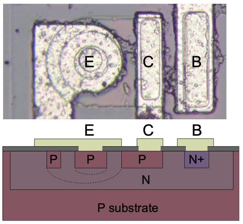
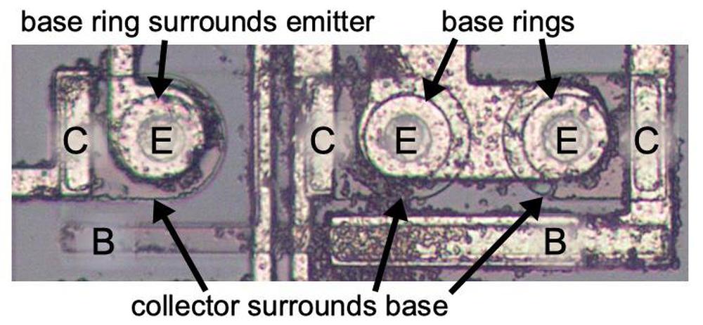
You might expect PNP transistors to be similar to NPN transistors, just swapping the roles of N and P silicon. But for a variety of reasons, PNP transistors have an entirely different construction. They consist of a small circular emitter (P), surrounded by a ring-shaped base (N), which is surrounded by the collector (P). This forms a P-N-P sandwich horizontally (laterally), unlike the vertical structure of the NPN transistors.

The diagram below shows one of the PNP transistors in the 555, along with a cross-section showing the silicon structure. Note that although the metal contact for the base is on the edge of the transistor, it is electrically connected through the N and N+ regions to its active ring in between the collector and emitter.

A PNP transistor in the 555 timer chip. Connections for the collector (C), emitter (E) and base (B) are labeled, along with N and P doped silicon. The base forms a ring around the emitter, and the collector forms a ring around the base.

A PNP transistor in the 555 timer chip. Connections for the collector (C), emitter (E) and base (B) are labeled, along with N and P doped silicon. The base forms a ring around the emitter, and the collector forms a ring around the base.

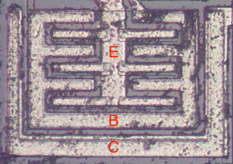
The output transistors in the 555 are much larger than the other transistors and have a different structure in order to produce the high-current output. The photo below shows one of the output transistors. Note the multiple interlocking "fingers" of the emitter and base, surrounded by the large collector.

A large, high-current NPN output transistor in the 555 timer chip. The collector (C), base (B) and emitter (E) are labeled.

A large, high-current NPN output transistor in the 555 timer chip. The collector (C), base (B) and emitter (E) are labeled.

How resistors are implemented in silicon

Resistors are a key component of analog chips. Unfortunately, resistors in ICs are large and inaccurate; the resistances can vary by 50% from chip to chip. Thus, analog ICs are designed so only the ratio of resistors matters, not the absolute values, since the ratios remain nearly constant.

A resistor inside the 555 timer. The resistor is a strip of P silicon between two metal contacts.

A resistor inside the 555 timer. The resistor is a strip of P silicon between two metal contacts.

The photo above shows a 10KΩ resistor in the 555, formed from a strip of P silicon (pinkish gray), contacting metal wiring at either end. Other metal wires cross the resistor. The resistor has a spiral shape to fit its length in the available space. The resistor below is a 100KΩ pinch resistor. A layer of N silicon on top of the pinch resistor makes the conductive region much thinner (i.e. pinches it), forming a much higher but less accurate resistance.

A pinch resistor inside the 555 timer. The resistor is a strip of P silicon between two metal contacts. An N layer on top pinches the resistor and increases the resistance. This resistor is crossed by a vertical metal line.

A pinch resistor inside the 555 timer. The resistor is a strip of P silicon between two metal contacts. An N layer on top pinches the resistor and increases the resistance. This resistor is crossed by a vertical metal line.

IC component: The current mirror

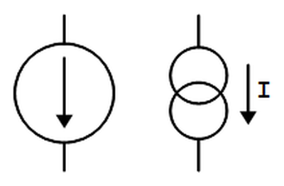
There are some subcircuits that are very common in analog ICs, but may seem mysterious at first. The current mirror is one of these. If you've looked at analog IC block diagrams, you may have seen the symbols below, indicating a current source, and wondered what a current source is and why you'd use one. The idea is you start with one known current and then you can "clone" multiple copies of the current with a simple transistor circuit, the current mirror.

Schematic symbols for a current source.

Schematic symbols for a current source.

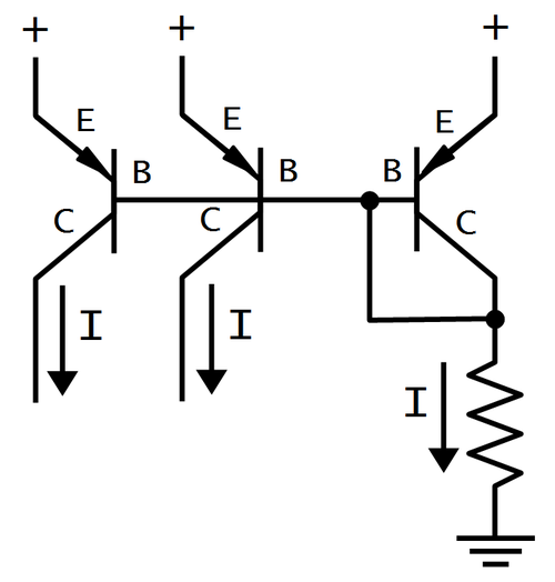
The following circuit shows how a current mirror is implemented with two identical transistors.7 A reference current passes through the transistor on the right. (In this case, the current is set by the resistor.) Since both transistors have the same emitter voltage and base voltage, they source the same current, so the current on the right matches the reference current on the left.8

Current mirror circuit. The current on the right copies the current on the left.

Current mirror circuit. The current on the right copies the current on the left.

A common use of a current mirror is to replace resistors. As explained earlier, resistors inside ICs are both inconveniently large and inaccurate. It saves space to use a current mirror instead of a resistor whenever possible. Also, the currents produced by a current mirror are nearly identical, unlike the currents produced by two resistors.

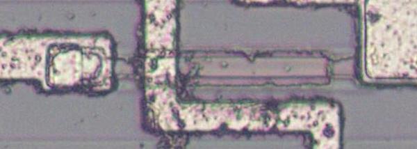
Three transistors form a current mirror in the 555 timer chip. They all share the same base and two transistors share emitters.

Three transistors form a current mirror in the 555 timer chip. They all share the same base and two transistors share emitters.

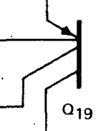
The three transistors above form a current mirror with two outputs. Note the three transistors share the base connection, tied to the collector on the right, and the emitters on the right are tied together. On the schematic, the two transistors on the right are drawn as a single two-collector transistor, Q19.

IC component: The differential pair

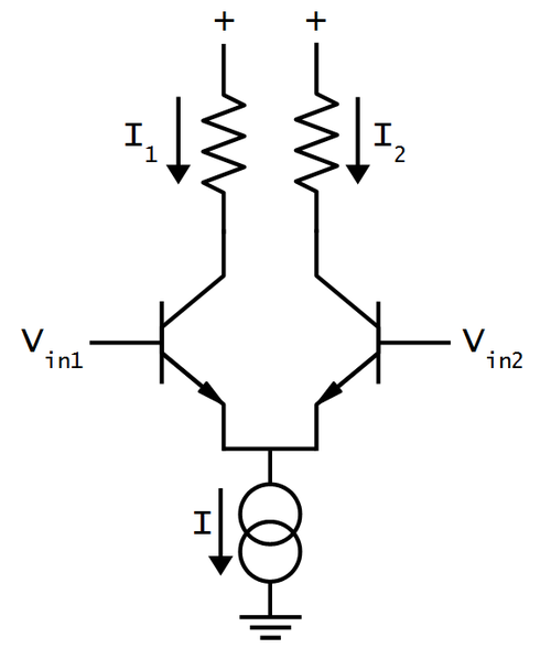
The second important circuit to understand is the differential pair, the most common two-transistor subcircuit used in analog ICs. 9 You may have wondered how a comparator compares two voltages, or an op amp subtracts two voltages. This is the job of the differential pair.

Schematic of a simple differential pair circuit. The current source sends a fixed current I through the differential pair. If the two inputs are equal, the current is split equally.

Schematic of a simple differential pair circuit. The current source sends a fixed current I through the differential pair. If the two inputs are equal, the current is split equally.

The schematic above shows a simple differential pair. The current source at the bottom provides a fixed current I, which is split between the two input transistors. If the input voltages are equal, the current will be split equally into the two branches (I1 and I2). If one of the input voltages is a bit higher than the other, the corresponding transistor will conduct exponentially more current, so one branch gets more current and the other branch gets less. A small input difference is enough to direct most of the current into the "winning" branch, flipping the comparator on or off. The 555 chip uses one differential pair for the threshold comparator and another for the trigger comparator.10

The 555 schematic interactive explorer

The 555 die photo and schematic11 below are interactive. Click on a component in the die or schematic, and a brief explanation of the component will be displayed. (For a thorough discussion of how the 555 timer works, see 555 Principles of Operation.)

For a quick overview, the large output transistors and discharge transistor are the most obvious features on the die. The threshold comparator consists of Q1 through Q8. The trigger comparator consists of Q10 through Q13, along with current mirror Q9. Q16 and Q17 form the flip flop. The three 5KΩ resistors forming the voltage divider are in the middle of the chip.12 Urban legend says that the 555 is named after these three 5K resistors, but according to its designer 555 is just an arbitrary number in the 500 chip series.

Click the die or schematic for details...

Conclusion

I hope you've found this look inside the 555 timer chip interesting. Next time you're building a 555 project, you'll know exactly what's inside the chip. I've written about the 555 timer before; this post is pretty much the same as that one but with a different die. I've also written about a CMOS version. Thanks to Eric Schlaepfer13 for providing the die; see his Twitter thread for background on this chip.

I announce my latest blog posts on Twitter, so follow me @kenshirriff and you won't miss an article! I also have an RSS feed.

Notes and references

  1. The 555 timer is iconic enough to appear on mugs, bags, caps and t-shirts. Whole books are devoted to 555 timer circuits

  2. The book Designing Analog Chips written by the 555's inventor Hans Camenzind is really interesting, and I recommend it if you want to know how analog chips work. Chapter 11 has an extensive discussion of the 555's history and operation. Page 11-3 claims the 555 has been the best-selling IC every year, although I don't know if that is still true. The free PDF is here or get the book

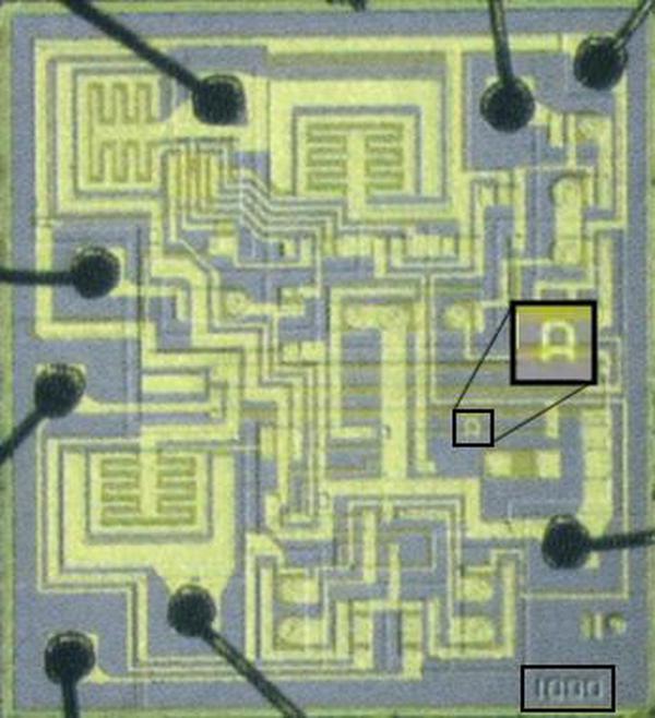
  3. The die has the part number 1000 and revision "C", so this probably corresponds to the 01003 number on the package. I suspect this chip is the third mask revision of the original 555.

    The first 555 die with the part number "1000" highlighted and the revision "A" magnified.

    The first 555 die with the part number "1000" highlighted and the revision "A" magnified.

    The die of the first 555 timer version (above) is marked with the number "1000" and revision "A". I compared this image with the die photo that I took and I couldn't see any differences except the revision changed to "C". The mask changes must have been fairly subtle. (This image is at Wikipedia and IEEE Spectrum. The image is captioned as the die shot of the first 555 timer IC manufactured in 1971.) 

  4. The 555 chip was introduced in mid-1972 according to Signetics Analog Applications page 149. 

  5. The brilliant part of the 555 timer is that the oscillation frequency depends only on the external resistors and capacitor and is insensitive to the supply voltage. If the supply voltage drops, the 1/3 and 2/3 references drop too, so you might expect the oscillations to be faster. But the lower voltage charges the capacitor more slowly, canceling this out and keeping the frequency constant.

    This voltage insensitivity is so tricky that the chip's designer didn't figure it out until near the end of the 555's design, but it made a big difference. The original design was more complex and required nine pins, which is a terrible size for an IC since there are no packages between 8 and 14 pins. The final, simpler 555 design worked with 8 pins, making the chip's packaging much cheaper. (See page 11-3 of Designing Analog Chips for the full story.) 

  6. You might have wondered why there is a distinction between the collector and emitter of a transistor, when the typical diagram of a transistor is symmetrical. As you can see from the die photo, the collector and emitter are very different in a real transistor. In addition to the very large size difference, the silicon doping is different. The result is a transistor will have poor gain if the collector and emitter are swapped. 

  7. For more information about current mirrors, check wikipedia, any analog IC book, or chapter 3 of Designing Analog Chips

  8. The schematic has the unusual symbol below, which indicates a transistor with two collectors. The base is drawn on the same side as the emitter and collectors, which adds to the confusion. On the die, this transistor is implemented with two separate transistors, with the emitters and the bases wired together. Other circuits sometimes use a single transistor that has two physical collectors present.

    This symbol indicates a transistor with two collectors.

    This symbol indicates a transistor with two collectors.


  9. Differential pairs are also called long-tailed pairs. According to Analysis and Design of Analog Integrated Circuits the differential pair is "perhaps the most widely used two-transistor subcircuits in monolithic analog circuits." (p214) For more information about differential pairs, see wikipedia, any analog IC book, or chapter 4 of Designing Analog Chips

  10. In the 555, the threshold comparator uses NPN transistors, while the trigger comparator uses PNP transistors. This allows the threshold comparator to work near the supply voltage and the trigger comparator to work near ground. The 555's comparators also use two transistors on each input (Darlington pair) to buffer the inputs. 

  11. The 555 schematic used in this article is from the Philips datasheet. It is identical to the Signetics schematic p150. 

  12. Note that the three resistors for the voltage divider are parallel and next to each other. This helps ensure they have the same resistance even if there are electrical variations across the silicon. 

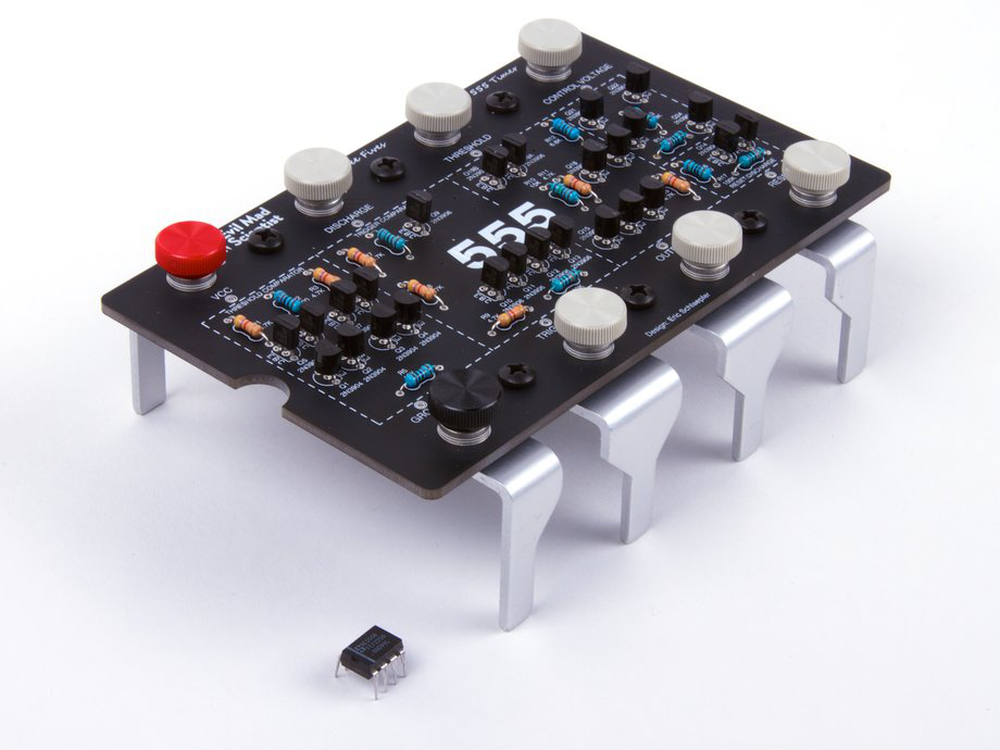
  13. Evil Mad Scientist sells a very cool discrete 555 timer kit, duplicating the 555 circuit on a larger scale with individual transistors and resistors — it actually works as a 555 replacement. Their 555 footstool is also worth a look.

    Large-size 555 timer created by Evil Mad Scientist Lab.

    Large-size 555 timer created by Evil Mad Scientist Lab.


Christmas shopping the IBM way: computerized gift selection in 1962

In 1962, the Simpson's department store in Toronto used an IBM computer to help customers select Christmas gifts, based on the characteristics of the recipients.1 I came across a video that shows how it worked.

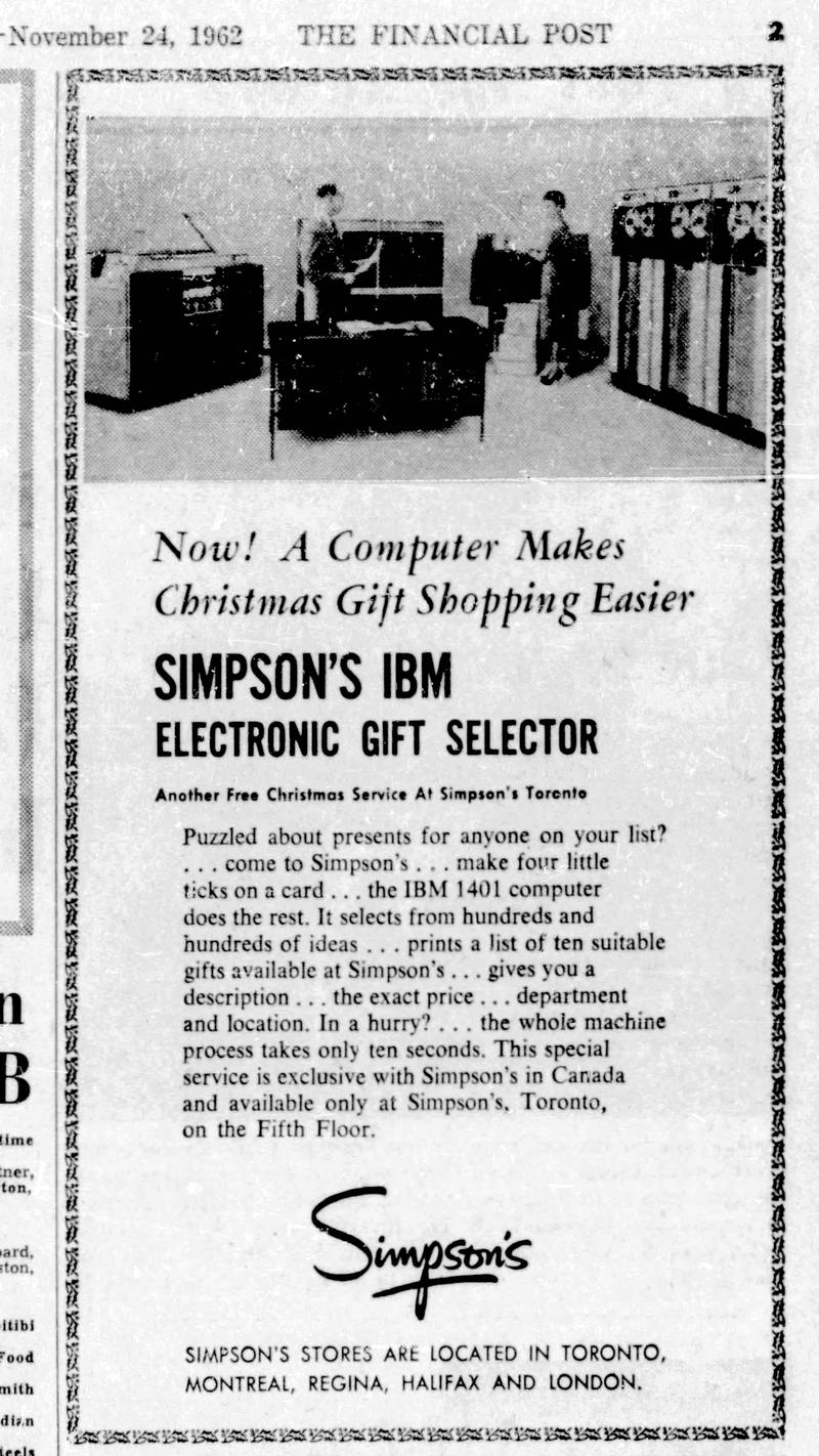
"Now! A computer makes Christmas shopping easier." The IBM 1401 computer is the cabinet at the back, with the 1403 printer to the right of it. The 1402 card reader is at the left and the 729 tape drives at the right, (Click for a larger version.) Advertisement in The Financial Post, November 24, 1962.

"Now! A computer makes Christmas shopping easier." The IBM 1401 computer is the cabinet at the back, with the 1403 printer to the right of it. The 1402 card reader is at the left and the 729 tape drives at the right, (Click for a larger version.) Advertisement in The Financial Post, November 24, 1962.

The IBM 1401 computer (below) was pre-programmed with 3000 categorized gifts.2 A customer described the gift recipient: their age range, their interests, their gender (male, female, or couple), the gift category (e.g. apparel, personal, or "the man who has everything"), and the price range (ranging from $5 to "money is no object").

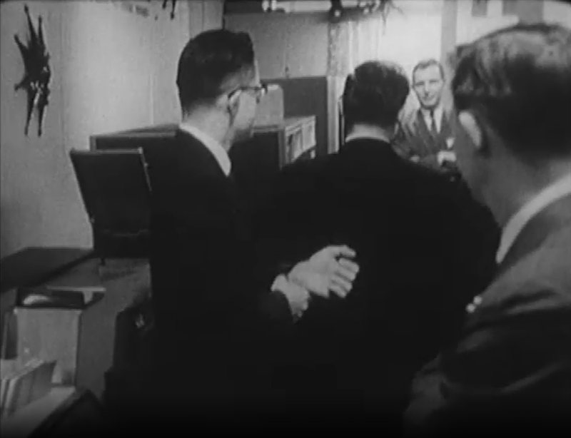
The IBM 1401 computer at Simpson's department store in 1962. The computer is barely visible behind the man's head. The 1402 card reader is at the left. Still from CBC video.

The IBM 1401 computer at Simpson's department store in 1962. The computer is barely visible behind the man's head. The 1402 card reader is at the left. Still from CBC video.

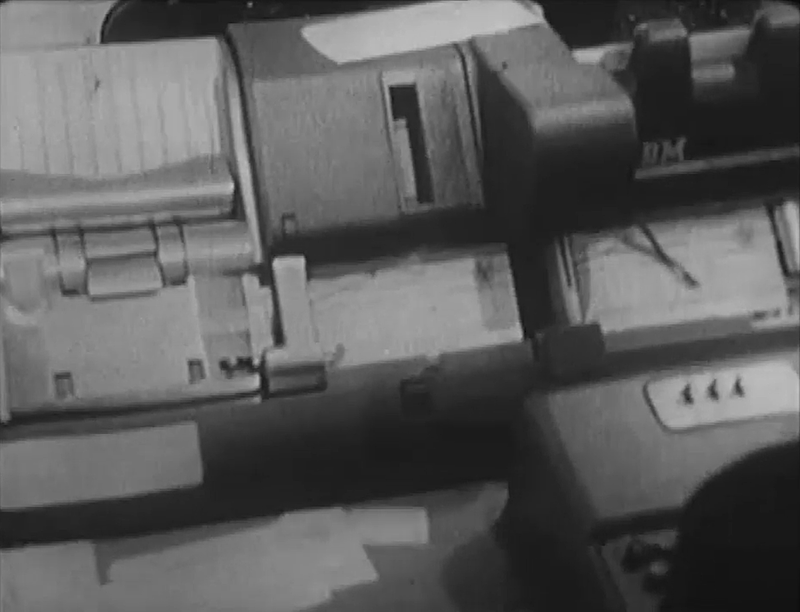
This information was punched onto a card by an operator (called a "girl" in the interview) using an IBM 26 keypunch, as shown below.

Entering the customer data into the IBM 26 keypunch. Still from CBC video.

Entering the customer data into the IBM 26 keypunch. Still from CBC video.

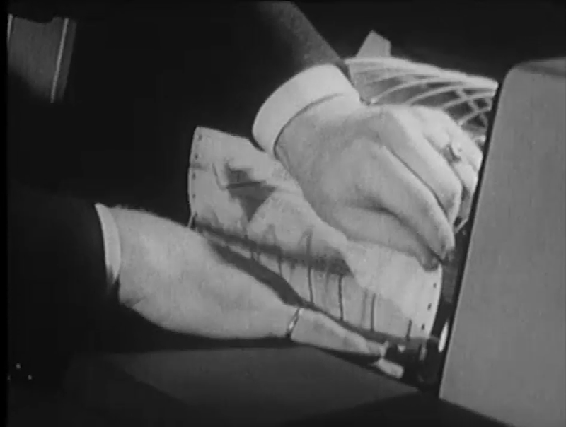
After running the card through the computer, a gift list with ten suggestions was printed on the IBM 1403 line printer. The list was torn off and given to the customer to help with their shopping.

Removing the Christmas shopping list from the IBM 1403 line printer. The Simpson's logo is barely visible in the upper left corner. Still from CBC video.

Removing the Christmas shopping list from the IBM 1403 line printer. The Simpson's logo is barely visible in the upper left corner. Still from CBC video.

The gift suggestions included a King James bible, Eskimo soapstone, a leather-covered cigarette case, Cossack boots, a Marabou-trim bed jacket, Roto-Shine electric shoe polisher ($26.95), a table lighter in the design of an antique pistol ($4.95), a soda siphon ($15.95) "a little more expensive, probably for your father or your husband", an electrified magnifying glass "to read the stock market report" ($7.95), or moccasins trimmed with seal fur ($6.95). (Gift ideas seem to have changed drastically since the 1960s.)

The interviewer suggested that this computer might take all the fun out of Christmas shopping and called it a "Santa monster", but the operator insisted that most people need some help with their shopping. It must have been an unusual experience for people to encounter a computer in person back then, but this gift computer was very popular, with 2000 people a day using it.

I announce my latest blog posts on Twitter, so follow me @kenshirriff. I also have an RSS feed. Thanks to Tim and Lisa Robinson for tracking down the newspaper clipping.

Notes and references

  1. The video is Christmas Shopping the IBM Way, broadcast on CBC on Dec 18, 1962. The host was Anna Cameron with guest Brian Finney. (Only the first part of the video shows the computer system; most of the video discusses the gift choices in detail.) The system was also discussed in a CBC Radio segment, Christmas Computer Selects the Perfect Gift, reported by Jim McLean and Joelle Pearson on Dec 4, 1962. The radio interview also discusses the use of the system at Gimbel's department store in New York. 

  2. The IBM 1401 computer is just barely visible in the video, so here's a photo that shows an IBM 1401 computer more clearly.

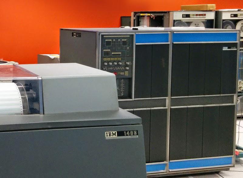
    An IBM 1401 computer. The line printer (1403) is in the foreground, while IBM 729 tape drives are in the background. This computer is at the Computer History Museum.

    An IBM 1401 computer. The line printer (1403) is in the foreground, while IBM 729 tape drives are in the background. This computer is at the Computer History Museum.


Reverse-engineering a tiny 1980s chip that plays Christmas tunes

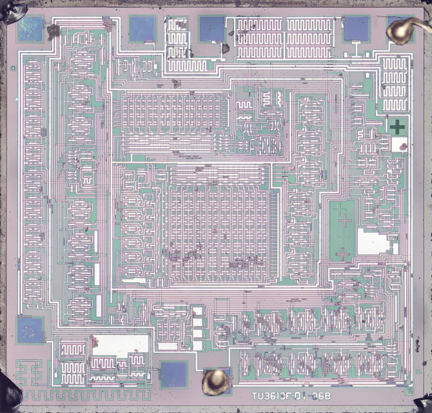
For the holidays, I decapped a chip that plays three Christmas melodies. The UM66T melody chip from the 1980s was designed for applications such as greeting cards and toys. It looks like a transistor, but when connected to a battery and speaker it plays music. The die photo below shows the tiny silicon chip that I reverse engineer in this blog post.

The UM66T die under the microscope. Click this (or any other) image for a larger version.

The UM66T die under the microscope. Click this (or any other) image for a larger version.

The video below shows the chip in action. Click to hear the chip play Jingle Bells, Santa Claus is Coming to Town, and We Wish You a Merry Christmas.

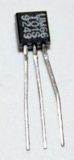
The chip is packaged in a 3-pin package that looks like a transistor (below). I dissolved the epoxy package in boiling sulfuric acid to expose the silicon die inside. This was my first acid decap and it turned out okay, although there are some scratches on the die. The composite photo above shows the CMOS chip under the microscope. The features are fairly large, even for the time; the metal traces are about 3.3µm wide and the silicon about 5.4µm.

The chip is in a 3-pin TO-92 package, like a transistor.

The chip is in a 3-pin TO-92 package, like a transistor.

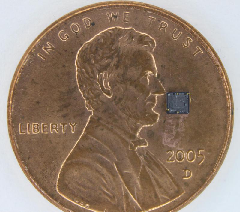
The silicon die is very small, about 1.8mm×1.8mm. The photo below gives an idea of the scale.

The UM66T die on top of a penny.

The UM66T die on top of a penny.

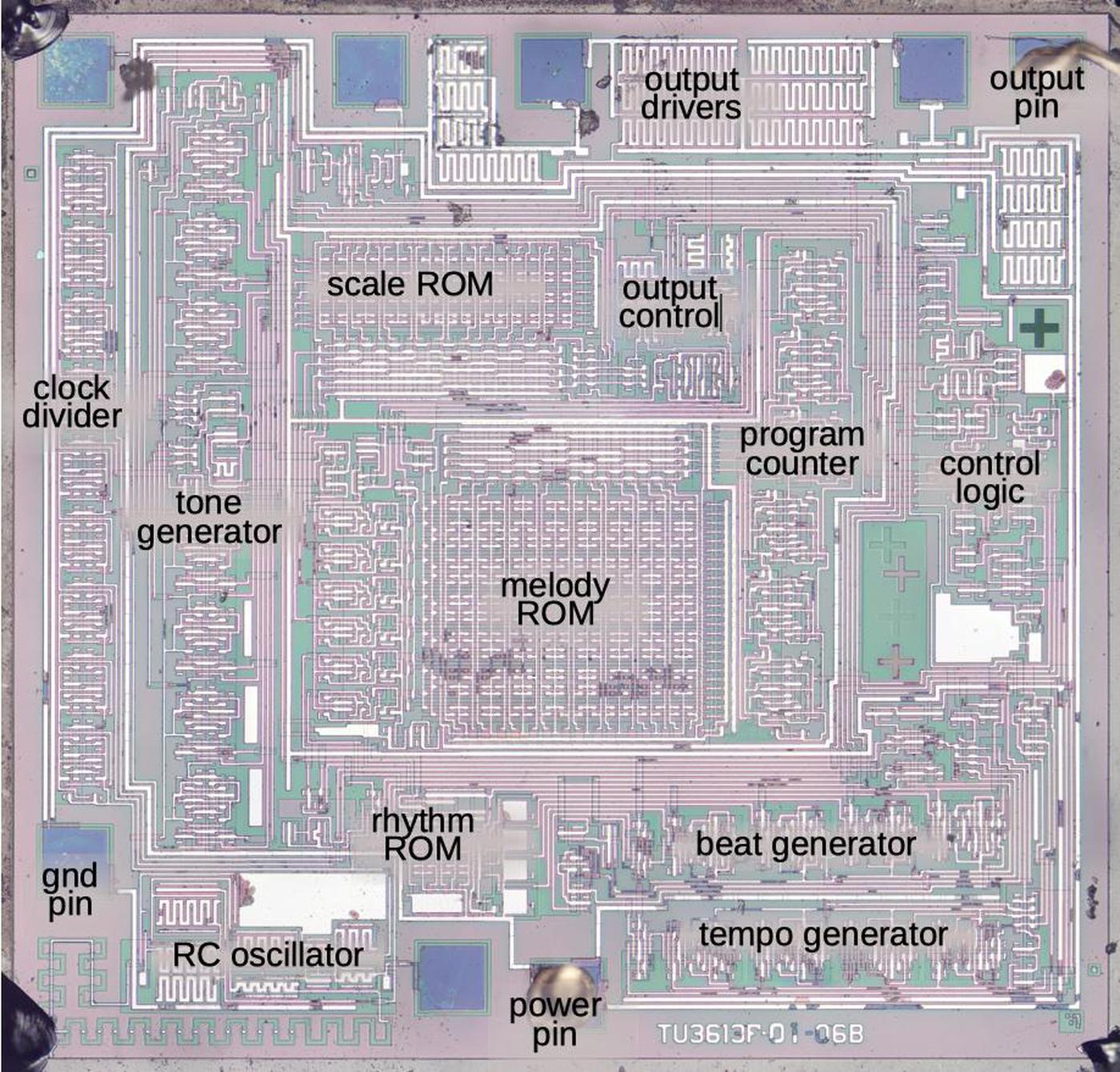
I've labeled the die photo with the functional blocks. The melody chip is an optimized, minimal design. It is constructed from flip-flops and gates, not the microcontroller you might expect.

Die photo of the UM66T with the main functional blocks labeled.

Die photo of the UM66T with the main functional blocks labeled.

The chip has 3 pins, but there are 8 pads on the die. The other pins appear to be used for testing. By activating one of the pins, the chip can be put into a test mode. The test mode runs through the songs at 512× speed so the chip can be tested quickly without waiting for the tunes to play. The other test pins appear to expose other internal data for testing.

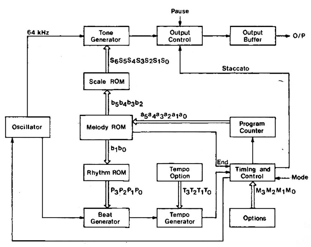
The block diagram below shows the structure of the chip. (Inconveniently, I didn't get this diagram until after I'd reverse-engineered the circuitry.) The basic idea is that the "program counter" steps through the 64 notes stored in the melody ROM. Four bits form the note pitch index, while two bits select the note duration. The Scale ROM and tone generator are used to convert the pitch index into the desired output tone. Meanwhile, the Rhythm ROM converts the 2-bit note duration into a 4-bit value indicating how long the note is.

Block diagram of the UM66T. From Maplin Magazine, March 1988.

Block diagram of the UM66T. From Maplin Magazine, March 1988.

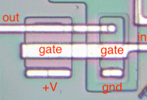
The chip is built from CMOS, like most modern ICs. The photo below shows an inverter: a PMOS transistor on the left and an NMOS transistor on the right. The PMOS one turns on with a 0 input, pulling the output high. The NMOS transistor turns on with a 1, pulling the output low. Thus, the two transistors implement the desired inverter behavior.

Structure of an inverter.

Structure of an inverter.

The melody ROM

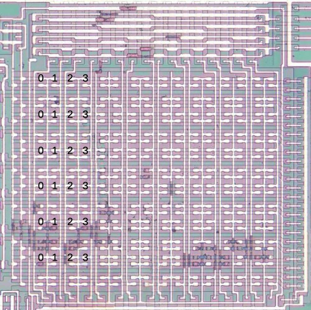
The 64 notes are stored in a 64×6 ROM, shown below. Each note is 4 bits for the frequency and 2 bits for the duration of the note. The ovals are the transistor gates; bits are stored in the wiring pattern of the transistors, either to the left or to the right. The vertical column select lines from the top select one column in the ROM. The vertical lines from the bottom, however, inactivate the transistor.

Physically, the ROM stores four notes in each column, so it has 16 columns of 24 bits. At the top of the ROM is a binary decoder that energizes one of the 16 columns, based on the input value. The transistors at the left of the ROM select one bit out of each four to produce the desired 6-bit word. The 6 bits are latched. Then 4 bits are used to generate the desired note frequency, while two bits select the duration of the note (half note, quarter note, or eighth note).

The melody ROM holds 64 notes.

The melody ROM holds 64 notes.

In the diagram above, the numbers show the locations of the first four words. The first word is 000100, a start code. The next two words are 011100; 0111 indicates the note E5 and 00 indicates a short duration.1 The next word is by 011101, indicating a longer E5. Thus, the indicated words store the first three notes of "Jingle Bells".

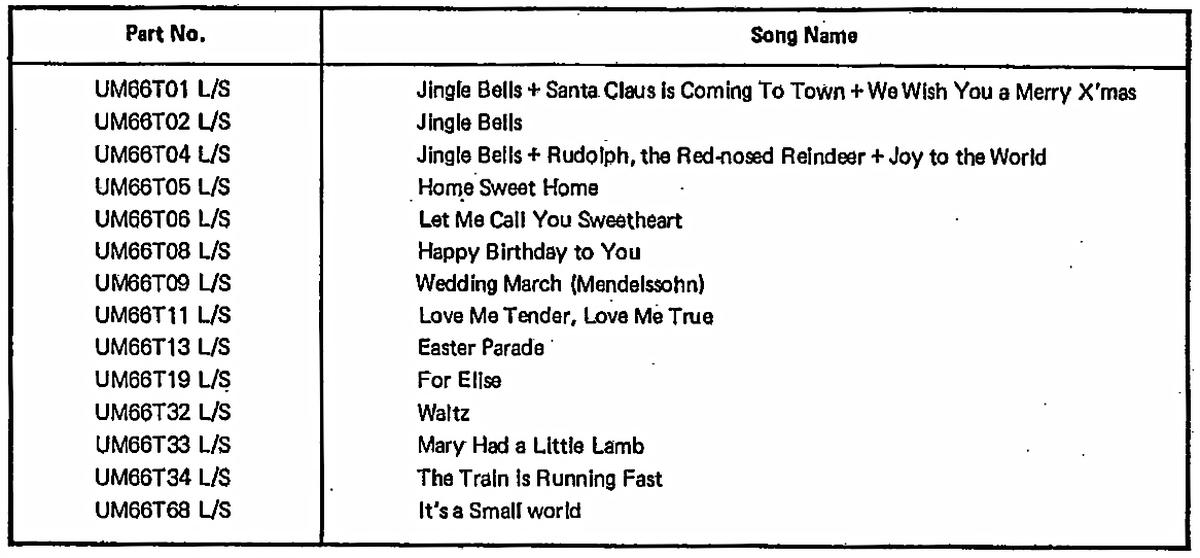
The metal layer of an IC can be changed relatively easily. By changing the metal layer, different versions of the chip could be manufactured with different ROMS, producing different songs. (The chip could also be manufactured with different note ranges, tempo, and beats, providing more flexibility.) The table below shows the songs that were available.2

List of songs available in the UM66T chip line. From the datasheet.

List of songs available in the UM66T chip line. From the datasheet.

Generating the note frequency

The melody ROM doesn't specify the note's frequency directly, but instead has a value from 0 to 15. A second ROM, the scale ROM, has the mapping to convert the note value into a frequency. Specifically, the output frequency is 32768÷N, where N is the value in the scale ROM. The frequency resolution from this isn't great, so some notes are noticeably out of tune, but it's good enough for this application.

The note frequency ROM.

The note frequency ROM.

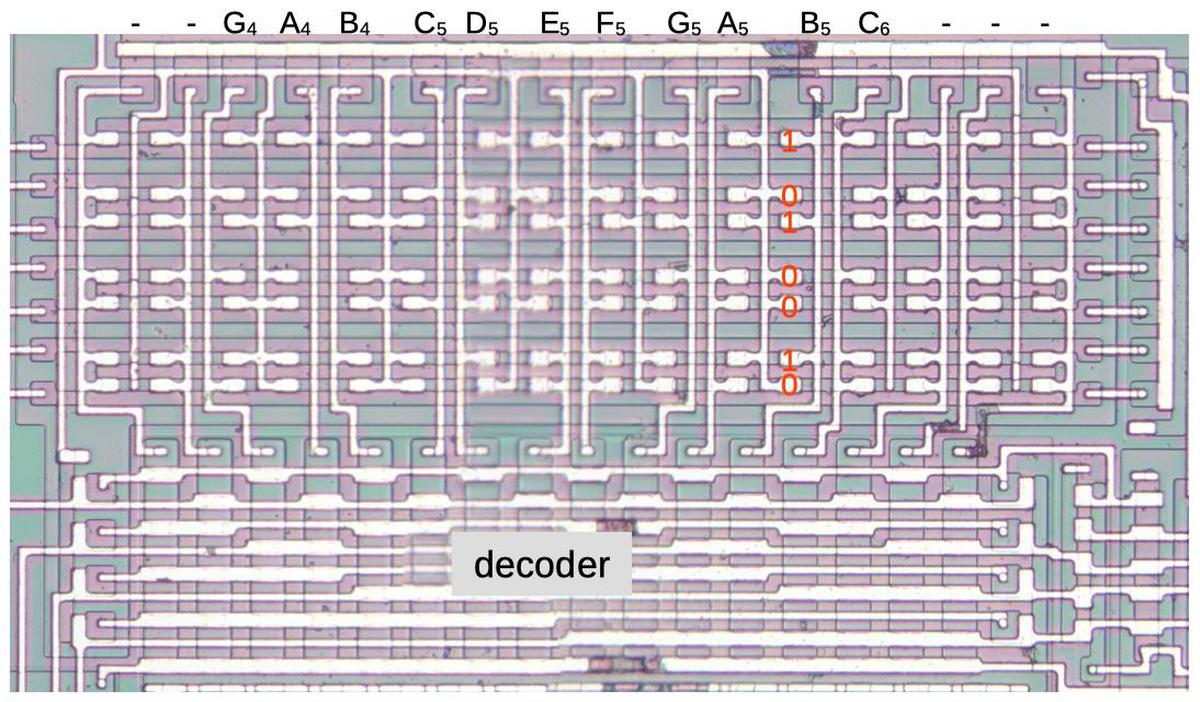
The image above shows the scale ROM, configured to produce the notes G4 through C6 in the key of C. (Different versions of the chip can generate different notes by changing the scale ROM.) As with the melody ROM, the binary values are generated by the wiring of the metal layer to the transistors. For instance, the note B5 has the bits 0,1,0,0,1,0,1 (from bottom to top). Below the ROM, the decoder activates one of the 16 column lines based on the 4-bit note value. (Notice the binary pattern of transistors in the decoder: the top rows alternate, the next rows are every 2, then every 4 and every 8.

The chip uses an unusual technique to generate the output frequency. The standard way is to divide the clock frequency by the scale factor with a counter, but instead the chip has an unusual approach to save a few transistors. It uses a 7-bit linear-feedback shift register. The construction of the linear-feedback shift register is that the input is the XOR of the last two bits. It will cycle pseudo-randomly through all 127 values.4

The trick in the melody chip is to initialize the shift register with a particular value loaded from the ROM, and run through the sequence until the value 1000000 is reached. By picking the right starting value, the desired number of counts will be obtained. The diagram below illustrates the operation of the shift register with the B5 input 0100101. With this starting value, it takes 34 steps to reach the final value of binary 1000000. Notice how the bits are shifted to the right each step, with a new bit inserted at the left.

0 1 0 0 1 0 1
1 0 1 0 0 1 0
1 1 0 1 0 0 1
1 1 1 0 1 0 0
0 1 1 1 0 1 0
1 0 1 1 1 0 1
1 1 0 1 1 1 0
1 1 1 0 1 1 1
0 1 1 1 0 1 1
0 0 1 1 1 0 1
1 0 0 1 1 1 0
1 1 0 0 1 1 1
0 1 1 0 0 1 1
0 0 1 1 0 0 1
1 0 0 1 1 0 0
0 1 0 0 1 1 0
1 0 1 0 0 1 1
0 1 0 1 0 0 1
1 0 1 0 1 0 0
0 1 0 1 0 1 0
1 0 1 0 1 0 1
1 1 0 1 0 1 0
1 1 1 0 1 0 1
1 1 1 1 0 1 0
1 1 1 1 1 0 1
1 1 1 1 1 1 0
1 1 1 1 1 1 1
0 1 1 1 1 1 1
0 0 1 1 1 1 1
0 0 0 1 1 1 1
0 0 0 0 1 1 1
0 0 0 0 0 1 1
0 0 0 0 0 0 1
1 0 0 0 0 0 0

Since this takes 34 steps, the clock frequency is divided by 34 and the output frequency is 32768 ÷ 34 = 963 Hertz, close to the desired frequency of 997 Hertz.3 For another example, G4 starts with 1001010 and runs for 84 counts, yielding a frequency of 392 Hertz. Thus, the ROM controls the frequency of the notes produced. Note that the starting values are not obviously correlated with the frequency; they depend on the sequence generated by the linear feedback shift register. (This sequence is called pseudo-random since it is deterministic but appears kind of random.)

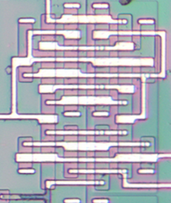
Next, I'll discuss the implementation of the shift register. The die photo below shows one stage of the shift register. It receives input from the stage below and passes its output to the stage above. The stage is constructed from 26 transistors: 13 PMOS transistors on the left and 13 NMOS transistors on the right. The transistors are oriented vertically along the pink regions of doped silicon. The transistor gates are where the metal lines widen. Note that transistors in a column are connected by the silicon.

Die photo showing one stage of the shift register.

Die photo showing one stage of the shift register.

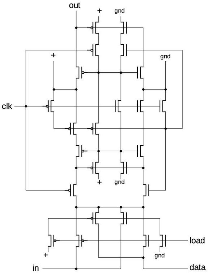
The schematic below shows how the transistors are connected, corresponding to the die photo above.

Schematic of one stage of the shift register, corresponding to the die photo.

Schematic of one stage of the shift register, corresponding to the die photo.

At a slightly higher level, the circuit consists of inverters and multiplexers5 as shown below. Each loop of two inverters holds a bit. The first multiplexer selects the input: either a value from the ROM that is loaded into the shift register, or the value from the previous stage. When the clock goes high, this value is loaded into the first inverter loop. When the clock goes low, the value in the first inverter loop is transferred to the second inverter loop, and thus the output. Thus, it takes one complete clock cycle (low then high) to shift a bit one stage in the shift register.

Schematic of one stage of the shift register.

Schematic of one stage of the shift register.

The clock

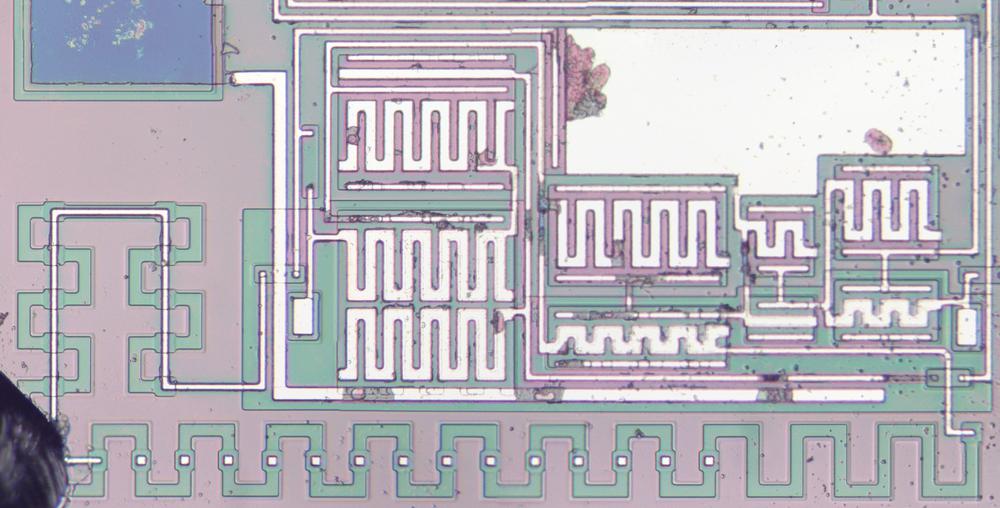
The chip runs on a 64-kilohertz clock. This clock is generated from a simple resistor-capacitor-inverter oscillator inside the chip, avoiding the need for external components. Because the capacitor takes some time to charge through the resistor, the oscillation speed is controlled.

The die photo below shows a closeup of the oscillator. The white rectangle is the capacitor. The green zig-zag is the resistor. Note that the resistance can be adjusted by shorting out part of the resistor in the metal layer. The white zig zags are the gates of the inverter transistors. These transistors are larger than the typical logic transistors.

Die photo showing the clock circuitry.

Die photo showing the clock circuitry.

The on-chip R-C oscillator is cheap but inaccurate, unlike a quartz crystal oscillator. If the voltage changes, the frequency changes. In the video below, I lower and raise the voltage, and you can hear the effect on the tunes as the frequency changes.

Timing

The 64-kilohertz clock goes through a divider chain to divide the frequency by 512. This divider is made of nine toggle flip-flops, each one dividing the frequency by 2. These flip-flops are built from inverters and multiplexers similar to the shift register flip-flops, but wired to toggle. This feeds the beat generator, which adjusts the timing for quarter notes, eighth notes, etc. It uses a linear-feedback shift register, similar to the tone generator, but with four shift register stages. The shift register is loaded with a value from the rhythm ROM that determines the length of the note.

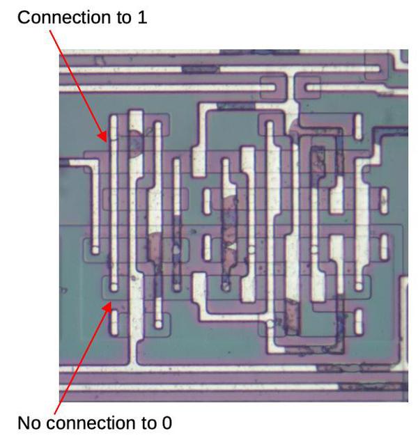
The output from the beat generator goes to the tempo generator, which divides its input by a preset amount (1 to 15) to generate a tempo between 128 and 1920 beats per minute. The tempo generator is also a 4-bit linear feedback shift register. The input to the shift register is hard wired to set the fixed tempo. The photo below shows one stage, wired to 1. A small change to the metal layer would cause 0 to be connected instead of 1.

The tempo is programmed by wiring shift register inputs to either 0 or 1.

The tempo is programmed by wiring shift register inputs to either 0 or 1.

The program counter counts through the 64 notes, providing the address to the melody ROM. It is built from toggle flip-flops chained together to build a 6-bit counter. The flip-flops have a reset line to initialize the counter to 0 at the start. The chip has a few dozen logic gates to keep track of the current state, handle startup, test mode, and so forth.

Conclusion

This melody chip uses simple circuits to produce songs in a flexible way. The chip integrates all the necessary circuitry including the R-C oscillator, so only a battery and a speaker were required. Nowadays a microcontroller would be the easiest way to implement this. This 1980s chip, however, uses small ROMS and simple counters to produce the tunes. I'll end with a quote from John Nolan: "Nothing says 'Christmas' like decapitating a microchip that plays slightly off-key Christmas songs."

This article is the extension of my earlier Twitter thread, which had a bunch of discussion on Hacker News. I announce my latest blog posts on Twitter, so follow me @kenshirriff. I also have an RSS feed. Thanks to Mark Fraser for finding an article on the chip.6

Notes and references

  1. The note codes range from 0010 for G4 through 1100 for C6, in the key of C. I wrote a short Python program to convert the ROM contents to notes. 

  2. Datasheets for the UM66T are available here, here, and here. A die photo of a different UM66T version is on siliconpr0n; I think this one plays Für Elise. 

  3. The output frequency is half what you might expect from the 64 kHz clock. To keep the waveform symmetrical, there is a toggle flip-flop on the output that divides the counter output by 2. 

  4. The 7-bit LFSR has 127 values instead of 128 values because it will get stuck in the all-zero value (since 0⊕0 = 0). 

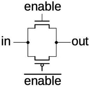
  5. The multiplexers are built from a CMOS circuit called a transmission gate (below). A transmission gate operates as a switch. When enable is high, both transistors turn on, passing the signal through the gate. When enable is low, both transistors turn off, blocking the signal. (Note that the PMOS transistor has an inverted control signal.) A multiplexer is built from two transmission gates. The control signal is connected to the two transmission gates with opposite polarity, so one transmission gate will be active at a time. Thus, one of the inputs is selected.

    Schematic of a transmission gate.

    Schematic of a transmission gate.


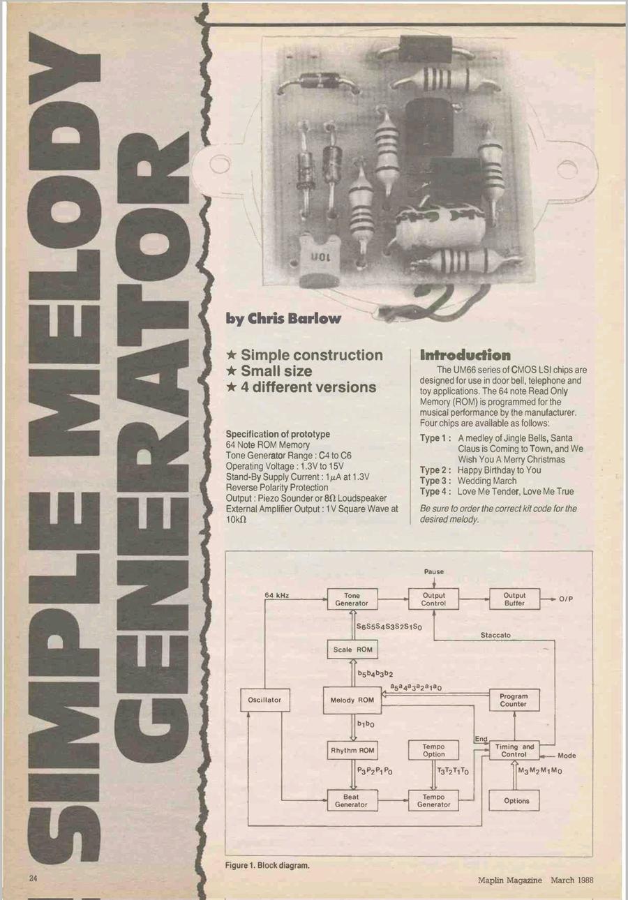
  6. A 1988 article (p24-26) in Maplin Electronics described how to build a circuit with the UM66T.

    First page of the article from Maplin Electronics, March 1988.

    First page of the article from Maplin Electronics, March 1988.