Inside the 74181 ALU chip: die photos and reverse engineering

What's inside a TTL chip? To find out, I opened up a 74181 ALU chip, took high-resolution die photos, and reverse-engineered the chip.1 Inside I found several types of gates, implemented with interesting circuitry and unusual transistors. The 74181 was a popular chip in the 1970s used to perform calculations in the arithmetic-logic unit (ALU) of minicomputers. It is a moderately complex chip containing about 67 gates and 170 transistors3, implemented using fast and popular TTL (transistor-transistor logic) circuitry.

The 74181 die photo is below. (Click the image for a high-resolution version.) The golden stripes are the metal layer that interconnects the circuitry of the chip. (It's not gold, just aluminum that looks golden from the lighting.) The white squares around the edge of the die are the pads that are connected by tiny bond wires to the external pins. Under the metal layer is the silicon that makes up the chip. Faint lines show the doped silicon regions that make up the transistors and resistors. While the chip may appear impossibly complex at first, with careful examination it is possible to understand how it works.

Die photo of the 74181 ALU chip.

Die photo of the 74181 ALU chip.

The 74181 chip is important because of its key role in minicomputer history. Before the microprocessor era, minicomputers built their processors from boards of individual chips. The arithmetic operations (addition, subtraction) and logical operations (AND, OR, XOR) were performed by the arithmetic/logic unit (ALU) in the processor. Early minicomputers built ALUs out of a large number of simple gates. But in March 1970, Texas Instruments introduced the 74181 Arithmetic / Logic Unit (ALU) chip, which put a full 4-bit ALU on one fast TTL chip.4 This chip provided 32 arithmetic5 and logic functions2, as well as fast carry lookahead.7 Using the 74181 chip simplified the design of a minicomputer processor and made it more compact, so it was used in many minicomputers. Computers using the 74181 ranged from the popular PDP-11 and NOVA minicomputers to the powerful VAX-11/780 to the Datapoint 2200 desktop computer. The 74181 is still used today in retro hacker projects.6

A brief guide to NPN transistors

The 74181 is built from bipolar NPN transistors, a different technology from the MOS transistors in modern processors. The diagram below shows how an NPN transistor appears in an integrated circuit, along with a cross section. The transistor has three connections: the collector, base and emitter, with metal lines for each. The collector is connected to N-type silicon, the base to P silicon, and the emitter to N silicon (giving it the NPN structure). On the chip, you can recognize the emitter from its nested squares, the base because its silicon region surrounds the emitter, and the collector because it is the largest contact.

Structure of an NPN transistor appears in an IC.

Structure of an NPN transistor appears in an IC.

The key idea of the NPN transistor is it acts as a switch between the collector and emitter, controlled by the base. Normally there is no current flow between the collector and the emitter, so it's like a switch in the "off" position. But if you pass a small current from base to emitter, the transistor allows a large current from collector to emitter, like a switch in the "on" position. (This is vastly oversimplified—bipolar transistors are much more "analog"—but should be enough to understand how the 74181 works.) At the right is the symbol for an NPN transistor with the collector, base and emitter labeled.

Inverter

The fundamental component of TTL logic is the inverter, and other gates are modifications of the inverter circuit. Thus, it's important to understand the basic construction of the inverter, even though it is a bit complicated. I'll explain how it works in an oversimplified way.9

The diagram below shows an inverter in the 74181 chip. The 5V and ground lines run vertically along the left, powering the inverter. The transistors are highlighted with boxes. The resistors are visible as long strips of doped silicon snaking around.11 An input pin (A0) is wired to the pad. On the right is the schematic for a TTL inverter10, with components highlighted to match the die photo.

An inverter in the 74181 ALU chip, along with a schematic showing the components of the inverter.

An inverter in the 74181 ALU chip, along with a schematic showing the components of the inverter.

The input is connected to transistor Q1 (red). This transistor is used in an unusual way, acting as a "current-steering" transistor. If the input is low, R1's current is steered through Q1's emitter to the input, leaving Q2 off. If the input is high, R1's current flows "backwards" out Q1's collector to Q2's base, turning on Q2. Transistor Q2 (orange) can be considered a "phase splitter transistor", which makes sure that exactly one of the output transistors (Q3 and Q4) is activated. (That is, they turn on in opposite phases.) If Q2 is off, R2 provides current to turn on Q3 (yellow), which pulls the output high. Meanwhile, R3 turns off Q4. On the other hand, if Q2 turns on, it provides enough current to turn on Q4 (green), which pulls the output low. I'll explain the diodes in a footnote.12

The 74181 schematic

The schematic below13 shows the circuitry of the 74181. If you've taken a digital logic course, you've probably seen how to build a full adder circuit. But if you look at the schematic of the 74181, it's implemented in a very different way, to provide higher speed and more flexibility.8 The main reason for its complexity is it computes everything in parallel, rather than waiting for the carry to ripple from bit to bit, and this requires a lot more logic.

The different types of gates are highlighted. There are a few inverters (red) to invert input signals. Most of the logic consists of AND-OR-INVERT gates. The AND stages are shown in blue, and the OR-INVERT (NOR) stages in green. (Some of the OR-INVERT stages are not explicit on the schematic and are empty boxes.) The chip uses a few XOR gates (purple) to compute sums. Finally, there are a couple unique gates shown in yellow.

Schematic of the 74181 ALU.

Schematic of the 74181 ALU.

The schematic can be matched up with the labeled die image below. Conveniently, the layout of the die largely matches the schematic. The AND-OR-INVERT gates make up the majority of the chip. Also notice the large chip real estate used for resistors. The chip pins are labeled with blue text. (The metal layer was removed for this photo, to make the underlying circuitry more visible.)

The 74181 ALU die, with main gate types outlined.

The 74181 ALU die, with main gate types outlined.

AND-OR-INVERT

Most of the 74181's logic is implemented with AND-OR-INVERT gates, which consist of AND gates connected to a NOR gate as shown below. After seeing the inverter, you may expect that an AND-OR-INVERT gate is very complex. But as the schematic below14 shows, the AND-OR-INVERT is not much more complex than an inverter, requiring just a few more transistors. An AND gate is implemented by adding more emitters to the current-steering input transistor (red). (This may seem very strange, but transistors with multiple emitters are common in TTL circuits.) If all inputs are high, the base current will be steered to the collector. Otherwise, the base current will flow out the emitter. Thus, the AND of the inputs is generated. The NOR gate is implemented by putting phase splitter transistors in parallel (orange). If any of the bases are high, the corresponding transistor (Q2A or Q2B) will conduct, pulling the output low. While the circuit below has two AND gates, it can easily be extended to as many gates and inputs as desired.

The AND-OR-INVERT circuit from the 7451 chip. The multiple-emitter transistors that implement AND are highlighted in red. The transistors that implement OR are highlighted in orange.

The AND-OR-INVERT circuit from the 7451 chip. The multiple-emitter transistors that implement AND are highlighted in red. The transistors that implement OR are highlighted in orange.

The diagram below shows how these multiple-emitter transistors are implemented on the chip. Three of these transistors are shown, each with four or five emitters (the dark squares), creating 4-input or 5-input AND gates. Each transistor's base is at the top and each collector is at the bottom. The signal lines run horizontally, with emitters connected as needed. With this structure, multiple AND gates can arranged efficiently on the chip (similar to a Programmable Logic Array or PLA). Note that the base resistors take up a significant amount of space.

Three AND gates in the 74181 ALU chip. Each one is a single transistor with multiple emitters.

Three AND gates in the 74181 ALU chip. Each one is a single transistor with multiple emitters.

The diagram below shows how the OR-INVERT part of the circuit appears on the chip. Note that Q2A and Q2B (orange) share a collector, so the two transistors don't take up much space on the die. Their inputs come from AND circuits such as the ones above. 3-input and 4-input OR gates are implemented similarly, by adding more transistors.

The OR-INVERT stage of the AND-OR-INVERT gate in the 74181, compared with the 7451 AND-OR-INVERT gate.

The OR-INVERT stage of the AND-OR-INVERT gate in the 74181, compared with the 7451 AND-OR-INVERT gate.

Exclusive-OR

The chip uses a clever, compact circuit to compute XOR with two transistors wired in an unusual way: the emitters and bases are tied together and there is no connection to ground. The way it works is if the first input is high and the second is low, the first transistor turns on due to the base-emitter current. This pulls the output low through the transistor, with the second input acting as ground. Likewise, if the first input is low and the second is high, the second transistor turns on and pulls the output low. If both inputs are the same, there is no base-emitter current, both transistors remain off, and the output is pulled high by the resistor. The output from the transistor pair goes to the standard inverter stage, so the resulting signal is the XOR of the two inputs. 15 As with OR-INVERT, the two transistors share a collector, making the layout more compact.

The circuit used in the 74181 to compute XOR. Layout inspired by userbinator.

The circuit used in the 74181 to compute XOR. Layout inspired by userbinator.

A few things to note about the photo. The two transistors share a collector, which is equivalent to wiring their collectors together. The pull-up resistor doesn't appear in the photo; it is off to the right. The inputs to the XOR are from AND-OR-INVERT gates; their output transistors are at the top of the photo.

NOT-AND

The chip uses four AND gates that have one inverted input.17 On the die, it appears at first that the gates are implemented with the standard AND transistors, but an interesting trick is used to invert one of the inputs. Transistor Q1 is wired in the normal current-steering way, with R1 providing a base current. But transistor Q2 has its resistor connected to the collector, not the base.16 Normally R2 will pull the output high. But if input X is high and input Y is low, R1's current will go through Q1's collector and Q2's emitter, turning on Q2 and pulling the output low. Thus, the result after the inverter stage will be X AND NOT Y.

The 74181 uses an interesting circuit to generate NOT-AND. It uses the multi-emitter transistors but in a subtly different way from the AND gates.

The 74181 uses an interesting circuit to generate NOT-AND. It uses the multi-emitter transistors but in a subtly different way from the AND gates.

Getting the die photos

To create die photos, the integrated circuit package must be opened to expose the silicon die inside. Most chips have an epoxy package, which can be dissolved in boiling sulfuric acid. Since I don't like boiling acid, I obtained the 74181 chip in a ceramic package, which is much easier to open.

The 74181 ALU chip in a ceramic package.

The 74181 ALU chip in a ceramic package.

I tapped the chip along the seam with a chisel, splitting the two layers apart. Below, you can see how the metal pins are mounted between the layers, and are connected to the silicon die with tiny bond wires.

By tapping the 74181 chip with a chisel, the ceramic package can be popped open.

By tapping the 74181 chip with a chisel, the ceramic package can be popped open.

To photograph the die, I used a metallurgical microscope, a special type of microscope that shines light down through the lens to illuminate the chip from above. I took 22 photographs and then used the Hugin stitching software to combine them into a high-resolution image (details). Then, I removed the metal layer from the chip with hydrochloric acid and took more images, resulting in the image below. Removing the metal makes it easier to see the structure of the silicon layer and determine how the chip works. (Click for high-resolution version.)

Removing the metal layer of the 74181 chip with HCl reveals the silicon layer underneath.

Removing the metal layer of the 74181 chip with HCl reveals the silicon layer underneath.

Conclusion

The 74181 ALU chip is a complex, high-performance TTL chip that was a key component in the processor of many minicomputers. I took detailed die photos of the 74181 ALU that reveal how the chip works internally. It uses several different logic gates, primarily AND-OR-INVERT gates that have an efficient layout on the chip. These gates are implemented by extending an inverter circuit in different ways, but are more complex than their MOS equivalents. I plan to explain how the 74181 implements its 32 functions and fast carry in a future article, so keep watching.

I announce my latest blog posts on Twitter, so follow me at kenshirriff. I also have an RSS feed.

Notes and references

  1. To understand what's inside a TTL chip, it might be more sensible to start with a simple chip such as a NAND gate. But why take the easy way when there's a complex chip to explore? 

  2. Many of the 74181's 32 functions are strange, but there is actually a system behind it. Note that there are exactly 16 possible functions on two (one-bit) binary inputs A and B. (There are 4 lines in the truth table, and two choices for each output, so 2^4 possible functions.) The 74181's 16 logic functions are simply these 16 functions (extended to 4 bits). The 74181's 16 arithmetic functions are A PLUS (one of the 16 possible functions of A and B) PLUS carry-in. 

  3. Various sources say the 74181 has 61 or 75 gates. The schematic shows 67 gates. If you omit the five 1-input AND gates, you get 62 gates, i. On the die, I counted 169 transistors, but it's quite possible I missed some. 

  4. The history of the 74181 chip is described in detail on this site. The 74181 is apparently the first ALU chip created. In 1968, Fairchild introduced the 3800, an 8-bit accumulator chip, but it didn't have logical functions so technically it's just an AU (Arithmetic Unit) not an ALU like the 74181. Before the 74181 was the 7483 4-bit adder chip (1968); internally, the 7483 is similar to the lower half of the 74181. The 7483 was used in minicomputers such as the PDP 8/E. 

  5. ALU chips of this era didn't perform multiplication or division, let alone floating point operations. Multiplication and division operations were common in computers of that era, but were typically performed with multiple cycles of addition or subtraction. The one operation that seems missing from the 74181 is "shift right"; it can do a shift left with "A PLUS A". 

  6. Retro projects using the 74181 include the APOLLO181 CPU, Fourbit CPU, 4 Bit TTL CPU, Magic-1 (using the 74F381), TREX, Mark 1 FORTH and Big Mess o' Wires

  7. When multiple 74181 chips are connected together for larger words, you can simply feed the carry-out of one chip into the carry-in of the next. For higher performance, the 74182 look-ahead carry generator could be used to compute the carries across multiple chips in parallel. Some minicomputers (such as the Xerox Alto) didn't use the 74182, while others (such as the Interdata 7/16) did. 

  8. I'll give a brief overview of the chip's implementation here. The chip is build around the idea of carry lookahead. In particular, the upper and-or-invert gates create the carry P (propagate) and G (generate) signals for each bit of A PLUS f(A,B). The lower and-or-invert gates use these signals to compute the carry for each bit of the sum. Finally, the xor gates add the P, G and carry to compute each final sum. The point of this implementation is to compute the four bits in parallel and avoid a slow ripple carry. In a later post I'll explain this circuitry in full detail. 

  9. I've simplified the discussion of the TTL logic circuit, since most people probably don't care about saturation, β, biasing, and so forth. If you want the full analysis, see Logic gates: the NOT gate or Transistor-Transistor Logic. This presentation shows schematics for the different gates and TTL logic families. 

  10. The inverter schematic is from the datasheet of the common 7404 inverter chip. Interestingly, the basic circuit used in an inverter chip is almost identical to the circuit used inside the 74181. This turns out to be true for most of the 74181 circuits—they are similar to individual TTL parts. The 74181's transistors are a bit smaller because not as much current is required inside the chip, but there is much less scaling than you might expect. 

  11. In the 74181's inverter, R4 is not used. R1 takes its place. This is probably because an inverter in the chip doesn't need to provide as much current as a 7404 inverter chip. 

  12. The tricky part of the inverter circuit is that if Q2 turns on, there's enough voltage to turn on Q4 but not Q3, thanks to diode D2. The purpose of diode D2 isn't to conduct current in one direction, like you'd expect from a diode. Instead, its purpose is to raise Q3's emitter voltage by one diode drop (about 0.7V). As a consequence, Q3 requires 0.7V more at the base to turn on. Thus, when Q2 is active, there is enough voltage to turn Q4 on, but not Q3. And diode D1 simply protects the chip by shunting any negative input voltage to ground. 

  13. The schematic is based on a diagram by Poil on WikiMedia, CC By-SA 3.0, with labeling changes and gates highlighted. 

  14. The AND-OR-INVERT schematic is slightly modified from the 7451 AND-OR-INVERT chip to match the 74181's circuit. The 74181's AND-OR-INVERT circuits in the lower half of the chip omit the pull-up output transistor found in the 7451 since the 74181 doesn't require as much output current internally. (The output diode remains to drop the phase splitter transistor's collector voltage by one diode drop, or else the low output voltage will be too high.) 

  15. The circuit used in the 74181 for exclusive-OR is similar to the 7486 TTL XOR chip

  16. On the die, Q2 appears to have two collectors. But these are just two contacts to the same collector, to simplify routing of the wiring. This is unlike the multiple-emitter transistors, which genuinely have multiple emitters. 

  17. Some datasheets (example) show an XOR gate instead of NOT-AND. You might wonder how this could possibly work since XOR and NOT-AND are different. The answer is that one of the four input combinations never happens in the 74181, and the gates are equivalent across the other three inputs. The physical implementation is NOT-AND rather than XOR. 

Die photos and analysis of the revolutionary 8008 microprocessor, 45 years old

Intel's groundbreaking 8008 microprocessor was first produced 45 years ago.1 This chip, Intel's first 8-bit microprocessor, is the ancestor of the x86 processor family that you may be using right now. I couldn't find good die photos of the 8008, so I opened one up and took some detailed photographs. These new die photos are in this article, along with a discussion of the 8008's internal design.

Die photograph of the 8008 microprocessor

Die photograph of the 8008 microprocessor

The photo above shows the tiny silicon die inside the 8008 package. (Click the image for a higher resolution photo.) You can barely see the wires and transistors that make up the chip. The squares around the outside are the 18 pads that are connected to the external pins by tiny bond wires. You can see the text "8008" on the right edge of the chip and "© Intel 1971" on the lower edge. The initials HF appear on the top right for Hal Feeney, who did the chip's logic design and physical layout. (Other key designers of the 8008 were Ted Hoff, Stan Mazor, and Federico Faggin.)

Inside the chip

The diagram below highlights some of the major functional blocks of the chip. On the left is the 8-bit Arithmetic/Logic Unit (ALU), which performs the actual data computations.3 The ALU uses two temporary registers to hold its input values. These registers take up significant area on the chip, not because they are complex, but because they need large transistors to drive signals through the ALU circuitry.

Die of the 8008 microprocessor showing major components.

Die of the 8008 microprocessor showing major components.

Below the registers is the carry look ahead circuitry. For addition and subtraction, this circuit computes all eight carry values in parallel to improve performance.2 Since the low-order carry depends on just the low-order bits, while the higher-order carries depend on multiple bits, the circuit block has a triangular shape.

The triangular layout of the ALU is unusual. Most processors stack the circuitry for each bit into a regular rectangle (a bit-slice layout). The 8008, however, has eight blocks (one for each bit) arranged haphazardly to fit around the space left by the triangular carry generator. The ALU supports eight simple operations.3

In the center of the chip is the instruction register and the instruction decoding logic that determines the meaning of each 8-bit machine instruction. Decoding is done with a Programmable Logic Array (PLA), an arrangement of gates that matches bit patterns and generates the appropriate control signals for the rest of the chip. On the right are the storage blocks. The 8008's seven registers are in the upper right. In the lower right is the address stack, which consists of eight 14-bit address words. Unlike most processors, the 8008's call stack is stored on the chip instead of in memory. The program counter is just one of these addresses, making subroutine calls and returns very simple. The 8008 uses dynamic memory for this storage

The physical structure of the chip is very close to the block diagram in the 8008 User's Manual (below), with blocks located on the chip in nearly the same positions as in the block diagram.

Block diagram of the 8008 microprocessor, from the User's Manual.

Block diagram of the 8008 microprocessor, from the User's Manual.

The structure of the chip

What does the die photo show? For our purposes, the chip can be thought of as three layers. The diagram below shows a closeup of the chip, pointing out these layers. The topmost layer is the metal wiring. It is the most visible feature, and looks metallic (not surprisingly). In the detail below, these wires are mostly horizontal. The polysilicon layer is below the metal and appears orange under the microscope.

A closeup of the 8008 die, showing the metal layer, the polysilicon, and the doped silicon.

A closeup of the 8008 die, showing the metal layer, the polysilicon, and the doped silicon.

The foundation of the chip is the silicon wafer, which appears purplish-gray in the photo. Pure silicon is effectively an insulator. Regions of it are "doped" with impurities to create semiconducting silicon. Being on the bottom, the silicon layer is difficult to distinguish, but you can see black lines along the border between doped silicon and undoped silicon. A few vertical silicon "wires" are visible in the photo.4

Transistors are the key component of the chip, and a transistor is formed where a polysilicon wire crosses doped silicon. In the photo, the polysilicon appears as a brighter orange where it forms a transistor.

Why an 18 pin chip?

One inconvenient feature of the 8008 is it only has 18 pins, which makes the chip slower and much more difficult to use. The 8008 uses 14 address bits and 8 data bits so with 18 pins there aren't enough pins for each signal. Instead, the chip has 8 data pins that are reused in three cycles to transmit the low address bits, high address bits, and data bits. A computer using the 8008 requires many support chips to interact with this inconvenient bus architecture.5

There was no good reason to force the chip into 18 pins. Packages with 40 or 48 pins were common with other manufacturers, but 16 pins was "a religion at Intel".6 Only with great reluctance did they move to 18 pins. By the time the 8080 processor came out a few years later, Intel had come to terms with 40-pin chips. The 8080 was much more popular, in part because it had a simpler bus design permitted by the 40-pin package.

Power and data paths in the chip

The data bus provides data flow through the chip. The diagram below shows the 8-bit data bus of the 8008 with rainbow colors for the 8 data lines. The data bus connects to the 8 data pins along the outside of the upper half of the chip. The bus runs between the ALU on the left, the instruction register (upper center), and the registers and stack on the right. The bus is split on the left with half along each side of the ALU.

Die photo of the 8008 microprocessor. The power bus is shown in red and blue. The data bus is shown with 8 rainbow colors.

Die photo of the 8008 microprocessor. The power bus is shown in red and blue. The data bus is shown with 8 rainbow colors.

The red and blue lines show power routing. Power routing is an under-appreciated aspect of microprocessors. Power is routed in the metal layer due to its low resistance. But since there is only one metal layer in early microprocessors, power distribution must be carefully planned so the paths don't cross.7 The diagram above shows Vcc lines in blue and Vdd lines in red. Power is supplied through the Vcc pin on the left and the Vdd pin on the right, then branches out into thin, interlocking wires that supply all parts of the chip.

The register file

To show what the chip looks like in detail, I've zoomed in on the 8008's register file in the photo below. The register file consists of an 8 by 7 grid of dynamic RAM (DRAM) storage cells, each using three transistors to hold one bit.8 (You can see the transistors as the small rectangles where the orange polysilicon takes on a slightly more vivid color.) Each row is one of the 8008's seven 8-bit registers (A, B, C, D, E, H, L). On the left, you can see seven pairs of horizontal wires: the read select and write select lines for each register. At the top, you can see eight vertical wires to read or write the contents of each bit, along with 5 thicker wires to supply Vcc. Using DRAM for registers (rather than the more common static latches) is an interesting choice. Since Intel was primary a memory company at the time, I expect they chose DRAM due to their expertise in the area.

The register file in the 8008. The chip has seven 8-bit registers: A, B, C, D, E, H, L

The register file in the 8008. The chip has seven 8-bit registers: A, B, C, D, E, H, L

How PMOS works

The 8008 uses PMOS transistors. To simplify slightly, you can think of a PMOS transistor as a switch between two silicon wires, controlled by a gate input (of polysilicon). The switch closes when its gate input is low and it can pull its output high. If you're familiar with the NMOS transistors used in microprocessors like the 6502, PMOS may be a bit confusing because everything is backwards.

A simple PMOS NAND gate can be constructed as shown below. When both inputs are high, the transistors are off and the resistor pulls the output low. When any input is low, the transistor will conduct, connecting the output to +5. Thus, the circuit implements a NAND gate. For compatibility with 5-volt TTL circuits, the PMOS gate (and thus the 8008) is powered with unusual voltages: -9V and +5V.

A NAND gate implemented with PMOS logic.

A NAND gate implemented with PMOS logic.

For technical reasons, the resistor is actually implemented with a transistor. The diagram below shows how the transistor is wired to act as a pull-down resistor. The detail on the right shows how this circuit appears on the chip. The -9V metal wire is at the top, the transistor is in the middle, and the output is the silicon wire at the bottom.

In PMOS, a pull-down resistor (left) is implemented with a transistor (center). The photo on the right shows an actual pull-down in the 8008 microprocessor.

In PMOS, a pull-down resistor (left) is implemented with a transistor (center). The photo on the right shows an actual pull-down in the 8008 microprocessor.

History of the 8008

The 8008's complicated story starts with the Datapoint 2200, a popular computer introduced in 1970 as a programmable terminal. (Some people consider the Datapoint 2200 to be the first personal computer.) Rather than using a microprocessor, the Datapoint 2200 contained a board-sized CPU build from individual TTL chips. (This was the standard way to build a CPU in the minicomputer era.) Datapoint and Intel decided that it would be possible to replace this board with a single MOS chip, and Intel started the 8008 project to build this chip. A bit later, Texas Instruments also agreed to build a single-chip processor for Datapoint. Both chips were designed to be compatible with the Datapoint 2200's 8-bit instruction set and architecture.

The 8008 processor was first described publicly in "Electronic Design", Oct 25, 1970. Although Intel claimed the chip would be delivered in January 1971, actual delivery was more than a year later in April, 1972.

The 8008 processor was first described publicly in "Electronic Design", Oct 25, 1970. Although Intel claimed the chip would be delivered in January 1971, actual delivery was more than a year later in April, 1972.

Around March 1971, Texas Instruments completed their processor chip, calling it the TMC 1795. After delaying the project, Intel finished the 8008 chip later, around the end of 1971. For a variety of reasons, Datapoint rejected both microprocessors and built a faster CPU based on newer TTL chips including the 74181 ALU chip. TI tried unsuccessfully to market the TMC 1795 processor to companies such as Ford, but ended up abandoning the processor, focusing on highly-profitable calculator chips instead. Intel, on the other hand, marketed the 8008 as a general-purpose microprocessor, which eventually led to the x86 architecture you're probably using right now. Although TI was first with the 8-bit processor, it was Intel who made their chip a success, creating the microprocessor industry.

A family tree of the 8008 and some related processors. Black arrows indicate backwards compatibility. Light arrows indicate significant architecture changes.

A family tree of the 8008 and some related processors. Black arrows indicate backwards compatibility. Light arrows indicate significant architecture changes.

The diagram above summarizes the "family tree" of the 8008 and some related processors.10 The Datapoint 2200's architecture was used in the TMC 1795, the Intel 8008, and the next version Datapoint 220011. Thus, four entirely different processors were built using the Datapoint 2200's instruction set and architecture. The Intel 8080 processor was a much-improved version of the 8008. It significantly extended the 8008's instruction set and reordered the machine code instructions for efficiency. The 8080 was used in groundbreaking early microcomputers such as the Altair and the Imsai. After working on the 4004 and 8080, designers Federico Faggin and Masatoshi Shima left Intel to build the Zilog Z-80 microprocessor, which improved on the 8080 and became very popular.

The jump to the 16-bit 8086 processor was much less evolutionary. Most 8080 assembly code could be converted to run on the 8086, but not trivially, as the instruction set and architecture were radically changed. Nonetheless, some characteristics of the Datapoint 2200 still exist in today's x86 processors. For instance, the Datapoint 2200 had a serial processor, processing bytes one bit at a time. Since the lowest bit needs to be processed first, the Datapoint 2200 was little-endian. For compatibility, the 8008 was little-endian, and this is still the case in Intel's processors. Another feature of the Datapoint 2200 was the parity flag, since parity calculation was important for a terminal's communication. The parity flag has continued to the x86 architecture.

The 8008 is architecturally unrelated to Intel's 4-bit 4004 processor12. The 8008 is not an 8-bit version of the 4-bit 4004 in any way. The similar names are purely a marketing invention; during its design phase the 8008 had the unexciting name "1201".

If you want more early microprocessor history, I wrote a detailed article for the IEEE Spectrum. I also wrote a post about TI's TMC 1795.

How the 8008 fits into the history of semiconductor technology

The 4004 and 8008 both used silicon-gate enhancement-mode PMOS, a semiconductor technology that was only used briefly. This puts the chips at an interesting point in chip fabrication technology.

The 8008 (and modern processors) uses MOS transistors. These transistors had a long path to acceptance, being slower and less reliable than the bipolar transistors used in most computers of the 1960s. By the late 1960s, MOS integrated circuits were becoming more common; the standard technology was PMOS transistors with metal gates. The gates of the transistor consisted of metal, which was also used to connect components of the chip. Chips essentially had two layers of functionality: the silicon itself, and the metal wiring on top. This technology was used in many Texas Instruments calculator chips, as well as the TMC 1795 chip (the chip that had the same instruction set as the 8008).

A key innovation that made the 8008 practical was the self-aligned gate—a transistor using a gate of polysilicon rather than metal. Although this technology was invented by Fairchild and Bell Labs, it was Intel that pushed the technology ahead. Polysilicon gate transistors had much better performance than metal gate (for complex semiconductor reasons). In addition, adding a polysilicon layer made routing of signals in the chip much easier, making the chips denser. The diagram below shows the benefit of self-aligned gates: the metal-gate TMC 1795 is bigger than the 4004 and 8008 chips combined.

Intel's 4004 and 8008 processors are much denser than Texas Instruments' TMC 1795 chip, largely due to their use of self-aligned gates.

Intel's 4004 and 8008 processors are much denser than Texas Instruments' TMC 1795 chip, largely due to their use of self-aligned gates. TMC 1795 die photo courtesy of Computer History Museum.

Shortly afterwards, semiconductor technology improved again with the use of NMOS transistors instead of PMOS transistors. Although PMOS transistors were easier to manufacture initially, NMOS transistors are faster, so once NMOS could be fabricated reliably, they were a clear win. NMOS led to more powerful chips such as the Intel 8080 and the Motorola 6800 (both 1974). Another technology improvement of this time was ion-implantation to change the characteristics of transistors. This allowed the creation of "depletion-mode" transistors for use as pull-up resistors. These transistors improved chip performance and reduced power consumption. They also allowed the creation of chips that ran on standard five-volt supplies.13 The combination of NMOS transistors and depletion-mode pull-ups was used for most of the microprocessors of the late 1970s and early 1980s, such as the 6502 (1975), Z-80 (1976), 68000 (1979), and Intel chips from the 8085 (1976) to the 80286 (1982).

In the mid 1980s, CMOS took over, using NMOS and PMOS transistors together to dramatically reduce power consumption, with chips such as the 80386 (1986), 68020 (1984) and ARM1 (1985). Now almost all chips are CMOS.14

As you can see, the 1970s were a time of large changes in semiconductor chip technology. The 4004 and 8008 were created when the technological capability intersected with the right market.

How to take die photos

In this section, I explain how I got the photos of the 8008 die. The first step is to open the chip package to expose the die. Most chips come in epoxy packages, which can be dissolved with dangerous acids.

The 8008 microprocessor in a ceramic package

The 8008 microprocessor in a ceramic package

Since I would rather avoid boiling nitric acid, I took a simpler approach. The 8008 is also available in a ceramic package (above), which I got on eBay. Tapping the chip along the seam with a chisel pops the two ceramic layers apart. The photo below shows the lower half of the ceramic package, with the die exposed. Most of the metal pins have been removed, but their positions in the package are visible. To the right of the die is a small square; this connects ground (Vcc) to the substrate. A couple of the tiny bond wires are still visible, connected to the die.

Inside the package of the 8008 microprocessor, the silicon die is visible.

Inside the package of the 8008 microprocessor, the silicon die is visible.

Once the die is exposed, a microscope can be used to take photographs. A standard microscope shines the light from below, which doesn't work well for die photographs. Instead, I used a metallurgical microscope, which shines the light from above to illuminate the chip.

I took 48 photographs through the microscope and then used the Hugin stitching software to combine them into one high-resolution image (details). Finally, I adjusted the image contrast to make the chip's structures more visible. The original image (which is approximately what you see through the microscope) is below for comparison.

Die photograph of the 8008 microprocessor

Die photograph of the 8008 microprocessor

Conclusion

I took detailed die photos of the 8008 that reveal the circuitry it used. While the 8008 wasn't the first microprocessor or even the first 8-bit microprocessor, it was truly revolutionary, triggering the microprocessor revolution and leading to the x86 architecture that dominates personal computers today. In future posts, I plan to explain the 8008's circuits in detail to provide a glimpse into the roots of todays computers.

I announce my latest blog posts on Twitter, so follow me at kenshirriff. Or you can use the RSS feed.

Notes and references

  1. According to the oral history of the 8008, photos of the 8008 were obtained in October / November 1971 (page 6). Chip designer Federico Faggin mentions that toward the end of 1971, "everything was working except for a few errors." Faggin then debugged a problem with the dynamic memory losing data, making it ready for production (page 9). 

  2. Using the carry look ahead circuit avoids the delay from a standard ripple-carry adder, where the carries propagate through the sum. 

  3. The 8008's ALU supports eight operations: add, subtract, add with carry, subtract with carry, AND, OR, XOR, and compare. It also implements left and right shift and rotate operations. The 8008 also has increment and decrement instructions, extending the Datapoint 2200's instruction set

  4. Because silicon has higher resistance than polysilicon, most chips use the polysilicon and metal layers for wiring, not the silicon layer. The 4004 and 8008 chips are unusual in that they prefer to use the silicon layer for wiring rather than polysilicon. I expect this was due to the recent introduction of polysilicon: before polysilicon, routing needed to be done in the silicon layer and perhaps the chip designers were sticking with the older layout techniques. 

  5. The 8008 required 20 support chips according to chip architect Federico Faggin. In contrast, the 4004 and earlier MOS computers such as the Four Phase and CADC were designed with a small number of MOS chips that worked together without extra "glue chips". In this sense, the 8008 was a step backwards architecturally, saying "here's the CPU, you figure out how to make a computer out of it." 

  6. For details on Intel's insistence on 16 pins, see Oral History of Federico Faggin, page 55-56. It was only when the 1103 memory chip required 18 pins that Intel reluctantly moved beyond 16 pins. And that was treated by Intel like "the sky had dropped from heaven," resulting in "so many long faces". 

  7. If two metal lines need to cross, one of them can be routed under the other by using the polysilicon layer. To be low resistance, this cross-under must be relatively wide, so cross-unders are avoided if possible. 

  8. The 8008 registers use the "3T1C" cell: three transistors and one capacitor (details). The circuit doesn't physically contain a separate capacitor, but uses the gate capacitance of the transistor. One unusual feature of the 8008 cell is it uses one wire for both reading and writing the bit, while the typical 3T cell has separate wires for reading and writing. The 4004 had separate wires, but the design changed slightly in the 8008. 

  9. Pull-up resistors in later chips such as the 6502 were implemented using depletion-mode NMOS transistors. These yielded more faster, more efficient logic. They were also wired differently, with the gate connected to the output rather than the power rail. 

  10. The 8008 architecture and the evolution of Intel's microprocessors are discussed in detail in Intel Microprocessors: 8008 to 8086

  11. The second version of the Datapoint 2200 had a totally new implementation of the processor, still built from TTL chips. While the first version had a serial ALU (processing one bit at a time), the second version operated in parallel using 74181 ALU chips. As a result, the second version was much faster. 

  12. The extensive 4004 Anniversary Project has reverse-engineered the 4004 processor. The 4004 schematic is here

  13. The Motorola 6800 microprocessor originally used enhancement-mode transistors. To operate off a single +5V supply, it had a voltage-doubler circuit on the chip. 

  14. Interestingly, in 2007 Intel started using metal gates again in order to scale transistors further (details). In a way, semiconductor technology has gone full circle, back to metal gates, although now unusual metals such as hafnium are used. 

Superbeta transistors inside: Die photos and analysis of the LM108 op amp

The LM108 op amp is an interesting chip to examine under a microscope because it uses special superbeta transistors for high performance. Photos of the die reveal the tiny circuitry of the chip as well as unused components that make the chip more complex than necessary. Surprisingly, these extra components allow the same die to be reused for two totally different chips! In this article I examine the internals of the LM108 in detail, explain how it works and reveal how the die can take on two roles.

I've written about the famous 741 op amp, which came out in 1968. A year later, the improved LM108 op amp was invented by eccentric analog IC design genius Bob Widlar.[1] The main claim to fame of the LM108 is it uses a very small input current, orders of magnitude smaller than the 741.[2] To attain this low input current, the LM108 contains special transistors called "superbeta" transistors, with about 25 times the amplification of a regular transistor.[3] The downside is the superbeta transistors are delicate and require special circuitry to protect them from damage.

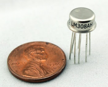
The LM308 op amp in an 8-pin metal can.

The LM308 op amp in an 8-pin metal can.

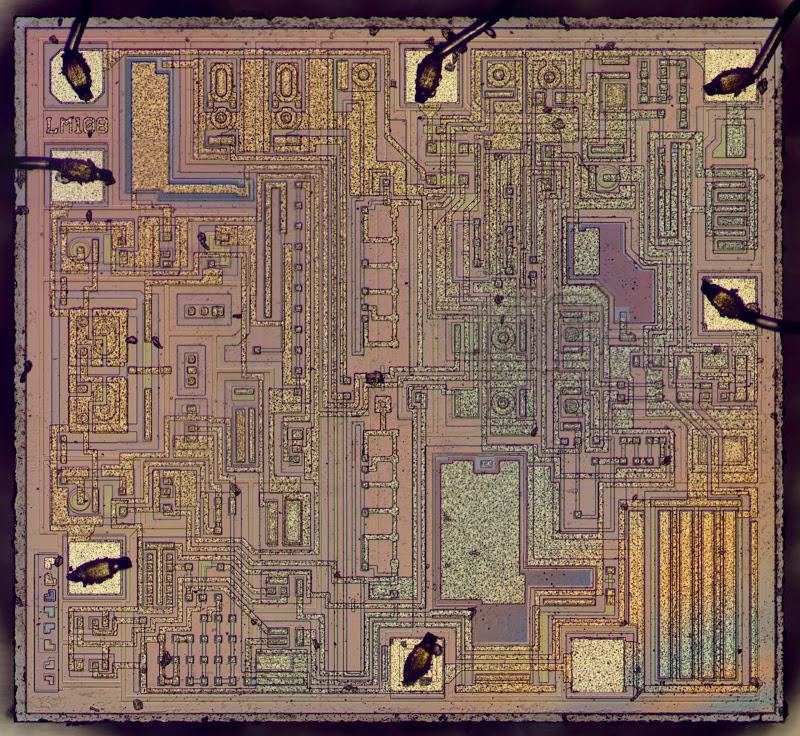
The photo above shows the LM108 op amp in a metal can. (The LM308 is the commercial-grade version of the LM108.[4] ) I opened up the can and photographed the die (below). The chip's metal layer is clearly visible, with thin metal traces connecting the different parts of the chip. The square bonding pads around the edge of the chip are connected by thin wires to the chip's external pins. Under the metal layer, you can see the silicon that forms the basis of the chip. To form transistors and resistors, a process called doping treats regions of the silicon with elements such as phosphorus or boron. In the die photo, these regions have a slightly different color, which makes the structure of the chip visible under the metal.

Die photo of the LM308 op amp. The LM308 is the commercial version of the LM108.

Die photo of the LM308 op amp. The LM308 is the commercial version of the LM108.

While the chip seems incomprehensible at first, close examination reveals the different components and their connections. By carefully studying the die photo, I reverse engineered the circuit for the op amp. Surprisingly, this chip has an unusual circuit design, more modern than National Semiconductor's "classic" LM108 design. Although the package has the National Semiconductor logo, the internal circuitry matches the Motorola LM308 datasheet.[5] You might expect that LM108's would all be the same internally, but as with many ICs, the part number doesn't indicate as much as you expect. Different manufacturers have widely differing implementations of the chip, so you can't expect two chips to behave the same just because they have the same name.[6] Even so, it's puzzling that a National Semiconductor chip doesn't match the National Semiconductor schematic.

Why op amps are important

The function of an op amp is to take two input voltages, subtract them, multiply the difference by a huge value (100,000 or more), and output the result as a voltage. If you've studied analog circuits, op amps will be familiar to you, but otherwise this may seem like a bizarre and pointless device. How often do you need to subtract two voltages? And why would you want to amplify by such a huge factor? Would amplifying a 1 volt input result in lightning shooting from the op amp?

It turns out that op amps are extremely useful and versatile, making them a key component in analog circuits. With simple feedback circuits, you can use an op amp as an amplifier, a filter, integrator, differentiator, or a variety of other circuits.[7] When an op amp is in use, the voltages on the two inputs will normally be almost identical, so multiplying by the huge amplification factor yields a reasonable output of a few volts. The point of the high amplification is it improves accuracy, even if the amplification of the overall circuit is small.

Transistors inside the IC

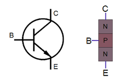
Transistors are the key components in a chip. The LM108 op amp uses NPN and PNP bipolar transistors, while many newer op amps use low-power CMOS transistors instead. If you've studied electronics, you've probably seen a diagram of an NPN transistor like the one below, showing the collector (C), base (B), and emitter (E) of the transistor. A transistor is usually illustrated as a sandwich of P silicon in between two symmetric layers of N silicon; the N-P-N layers make an NPN transistor. But it turns out that transistors on a chip look nothing like this, and the base often isn't even in the middle!

Symbol and oversimplified structure of an NPN transistor.

Symbol and oversimplified structure of an NPN transistor.

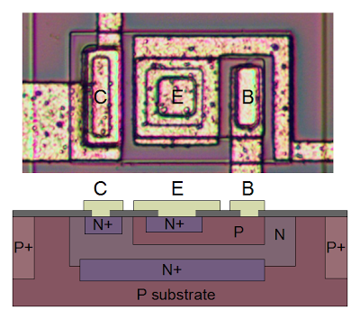
The photo below shows an NPN transistor on a 741 op amp die. The different brown and purple colors are regions of silicon that has been doped differently, forming N and P regions. The whitish-yellow areas are the metal layer of the chip on top of the silicon—these form the wires connecting to the collector, emitter, and base.

Underneath the photo is a cross-section drawing showing approximately how the transistor is constructed. There's a lot more than just the N-P-N sandwich, but if you look carefully at the vertical cross section below the 'E', you can find the N-P-N that forms the transistor. The emitter (E) wire is connected to N+ silicon. Below that is a P layer connected to the base contact (B). And below that is an N+ layer connected (indirectly) to the collector (C).

Structure of an NPN transistor in the 741 op amp

Structure of an NPN transistor in the 741 op amp

The innovative feature of the LM108 is the superbeta transistor, seen below. It has a much thinner base region below the emitter. This gives the superbeta transistor a much higher beta (i.e. amplification), but makes the transistor much more delicate: just 4 volts between the collector and emitter can "punch through" the thin base and destroy the transistor.

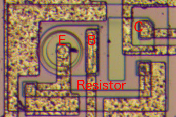
This image shows one of the superbeta transistors in the LM308 op amp. Note the large, round emitter. The green rectangle below the transistor is a resistor.

This image shows one of the superbeta transistors in the LM108 op amp. Note the large, round emitter. The green rectangle below the transistor is a resistor.

How the op amp works

In this section, I'll give a simplified overview of how the op amp works.[8] First I'll explain the differential pair, the important circuit that subtracts and amplifies the two input voltages. The next section explains the different parts of the LM108 op amp. The final section describes the current mirror that provides precise currents to the op amp's circuits.

The differential pair

The key component of an op amp is the differential pair, which is the most common two-transistor subcircuit used in analog ICs.[9] You may have wondered how the op amp subtracts two voltages since it's not obvious how to make a subtraction circuit. This is the job of the differential pair.

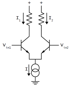
Schematic of a simple differential pair circuit. The current sink sends a fixed current I through the differential pair. If the two inputs are equal, the current is split equally between the two branches. Otherwise, the branch with the higher input voltage gets most of the current.

Schematic of a simple differential pair circuit. The current sink sends a fixed current I through the differential pair. If the two inputs are equal, the current is split equally between the two branches. Otherwise, the branch with the higher input voltage gets most of the current.

The schematic above shows a simple differential pair. The current sink at the bottom provides a fixed current I, which is split between the two input transistors. If the input voltages are equal, the current will be split equally into the two branches (I1 and I2). If one of the input voltages is a bit higher than the other, the corresponding transistor will conduct more current, so one branch gets more current and the other branch gets less. A small input difference is enough to direct most of the current into the "winning" branch, providing the amplification.

The LM108 op amp circuit

In this section, I'll give a brief explanation of the LM108 circuit, based on a detailed discussion by Bob Widlar, the chip's designer.[10] The schematic below is simplified to show the key features.

The superbeta transistors Q1 and Q2 are the heart of the chip. These form the input stage, and are connected as a differential pair. Resistors R1 and R2 provide the load for the two branches of the differential pair. By using superbeta transistors for the input, the LM108 achieves high performance with very low input currents.

The problem with superbeta transistors is they will break down and be destroyed by a small voltage difference, just 4 volts. The LM108 uses a couple interesting circuits to protect the superbeta transistors. The first protection mechanism is the two diodes across the inputs, ensuring the voltage difference is small. (On the chip, these diodes are implemented with transistors.) The second protection mechanism is transistors Q5 and Q6, which ensure that the collector-emitter voltage across the superbeta transistors is essentially zero, preventing an overload. Transistors Q3 and Q4 "bootstrap" the desired voltage from Q1/Q2's emitters to Q5 and Q6.[11]

Simplified schematic of the LM108 op amp.

Simplified schematic of the LM108 op amp from the chip's application notes.[10]

The second stage of amplification is provided by PNP transistors Q9 and Q10. They form a second differential amplifier that amplifies the output of the first stage. Instead of resistors, Q15 and Q16 form the load for the second stage differential amplifier. Transistors Q7 and Q8 bias the inputs of Q9 and Q10 to the right level.

The output of the op amp is driven by a high-current class AB amplifier with power transistors Q13 and Q14. That is, Q13 will pull the output high and Q14 will pull the output low. To ensure that the right output transistor turns on at the right time, Q11 and Q12 bias the output transistors (by two diode drops).

IC component: The current mirror

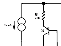
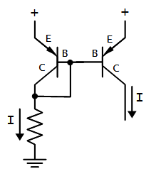
The schematic above uses a symbol that you may not be familiar with: the double circles that indicate a current source. A current source may seem like a strange concept, but it is very common in analog integrated circuits. The idea is that instead of controlling currents with resistors (which are inconveniently large and inaccurate on ICs), currents are generated from a current mirror.[12] Once you have one fixed current, you can use a current mirror to generate copies of this current. Simple modifications can scale the current or even invert it.

Detail of the LM108 op amp schematic, showing the current source symbol.

Detail of the LM108 op amp schematic, showing the current source symbol.

The diagram below shows how a current mirror is implemented.[12] A reference current passes through the transistor on the left. (In this case, the current is set by the resistor.) Since both transistors have the same emitter voltage and base voltage, they source the same current, so the current on the right matches the reference current on the left. Thus, the current mirror provides a mirror image on the right of the fixed current on the left.

Current mirror circuit. The current on the right copies the current on the left.

Current mirror circuit. The current on the right copies the current on the left.

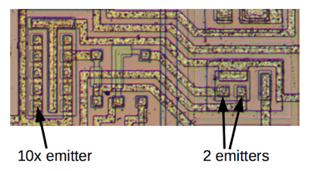
In the LM108, the initial current is generated not by a resistor, but by a patented four-transistor circuit that depends on one transistor having 10 times the emitter area of the others. The photo below shows the transistor that combines 10 square emitters into one large emitter, as well as an unusual transmitter with two separate emitters.[13]

The LM308's current source contains some interesting transistors. The transistor on the left has 10 emitters wired together, creating a transistor with an effective emitter size of 10 times normal. The transistor on the right has two separate emitters, providing two current outputs.

The LM108's current source contains some interesting transistors. The transistor on the left has 10 emitters wired together, creating a transistor with an effective emitter size of 10 times normal. The transistor on the right has two separate emitters, providing two current outputs.

Interactive chip viewer

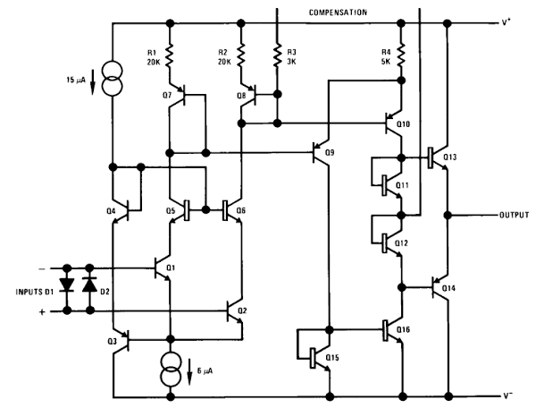
The image and schematic[5] below are an interactive exploration of the LM108. Click a component to see its location on the die and in the schematic highlighted. The box below will give an explanation of the component. The schematic below is the full schematic for the LM108; the component numbers don't match the earlier simplified schematic.

Click components in the image below for more information.

How I photographed the op amp die

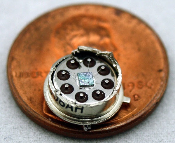
Usually getting the die out of an IC requires concentrated acid to dissolve the epoxy package. But some ICs, such as op amps, are available in metal cans (for shielding) which can be easily opened with a hacksaw (or even better a jeweler's saw). I used a metallurgical microscope for my die photos, but you can use even a basic middle-school microscope to see many of the chip features. The photo below shows the LM108 op amp after removing the top. The tiny die is visible in the center, with thin wires connecting the die to the pins that surround it. The metal tab on the right indicates pin 8. To create the high-resolution die photo, I composited multiple photographs into one image (details).

The LM308 op amp has been cut open revealing the tiny die inside. Pads on the die are connected to the pins with thin bond wires.

The LM308 op amp has been cut open revealing the tiny die inside. Pads on the die are connected to the pins with thin bond wires.

Some strange things in the LM108 die

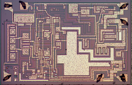
The LM108 die is more complex than I expected and has some strange circuitry. If you compare the 741 op amp (below) with the LM108, you'll notice that the 741 is much simpler. Part of this is the LM108 has 30 transistor versus 22 in the 741, but this small increase in components doesn't explain the large increase in the intricacy of the LM108. After examining the LM108 closely, I realized that it has many components on the die that aren't used. More investigation revealed that the LM108 die can be reused to create an entirely different op amp, the LM11![14] The manufacturer can use the same die (with a few changes to the metal wiring layer) to produce two different integrated circuits, which presumably saves them money.

Die photo of the 741 op amp

Die photo of the 741 op amp. This chip is much simpler than the LM108.

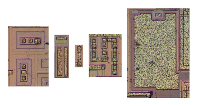
The photo below shows some of the unused components on the LM108 die. On the left are two unused transistors, including one with two emitters. Next is a larger transistor. The small component is a resistor that is shorted out by the metal on top of it, making it nonfunctional. Seven diodes are connected in an undulating chain, but the chain isn't connected to anything. Finally, the chip has two large unused capacitors, one of which is shown below. I was puzzled by the amount of space wasted on the die for these unused components.

The LM308 integrated circuit contains an unusual number of unused components. This image shows some of them: two transistors , a larger transistor, a resistor that is shorted out, a chain of diodes, and a capacitor.

The LM108 integrated circuit contains an unusual number of unused components. This image shows some of them: two transistors, a larger transistor, a resistor that is shorted out, a chain of diodes, and a capacitor.

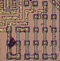
Another puzzle on the LM108 die is it has several resistors that are made up of multiple segments. By shorting out some of these segments with the metal layer, the resistance can be tuned to a desired value.[15] The mystery is why the LM108 die has so many resistances that need to be customized.

The LM308 op amp contains several resistors with resistance than can be modified by changing the metal layer. This image shows one resistor with about 20 segments. A few of the segments are shorted out with metal, reducing the resistance.

The LM108 op amp contains several resistors with resistance than can be modified by changing the metal layer. This image shows one resistor with about 20 segments. A few of the segments are shorted out with metal, reducing the resistance.

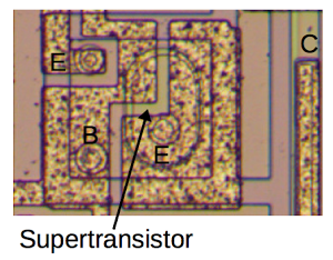
Another strange feature of the LM108 die is the protection transistors are unusually large and have extra unused structures (below). The transistor has two emitters: one is a regular emitter, and the second is a large, oval superbeta transistor emitter. The superbeta emitter is not wired to anything, which raises the question of why it exists. The die has other strange, unused transistors.[16]

This unusual transistor from the LM108 has two emitters: one has a regular base and one has a supertransistor base. The second emitter is not connected to anything.

This unusual transistor from the LM108 has two emitters: one has a regular base and one has a supertransistor base. The second emitter is not connected to anything.

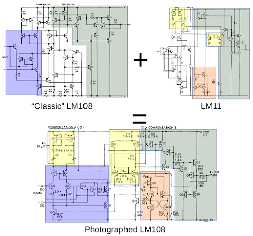
By studying the schematics closely, I think I solved the puzzle of these strange and unused components. I determined that the LM108 I examined is a combination of the "classic" LM108 and the LM11 op amp introduced in 1980. The diagram below shows that my chip uses the input stage from the classic LM108 (blue). But the second stage (yellow) and the current source (red) matches the LM11. All chips use the same output stage (green).

The LM108 I examined (bottom) is a combination of the 'classic' LM108 and the more modern LM11 op amp. It takes the input stage from the classic (blue) and the second stage (yellow) and the current source (orange) from the LM11. All three op amps use the same output stage (green).

The LM108 I examined (bottom) is a combination of the 'classic' LM108 and the more modern LM11 op amp. It takes the input stage from the classic (blue) and the second stage (yellow) and the current source (orange) from the LM11. All three op amps use the same output stage (green).

My conclusion is the die is designed so it can be used both as an LM11 and an LM108, by just making some changes to the metal layer. Thus, when configured as an LM11, the chip uses the components that are unused in the LM108. The LM11 schematic shows a zener diode for protection: this is the unused chain of diodes shown earlier. The LM11 makes use of the other unused resistors, transistors, and capacitors described above. Finally, the two protection transistors in my LM108 look like a combination of a regular transistor and an unused superbeta transistor. The LM11 schematic shows weird transistors that are half regular and half superbeta, an exact match for these puzzling transistors.

Conclusion

Every IC die has its own interesting puzzles and features, and the LM108 is no exception. The LM108 is an interesting chip since it uses superbeta transistors for high performance, but requires internal protective circuitry to keep the delicate transistors safe from damage. The most unusual thing about this LM108 is that the same chip die is used for both the LM108 and the LM11 op amps, just by tweaking the metal layer. While this makes the die more complex, presumably it saves money for the manufacturer.

Thanks to Bil Herd (famed designer of the Commodore 128) for suggesting the LM108 as an interesting chip to examine. /r/AskElectronics had an informative discussion of the LM108's strange transistors; thanks to crb3 for pointers to relevant documents.

I announce my latest blog posts on Twitter, so follow me at kenshirriff.

Notes and references

[1] By all reports, Robert Widlar was an amazing analog engineer, as well as an alcoholic crazy guy. Widlar invented key analog IC circuits such as the Widlar current source as well as groundbreaking ICs such as the µA702 and µA723. In 1970 he sold his stock options for a million dollars (about 6 million adjusted for inflation) and retired to Mexico at 33. Some entertaining stories about him are here, on Wikipedia, and with pictures of his sheep.

[2] The 741 has up to 1.5µA input bias current, while the LM108's maximum input bias current is orders of magnitude lower at 3nA.

[3] The base of a regular transistor is 0.5 to 1µm thick, while a superbeta transistor has a much thinner base of 0.1 to 0.2µm. According to an Application Note on the LM108, the superbeta transistor has a gain of 5000, compared to 200 for a regular NPN transistor. The downside is the superbeta transistors have a breakdown voltage of 4 volts, compared to 80 for regular transistors.

[4] The first digit of the part number specifies the temperature range. The LM108 is the military-grade chip that can handle the widest temperature range, the LM208 is the industrial-grade chip, and the LM308 is the commercial-grade chip with the narrowest temperature range. The "H" in LM308AH indicates the metal can package.

[5] The LM108 schematic that matches my die photo is from the Motorola LM108 datasheet. It is strange that my chip is labeled National Semiconductor but its circuit does not match the National Semiconductor datasheet. Instead it matches the Motorola datasheet.

Another variant of the LM108 is the Raytheon design (datasheet). This version has a totally different second stage, output stage, and current biasing. It uses many more transistors: 48 transistors including 6 superbeta devices.

[6] The LM108 is used in distortion pedals; people search out this op amp to get its specific sound quality when overdriven. Since different manufacturers have different internal designs for the LM108, this raises the question of whether people may unexpectedly end up with different op amps that produce different sound effects.

[7] To see the variety of circuits that can be built from an op amp, see this op amp circuit collection. The book Op Amp Applications Handbook has a ton of useful information about op amp types (including the LM108), applications, and history; it is also available as a PDF.

[8] IC Op-Amps Through the Ages. Op Amp History (Walt Jung) page H.52 (also here) discusses the LM108 in more detail.

[9] Differential pairs are also called long-tailed pairs. According to Analysis and Design of Analog Integrated Circuits differential pairs are "perhaps the most widely used two-transistor subcircuits in monolithic analog circuits." (p214) For more information about differential pairs, see wikipedia, any analog IC book, or chapter 4 of Designing Analog Chips. The latter is an excellent book written by Hans Camenzind, the inventor of the 555 timer, so definitely check out the PDF version.

[10] Widlar wrote a detailed explanation of the LM108 in IC Op Amp Beats FETs on Input Current (National Semiconductor Application Note 29, Dec 1969).

[11] To protect the input transistors, transistors Q3 and Q4 boost the input transistor emitter voltage by two diode drops to make the voltages match. Transistors Q5 and Q6 are in a cascode configuration. The result is the collector-base voltage of the input transistors is effectively zero, protecting them.

[12] A current mirror is a very useful way of connecting transistors so the current through the second transistor matches the current through the first transistor. For more information about current mirrors, you can check Wikipedia or any analog IC book such as chapter 3 of Designing Analog Chips.

[13] The LM108's four-transistor current source is configured so the four base-emitter junctions cancel out, except that one transistor has 10 times the base area of the remainder. The voltage generated across R20 is kT/q * ln(10), which is approximately 60mV at room temperature, but proportional to absolute temperature. (The principle of using emitters of different areas is similar to a bandgap voltage reference. However, the bandgap reference is configured so the temperature dependency cancels out and the voltage is stable.) The resistance of R20 controls the current into the current mirror. The temperature dependence is used to counteract temperature dependence of other parts of the circuit.

A field-effect transistor (Q30) generates the small current that powers the LM108's current source. The current source circuit turns the unpredictable current from Q30 into a stable output current. For a full explanation, see patent 3930172.

[14] The LM11 op amp is discussed in detail in Reducing DC Errors in Op Amps (National Semiconductor Technical Paper 15) by Widlar.

[15] In some precision chips, the resistance can be tuned on a per-chip basis, for instance by laser-trimming the resistor or using Zener zapping. This is not the case in the LM108; the resistances are controlled by the metal layer, which requires a new mask if it is changed.

[16] Two more strange transistors are shown below, with unconnected oval emitters.

Closeup of two strange transistors on the LM308 die.

Closeup of two strange transistors on the LM108 die.

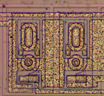
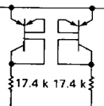
The schematic symbol (below) is even more puzzling, showing transistors with two emitters and two bases. While transistors with two emitters are common in integrated circuits, I've never seen two bases in one transistor. After discussion on /r/AskElectronics, my theory is the second emitter is tied off on the LM108 but used on the LM11 for the balance inputs.

Symbol on the schematic for two strange transistors inside the LM108 op amp.

Symbol on the schematic for two strange transistors inside the LM108 op amp.