Tenma 72-7740 multimeter: review and teardown

The Tenma 72-7740 digital multimeter is a multimeter in the $70 price range. Overall, it's a nice, solidly-build meter and it has performed well for me. I received this DMM from Newark element14 for review; in this article I describe its functionality followed by a teardown.

What you get

What comes in the box with the Tenma 72-7740 DMM: temperature probe, battery, alligator clips, and probes.

The DMM comes with a temperature probe, battery, alligator clips, and test probes. Note that the test probes have very short metal tips, unlike the long tips on most probes. The alligator clip probes are a nice addition. My biggest complaint with the DMM is the temperature probes connections are soldered with no strain relief so I worry the wires will break off.

The DMM also comes with a pocket-sized 36 page operating manual - a real, physical manual on paper, not a PDF file like most products these days. The DMM doesn't really need a manual - functions work pretty much as you'd expect - but it's nice to have the manual.

Specifications

The DMM is autoranging with maximum reading of 3999. It is full-size (177mm × 85mm × 40mm), not a pocket DMM, and has a built-in stand. The LCD display is large and clear and has a backlight, which is nice if I ever end up using the meter in the dark. It has 10MΩ input impedance and maximum voltages of 1000V DC and 750V AC. The top current range is 10A.

The DMM also includes capacitance, diode, temperature, frequency, and duty cycle measurements. The top capacitance range (100µF) can take up to 15 seconds to get a measurement, so be patient with those big electrolytics. The lowest capacitance range is 40 nF with 10pF resolution claimed. The DMM also has a continuity buzzer, although I find the sound crackles a bit. The temperature readings are only in °C; I know using Fahrenheit makes me a bad person, but that's what I need to check my appliances. The temperature range is -40°C to 1000°C. The upper range is hotter than I need, but since I sometimes go outside below -40°C my multimeter should be able to handle it too.

Buttons provide hold and relative mode. The meter goes into sleep mode after 30 minutes.

I don't have the equipment to measure the accuracy of the DMM myself, so I'm going off the published values. The specification for DC voltage accuracy is a reasonable ±0.8%; the considerably more expensive Fluke 177 has ±0.09% accuracy, so you get what you pay for.

The function knob has 7 positions: V, resistance/capacitance/diode/continuity, Hertz, °C, µA, mA, and A. The blue function button switches between AC and DC or switches among resistance, capacitance, diode, and continuity.

There are a few functions found in more advanced multimeters that aren't found here: min/max measurement, RS-232 support, °F, a 4nF capacitance scale, and an analog bar graph.

For full specifications, see the specification chart.

Tenma 72-7740 digital multimeter measuring 60Hz line frequency

Tenma 72-7740 digital multimeter measuring 60Hz line frequency

Teardown

Of course I was interested in what was inside the multimeter and opened it up. The instruction manual describes how to remove the screws under the feet. The force required to pry the case apart made me a little nervous, but it snapped open without breaking anything. Note that the case must also be opened in this way to replace the fuses - they are not accessible from the battery compartment. Unfortunately I tend to blow fuses a lot measuring charger performance, but this may motivate me to be more careful.

Inside the Tenma 72-7740 DMM, showing the foil shield, the two fuses, and the thick wire for high-current measurements.

A foil shield covers most of the circuit board, with holes for some adjustments. Near the bottom is a thick wavy wire, which is the precision resistor used for the high-current measurements, a fraction of an ohm. There's nothing particularly interesting directly under the foil shield; almost all the components are on the other side.

Removing the circuit board and flipping it over shows the circuitry. The large LCD display is at the top, with the pushbuttons below. The most visually striking part of the board is the round circuitry for the function knob, which I will explain in more detail below. To the left are three precision (blue) resistors for mA and µA measurement. Below are 5 diodes which I believe are for input protection. The large black cylinder in the lower right appears to be a spark gap to protect the input from high voltages - the DMM is rated to 1000V DC overload protection. Below it is a large yellow PTC resistor to protect from input overloads. The 8-pin IC is a STMicroelectronics TL062C low power J-FET dual op amp.

The circuit board for the Tenma 72-7740 DMM.

The circuit board for the Tenma 72-7740 DMM.
Underneath the LCD is the 100-pin controller IC and a bunch of SMD components. The Semico CS7721CN chip powers the Tenma 72-7740 DMM. I wasn't expecting that a DMM chip would need 100 pins, but that seems to be common. I couldn't find a datasheet for this specific chip, but datasheets for other similar chips (such as the Fortune FS9721 and Cyrustek ES51982) give an idea of how digital multimeters works. The chip has signal inputs for the different functions (voltage, current, resistance, frequency, capacitance, etc.) The four blue precision resistors below the chip divide the input by powers of 10 as appropriate. Six mode pins are connected to the function selector switch to select the appropriate function, as will be displayed below. The function pushbuttons are also connected to the IC. About 17 pins from the IC drive the LCD segments. The crystal provides accurate timing, which is critical for the accuracy of the dual-slope analog-to-digital converter that measures the input.

The 100-pin Semico CS7721CN chip powers the Tenma 72-7740 DMM.

The 100-pin Semico CS7721CN chip powers the Tenma 72-7740 DMM.

How the function selector switch works

Rotary switches have always been mysterious to me. The pattern on the circuit board seems to be made up of random lines rather than any obvious switch contacts, and looks as much like an Aztec symbol as a switch. So I figured it was time to dive in and figure out how it works.

The selector knob has 7 positions, rotating a bit under 180 degrees in total. Looking at the back of the selector knob, you can see six independent sliders for six separate switching circuits. Each slider has two peaks in the middle, which bridge two contacts on the circuit board. Note that the two outermost sliders are offset 90 degrees from the others. Since the knob turns a bit under 180°, the sliders n

The function knob rotates through seven positions and has six independent contacts.

The following diagram shows how the switches work. Each of the six colored semi-circular rings is associated with one of the sliders. The seven lines inside each semicircle indicate the seven possible positions of the associated slider. The most counterclockwise position in each ring is the V setting, followed by Ω, Hz, °C, µA, mA, and A. If there are two traces lined up with the slider, the slider will connect the two traces.

This diagram shows the structure of the function switch on the Tenma 72-7740. Each color shows one of the six independent switches, with lines for the seven possible positions. In highlighted positions, a pair of contacts is closed.

One surprise is that many of the traces don't actually form a circuit. The highlighted positions in the diagram are active positions that close two contacts, but the other positions don't form a connection. In particular, the red ring is only active in one position, and the blue ring in two positions. Many positions have the same circuit trace on both ends of the line, which means the switch does nothing and the trace is unnecessary. My guess is that the redundant metal is there because metal-on-metal is lower friction than metal-on-circuit-board.

The white, cyan, and blue rings ground various combinations of "mode" pins on the IC to select the function. The left half of the purple ring directs the µAmA°C input to the appropriate circuit based on the function. The right half of the purple ring directs the HzVΩ input appropriately. The red ring has a connection only for the °C setting. The orange ring makes connections for Ω, °C, and A.

Conclusion

The 72-7740 DMM is a solid meter that gets the job done and I have only minor complaints. It currently sells for about $70. Inexplicably, the next model up, the 7745, is cheaper despite having true RMS and a serial RS-232 output. The model down, the 7735 is a good deal at about half the price; it also has RS-232, although it lacks temperature measurement, the backlight, and sleep mode.

The Tenma 72-7740 DMM in the box.

The Tenma 72-7740 DMM in the box.

Thanks to Newark element14 for giving me this digital multimeter free for review. (Newark element14 consists of the merger of the well-known Newark electronics distributor and the element14 online electronics community into a single global brand.)

Wealth distribution in the United States

Today's Forbes billionaires list inspired me to visualize the wealth inequality in the United States. Use the Forbes list and other sources, I've created a graph that shows wealth distribution in the United States. It turns out that if you put Bill Gates on a linear graph of wealth, pretty much the entire US population is crammed into a one-pixel bar around 0.

This graph shows the wealth distribution in red. Note that the visible red line is one pixel wide and disappears everywhere else - this is the key point: essentially the entire US population is in that first bar. The graph is drawn with the scale of 1 pixel = $100 million in the X axis, and 1 pixel = 1 million people in the Y axis. Away from the origin, the red line is invisible - less than 1/1000 of a pixel tall since so few people have more than $100 million dollars. It's striking just how much money Bill Gates has; even $100 million is negligible in comparison.

Since the median US household wealth is about $100,000, half the population is crammed into a microscopic red line 1/1000 of a pixel wide. (The line would be narrower than the wavelength of light so it would be literally invisible). And it turns out the 1-pixel-wide red line isn't just the "99%", but the 99.999%. I hypothesize this is why even many millionaires don't feel rich.

Wealth inequality among billionaires

Much has been written about inequality in the US between the rich and the poor, but it turns out there is also huge inequality among the ranks of billionaires. Looking at the 1.9 trillion dollars held by US billionaires, it turns out that the top 20% of billionaires have 59% of this wealth, while the bottom 20% of billionaires have less than 6%. So even among billionaires, most of the money is skewed to the top. (I originally pointed this out in Forbes in 1998, and the billionaire inequality has grown slightly since then.)

Sources

The billionaire data is from Forbes billionaires list 2013. Median wealth is from Wikipedia. Also Measuring the Top 1% by Wealth, Not Income and More millionaires despite tough times. Wealth data has a lot of sources of error including people vs households, what gets counted, and changing time periods, but I've tried to make this graph as accurate as possible. I should also mention that wealth and income are two very different things; this post looks strictly at wealth.

The 8085's register file reverse engineered

On the surface, a microprocessor's registers seem like simple storage, but not in the 8085 microprocessor. Reverse-engineering the 8085 reveals many interesting tricks that make the registers fast and compact. The picture below shows that the registers and associated control circuitry occupy a large fraction of the chip, so efficiency is important. Each bit is implemented with a surprisingly compact circuit. The instruction set is designed to make register accesses efficient. An indirection trick allows quick register exchanges. Many register operations use the unexpected but efficient data path of going through the ALU.

While the 8085's register complement is tiny compared to current processors, it has a solid register set by 1977 standards - about twice as many registers as the 6502. The 8085 has a 16-bit program counter, a 16-bit stack pointer, 16-bit BC, DE, and HL register pairs, and the 8-bit accumulator. The 8085 also has little-known hidden registers that are invisible to the programmer but used internally: the WZ register pair, and two 8-bit registers for the ALU: ACT and TMP.

Photograph of the 8085 chip showing components relevant to register operations.

Photograph of the 8085 chip showing components relevant to register operations.

The register file is in the lower left quadrant of the chip. It contains the 6 register pairs and associated circuitry. Underneath the registers is the 16-bit address latch and increment/decrement circuit. The register file is controlled by a set of control lines on the right, which are driven by register control logic circuits and the register control PLA. The current instruction is loaded into the instruction register (upper right) via the data bus. In the upper left is the 8-bit arithmetic-logic unit (ALU), with the accumulator and two temporary registers (ACT and TMP).

The 8085 has only 40 pins (visible around the edge of the image) to communicate with the outside world, a tiny number compared to current microprocessors with more than 1000 pins. For memory accesses, the 8085 reads or writes 8 bits of data using a 16-bit memory address (for a maximum of 64K of memory). In the image above, memory addresses flow through the 16-bit address bus (abus) provides memory addresses, while data flows through the chip over the 8-bit data bus (dbus). The 8 A pins handle half of the address, while the 8 AD pins are used both for the other half of the address and for data (at different times). This frees up pins for other uses, but makes computers using the 8085 slightly more complicated. In comparison, the 6502 is more straightforward, with separate pins for address and data.

Overall architecture of the register file

The diagram below shows the implementation of the 8085 register file in the same layout as on the actual chip. The 8-bit data bus is at the top, and the 16-bit address bus is at the bottom. The register control lines are on the right.

In the middle are the registers, arranged as pairs of 8-bit registers. Note that the registers are arranged "backwards" with the high-order bit on the right and the low-order bit on the left. The 16-bit program counter and stack pointer are first. Next is the WZ temporary register, and underneath it the BC register pair. The HL and DE register pairs are at the bottom - these registers do not have fixed locations, but can swap roles during execution. A 16-bit register bus (regbus) provides access to the registers.

Underneath the registers is the address latch, which holds a 16-bit value that is written to the address bus. This value is also the input to the 16-bit increment/decrement circuit. The output of the incrementer/decrementer can be written back to the registers.

The triangles indicate tri-state buffers, basically switches that control the flow of data. Buffers containing a + are amplifiers to boost the weak signals from the registers. Buffers containing a S are superbuffers, that provide extra current to send data across the long data bus.

Architecture diagram of the 8085 register file, as it is implemented on the chip. The register file is connected to the data bus at top, and address bus at bottom. The control lines are along the right.

Architecture diagram of the 8085 register file, as it is implemented on the chip. The register file is connected to the data bus at top, and address bus at bottom. The control lines are along the right.

The picture below zooms in on the chip image above, showing the register file in detail. The components in silicon exactly map onto the diagram above. Note the repeated patterns for the 16-bit circuits. The large transistors used as high-current drivers are clearly visible. The transistors in each bit of register storage are much smaller.

A closeup of the 8085 microprocessor, showing the details of the register file and the locations of the major components.

A closeup of the 8085 microprocessor, showing the details of the register file and the locations of the major components.

Storing bits in the register file

The implementation of the 8085 registers is unusual in several ways. The registers don't have explicit read and write modes; instead the register will be overwritten if there is a stronger signal on the bus. Instead of having a bus with one wire for each bit, the 8085 uses a sort of differential bus, with two wires for each bit: one wire transmits the value, and the other transmits the complement of the value.

Each bit consists of two inverters in a feedback loop, with pass transistors to connect the inverters to the bus. An unusual feature of this is the lack of any circuit to break the feedback loop when modifying the register (unlike the 6502). Instead, the 8085 uses a "might makes right" technique - if a stronger signal is written to the bus, it will overwrite a register connected to the bus. The transistors driving the register bus are about twice as large as the transistors in the inverters, so they can forcibly overwrite the inverter loop.

One consequence of this register implementation is that a register can't be copied directly to another register, since there's nothing to distinguish the source register from the destination register - each register could potentially damage the other's bits. To get around this, the 8085 uses an interesting trick - copies are actually done through the ALU, as will be explained later.

One bit of a register in the 8085 register file. Each bit is stored in two inverters in a feedback loop. The register bus uses two lines of opposite polarity for each bit. Access to the register is controlled by the reg_rw control line, which connects the inverters to the bus, allowing the value to be read or written.

One bit of a register in the 8085 register file. Each bit is stored in two inverters in a feedback loop. The register bus uses two lines of opposite polarity for each bit. Access to the register is controlled by the reg_rw control line, which connects the inverters to the bus, allowing the value to be read or written.
The image below zooms in on the chip closer, showing the silicon for six individual register bits. The schematic for one bit is overlaid, as are some of the metal lines providing power, ground, and the register bus. Each bit consists of two transistors for the inverters, two depletion pullup transistors for the inverters (shown as resistors), and two pass transistors connecting the bit to the register bus. The pink regions are transistors, with the green strips the gates (details).

Detail of the 8085 chip showing six bits in the 8085's register file. Bit 2 of the stack pointer is shown with schematic. The two transistors form two inverters in a feedback loop. The light blue lines are the metal layer wires connected to bit 2. The program counter is in the upper half of the image.

Detail of the 8085 chip showing six bits in the 8085's register file. Bit 2 of the stack pointer is shown with schematic. The two transistors form two inverters in a feedback loop. The light blue lines are the metal layer wires connected to bit 2. The program counter is in the upper half of the image.

To read a register, an amplifier circuit is used to boost the signal from the differential register bus to write it to the dbus or address latch. I assume this is a tradeoff to make the register file smaller. Each inverter pair can be made as small as possible, but then requires amplification to produce a signal strong enough for use elsewhere in the chip. The amplification circuit that drives the data bus is more complex than I'd expect, probably because of the extra power to drive the bus (details and schematic).

The incrementer/decrementer

The 16-bit incrementer/decrementer at the bottom of the register file is used for multiple purposes. It increments the program counter as instructions execute, increments and decrements the stack pointer as needed, and supports the 16-bit increment and decrement instructions.

An interesting feature of the incrementer is it also supports incrementing by 2, which is used to quickly skip over the two byte address in a call or jump not taken. This allows these operations to complete faster on the 8085 than the 8080.

Two bits of the 16-bit increment/decrement circuit in the 8085. Odd bits and even bits use a different circuit for efficiency. The carry out from even bits is complemented.

Two bits of the 16-bit increment/decrement circuit in the 8085. Odd bits and even bits use a different circuit for efficiency. The carry out from even bits is complemented.

The incrementer/decrementer is implemented by a chain of adders with ripple carry - the carry from each bit flows into the adder for the next bit. (The above schematic shows two bits, and is repeated 8 times in the full circuit.) The DREG_INC and DREG_DEC control lines select increment or decrement. One performance trick is that alternating bits are implemented with different circuits and the carry out of even bits is inverted. This avoids the inverters that would otherwise be needed to flip the carry back to its regular state. This saves space, but even more importantly it speeds up carry propagation. Because the carry has to propagate bit-by-bit through all 16 bits to generate the final result, adding an inverter to each bit would slow it down significantly. The carry out is used to compute the undocumented K flag value (details).

In comparison, the 6502 has a 16-bit incrementer (no decrement) used exclusively by the program counter. To reduce the carry propagation speed, this incrementer uses a carry-skip. That is, the carry out of the low-order byte is immediately generated and fed into the high-order byte. Thus the carries only need to propagate through 8-bits, the two bytes working in parallel. (The carry is easily generated by ANDing together the low-order bits. If they are all 1, there will be a carry into the high-order byte.)

The WZ Temporary registers

The WZ register pair in the 8085 is used for temporary storage, but is invisible to the programmer. Internally, the WZ register pair is implemented like the other register pairs.

The primary use of WZ is to hold operands from a two or three byte instruction until it can be used. The WZ registers are used to hold 16-bit addresses for LDA, STA, LHLD, JMP, CALL, and RST instructions. The registers hold the port for IN and OUT. The WZ register pair can also temporarily hold information read from memory. The registers hold the address popped off the stack for RET. For XTHL, the registers hold the value from the stack.

Register decoding and the instruction set

The instruction set of the 8085 is organized so an instruction can be quickly and easily decoded to determine the instruction to use. The underlying structure for most 8085 instructions is the octal bit pattern bbDDDSSS, where destination bits DDD and/or source bits SSS select the register usage. The move (MOV) instructions follow this structure. Other instructions (e.g. INR) use just the DDD bits to select the register, while math instructions use the three SSS bits. Some instructions only use DDD or SSS, and some instructions operate on register pairs so they don't use the lowest bit. This instruction pattern is visible if the instructions are arranged in an instruction table according to their octal values.

The three bits select the register as follows:

D2D1D0Register
000B
001C
010D
011E
100H
101L
110M
111A

M indicates a memory operation and is treated as a pseudo-register in the instruction set. Some instructions (e.g. INX) use the top two bits to select a register pair: BC, DE, HL, or "special" (stack pointer or accumulator). Note that in the table above the low-order bit selects a register out of a register pair.

This instruction set structure allows simple logic to control the registers. A multiplexer pulls out the right group of three bits, depending on the instruction and the cycle in the instruction (link to schematic). These three bits are then used to pick the specific register control lines to activate at each step.

The registers are controlled by about 18 control lines that affect the movement of data and the operation of the incremented/decrementer. The following table summarizes the control lines.

/RREG_RDReads the right-hand side register bus onto the data bus.
This implements the multiplexing of 16-bit registers onto the 8-bit data bus.
/LREG_RDReads the left-hand side register bus onto the data bus.
LREG_WRWrites the data bus to the left-hand side register bus.
This implements the demultiplexing of the 8-bit data bus to the 16-bit registers.
RREG_WRWrites the data bus to the right-hand side register bus.
REG_PC_RWConnects the PC to the register bus.
REG_SP_RWConnects the SP to the register bus.
REG_WZ_RWConnects the WZ register pair to the register bus.
REG_BC_RWConnects the BC register pair to the register bus.
REG_HL_RWConnects the HL (DE) register pair to the register bus.
REG_DE_RWConnects the DE (HL) register pair to the register bus.
DREG_WRWrites the output of the incrementer/decrementer to the register bus.
DREG_RDReads the register bus into the address latch.
/DREG_RDInverted DREG_RD.
DREG_DECIncrementer/decrementer performs decrement.
DREG_INCIncrementer/decrementer performs increment.
CARRY_OUTThe carry/borrow out from the incrementer/decrementer.
DREG_CNTIncrement/decrement by 1.
DREG_CNT2Increment/decrement by 2.

The first step in register control is the register control PLA, which generates 19 control signals based on the instruction type and the cycle step. The register control logic (between the register file and the PLA) mixes in the register selection bits as appropriate (and a few other inputs) to generate the register control lines listed above.

For instance, REG_BC_RW control line is activated if the PLA indicates a register access and the register bits are 00x. The RREG_RD control line is activated for a single-register read instruction if the register bits are xx0, and LREG_RD is activated if the bits are xx1. Both control lines are activated at the same time if the PLA indicates a register pair read.

The DE/HL exchange trick

The XCHG instruction exchanges the contents of the HL register pair with the contents of the DE register pair in a single M-cycle. You might wonder how the registers can be exchanged so quickly. It turns out that this instruction is implemented with a trick - an extra level of indirection.

Although most 8085 architecture diagrams label one register pair as DE and another as HL, this isn't exactly true. In fact, the 8085 has two register pairs and either one can be the DE or HL pair. A status flip flop keeps track of which pair is DE and which is HL. As Pavel Zima figured out, the XCHG instruction doesn't move any data; it simply toggles the flip flop. The data remains in the same place, but the DE register is now HL and vice versa. Thus, the XCHG instruction is completed quickly. The consequence is every use of DE or HL uses this flip flop to determine which register to access (link to schematic).

Using the ALU to move registers

You wouldn't expect the ALU (arithmetic-logic unit) to take part in a register-to-register move, but it happens in the 8085. Many register operations take advantage of the ALU's temporary registers.

The ALU doesn't directly operate on the accumulator and input register. Instead, the accumulator is copied to the ACT (Accumulator Temporary) register and the other input is copied to the TMP register. This way, the result can be written to the accumulator without the race condition that would occur if the accumulator were an input and output at the same time.

For register moves, the source value is copied to the TMP register, the ACT register is set to 0, and the ALU performs an OR operation (ALU details), writing the result (i.e. the source value) to the dbus. This result can then be stored to the register file during a later cycle.

The register file in action

The step-by-step operation of the register file is surprisingly complex. One complication is that the register file and buses must handle stepping the program counter, fetching the instruction, and performing any register moves, without interference. A second complication is that register moves go through the ALU as described above.

Stepping through an operation in detail will show the complexity of the register operations. The following shows the data flow for a MOV B,E instruction, which copies the contents of the E register into the B register.

To understand this table, a bit of background on 8085 instruction timing. An instruction cycle is broken down into one or more M (machine) cycles, where an 8-bit memory access can be done in one M cycle. Each M cycle is broken down into several T-states, where each T-state corresponds to one clock cycle. Each clock cycle has a low phase and a high phase.

The single-byte register-to-register MOV instruction takes one M cycle (M1), 4 T cycles, or 8 clock phases. Each clock phase is a separate line in the table. To make things more complicated, the activity for an instruction isn't entirely within its own instruction cycle. To improve performance, the 8085 uses simple pipelining, where the M1 opcode fetch of the next instruction overlaps with completion of the previous instruction.

The MOV B, E instruction (which copies the E register to the B register) is illustrated in the table below. The PC is copied to the incrementer latch at the end of the previous operation, and then is written to the address pins during the T1 cycle. The PC is updated with the incremented value at the end of the T2 cycle.

The instruction opcode is fetched in the T3 cycle, and at this point execution can start on the instruction. It's not until the T1 cycle of the next instruction that the register file swings into action. The E register is written to the dbus at the end of the T1 cycle. Then the ALU's TMP register is loaded from the dbus. The ALU's other argument, the ACT register is 0 at this point, and the ALU is configured to perform an OR operation. At the end of the (next instruction's) T3 cycle, the result of the ALU operation (i.e. the E register) is stored in the B register via the dbus. Meanwhile, the next instruction is getting fetched (grayed out).

CycleT/clockPC actionRegister action
T4/0
T4/1PC → inc latch
M1
opcode fetch
T1/0inc latch → address pins
T1/1inc latch → address pins
T2/0
T2/1inc → PC
T3/0data pins → dbus → instruction reg
T3/1
T4/0
T4/1PC → inc latch
M1
opcode fetch
T1/0inc latch → address pins
T1/1inc latch → address pinsE reg → dbus
T2/0dbus → TMP reg
T2/1inc → PC
T3/0data pins → dbus → instruction reg
T3/1ALU → dbus → B reg

Each step in the table above is activated by the appropriate register control lines. For instance, in T2/1, the PC is updated by triggering the reg_pc_rw and dreg_wr lines.

Conclusion

The 8085 has a complex register set, and it uses some interesting tricks to reduce the size of the chip and to optimize some operations. The register set is much harder to understand than I expected, but with careful examination it reveals its secrets.

Credits: The chip images are from visual6502.org. The visual6502 team did the hard work of dissolving chips in acid to remove the packaging and then taking many close-up photographs of the die inside. Pavel Zima converted these photographs into mask layer images, a transistor net, an 8085 simulator, and register file schematics (top, bottom).

See discussion at Hacker News. Thanks for visiting!

8085 instruction set: the octal table

The instruction set of the 8085 microprocessor has an underlying structure that becomes much clearer if expressed in an octal-based table, rather than usual hexadecimal-based table:

 \0_0\0_1\0_2\0_3\0_4\0_5\0_6\0_7\1_0\1_1\1_2\1_3\1_4\1_5\1_6\1_7
\00_NOPLXI B,d16STAX BINX BINR BDCR BMVI B,d8RLCMOV B,BMOV B,CMOV B,DMOV B,EMOV B,HMOV B,LMOV B,MMOV B,A
\01_dsubDAD BLDAX BDCX BINR CDCR CMVI C,d8RRCMOV C,BMOV C,CMOV C,DMOV C,EMOV C,HMOV C,LMOV C,MMOV C,A
\02_arhlLXI D,d16STAX DINX DINR DDCR DMVI D,d8RALMOV D,BMOV D,CMOV D,DMOV D,EMOV D,HMOV D,LMOV D,MMOV D,A
\03_rdelDAD DLDAX DDCX DINR EDCR EMVI E,d8RARMOV E,BMOV E,CMOV E,DMOV E,EMOV E,HMOV E,LMOV E,MMOV E,A
\04_RIMLXI H,d16SHLD a16INX HINR HDCR HMVI H,d8DAAMOV H,BMOV H,CMOV H,DMOV H,EMOV H,HMOV H,LMOV H,MMOV H,A
\05_ldhi r8DAD HLHLD a16DCX HINR LDCR LMVI L,d8CMAMOV L,BMOV L,CMOV L,DMOV L,EMOV L,HMOV L,LMOV L,MMOV L,A
\06_SIMLXI SP,d16STA a16INX SPINR MDCR MMVI M,d8STCMOV M,BMOV M,CMOV M,DMOV M,EMOV M,HMOV M,LHLTMOV M,A
\07_ldsi r8DAD SPLDA a16DCX SPINR ADCR AMVI A,d8CMCMOV A,BMOV A,CMOV A,DMOV A,EMOV A,HMOV A,LMOV A,MMOV A,A
\20_ADD BADD CADD DADD EADD HADD LADD MADD ARNZPOP BJNZ a16JMP a16CNZ a16PUSH BADI d8RST 0
\21_ADC BADC CADC DADC EADC HADC LADC MADC ARZRETJZ a16rstvCZ a16CALL a16ACI d8RST 1
\22_SUB BSUB CSUB DSUB ESUB HSUB LSUB MSUB ARNCPOP DJNC a16OUT d8CNC a16PUSH DSUI d8RST 2
\23_SBB BSBB CSBB DSBB ESBB HSBB LSBB MSBB ARCshlxJC a16IN d8CC a16jnk a16SBI d8RST 3
\24_ANA BANA CANA DANA EANA HANA LANA MANA ARPOPOP HJPO a16XTHLCPO a16PUSH HANI d8RST 4
\25_XRA BXRA CXRA DXRA EXRA HXRA LXRA MXRA ARPEPCHLJPE a16XCHGCPE a16lhlxXRI d8RST 5
\26_ORA BORA CORA DORA EORA HORA LORA MORA ARPPOP PSWJP a16DICP a16PUSH PSWORI d8RST 6
\27_CMP BCMP CCMP DCMP ECMP HCMP LCMP MCMP ARMSPHLJM a16EICM a16jk a16CPI d8RST 7

The large-scale structure of the instruction set is by quadrant (i.e. the top two bits): MOV instructions in the pink quadrant, arithmetic instructions in the cyan quadrant, increment, decrement, rotates in the yellow quadrant, and control flow (jump, call, return, push, pop, rst) in the purple quadrant. It's not totally regular, of course. Some instructions are wedged in where they can fit, for example the spot where memory-to-memory move (MOV M, M) would go is replaced by HLT.

Note how registers are controlled by an octal digit in the sequence B, C, D, E, H, L, M, and A. This is especially notable for the MOV instructions and arithmetic instructions. For instructions acting on register pairs, the structure is similar: BC, BC, DE, DE, HL, HL, SP, SP.

Although octal is unpopular now, early microprocessors were designed with octal in mind, using groups of three bits to select registers and operations. Now hexadecimal is popular, but when the opcodes are displayed in a hex-based table, the underlying structure of the instructions is obscured.

Note that the four blocks have been arranged for ease of display - strictly speaking they should be stacked vertically rather than a 2x2 grid. The table includes undocumented instructions, which are shown in lower case. Mouse over a cell to see the hex value of the instruction. Credits: original data from pastraiser.com 8085 instruction table.

How the 8085 decodes instructions internally

The 8085 uses a set of PLAs to decode and process instructions. In the first step of processing an instruction the instruction decode ROM (details) decodes the instruction into one of 48 different instruction groups. The grid below is colored according to the instruction group (0 through 47).

NOP
LXI B,d16
42
STAX B
40
INX B
36
INR B
38
DCR B
38
MVI B,d8
14
RLC
25
MOV B,B
45
MOV B,C
45
MOV B,D
45
MOV B,E
45
MOV B,H
45
MOV B,L
45
MOV B,M
44
MOV B,A
45
dsub
21
DAD B
20
LDAX B
41
DCX B
37
INR C
38
DCR C
38
MVI C,d8
14
RRC
25
MOV C,B
45
MOV C,C
45
MOV C,D
45
MOV C,E
45
MOV C,H
45
MOV C,L
45
MOV C,M
44
MOV C,A
45
arhl
24
LXI D,d16
42
STAX D
40
INX D
36
INR D
38
DCR D
38
MVI D,d8
14
RAL
25
MOV D,B
45
MOV D,C
45
MOV D,D
45
MOV D,E
45
MOV D,H
45
MOV D,L
45
MOV D,M
44
MOV D,A
45
rdel
22
DAD D
20
LDAX D
41
DCX D
37
INR E
38
DCR E
38
MVI E,d8
14
RAR
25
MOV E,B
45
MOV E,C
45
MOV E,D
45
MOV E,E
45
MOV E,H
45
MOV E,L
45
MOV E,M
44
MOV E,A
45
RIM
3
LXI H,d16
42
SHLD a16
12
INX H
36
INR H
38
DCR H
38
MVI H,d8
14
DAA
6
MOV H,B
45
MOV H,C
45
MOV H,D
45
MOV H,E
45
MOV H,H
45
MOV H,L
45
MOV H,M
44
MOV H,A
45
ldhi r8
23
DAD H
20
LHLD a16
13
DCX H
37
INR L
38
DCR L
38
MVI L,d8
14
CMA
6
MOV L,B
45
MOV L,C
45
MOV L,D
45
MOV L,E
45
MOV L,H
45
MOV L,L
45
MOV L,M
44
MOV L,A
45
SIM
3
LXI SP,d16
42
STA a16
8
INX SP
36
INR M
39
DCR M
39
MVI M,d8
16
STC
6
MOV M,B
43
MOV M,C
43
MOV M,D
43
MOV M,E
43
MOV M,H
43
MOV M,L
43
HLT
47
MOV M,A
43
ldsi r8
23
DAD SP
20
LDA a16
9
DCX SP
37
INR A
38
DCR A
38
MVI A,d8
14
CMC
6
MOV A,B
45
MOV A,C
45
MOV A,D
45
MOV A,E
45
MOV A,H
45
MOV A,L
45
MOV A,M
44
MOV A,A
45
ADD B
1
ADD C
1
ADD D
1
ADD E
1
ADD H
1
ADD L
1
ADD M
4
ADD A
1
RNZ
19
POP B
27
JNZ a16
29
JMP a16
30
CNZ a16
33
PUSH B
26
ADI d8
2
RST 0
5
ADC B
1
ADC C
1
ADC D
1
ADC E
1
ADC H
1
ADC L
1
ADC M
4
ADC A
1
RZ
19
RET
18
JZ a16
29
rstv
7
CZ a16
33
CALL a16
34
ACI d8
2
RST 1
5
SUB B
1
SUB C
1
SUB D
1
SUB E
1
SUB H
1
SUB L
1
SUB M
4
SUB A
1
RNC
19
POP D
27
JNC a16
29
OUT d8
17
CNC a16
33
PUSH D
26
SUI d8
2
RST 2
5
SBB B
1
SBB C
1
SBB D
1
SBB E
1
SBB H
1
SBB L
1
SBB M
4
SBB A
1
RC
19
shlx
10
JC a16
29
IN d8
15
CC a16
33
jnk a16
31
SBI d8
2
RST 3
5
ANA B
1
ANA C
1
ANA D
1
ANA E
1
ANA H
1
ANA L
1
ANA M
4
ANA A
1
RPO
19
POP H
27
JPO a16
29
XTHL
35
CPO a16
33
PUSH H
26
ANI d8
2
RST 4
5
XRA B
1
XRA C
1
XRA D
1
XRA E
1
XRA H
1
XRA L
1
XRA M
4
XRA A
1
RPE
19
PCHL
32
JPE a16
29
XCHG
46
CPE a16
33
lhlx
11
XRI d8
2
RST 5
5
ORA B
1
ORA C
1
ORA D
1
ORA E
1
ORA H
1
ORA L
1
ORA M
4
ORA A
1
RP
19
POP PSW
27
JP a16
29
DI
0
CP a16
33
PUSH PSW
26
ORI d8
2
RST 6
5
CMP B
1
CMP C
1
CMP D
1
CMP E
1
CMP H
1
CMP L
1
CMP M
4
CMP A
1
RM
19
SPHL
28
JM a16
29
EI
0
CM a16
33
jk a16
31
CPI d8
2
RST 7
5
Colors by iWantHue

The internal decoding shown above reveals a few interesting things. The NOP instruction is literally no operation - it doesn't get decoded into any instruction group. The MOV instructions are all decoded together, except for the memory operations. Similarly, the arithmetic instructions are all grouped together, except for the memory instructions. There are other smaller groups (e.g. INR/DCR, conditional jumps, conditional calls, returns), and 21 instructions that are handled uniquely(e.g. CALL, PCHL, XCHG, HALT, and 6 undocumented instructions). Surprisingly, DAA, CMA, STC, and CMC are handled together at this stage, despite having very different actions.

Silicon reverse engineering: The 8085's undocumented flags

The 8085 microprocessor has two undocumented status flags: V and K. These flags can be reverse-engineered by looking at the silicon of the chip, and their function turns out to be different from previous explanations. In addition, the implementation of these flags shows that they were deliberately implemented, which raises the question of why they were not documented or supported by Intel. Finally, examining how these flag circuits were implemented in silicon provides an interesting look at how microprocessors are physically implemented.

Like most microprocessors, the 8085 has a flag register that holds status information on the results of an operation. The flag register is 8 bits: bit 0 holds the carry flag, bit 2 holds the parity, bit 3 is always 0, bit 4 holds the half-carry, bit 6 holds the zero status, and bit 7 holds the sign. But what about the missing bits: 1 and 5?

Back in 1979, users of the 8085 determined that these flag bits had real functions.[1] Bit 1 is a signed-number overflow flag, called V, indicating that the result of a signed add or subtract won't fit in a byte.[2] Bit 5 of the flag is poorly understood and has been given the names K, X5, or UI. For an increment/decrement operation it simply indicates 16-bit overflow or underflow. But it has a totally diffrent value for arithmetic operations. The flag has been described[1][3] as:

K =  O1·O2 + O1·R + O2·R, where:
O1 = sign of operand 1
O2 = sign of operand 2
R = sign of result
For subtraction and comparisons, replace O2 with complement of O2.
As I will show, that published description is mistaken. The K flag actually is the V flag exclusive-ored with the sign of the result. And the purpose of the K flag is to compare signed numbers.

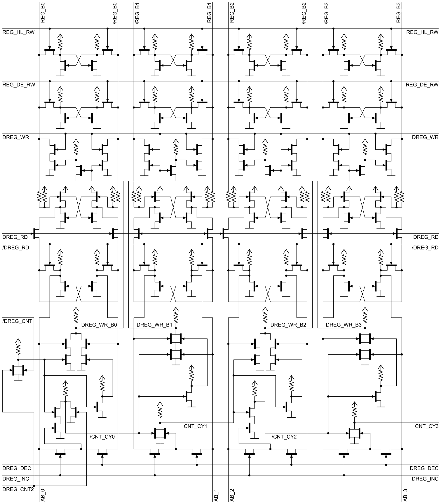
The circuit for the K and V flags

The following schematic shows the reverse-engineered circuit for the K and V flags in the 8085. The V flag is simply the exclusive-or of the carry into the top bit and the carry out of the top bit. This is a standard formula for computing overflow[2] for signed addition and subtraction. (The 6502 computes the same overflow value through different logic.) The V flag has values for other arithmetic operations, but the values aren't useful.[4] A latch stores the value of the V flag. The computed V value is stored in the latch under the control of a store_v_flag control signal. Alternatively, the flag value can be read off the bus and stored in the latch under the control of the bus_to_flags control signal; this is how the POP PSW instruction, which pops the flags from the stack, is implemented. Finally, a tri-state superbuffer (the large triangle) writes the flag value to the bus when needed.

The K flag circuitry is on the right. The first function of the K flag is overflow/underflow for an INX/DEX instruction. This is implemented simply: the carry_to_k_flag control line sets the K flag according to the carry from the incrementer/decrementer. The next function of K flag is reading from the databus for the POP PSW instruction, which is the same as for the V flag. The final function of the K flag is the result of a signed comparison. The K flag is the exclusive-or of the V flag and the sign bit of the result. For subtraction and comparison, the K flag is 1 if the second value is larger than the first.[5] The K flag is set for other arithmetic operations, but doesn't have a useful value except for signed comparison and subtraction.[4]

The circuit in the 8085 for the undocumented V and K flags. The flags are generated from the carries and results from the ALU. The K flag can also be set by the carry from the incrementer/decrementer.

The circuit in the 8085 for the undocumented V and K flags. The flags are generated from the carries and results from the ALU. The K flag can also be set by the carry from the incrementer/decrementer.
One mystery was the purpose of the K flag: "It does not resemble any normal flag bit."[1] Its use for increment and decrement is clear, but for arithmetic operations why would you want the exclusive-or of the overflow and sign? It turns out the the K flag is useful for signed comparisons. If you're comparing two signed values, the first is smaller if the exclusive-or of the sign and overflow is 1.[6] This is exactly what the K flag computes.

From the circuit above, it is clear that the V and K flags were deliberately added to the chip. (This is in contrast to the 6502, where undocumented opcodes have arbitrary results due to how the circuitry just happens to work for unexpected inputs.[7]) Why would Intel add the above circuitry to the chip and then not document or support it? My theory is that Intel decided they didn't want to support K or (8-bit) V flags in the 8086, so in order to make the 8086 source-compatible with the 8085, they dropped those flags from the 8085 documentation, but the circuitry remained in the chip.

The silicon

The 8085 microprocessor showing the data bus, ALU, flag logic, registers, and incrementer/decrementer.
The remainder of this article will show how the V and K flag circuits work, diving all the way down to the silicon circuits. The above image of the 8085 chip shows the layout of the chip and the components that are important to the discussion. In the upper left of the chip is the ALU (arithmetic-logic unit), where computations happen (details). The data bus is the main interconnect in the chip, connects the data pins (upper left), the ALU, the data registers, the flag register, and the instruction decoding (upper right). In the lower left of the chip is the 16-bit register file. Underneath the register file is a 16-bit increment/decrement circuit which handles incrementing the program counter, as well as supporting 16-bint increment and decrement instructions. The increment/decrement circuit has a carry-out in the lower right corner - this will be important for the discussion of the K flag. For some reason, the ALU has the low-order bit on the right, while the registers have the low-order bit on the left.

The flag logic circuitry sits underneath the ALU, with high-current drivers right on top of the data bus. The flags are arranged in apparently-random order with bit 7 (sign) on the left and bit 6 (zero) on the right. Because the carry logic is much more complicated (handling not only arithmetic operations but shifts and rotates, carry complement, and decimal adjust), the carry logic is stuck off to the right of the ALU where there was enough room.

Zooming in

Next we will zoom in on the V flag circuitry, labeled V1 above. Looking at the die under a microscope shows the metal layer of the chip, consisting of mostly-horizontal metal interconnects, which are the white lines below. The bottom part of the chip has the 8-bit data bus. Other wires are the VCC power supply, ground, and a variety of signals. While modern processors can have ten or more metal layers, the 8085 only has a single layer. Some of the circuitry underneath the metal is visible.

The metal layer of the 8085 microprocessor, zoomed in on the V flag circuit.

The metal layer of the 8085 microprocessor, zoomed in on the V flag circuit.
If the metal is removed from the chip, the silicon layer becomes visible. The blotchy green/purple is plain silicon. The pink regions are N-type doped silicon. The grayish regions are polysilicon, which can be considered as simply conductive wires. When polysilicon crosses doped silicon, it forms a transistor, which appears light green in this image. Note that transistors form a fairly small portion of the chip; there is a lot more connection and wiring than actual transistors. The small squares are vias, connections to the metal layer.

The V flag circuit in the 8085 CPU. This is the silicon/polysilicon after the metal layer has been removed. The data bus is not visible as it is in the metal layer, but it is in the lower third of the image. The rectangles at the bottom connect the data bus to the registers.

The V flag circuit in the 8085 CPU. This is the silicon/polysilicon after the metal layer has been removed. The data bus is not visible as it is in the metal layer, but it is in the lower third of the image. The rectangles at the bottom connect the data bus to the registers.

MOSFET transistors

For this discussion, a MOSFET can be considered simply a switch that closes if the gate input is 1 and opens if the gate input is 0. A MOSFET transistor is implemented by separating two diffusion regions, and putting a polysilicon wire over the gate. An insulating layer prevents any current from flowing between the gate and the rest of the transistor. In the following diagram, the n+ diffusion regions are pink, the polysilicon gate conductor is dull green, and the insulating oxide layer is turquoise.

Structure of a MOSFET transistor. The n+ diffusion regions are pink, the polysilicon gate conductor is dull green, and the insulating oxide layer is turquoise.

NOR gate

The NOR gate is a fundamental building block in the 8085, since it is a very simple gate that can form more complex logic. A NOR gate is implemented through two transistors and a pullup transistor. If either input (or both) is 1, the corresponding transistor connects the output to ground. Otherwise, the transistors are open, and the pullup pulls the output high. The pullup is shown as a resistor in the schematic, but it is actually a type of transistor called a depletion-mode transistor for better performance.

A NOR gate is implemented through two transistors and a pullup transistor. If either (or both) input is 1, the corresponding transistor connects the output to ground. Otherwise, the transistors are open, and the pullup pulls the output high.

By zooming in to a single NOR gate in the 8085, we can see how the gate is actually implemented. One surprise is that the circuit is almost all wiring; the transistors form a very small part of the circuit. The two transistors are connected to ground on the left, and tied together on the right. The pullup transistor is much larger than the other transistors for technical reasons.[8]

To understand the circuit, trace the path from ground to each transistor, across the gate, and to the output. In this way you can see there are two paths from ground to the output, and if either input is 1 the output will be 0.

The layout of the gate is intended to be as efficient as possible, given the constraints of where the power (VCC), ground, and other connections are, yielding a layout that looks a bit unusual. The power, ground, and input signals are all in the metal layer above (not shown here), and are connected to this circuit through vias between the metal and the silicon below.

A NOR gate in the 8085 microprocessor, showing the components.If either input is high, the associated transistor will connect the output to ground. Otherwise the pullup transistor will pull the output high.

A NOR gate in the 8085 microprocessor, showing the components.If either input is high, the associated transistor will connect the output to ground. Otherwise the pullup transistor will pull the output high.

Exclusive-or gates

The exclusive-or circuit (which outputs a 1 if exactly one input is 1) is a key component of the flag circuitry, and illustrates how more complex logic can be formed out of simpler gates. The schematic below shows how the exclusive-or is built from a NOR gate and an AND-NOR gate; it is straightforward to verify that if both inputs are 0 or both inputs are 1, the output is will be 0.

You may wonder why the 8085 uses so many "strange" gates such as a combined AND-NOR, instead of "normal" gates like AND. The transistor-level schematic shows that an AND-NOR gate can actually be implemented very simply with MOSFETs, in fact simpler than a plain AND gate. The two rightmost transistors form the "AND" - if they both have 1 inputs, they connect the output to ground. The transistor to the left forms the other part of the NOR - if it has a 1 input, it pulls the output to ground.

The exclusive-or circuit used in the 8085: gate-level and transistor-level.

The following diagram shows an XOR circuit in the 8085 that matches the schematic above. (This is the XOR gate that generates the K flag.) On the left is the NOR gate discussed above, and on the right is the AND-NOR circuit, both outlined with a dotted line. As before, the circuit is mostly wiring, with the transistors forming a small part of the circuit (the green regions between pink diffusion regions).

An XOR gate in the 8085 microprocessor, formed from a NOR gate and an AND-NOR gate. If both inputs are 0, the NOR gate output will be 1, and the NOR transistor will pull the output to 0. If both inputs are 1, the AND transistors will pull the output to 0. Otherwise the pullup transistor will pull the output 1.

An XOR gate in the 8085 microprocessor, formed from a NOR gate and an AND-NOR gate. If both inputs are 0, the NOR gate output will be 1, and the NOR transistor will pull the output to 0. If both inputs are 1, the AND transistors will pull the output to 0. Otherwise the pullup transistor will pull the output 1.

The flag latch

Each flag bit is stored in a simple latch circuit made up of two inverters. To store a 1, the inverter on the right outputs a 0, which is fed into the inverter on the left, which outputs a 1, which is fed back to the inverter on the right. A zero is stored in a similar (but opposite) manner. When the clock input is low, the pass transistor opens, breaking the feedback loop, and new data can be written into the latch. The complemented output (/out) is taken from the inverter.

You might wonder why the latch doesn't lose its data whenever the clock goes low. There's an interesting trick here called dynamic logic. Because the gate of a MOSFET consists of an insulating layer it has very high resistance. Thus, any electrical charge on the gate will remain there for some time[9] when the pass transistor opens. When the pass transistor closes, the charge is refreshed.

The latch used in the 8085 to store a flag value. The latch uses two inverters to store the data. When the clock is low, a new value can be written to the latch.

The latch used in the 8085 to store a flag value. The latch uses two inverters to store the data. When the clock is low, a new value can be written to the latch.

The following part of the 8085 chip shows the implementation of the latch for the V flag. The circuit closely matches the schematic above. The two inverters are outlined with dotted lines. The red arrows show the flow of data through the circuit. As before, the wiring and pullup transistors take up most of the silicon real estate.

Each flag in the 8085 uses a two-inverter latch to store the flag. This shows the latch for the undocumented V flag. The red arrows show the flow of data.

Each flag in the 8085 uses a two-inverter latch to store the flag. This shows the latch for the undocumented V flag. The red arrows show the flow of data.

Driving the data bus with a superbuffer

Another interesting feature of the flag circuit is the "superbuffer". Most transistors in the 8085 only send a signal a short distance. However, to send a signal on the data bus across the whole chip takes a lot more power, so a superbuffer is used. In the superbuffer, one transistor is driven to pull the output low, while a second transistor is driven to pull the output high. (This is in contrast to a regular gate, which uses a depletion-mode pullup transistor to pull the output high.) In addition, these transistors are considerably larger, to provide more current.[8] These two transistors are shown at the bottom the schematic below.

The other feature of this superbuffer is that it is tri-state. In addition to a 0 or 1 output, it has a third state, which basically consists of providing no output. This way, the flags do not affect the data bus except when desired. In the schematic, it can be seen that if the control input is 1, both NOR gates will output 0, and both transistors will do nothing.

The superbuffer used in the 8085 to drive the data bus.

The superbuffer used in the 8085 to drive the data bus.

The following diagram shows the two drive transistors, as well as the line used to read the flag from the data bus. (The NOR gates are not shown.) Note the size of these transistors compared to transistors seen earlier. Each flag bit requires a superbuffer such as this. Even flag bit 3, which is always 0, requires a large transistor to drive the 0 onto the bus - it's surprising that a do-nothing flag still takes up a fair bit of silicon.

Each flag in the 8085 uses a superbuffer to drive the value onto the data bus. This figure shows the two large transistors that drive the V flag onto bit 1 of the data bus.

Each flag in the 8085 uses a superbuffer to drive the value onto the data bus. This figure shows the two large transistors that drive the V flag onto bit 1 of the data bus.

Putting it all together

The above discussion has shown the details of the XOR gate that computes the K flag, and the latch and superbuffer for the V flag. The following diagram shows how these pieces fit into the overall circuitry. The latch and driver for the K flag are outside this image, to the right. The circuits below are tied together by the metal layer, which isn't shown. Compare this diagram with the schematic at the top of the article to see how the components are implemented. The two XOR circuits look totally different, since their layouts have been optimized to fit with the signals they need.

The 8085 circuits to implement the undocumented V and K flags. The ALU provides /carry6, /carry7, and result7. The XOR circuit on the left generates V, and the XOR circuit in the middle generates K. On the right are the latch for the V flag, and the superbuffer that outputs the flag to the data bus. The K flag latch and superbuffer are to the right, not shown.

The 8085 circuits to implement the undocumented V and K flags. The ALU provides /carry6, /carry7, and result7. The XOR circuit on the left generates V, and the XOR circuit in the middle generates K. On the right are the latch for the V flag, and the superbuffer that outputs the flag to the data bus. The K flag latch and superbuffer are to the right, not shown.
By looking at the silicon chip carefully, the transistors, gates, and complex circuits start to make sense. It's amazing to think that the complex computers we use are built out of these simple components. Of course, processors now are way more complex than the 8085, with billions of transistors instead of thousands, but the basic principles are still the same.

If you found this discussion interesting, check out my earlier analysis of the 6502's overflow flag and the 8085's ALU. You may also be interested in the book The Elements of Computing Systems, which describes how to build a computer starting with Boolean logic.

Credits

The chip images are from visual6502.org. The visual6502 team did the hard work of dissolving chips in acid to remove the packaging and then taking many close-up photographs of the die inside. Pavel Zima converted these photographs into mask layer images, a transistor net, and an 8085 simulator.

Notes and references

[1] The undocumented instructions and flags of the 8085 were discovered by Wolfgang Sehnhardt and Villy M. Sorensen in the process of writing an 8085 assembler, and were written up in the article Unspecified 8085 op codes enhance programming, Engineer's Notebook, "Electronics" magazine, Jan 18, 1979 p 144-145.

[2] See my article The 6502 overflow flag explained mathematically for details on overflow. There are multiple ways of computing overflow, and the 6502 uses a different technique.

[3] Tundra Semiconductor sold the CA80C85B, a CMOS version of the 8085. Interestingly, the undocumented opcodes and flags are described in the datasheet for this part: CA80C85B datasheet, 8000-series components.

The interesting thing about the Tundra datasheet is the descriptions of the "new" flags and instructions are copied almost exactly from Dehnhardt's article except for the introduction of errors, missing parentheses, and renaming the K flag as UI. In addition, as I described earlier, the published K/UI flag formula doesn't always work. Thus, it appears that despite manufacturing the chip, Tundra didn't actually know how these circuits worked.

[4] The V flag makes sense for signed addition and subtraction, and the K flag makes sense for signed subtraction and comparison. Many other operations affect these flags, but the flags may not have any useful meaning.

The V flag is 0 for RRC, RAR, AND, OR, and XOR operations, since these operations have constant carry values inside the ALU (details). The RLC and RAL operations add the accumulator to itself, so they can be treated the same as addition: V is set if the signed result is too big for a byte. The V flag for DAA can also be understood in terms of the underlying addition: V will only be set if the top digit goes from 7 to 8. However, since BCD digits are unsigned, V has no useful meaning with DAA. DAD is an interesting case, since the V flag indicates 16-bit signed overflow; it is actually computed from the result of the high-order addition. For INR, the only overflow case is going from 0x7f to 0x80 (127 to -128); note that going from 0xff to 0x00 corresponds to -1 to 0, which is not signed overflow even though it is unsigned overflow. Likewise, DCR sets the V flag going from hex 80 to 7f (-128 to 127); likewise 0x00 to 0xff is not signed overflow.

The K flag has a few special cases. For AND, OR, and XOR, the K flag is the same as the sign, since the V flag is 0. Note that the K flag is computed entirely differently for INR/DCR compared to INX/DCX. For INR and DCR, the K flag is S^V, which almost always is S. The K flag is set for DAA if S^V is true, which doesn't have any useful meaning since BCD values are unsigned.

The published formula for the K flag gives the wrong value for XOR if both arguments are negative.

[5] The following table illustrates the 8 possible cases when comparing signed numbers A and B. The inputs are the top bit of A, the top bit of B, and the carry from bit 6 when subtracting B from A. The outputs are the carry, borrow (complement of carry), sign, overflow, and K flags. An example is given for each row. Note that the K flag is set if A is less than B when treated as signed numbers.

InputsOutputsExample
A7B7C6CBSVKHexSigned comparison
010010000x50 - 0xf0 = 0x6080 - -16 = 96
011011100x50 - 0xb0 = 0xa080 - -80 = -96
000011010x50 - 0x70 = 0xe080 - 112 = -32
001100000x50 - 0x30 = 0x12080 - 48 = 32
110011010xd0 - 0xf0 = 0xe0-48 - -16 = -32
111100000xd0 - 0xb0 = 0x120-48 - -80 = 32
100100110xd0 - 0x70 = 0x160-48 - 112 = 96
101101010xd0 - 0x30 = 0x1a0-48 - 48 = -96

[6] A detailed explanation of signed comparisons is given in Beyond 8-bit Unsigned Comparisons by Bruce Clark, section 5. While this article is in the context of the 6502, the discussion applies equally to the 8085.

[7] The illegal opcodes in the 6502 are discussed in detail in How MOS 6502 Illegal Opcodes really work. In the 6502, the operations performed by illegal opcodes are unintended, just chance based on what the chip logic happens to do with unexpected inputs. In contrast, the undocumented opcodes in the 8085, like the undocumented flags, are deliberately implemented.

[8] The key parameter in the performance of a MOSFET transistor is the width to length ratio of the gate. Oversimplifying slightly, the current provided by the transistors is proportional to this ratio. (Width is the width of the source or drain, and length is the length across the gate from source to drain.) For an inverter, the W/L ratio of the pullup should be approximately 1/4 the W/L ratio of the input transistor for best performance. (See Introduction to VLSI Systems, Mead, Conway, p 8.) The result is that pullup transistors are big and blocky compared to pulldown transistors. Another consequence is that high-current transistors in a superbuffer have a very wide gate. The 8085 register file has some transistors where the W/L ratios are carefully configured so one transistor will "win" over the other if both are on at the same time. (This is why the 8085 simulator is more complex than the 6502 simulator, needing to take transistor sizes into account.)

[9] One effect of using pass-transistor dynamic buffers is that if the clock speed is too small, the charge will eventually drain away causing data loss. As a result the 8085 has a minimum clock speed of 500 kHz. Likewise, the 6502 has a minimum clock speed. The Z-80 in contrast is designed with static logic, so it has no minimum clock speed - the clock can be stepped as slowly as desired.