The new biography
Steve Jobs contains a remarkable claim about the power supply of the Apple II and its designer Rod Holt:
[1]
Instead of a conventional linear power supply, Holt built one like those used in oscilloscopes. It switched the power on and off not sixty times per second, but thousands of times; this allowed it to store the power for far less time, and thus throw off less heat. "That switching power supply was as revolutionary as the Apple II logic board was," Jobs later said. "Rod doesn't get a lot of credit for this in the history books but he should. Every computer now uses switching power supplies, and they all rip off Rod Holt's design."
I found it amazing to think that computers now use power supplies based on the Apple II's design, so I did some investigation. It turns out that Apple's power supply was not revolutionary, either in the concept of using a switching power supply for computers or in the specific design of the power supply.
Modern computer power supplies are totally different and do not rip off anything from Rod Holt's design. It turns out that Steve Jobs was making his customary claim that everyone is stealing Apple's revolutionary technology, entirely contrary to the facts.
The history of switching power supplies turns out to be pretty interesting. While most people view the power supply as a boring metal box, there's actually a lot of technological development behind it. There was, in fact, a revolution in power supplies in the late 1960s through the mid 1970s as switching power supplies took over from simple but inefficient linear power supplies, but this was a few years before the Apple II came out in 1977. The credit for this revolution should go to advances in semiconductor technology, specifically improvements in switching transistors, and then innovative ICs to control switching power supplies.[2]
Some background on power supplies
In a standard desktop computer, the power supply converts AC line voltage into DC, providing several carefully regulated low voltages at high currents. Power supplies can be built in a variety of ways, but linear and switching power supplies are the two techniques relevant to this discussion. (See the notes for more about obsolete technologies such as large
mechanical motor-generator systems
[3] and ferroresonant transformers
[4][5].)
A typical linear power supply uses a bulky power transformer to convert the 120V AC into a low AC voltage, converts this to low voltage DC with a diode bridge, and then uses a linear regulator to drop the voltage to the desired level. The linear regulator is an inexpensive easy-to-use transistor-based component that turns the excess voltage into waste heat to produce a stable output. Linear power supplies are almost trivial to design and build.[6] One big disadvantage however, is they typically waste about 50-65% of the power as heat,[7] often requiring large metal heat sinks or fans to get rid of the heat. The second disadvantage is they are large and heavy. On the plus side, the components (other than the transformer) in linear power supplies only need to handle low voltages and the output is very stable and noise-free.
A switching power supply works on a very different principle: rapidly turning the power on and off, rather than turning excess power into heat. In a switching power supply, the AC line input is converted to high-voltage DC, and then the power supply switches the DC on and off thousands of times a second, carefully controlling the time of the switching so the output voltage averages out to the desired value. Theoretically, no power gets wasted, although in practice the efficiency will be 80%-90%. Switching power supplies are much more efficient, give off much less heat, and are much smaller and lighter than linear power supplies.
The main disadvantage of a switching power supply is it is considerably more complex than a linear power supply and much harder to design.[8] In addition, it is much more demanding on the components, requiring transistors that can efficiently switch on and off at high speed under high power. The switches, inductors, and capacitors in a switching power supply can be arranged in several different arrangements (or topologies), with names such as Buck, Boost, Flyback, Forward, Push-Pull, Half Wave, and Full-Wave.[9]
History of switching power supplies to 1977
Switching power supply principles were known since the 1930s
[6] and were being built out of discrete components in the 1950s.
[10] In 1958, the IBM 704 computer used a primitive vacuum-tube based switching regulator.
[11] The company Pioneer Magnetics started building switching power supplies in 1958
[12] (and decades later made a key innovation in PC power supplies
[13]). General Electric published an early switching power supply design in 1959.
[14] In the 1960s the aerospace industry and NASA
[15] were the main driving force behind switching power supply development, since the advantages of small size and high efficiency made up for the high cost.
[16] For example, NASA used switching supplies for satellites
[17][18] such as Telstar in 1962.
[19]
The computer industry started using switching power supplies in the late 1960s and they steadily grew in popularity.
Examples include the PDP-11/20 minicomputer in 1969,[20] the Honeywell H316R in 1970,[21] and Hewlett-Packard's 2100A minicomputer in 1971.[22][23]
By 1971, companies using switching regulators "read like a 'Who's Who' of the computer industry: IBM, Honeywell, Univac, DEC, Burroughs, and RCA, to name a few."[21]
In 1974, HP used a switching power supply for the 21MX minicomputer,[24] Data General for the Nova 2/4,[25] Texas Instruments for the 960B,[26] and Interdata for their minicomputers.[27]
In 1975, HP used an off-line switching power supply in the HP2640A display terminal,[28] Matsushita for their traffic control minicomputer,[29] and IBM for its typewriter-like Selectric Composer[29] and for the IBM 5100 portable computer.[30]
By 1976, Data General was using switching supplies for half their systems, Hitachi and Ferranti were using them,[29] Hewlett-Packard's 9825A Desktop Computer[31] and 9815A Calculator[32] used them, and the decsystem 20[33] used a large switching power supply. By 1976, switching power supplies were showing up in living rooms, powering color television receivers.[34][35]
Switching power supplies also became popular products for power supply manufacturers starting in the late 1960s.
In 1967, RO Associates introduced the first 20Khz switching power supply product,[36] which they claim was also the first switching power supply to be commercially successful.[37] NEMIC started developing standardized switching power supplies in Japan in 1970.[38]
By 1972, most power supply manufacturers were offering switching power supplies or were about to offer them.[5][39][40][41][42]
HP sold a line of 300W switching power supplies in 1973,[43] and a compact 500W switching power supply[44] and a 110W fanless switching power supply[45] in 1975. By 1975, switching power supplies were 8% of the power supply market and growing rapidly, driven by improved components and the desire for smaller power supplies for products such as microcomputers.[46]
Switching power supplies were featured in electronics magazines of this era, both in advertisements and articles.
Electronic Design recommended switching power supplies in 1964 for better efficiency.[47]
The October 1971 cover of Electronics World featured a 500W switching power supply and an article "The Switching Regulator Power Supply".
A long article about power supplies in Computer Design in 1972 discussed switching power supplies in detail and the increasing use of switching power supplies in computers, although it mentions some companies were still skeptical about switching power supplies.[5]
In 1973, Electronic Engineering featured a detailed article "Switching power supplies: why and how".[42]
In 1976, the cover of Electronic Design[48] was titled "Suddenly it's easier to switch" describing the new switching power supply controller ICs,
Electronics ran a long article on switching power supplies,[29]
Powertec ran two-page ads on the advantages of their switching power supplies with the catchphrase "The big switch is to switchers",[49] and Byte magazine announced Boschert's switching power supplies for microcomputers.[50]
A key developer of switching power supplies was Robert Boschert, who quit his job and started building power supplies on his kitchen table in 1970.[51] He focused on simplifying switching power supplies to make them cost-competitive with linear power supplies, and by 1974 he was producing low-cost power supplies in volume for printers,[51][52] which was followed by a low-cost 80W switching power supply in 1976.[50] By 1977 Boschert Inc had grown to a 650-person company[51] that producing power supplies for satellites and the F-14 fighter aircraft,[53] followed by power supplies for companies such as HP[54] and Sun.
People often think of the present as a unique time for technology startups, but Boschert illustrates that kitchen-table startups were happening even 40 years ago.
The advance of the switching power supply during the 1970s was largely driven by new components.[55]
The voltage rating of switching transistors was often the limiting factor,[5] so the introduction of high voltage, high speed, high power transistors at a low cost in the late 1960s and early 1970s greatly increased the popularity of switching power supplies.[5][6][21][16]
Transistor technology moved so fast that a 500W commercial power supply featured on the cover of Electronics World in 1971 couldn't have been built with the transistors of just 18 months earlier.[21]
Once power transistors could handle hundreds of volts, power supplies could eliminate the heavy 60 Hz power transformer and run "off-line" directly from line voltage. Faster transistor switching speeds allowed more efficient and much smaller power supplies.
The introduction of integrated circuits to control switching power supplies in 1976 is widely viewed as ushering in the age of switching power supplies by drastically simplifying them.[10][56]
By the early 1970s, it was clear that a revolution was taking place. Power supply manufacturer Walt Hirschberg claimed in 1973 that "The revolution in power supply design now under way will not be complete until the 60-Hz transformer has been almost entirely replaced."[57] In 1977, an influential power supply book said that "switching regulators were viewed as in the process of revolutionizing the power supply industry".[58]
The Apple II and its power supply
The Apple II personal computer was introduced in 1977. One of its features was a compact, fanless switching power supply, which provided 38W of power at 5, 12, -5, and -12 volts. Holt's Apple II power supply uses a very simple design, with an off-line flyback converter topology.
[59]
Steve Jobs said that every computer now rips off Rod Holt's revolutionary design.[1] But is this design revolutionary? Was it ripped off by every other computer?
As illustrated above, switching power supplies were in use by many computers by the time the Apple II was released. The design is not particularly revolutionary, as similar simple off-line flyback converters were being sold by Boschert[50][60] and other companies. In the long term, building the control circuitry out of discrete components as Apple did was a dead-end technology, since the future of switching power supplies was in PWM controller ICs.[2] It's surprising Apple continued using discrete oscillators in power supplies even through the Macintosh Classic, since IC controllers were introduced in 1975.[48] Apple did switch to IC controllers, for instance in the Performa[61] and iMacs.[62]
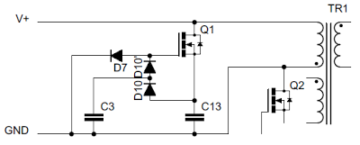
The power supply that Rod Holt designed for Apple was innovative enough to get a patent,[63] so I examined the patent in detail to see if there were any less-obvious revolutionary features. The patent describes two mechanisms to protect the power supply against faults. The first (claim 1) is a mechanism to safely start the oscillator through an AC input. The second mechanism (claim 8) returns excess energy from the transformer to the power source (especially if there is no load) through a clamp winding on the transformer and a diode.

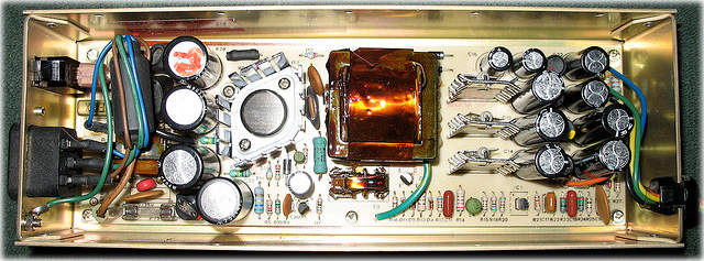
This is the AA11040-B power supply for the Apple II Plus.
[59] AC power enters, on the left, is filtered, goes through the large switching transistor to the flyback transformer in the middle, is rectified by the diodes to the right (on heatsinks), and then is filtered by the capacitors on the right. The control circuitry is along the bottom. Photo used by permission from kjfloop, Copyright 2007.
The AC start mechanism was not used by the Apple II,[59] but was used by the Apple II Plus,[64] Apple III,[65] Lisa,[66] Macintosh,[67] and Mac 128K through Classic.[68] I could not find any non-Apple power supplies that use this mechanism,[69] except for a 1978 TV power supply,[70] and it became obsoleted by IC controllers, so this mechanism seems to have had no impact on computer power supply design.
The second mechanism in Holt's patent, the clamp winding and diode to return power in a flyback converter, was used in a variety of power supplies until the mid-1980s and then disappeared.
Some examples are the Boschert OL25 power supply (1978),[60]
Apple III (1980),[65]
Apple's power supply documentation (1982),[59]
Tandy hard drive (1982),[71]
Tandy 2000 (1983),[72][73]
Apple Lisa (1983),[66]
Apple Macintosh (1984),[67]
Commodore Model B128 (1984),[74]
Tandy 6000 (1985),[75]
and
Mac Plus (1986) to Mac Classic (1990).[68]
This flyback clamp winding seems to have been popular with Motorola in the 1980s, appearing in the MC34060 controller IC datasheet,[76] a 1983 designer's guide[77] (where the winding was described as common but optional), and a 1984 application note.[78]
Is this flyback clamp winding the innovation of Holt's that other companies ripped off? I thought so, until I found a 1976 power supply book that described this winding in detail,[35] which ruined my narrative. (Also note that forward converters (as opposed to flyback converters) had used this clamp winding dating back to 1956,[79][80][81] so applying it to a flyback converter doesn't seem like a huge leap in any case.)
One puzzling aspect of power supply discussion in the book Steve Jobs[1] is the statement that the Apple II's power supply is "like those used in oscilloscopes", since oscilloscopes are just one small use for switching power supplies. This statement apparently arose because Holt had previously designed a switching power supply for oscilloscopes,[82] but there's no other connection between Apple's power supply and oscilloscope power supplies.
The biggest impact of the Apple II on the power supply industry was on Astec - the Hong Kong company that manufactured the power supply. Before the Apple II came out, Astec was a little-known manufacturer, selling switching DC-DC inverters. But by 1982, Astec had become the world's top switching-powers-supply manufacturer, almost entirely based on Apple's business, and kept the top spot for a number of years.[83][84] In 1999, Astec was acquired by Emerson,[85] which is currently the second-largest power supply company after Delta Electronics.[86]
A little-known fact about the Apple II power supply is that it was originally assembled by middle-class California housewives as piecework.[83] As demand grew, however, power supply construction was transferred to Astec, even though it cost $7 a unit more. Astec was building 30,000 Apple power supplies monthly by 1983.[83]
Power supplies post-Apple
In 1981, the IBM PC was launched, which would have lasting impact on computer power supply designs. The power supply for the original IBM 5150 PC was produced by Astec and Zenith.
[83] This 63.5W power supply used a flyback design controlled by a NE5560 power supply controller IC.
[87]
I will compare the IBM 5150 PC power supply with the Apple II power supply in detail to show their commonalities and differences. They are both off-line flyback power supplies with multiple outputs, but that's about all they have in common. Even though the PC power supply uses an IC controller and the Apple II uses discrete components, the PC power supply uses approximately twice as many components as the Apple II power supply. While the Apple II power supply uses a variable frequency oscillator built out of transistors, the PC power supply uses a fixed-frequency PWM oscillator provided by the NE5560 controller IC. The PC uses optoisolators to provide voltage feedback to the controller, while the Apple II uses a small transformer. The Apple II drives the power transistor directly, while the PC uses a drive transformer. The PC checks all four power outputs against lower and upper voltage limits to make sure the power is good, and shuts down the controller if any voltages are out of spec. The Apple II instead uses a SCR crowbar across the 12V output if that voltage is too high. While the PC flyback transformer has a single primary winding, the Apple II uses an extra primary clamp winding to return power, as well as another primary winding for feedback. The PC provides linear regulation on the 12V and -5V supplies, while the Apple II doesn't. The PC uses a fan, while the Apple II famously doesn't. It's clear that the IBM 5150 power supply does not "rip off" the Apple II power supply design, as they have almost nothing in common. And later power supply designs became even more different.
The IBM PC AT power supply became a de facto standard for computer power supplies. In 1995, Intel introduced the ATX motherboard specification,[88] and the ATX power supply (along with variants) has become the standard for desktop computer power supplies, with components and designs often targeted specifically at the ATX market.[89]
Computer power systems became more complicated with the introduction of the voltage regulator module (VRM) in 1995 for the Pentium Pro, which required lower voltage at higher current than the power supply could provide directly. To supply this power, Intel introduced the VRM - a DC-DC switching regulator installed next to the processor that reduces the 12 volts from the power supply to the low voltage used by the processor.[90] (If you overclock your computer, it is the VRM that lets you raise the voltage.) In addition, graphics cards can have their own VRM to power a high-performance graphics chip. A fast processor can require 130 watts from the VRM. Comparing this to the half watt of power used by the Apple II's 6502 processor[91] shows the huge growth in power consumption by modern processors. A modern processor chip alone can use more than twice the power of the whole IBM 5150 PC or three times that of the Apple II.
The amazing growth of the computer industry has caused the power consumption of computers to be a cause for environmental concern, resulting in initiatives and regulations to make power supplies more efficient.[92] In the US, Energy Star and 80 PLUS certification[93] pushes manufacturers to manufacture more efficient "green" power supplies.
These power supplies squeeze out more efficiency through a variety of techniques: more efficient standby power, more efficient startup circuits, resonant circuits (also known as soft-switching and ZCT or ZVT) that reduce power losses in the switching transistors by ensuring that no power is flowing through them when they turn off, and "active clamp" circuits to replace switching diodes with more efficient transistor circuits.[94] Improvements in MOSFET transistor and high-voltage silicon rectifier technology in the past decade has also led to efficiency improvements.[92]
Power supplies can use the AC line power more efficiently through the technique of power factor correction (PFC).[95] Active power factor correction adds another switching circuit in front of the main power supply circuit. A special PFC controller IC switches this at a frequency of up to 250kHZ, carefully extracting a smooth amount of power from the power supply to produce high-voltage DC, which is then fed into a regular switching power supply circuit.[13][96] PFC also illustrates how power supplies have turned into a commodity with razor-thin margins, where a dollar is a lot of money. Active power factor correction is considered a feature of high-end power supplies, but its actual cost is only about $1.50.[97]
Many different controller chips, designs, and topologies have been used for IBM PC power supplies over the years, both to support different power levels, and to take advantage of new technologies.[98] Controller chips such as the NE5560 and SG3524 were popular in early IBM PCs.[99] The TL494 chip became very popular in a half-bridge configuration,[99] the most popular design in the 1990s.[100] The UC3842 series was also popular for forward converter configurations.[99]
The push for higher efficiency has made double forward converters more popular,[101] and power factor correction (PFC) has made the CM6800 controller very popular,[102] since the one chip controls both circuits. Recently, forward converters that generate only 12V have become more common, using DC-DC converters to produce very stable 3.3V and 5V outputs.[94]
More detailed information on modern power supplies is available from many sources.[103][104][98][105]

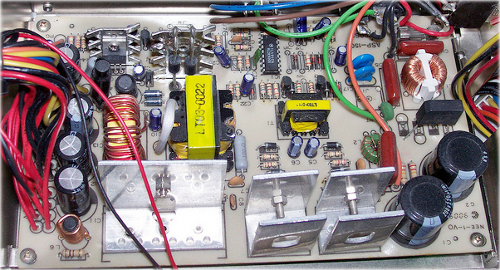
This typical 150W XT power supply uses the popular half-bridge design. The AC input filtering is on the right. To the left of this is the control/driver circuit: the TL494 IC at the top controls the small yellow drive transformer below, which drives the two switching transistors on the heatsinks below. To the left of this is the larger yellow main transformer, with the secondary diodes and regulator on the heatsinks, and output filtering to the left. This half-bridge power supply design is totally different from the Apple II's flyback design. Photo copyright larrymoencurly, used with permission.
Modern computers contain a surprising collection of switching power supplies and regulators. A modern power supply can contain a switching PFC circuit, a switching flyback power supply for standby power, a switching forward converter to generate 12 volts, a switching DC-DC converter to generate 5 volts, and a switching DC-DC converter to generate 3.3 volts,[94] so the ATX power supply can be considered five different switching power supplies in one box. In addition, the motherboard has a switching VRM regulator to power the processor, and the graphics card has another VRM, for a total of seven switching supplies in a typical desktop computer.
The technology of switching power supplies continues to advance. One development is digital control and digital power management.[106] Instead of using analog control circuits, digital controller chips digitize the control inputs and use software algorithms to control the outputs. Thus, designing the power supply controller becomes as much a matter of programming as of hardware design. Digital power management lets power supplies communicate with the rest of the system for higher efficiency and logging. While these digital technologies are largely used for servers now, I expect they will trickle down to desktop computers eventually.
To summarize, the original IBM 5150 PC power supply was different in almost every way from the Apple II power supply, except both were flyback power supplies. More recent power supplies don't even have that in common with the Apple II. It's absurd to claim that power supplies are ripping off Apple's design.
Famous switching power supply designers
Steve Jobs said that Rod Holt should be better known for designing the Apple II's power supply: "Rod doesn't get a lot of credit for this in the history books but he should."
[1]
But even at best, power supply designers aren't famous outside a very small community. Robert Boschert was inducted into Electronic Design's Electronic Engineering Hall of Fame in 2009 for his power supply work.
[51]
Robert Mammano got Power Electronics Technology's lifetime achievement award in 2005 for starting the PWM controller IC industry.
[10] Rudy Severns got Power Electronics Technology's lifetime achievement award in 2008 for his innovations in switching power supplies.
[107] But none of these people are even Wikipedia-famous. Other major innovators in the field get even less attention.
[108] I repeatedly came across the work of Elliot Josephson, who designed satellite power systems in the early 1960s
[18], has a bunch of power supply patents including the Tandy 6000
[75], and even has his patent number printed on the Apple II Plus and Osborne 1 power supply circuit boards
[59], but he appears to be entirely unrecognized.
The irony in Steve Jobs' comment that Rod Holt doesn't get a lot of credit is that Rod Holt's work is described in dozens of books and articles about Apple, from Revenge of the Nerds in 1982[109] to 2011's best-selling Steve Jobs biography, which makes Rod Holt easily the most famous power supply designer ever.
Conclusion
Power supplies aren't the boring metal boxes that most people think; they have a lot of interesting history, driven largely by the improvements in transistors that made switching power supplies practical for computers in the early 1970s. More recently, efficiency standards such as 80 PLUS have forced power supplies to become more efficient, resulting in new designs. The Apple II sold a huge number of switching power supplies, but its power supply design was a technological dead end that was not "ripped off" by other computers.
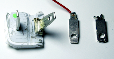
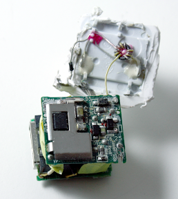
If you're interested in power supplies, you might also like my article Tiny, cheap, and dangerous: Inside a (fake) iPhone charger.
Notes and references
I spent way too much time researching power supplies, analyzing schematics and digging through old electronics journals. Here are my notes and references, in case they are of use to someone else. I'd be interested in hearing from power supply designers who have first-hand experience with the development of power supplies in the 1970s and 1980s.
[1]
Steve Jobs, Walter Isaacson, 2011. Rod Holt's power supply design for the Apple II is discussed on page 74. Note that the description of a switching power supply in this book is rather garbled.
[2]
PWM: From a Single Chip To a Giant Industry, Gene Heftman, Power Electronics Technology, pp48-53, Oct 2005.
[3]
Preliminary Site Planning: Cray-1 Computer (1975)
The Cray-1 used two 200 HP (150KW) motor-generator units to convert 250A 460V input AC into regulated 208V, 400Hz power; each motor-generator was approximately 3900 pounds. The 208V 400Hz power was fed into 36 separate power supplies that used twelve-phase transformers but no internal regulators. These power supplies famously formed the 12 benches around the Cray computer.
Photographs of the Cray power components are in Cray-1 S Series Hardware Reference Manual (1981).
This high-frequency motor-generator setup may seem strange, but the IBM 370 used a similar setup, see Announcing: IBM System/370 Model 145.
[4]
Many larger computers used ferroresonant transformers for regulation. For instance, the power supply for the IBM 1401 computer used a 1250W ferroresonant regulator, see Reference Manual, 1401 Data Processing System (1961), p13.
The HP 3000 Series 64/68/70 also used ferroresonant transformers, see Series 64/68/70 Computer Installation Manual (1986), p2-3. DEC used ferroresonant and linear power supplies almost exclusively in the early 1970s, including for the PDP-8/A (picture in "Power-supply choice looms large in sophisticated designs", Electronics, Oct 1976, volume 49, p111).
[5]
"Power Supplies for Computers and Peripherals", Computer Design, July 1972, pp 55-65. This long article on power supplies has a lot of discussion of switching power supplies. It describes the buck (series), boost (shunt), push-pull (inverter), and full bridge topologies. The article says that the voltage rating of the switching transistor is the limiting parameter in many applications, but "high voltage, high speed transistors are increasingly available at low cost - an important factor in the more widespread use of switching regulator supplies."
It concludes that "Availability of high voltage, high power, switching transistors at moderate prices is providing extra impetus to the use of high efficiency switching regular [sic] supplies. Substantial increase in usage is expected this year."
The article also says, "One of the more controversial topics is the continuing debate on the value of switching type supplies for computer applications, as contrasted with conventional series transistor regulators." This is echoed by some of the vendor comments. One skeptic was Elexon Power Systems, which "does not regard switching regulators as 'the answer.' They plan to disclose an entirely new power supply approach in the near future." Another was Modular Power Inc, who "recommend against switching regulators except when small size, light weight, and high efficiency are primary considerations, as in portable and airborne equipment." Sola Basic Industries said "their engineers are highly skeptical of the long term reliability of switching regulators in practical mass production designs, and predict transistor failure problems."
The "vendor comments" section of the article provides insight into the technology of the power supply industry in 1972:
Hewlett Packard "specifies that a major influence today is the ready availability of high speed, high current, low cost transistors accelerated by the current trend toward switching type regulators. The company makes extensive use of switching in a full range of high power designs."
Lambda Electronics "makes extensive use of switching regulators for outputs above about 100 W" which are designed to avoid fan cooling.
Analog Devices offered precision supplies that use switching techniques for high efficiency.
RO Associates "considers growth of switching power supplies to be a major change in the power supply design area". They offered miniature 20-kHz supplies, and low cost 60-kHz supplies.
Sola Basic Industries "predict that minicomputer manufacturers will be using more transformerless switching regulators in 1972, for high efficiency and reduced size and weight."
Trio Laboratories "indicates that computer and peripheral manufacturers are turning to switching types because pricing is now more competitive and applications are requiring reduced size."
[6]
Practical switching power supply design, Marty Brown, 1990, p17.
[7]
See the comment section for a detailed discussion of linear power supply efficiency.
[8]
Power Supply Cookbook, Marty Brown, 2001.
Page 5 discusses the relative development time for different power supply technologies, with a linear regulator taking 1 week of total development time, while a PWM switching regulator takes 8 person-months.
[9]
A summary of different topologies is in SMPS overview and Power Supply Topologies.
Details are in Microchip AN 1114: SMPS Topologies and
Topologies for switched mode power supplies
[10]
Lifetime Achievement Award Recipient Robert Mammano, Power Electronics Technology, Sep 2005, pp 48-51. This article describes the Silicon General SG1524 (1975) as the IC that ushered in the age of switching regulators and switch-mode power supplies.
[11]
IBM Customer Engineering Reference Manual: 736 Power Supply, 741 Power Supply, 746 Power Distribution Unit (1958), page 60-17. The power supply for the 704 computer consists of three refrigerator-sized cabinets full of vacuum tubes, fuses, relays, mechanical timers, and transformers, using 90.8KVA of power. It used multiple regulation techniques including saturable-reactor transformers and thermistor-based reference voltage. The DC outputs were regulated by a 60 Hz thyratron switching mechanism. Thyratrons are switching vacuum tubes that control the output voltage (much like TRIACs in a common dimmer switch). This can be considered a switching power supply (see Power supplies, switching regulators, inverters, and converters, Irving Gottlieb, pp 186-188).
[12]
In their ads, Pioneer Magnetics claims to have designed their first switching power supply in 1958. For instance, see Electronic Design, V27, p216.
[13]
Unity power factor power supply, patent 4677366. Pioneer Magnetics filed this patent in 1986 on active power factor correction.
See also Pioneer Magnetics' Why PFC? page.
[14]
An early switching power supply was described in
"A Transistor Power Converter-Amplifier", D. A. Paynter, General Electric Co.,
Solid-State Circuits Conference, 1959, p90-91.
Also see related 1960 patent 3067378, Transistor Converter.
[15]
Nondissipative DC to DC Regulator Converter Study, Goddard Space Flight Center, 1964. This survey of transistorized DC-DC converters shows about 20 different switching designs known in the early 1960s. The flyback converter is notably absent. Many other NASA reports on power converters from this time period are available from NASA Technical Reports Server.
[16]
A detailed history of switching power supplies appears in S.J. Watkins' M.Phil. thesis Automatic testing of switched-mode power supplies, in the chapter
History and Development of Switched-Mode Power Supplies Pre 1987.
[17]
Switching Power Supply Development History, TDK Power Electronics World. This provides a very brief history of switching power supplies. TDK also has a surprisingly detailed discussion of switching power supplies in comic form:
TDK Power Electronics World.
[18]
"Satellite power supply has variable pulse width",
Electronics, Feb 1962, p47-49. This article by Elliot Josephson of Lockheed describes a constant-frequency PWM DC-DC converter for satellites. See also patent 3219907 Power Conversion Device.
[19]
The Spacecraft Power Supply System, Telstar, 1963. The Telstar satellite obtained power from solar cells, storing the power in NiCad batteries. Efficiency was critical for the satellite, so a DC-to-DC switching voltage regulator was used, with a buck converter converting the variable battery voltage into stable -16 V DC at up to 32 watts at up to 92% efficiency. Because the satellite needed a wide range of voltages, up to 1770 volts for the RF amplifier, additional converters were used. The regulated DC was inverted to AC, fed into transformers, and rectified, to produce the required voltages.
[20]
Some PDP models, such as the PDP-11/20 used the H720 power supply (see PDP handbook, 1969). This power supply is described in detail in H720 Power Supply and Mounting Box Manual (1970). The 25 pound power supply uses a power transformer to generate 25V DC, and then switching switching regulators (buck converter) to generate 230W of regulated +5 and -15 volts. Because transistors of the era couldn't handle high voltages, the DC voltage had to be reduced to 25 volts by a large power transformer.
[21]
"The Switching Regulator Power Supply", Electronics World v86 October 1971, p43-47.
This long article on switching power supplies was featured on the cover of Electronics World. The article is worth looking up, if only for the picture of the F-111 aircraft's switching power supply, which looks so complex that I'd almost expect it to land the plane. The switching power supplies discussed in this article combine a switching DC-DC inverter with a transformer for isolation with a separate buck or boost switching regulator. As a result, the article claims that switching power supplies will always be more expensive than linear power supplies because of the two stages. Modern power supplies, however, combine both stages. The article discusses a variety of power supplies including the 250W switching power supply used by the Honeywell H316R. The article says that the switching regulator power supply had come of age because of new advances in high-speed and high-power transistors. The cover shows a 500W switching power supply that according to the article could not have been built with the transistors available just a year and a half earlier.
[22]
A Bantam Power Supply for a Minicomputer, Hewlett-Packard Journal, October 1971. Circuit details in High Efficiency Power Supply patent 3,852,655. This is a 492W off-line power supply using inverters followed by 20V switching regulators.
[23]
The HP2100A was introduced in 1971 with a switching power supply (see HP2100A Main Specifications). It is claimed to have the first switching power supply in a minicomputer 25 Years of Real-Time Computing, but the PDP-11/20 was earlier.
[24]
A Computer Power System for Severe Operating Conditions, p21, Hewlett-Packard Journal, Oct 1974.
The 21MX minicomputer used a 300 W, off-line, switching preregulator to generate regulated 160V DC which was fed into switching dc-to-dc converters.
[25]
Data General Technical Manual Nova 2, 1974. The Nova 2/4 used switching regulator to generate 5V and 15V, while the larger 2/10 used a constant voltage transformer. The manual says, "At the higher current losses associated with a computer, the losses [from linear regulators] may become excessive, and for this reason the switching regulator is often used, as in the NOVA 2/4."
[26]
Model 960B/980B Computer Maintenance Model: Power Supply
The power supply for the Texas Instruments 960B minicomputer used a switching regulator for the 150W 5V supply and linear regulators for the other voltages. The switching regulator consists of two parallel buck converters running at 60kHz, and using 2N5302 NPN switching transistors (introduced in 1969). Because the transistors have a 60V maximum rating, the power supply uses a transformer to drop the voltage to 35V that is fed into the regulator.
[27]
M49-024 and M49-026 Switching Regulated Power Supply Instruction Manual, Interdata, 1974. These off-line half-bridge power supplies provided 120W or 250W and were used by the Interdata minicomputers. The switching oscillator used 555 and 556 timer chips.
[28]
2640A Power Supply, Hewlett-Packard Journal, June 1975, p 15. "A switching mode power supply was chosen because of the efficiency and space requirement."
Also Data Terminal Technical Information.
Another point of interest is its case molded of structural foam (p23) which is very similar to the Apple II's foam-molded plastic case (see page 73 of Steve Jobs), and a couple years earlier.
[29]
"Power-supply choice looms large in sophisticated designs",
Electronics, Oct 1976, volume 49. p107-114. This long article discusses power supplies including switching power supplies in detail. Note that the Selectric Composer is very different from the popular Selectric typewriter.
[30]
IBM 5100 Portable Computer Maintenance Information Manual. The IBM 5100 was a 50-pound portable computer that used BASIC and APL, and included a monitor and tape drive. The power supply is described on page 4-61 as a small, high power, high frequency transistor switching regulator supply that provides 5V, -5V, 8.5V, 12V, and -12V.
[31]
The HP 9825A Desktop Computer from 1976 used a switching regulator for the 5V power supply. It also used a foam-molded case, predating the Apple II's; see 98925A Product Design, Hewlett-Packard Journal, June 1976, p5.
[32]
Mid-Range Calculator Delivers More Power at Lower Cost, Hewlett-Packard Journal, June 1976 discusses the 5V switching power supply used by the 9815A calculator.
[33]
DEC's H7420 power supply is described in decsystem 20 Power Supply System Description (1976). It holds 5 switching regulators to provide multiple voltages, and provides about 700 W. The power supply uses a large transformer to reduce the line voltage to 25V DC, which is passed to the individual switching regulators, which use a buck topology to obtain the desired voltage (+5, -5, +15, or +20).
The decsystem 20 minicomputer was a large system, consisting of three refrigerator-sized cabinets. It took a hefty 21.6 KW of three-phase input power, which is regulated by a combination of switching and linear regulators. It contained seven H7420 power supplies and about 33 individual switching regulator units, as well as a linear regulator for the CPU that used -12V DC at 490A.
[34]
Switching power supplies for television receivers seemed to gain momentum around 1975-1976. Philips introduced the TDA2640 for television switched-mode power supplies in 1975. Philips published a book, Switched-mode power supplies in TV receivers in 1976. One drawback of the increasing use of switched-mode power supplies in TVs was they caused interference with amateur radio, as discussed by Wireless World, v82, p52, 1976.
[35]
"Electronic Power Control and Digital Techniques", Texas Instruments, 1976. This book discusses switching power supplies in detail.
Chapter IV "Inverter/Converter Systems" describes a simple 120W flyback power supply using a SCR-driven BUY70B power transistor. Of note, this circuit uses an additional primary winding with diode to return unused energy to the source.
Chapter V "Switching Mode Power Supplies" describes the construction of a 5V 800W switching power supply based on an off-line switching shunt regulator followed by a DC-DC converter. It also describes a fairly simple multiple-output flyback power supply controlled by a SN76549, designed for a large screen color television.
[36]
Power Electronics Milestones, Power Sources Manufacturers Association.
[37]
In 1967 RO Associates introduced the first successful switching power supply product, the 20-kHz, 50-W switching power supply, the Model 210. (See "RO first into switching supplies", Electronic Business, Volume 9, 1983, p36.) They claimed to be the leaders in switching power supplies by 1976. Their 1969 patent 3564384 "High Efficiency Power Supply Apparatus" describes a half-bridge switching power supply that is surprisingly similar to the ATX power supplies popular in the 1990s, except mag amp circuits controlled the PWM rather than the ubiquitous TL494 controller IC.
[38]
Nippon Electronic Memory Industry Co (NEMIC, which ended up part of TDK-Lambda) started developing standardized switching power supplies in 1970.
History of TDK-Lambda Corporation.
[39]
"I forecast that the majority of companies, after several false starts in the power-supplies field will be offering, by the end of 1972, ranges of switching power supplies with acceptable specifications and RFI limits.", page 46, Electronic Engineering, Volume 44, 1972.
[40]
Power supply manufacturer Coutant built a power supply called the Minic using "a relatively new switching regulator technique". Instrument practice for process control and automation, Volume 25, p471, 1971.
[41]
"Switching power supplies reach the marketplace", p71, Electronics & Power, February 1972.
The first "transformerless" switching power supply reached the UK market in 1972, APT's SSU1050, which was an adjustable 500W switching power supply using a half-bridge topology. This 70-pound power supply was considered lightweight compared to linear power supplies.
[42]
This article explains switching power supplies in depth, describing the advantages of off-line power supplies. It describes the half-bridge MG5-20 miniature switching power supply built by Advance Electronics.
The article says, "The widespread application of microelectronic devices accentuated the sheer bulk of conventional power supplies. Switching converters have now become viable and offer appreciable savings in volume and weight."
"Switching power supplies: why and how", Malcolm Burchall, Technical Director,Power Supplies Division, Advance Electronics Ltd. Electronic Engineering, Volume 45, Sept 1973, p73-75.
[43]
High-Efficiency Modular Power Supplies Using Switching Regulators, Hewlett-Packard Journal, December 1973, p 15-20. The 62600 series provides 300W using an off-line, half-bridge topology switching power supply. The key was the introduction of 400V, 5A transistors with sub-microsecond switching times. "A complete 300 W switching regulated supply is scarcely larger than just the power transformer of an equivalent series-regulated supply, and it weighs less - 14.5 lbs vs the transformer's 18 lbs."
[44]
A High-Current Power Supply for Systems That Use 5 Volt IC Logic Extensively, Hewlett-Packard Journal, April 1975, p 14-19. The 62605M 500W switching power supply for OEMs at 1/3 the size and 1/5 the weight of linear supplies. Uses an off-line half bridge topology.
[45]
Modular Power Supplies: Models 63005C and 63315D: This 110W 5V power supply used an off-line forward converter topology, and was convection cooled without a fan.
[46]
"The penetration of switching supplies in the US power-supply market will grow from 8% in 1975 to 19% by 1980. This increasing penetration corresponds to the worldwide trend and represents a very high growth rate." Several reasons were given for this predicted growth, including "the availability of better components, reduced overall cost, [...] and the advent of smaller products (such as microcomputers) that make smaller power units desirable."
Electronics, Volume 49. 1976. Page 112, sidebar "What of the future?"
[47]
Seymour Levine, "Switching Power Supply Regulators For Greater Efficiency." Electronic Design, June 22. 1964. This article describes how switching regulators can increase efficiency from less than 40 percent to more than 90 percent with substantial savings in size, weight, and cost.
[48]
The cover of Electronic Design 13, June 21, 1976 says, "Suddenly it's easier to switch. Switching power supplies can be designed with 20 to 50 fewer discrete components than before. A single IC performs all of the control functions required for a push-pull output design. The IC is called a regulating pulse-width modulator. To see if you would rather switch, turn to page 125." Page 125 has an article, "Control a switching power supply with a single LSI circuit" that describes the SG1524 and TL497 switching power supply ICs.
[49]
In 1976, Powertec was running two-page ads describing the advantages of switching power supplies, titled "The big switch is to switchers". These ads described the benefits of the power supplies: with twice the efficiency, they gave off 1/9 the heat. They had 1/4 the size and weight. The provided improved reliability, worked under brownout conditions, and could handle much longer power interruptions. Powertec sold a line of switching power supplies up to 800W.
They suggested switching power supplies for add-on memory systems, computer mainframes, telephone systems, display consoles, desktop instruments, and data acquisition systems.
Pages 130-131, Electronics v49, 1976.
[50]
Byte magazine, p100 June 1976 announced the new Boschert OL80 switching power supply providing 80 watts in a two-pound power supply, compared to 16 pounds for a less-powerful linear power supply. It was also advertised in Microcomputer Digest, Feb 1976, p12.
[51]
Robert Boschert: A Man Of Many Hats Changes The World Of Power Supplies: he started selling switching power supplies in 1974, focusing on making switching power supplies simple and low cost. The heading claims "Robert Boschert invented the switching power supply", which must be an error by the editor. The article more reasonably claims Boschert invented low-cost, volume-usage switching-mode power supplies. He produced a low-cost switching power supply in volume in 1974.
[52]
The Diablo Systems HyTerm Communications Terminal Model 1610/1620 Maintenance Manual
shows a 1976 Boschert push-pull power supply and a 1979 LH Research half-bridge power supply.
[53]
Boschert's F-14 and satellite experience was touted in ads in Electronic Design, V25, 1977, which also mentioned volume production for Diablo and Qume.
[54]
An unusual switching power supply was used by the HP 1000 A600 computer (see Engineering and Reference Documentation) (1983). The 440W power supply provided standard 5V, 12V, and -12V outputs, but also a 25kHz 39V AC output which was used to distribute power to other cards within the system, where it was regulated. The Boschert-designed off-line push-pull power supply used a custom HP IC, somewhat like a TL494.
[55]
Multiple 450v switching transistor product lines were introduced in 1971 to support off-line switching power supplies, such as the SVT450 series, the 40850 to 4085 from RCA, and the 700V SVT7000 series.
[56]
PWM: From a Single Chip To a Giant Industry, Power Electronics Technology, Oct 2005. This article describes the history of the power supply control IC, from the SG1524 in 1975 to a multi-billion dollar industry.
[57]
"The revolution in power supply design now under way will not be complete until the 60-Hz transformer has been almost entirely replaced.", Walter Hirschberg, ACDC Electronics Inc, CA.
"New components spark power supply revolution", p49, Canadian Electronics Engineering, v 17, 1973.
[58]
Switching and linear power supply, power converter design, Pressman 1977
"Switching regulators - which are in the process of revolutionizing the power supply industry because of their low internal losses, small size, and weight and costs competitive with conventional series-pass or linear power supplies."
[59]
Multiple Apple power supplies are documented in Apple Products Information Pkg: Astec Power Supplies (1982).
The Apple II Astec AA11040 power supply is a simple discrete-component flyback power supply with multiple outputs. It uses a 2SC1358 switching transistor. The 5V output is compared against a Zener diode and control feedback and isolated through a transformer with two primary windings and one secondary. It uses the flyback diode clamp winding.
The AA11040-B (1980) has substantial modifications to the feedback and control circuitry. It uses a 2SC1875 switching transistor and a TL431 voltage reference. The AA11040-B was apparently used for the Apple II+ and Apple IIe (see hardwaresecrets.com forum). The silk screen on the power supply PCB says it is covered by patent 4323961, which turns out to be "Free-running flyback DC power supply" by Elliot Josephson and assigned to Astec. The schematic in this patent is basically a slightly simplified AA11040-B. The feedback isolation transformer has one primary and two secondary windings, the reverse of the AA11040. This patent is also printed on the Osborne 1 power supply board (see Osborne 1 teardown), which also uses the 2SC1875.
The Apple III Astec AA11190 uses the flyback diode clamp winding, but not Holt AC startup circuit. It uses a 2SC1358 switching transistor; the feedback / control circuitry is very similar to the AA11040-B. The Apple III Profile disk drive power supply AA11770 used the flyback diode clamp winding, a 2SC1875 switching transistor; again, the feedback / control circuitry is very similar to the AA11040-B. The AA11771 is similar, but adds another TL431 for the AC ON output.
Interestingly in this document Apple reprints ten pages of HP's "DC Power Supply Handbook" (1978 version used by Apple) to provide background on switching power supplies.
[60]
Flyback converters: solid-state solution to low-cost switching power supply, Electronics, Dec 1978. This article by Robert Boschert describes the Boschert OL25 power supply, which is a very simple discrete-component 25W flyback power supply providing 4 outputs. It includes the flyback diode clamp winding. It uses a TL430 voltage reference and optoisolator for feedback from the 5V output. It uses a MJE13004 switching transistor.
[61]
The Macintosh Performa 6320 used the AS3842 SMPS controller IC, as can be seen in this picture. The AS3842 is Astec's version of the UC3842 current-mode controller, which was very popular for forward converters.
[62]
Power supply details for the iMac are difficult to find, and there are different power supplies in use, but from piecing together various sources, the iMac G5 appears to use the TDA4863 PFC controller, five 20N60C3 MOS power transistors, SG3845 PWM controller, TL431 voltage references, and power supervision by a WT7515 and LM339. A TOP245 5-pin integrated switcher is also used, probably for the standby power.
[63]
DC Power Supply, #4130862
which was filed in February 1978 and issued in December 1978. The power supply in the patent has some significant differences from the Apple II power supply built by Astec. Much of the control logic is on the primary side in the patent and the secondary side in the actual power supply. Also, the feedback coupling is optical in the patent and uses a transformer in the power supply. The Apple II power supply doesn't use the AC feedback described in the patent.
[64]
A detailed discussion of the Apple II Plus power supply is at applefritter.com. The description erroneously calls the power supply a forward converter topology, but it is a flyback topology. Inconveniently, this discussion doesn't match the Apple II Plus power supply schematics I've found. Notable differences: the schematic uses a transformer to provide feedback, while the discussion uses an optoisolator. Also, the power supply in the discussion uses the AC input to start the transistor oscillation, while the schematic does not.
[65]
Apple III (1982). This Apple III power supply (050-0057-A) is almost totally different from the Apple III AA11190 power supply. This is a discrete-component flyback power supply with an MJ8503 switching transistor driven by a SCR, the flyback clamp winding, and 4 outputs. It uses the Holt AC startup circuit. The switching feedback monitors the -5V output with a 741 op amp and is connected via a transformer. It uses a linear regulator on the -5V output.
[66]
Apple Lisa (1983). Another discrete-component flyback power supply, but considerably more complex than the Apple II, with features such as standby power, remote turn-on via a triac, and a +33V output. It uses a MJ8505 NPN power transistor driven by a SCR for switching. It uses the Holt AC startup circuit. The switching feedback monitors the +5V sense (compared to the linearly-regulated -5V output) and is connected via a transformer.
[67]
Macintosh power supply. This flyback power supply uses the diode clamp winding and the Holt AC startup circuit. It uses a 2SC2335 switching transistor controlled by a discrete oscillator. The switching feedback monitors the +12V output using Zener diodes and a LM324 op amp and is connected through an optoisolator.
[68]
Mac 128K schematic,
Mac Plus discussion. This flyback power supply uses the diode clamp winding and Holt AC startup circuit. It uses a 2SC2810 switching transistor controlled by discrete components. The switching feedback monitors the 12V output and is connected via an optoisolator. Interestingly, this document claims that the power supply was notoriously prone to failure because it didn't use a fan.
The Mac Classic power supply appears to be identical.
[69]
TEAM ST-230WHF 230 watt switch mode power supply.
This schematic is the only non-Apple computer power supply I have found that feeds raw AC into the drive circuit (see R2), but I'm sure this is just a drawing error. R2 should connect to the output of the diode bridge, not the input. Compare with R3 in an almost-identical drive circuit in this ATX power supply.
[70]
Microprocessors and Microcomputers and Switching Mode Power Supplies, Bryan Norris, Texas Instruments, McGraw-Hill Company, 1978. This book describes switching power supplies for televisions that use the AC signal to start oscillation.
[71]
Tandy hard drive power supply (Astec AA11101) . This 180W flyback power supply uses the diode clamp winding. It uses a 2SC1325A switching transistor. The oscillator uses discrete components. Feedback from the 5V rail is compared against a TL431 voltage reference, and feedback uses a transformer for isolation.
[72]
Tandy 2000 power supply (1983). This 95W flyback power supply uses the MC34060 controller IC, a MJE12005 switching transistor, and has the flyback clamp winding. It uses a MC3425 to monitor the voltage, has a linear regulator for the -12V output, and provides feedback based on the 5V output compared with a TL431 reference, feed through an optoisolator. The 12V output uses a mag amp regulator.
[73]
The Art of Electronics has a detailed discussion of the Tandy 2000 power supply (p 362).
[74]
Commodore Model B128. This flyback power supply uses the diode clamp winding. It uses a MJE8501 switching transistor controlled by discrete components, and the switching feedback monitors the 5V output using a TL430 reference and an isolation transformer. The 12V and -12V outputs use linear regulators.
[75]
Tandy 6000 (Astec AA11082). This 140W flyback power supply uses the diode clamp winding. The circuit is a rather complex discrete circuit, since it uses a boost circuit described in Astec patent 4326244, also by Elliot Josephson. It uses a 2SC1325A switching transistor. It has a slightly unusual 24V output. One 12V output is linearly regulated by a LM317, and the -12V output controlled by a a MC7912 linear regulator, but the other 12V output does not have additional regulation. Feedback is from the 5V output, using a TL431 voltage source and an isolation transformer. There's a nice photo of the power supply here.
[76]
MC34060 controller IC (1982) documentation.
[77]
The Designer's Guide for Switching Power Supply Circuits and Components, The Switchmode Guide, Motorola Semiconductors Inc., Pub. No. SG79, 1983. R J. Haver.
For the flyback converter, the clamp winding is described as optional, but "usually present to allow energy stored in the leakage reactance to return safely to the line instead of avalanching the switching transistor."
[78]
"Insuring Reliable Performance from Power MOSFETs", Motorola application note 929, (1984) shows a flyback power supply using the MC34060 with the clamp winding and diode. This can be downloaded from datasheets.org.uk.
[79]
For more information on forward converters, see
The History of the Forward Converter, Switching Power Magazine, vol.1, no.1, pp. 20-22, Jul. 2000.
[80]
An early switching converter with an diode clamp winding was patented in 1956 by Philips, patent 2,920,259 Direct Current Converter.
[81]
Another patent showing an energy-return winding with diode is Hewlett-Packard's 1967 patent 3,313,998
Switching-regulator power supply having energy return circuit
[82]
The Little Kingdom: The Private Story of Apple Computer, Michael Moritz, 1984 says that Holt had worked at a Midwest company for almost ten years and helped design a low-cost oscilloscope (p164).
Steve Jobs, the Journey Is the Reward, Jeffrey Young, 1988, states that Holt had designed a switching power supply for an oscilloscope ten years before joining Apple (p118). Given the state of switching power supplies at the time, this is almost certainly an error.
[83]
"Switching supplies grow in the bellies of computers",
Electronic Business, volume 9, June 1983, p120-126. This article describes the business side of switching power supplies in detail. While Astec was the top switching power supply manufacturer, Lambda was the top AC-DC power supply manufacturer because it sold large amounts of both linear and switching power supplies.
[84]
"Standards: A switch in time for supplies", Electronic Business Today, vol 11, p74, 1985. This article states that Astec is the world's leading merchant maker of power supplies and the leader in switching power supplies. Astec grew almost solely on supplying power supplies to Apple.
This article also names the "big 5" power supply companies as ACDC, Astec, Boschert, Lambda, and Power One.
[85]
Astec Becomes Wholly-Owned Subsidiary of Emerson Electric, Business Wire, April 7, 1999.
[86]
An industry report on the top power supply companies as of 2011 is Power Electronics Industry News,
v 189, March 2011, Micro-Tech Consultants.
Also,
Power-Supply Industry Continues March to Consolidation, Power Electronics Technology, May 2007 discusses various consolidations.
[87]
The SAMS photofact documentation for the IBM 5150 provides a detailed schematic of the power supply.
[88]
Wikipedia provides an overview of the ATX standard. The official ATX specification is at formfactors.org.
[89]
ON Semiconductor has ATX power supply Reference Designs, as does Fairchild. Some ICs designed specifically for ATX applications are SG6105 Power Supply Supervisor + Regulator + PWM, NCP1910 High Performance Combo Controller for ATX Power Supplies, ISL6506 Multiple Linear Power Controller with ACPI Control Interfaces, and SPX1580 Ultra Low Dropout Voltage Regulator.
[90]
Intel introduced the recommendation of a switching DC-DC converter next to the processor in Intel AP-523 Pentium Pro Processor Power Distribution Guidelines, which provides detailed specifications for a voltage regulator module (VRM). Details of a sample VRM are in Fueling the megaprocessor - A DC/DC converter design review featuring the UC3886 and UC3910. More recent VRM specifications are in Intel Voltage Regulator Module (VRM) and Enterprise Voltage Regulator-Down (EVRD) 11 Design Guidelines (2009).
[91]
The R650X and R651X microprocessors datasheet specifies typical power dissipation of 500mW.
[92]
Power Conversion Technologies for Computer, Networking, and Telecom Power Systems - Past, Present, and Future, M. M. Jovanovic, Delta Power Electronics Laboratory, International Power Conversion & Drive Conference (IPCDC) St. Petersburg, Russia, June 8-9, 2011.
[93]
The 80 Plus program is explained at 80 PLUS Certified Power Supplies and Manufacturers, which describes the various levels of 80 PLUS: Bronze, Silver, Gold, Platinum, and Titanium. The base level requires efficiency of at least 80% under various loads, and the higher levels require increasingly high efficiencies. The first 80 PLUS power supplies came out in 2005.
[94]
A few random examples of power supplies that first generate just 12V, and use DC-DC converters to generate 5V and 3.3V outputs from this: ON Semiconductor's High-Efficiency 255 W ATX Power Supply Reference Design (80 Plus Silver), NZXT HALE82 power supply review, SilverStone Nightjar power supply review.
[95]
Power supplies only use part of the electricity fed through the power lines; this gives them a bad "power factor" which wastes energy and increases load on the lower lines. You might expect that this problem arises because switching power supplies turn on and off rapidly. However, the bad power factor actually comes from the initial AC-DC rectification, which uses only the peaks of the input AC voltage.
[96]
Power Factor Correction (PFC) Basics, Application Note 42047, Fairchild Semiconductor, 2004.
[97]
Right Sizing and Designing Efficient Power Supplies
states that active PFC adds about $1.50 to the cost of a 400W power supply, active clamp adds 75 cents, and synchronous rectification adds 75 cents.
[98]
Many sources of power supply schematics are available on the web. Some are
andysm,
danyk.wz.cz,
and
smps.us.
A couple sites that provide downloads of power supply schematics are eserviceinfo.com and
elektrotany.com.
[99]
See the SMPS FAQ for information on typical PC power supply design. The sections "Bob's description" and "Steve's comments" discuss typical 200W PC power supplies, using a TL494 IC and half-bridge design.
[100]
A 1991 thesis states that the TL494 was still used in the majority of PC switched mode power supplies (as of 1991).
The development of a 100 KHZ switched-mode power supply (1991). Cape Technikon Theses & Dissertations. Paper 138.
[101]
Introduction to a two-transistor forward topology for 80 PLUS efficient power supplies, EE Times, 2007.
[102]
hardwaresecrets.com states that the CM6800 is the most popular PFC/PWM controller. It is a replacement for the ML4800 and ML4824. The CM6802 is a "greener" controller in the same family.
[103]
Anatomy of Switching Power Supplies, Gabriel Torres, Hardware Secrets, 2006. This tutorial describes in great detail the operation and internals of PC power supplies, with copious pictures of real power supply internals. If you want to know exactly what each capacitor and transistor in a power supply does, read this article.
[104]
ON Semiconductor's Inside the power supply presentation provides a detailed, somewhat mathematical guide to how modern power supplies work.
[105]
SWITCHMODE Power Supply Reference Manual, ON Semiconductor. This manual includes a great deal of information on power supplies, topologies, and many sample implementations.
[106]
Some links on digital power management are Designers debate merits of digital power management, EE Times, Dec 2006. Global Digital Power Management ICs Market to Reach $1.0 Billion by 2017. TI UCD9248 Digital PWM System Controller. Free ac/dc digital-power reference design has universal input and PFC, EDN, April 2009.
[107]
Rudy Severns, Lifetime Achievement Award Winner, Power Electronics Technology, Sept 2008, p40-43.
[108]
Where Have All the Gurus Gone?, Power Electronics Technology, 2007. This article discusses the contributions of many power supply innovators including Sol Gindoff, Dick Weise, Walt Hirschberg, Robert Okada, Robert Boschert, Steve Goldman, Allen Rosenstein, Wally Hersom, Phil Koetsch, Jag Chopra, Wally Hersom, Patrizio Vinciarelli, and Marty Schlecht.
[109]
The story of Holt's development of the Apple II power supply first appeared in Paul Ciotti's article Revenge of the Nerds (unrelated to the movie) in California magazine, in 1982.
![]() .
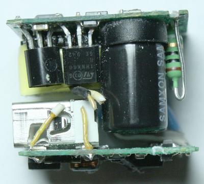
I assume the chip has these markings because it is being manufactured for Flextronics. The "EB936" marking on the chip could be Flextronics' own part number, or a date code.
.
I assume the chip has these markings because it is being manufactured for Flextronics. The "EB936" marking on the chip could be Flextronics' own part number, or a date code.
