What is the origin of the word "mainframe", referring to a large, complex computer? Most sources agree that the term is related to the frames that held early computers, but the details are vague.1 It turns out that the history is more interesting and complicated than you'd expect.
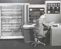
Based on my research, the earliest computer to use the term "main frame" was the IBM 701 computer (1952), which consisted of boxes called "frames." The 701 system consisted of two power frames, a power distribution frame, an electrostatic storage frame, a drum frame, tape frames, and most importantly a main frame. The IBM 701's main frame is shown in the documentation below.2

The meaning of "mainframe" has evolved, shifting from being a part of a computer to being a type of computer. For decades, "mainframe" referred to the physical box of the computer; unlike modern usage, this "mainframe" could be a minicomputer or even microcomputer. Simultaneously, "mainframe" was a synonym for "central processing unit." In the 1970s, the modern meaning started to develop—a large, powerful computer for transaction processing or business applications—but it took decades for this meaning to replace the earlier ones. In this article, I'll examine the history of these shifting meanings in detail.
Early computers and the origin of "main frame"
Early computers used a variety of mounting and packaging techniques including panels, cabinets, racks, and bays.3 This packaging made it very difficult to install or move a computer, often requiring cranes or the removal of walls.4 To avoid these problems, the designers of the IBM 701 computer came up with an innovative packaging technique. This computer was constructed as individual units that would pass through a standard doorway, would fit on a standard elevator, and could be transported with normal trucking or aircraft facilities.7 These units were built from a metal frame with covers attached, so each unit was called a frame. The frames were named according to their function, such as the power frames and the tape frame. Naturally, the main part of the computer was called the main frame.
, electrostatic storage unit/frame (with circular storage CRTs). Right: printer, card punch. Photo from BRL Report, thanks to Ed Thelen.")
The IBM 701's internal documentation used "main frame" frequently to indicate the main box of the computer, alongside "power frame", "core frame", and so forth. For instance, each component in the schematics was labeled with its location in the computer, "MF" for the main frame.6 Externally, however, IBM documentation described the parts of the 701 computer as units rather than frames.5
The term "main frame" was used by a few other computers in the 1950s.8 For instance, the JOHNNIAC Progress Report (August 8, 1952) mentions that "the main frame for the JOHNNIAC is ready to receive registers" and they could test the arithmetic unit "in the JOHNNIAC main frame in October."10 An article on the RAND Computer in 1953 stated that "The main frame is completed and partially wired" The main body of a computer called ERMA is labeled "main frame" in the 1955 Proceedings of the Eastern Computer Conference.9
 is on the right. Photo from NOAA.")
The progression of the word "main frame" can be seen in reports from the Ballistics Research Lab (BRL) that list almost all the computers in the United States. In the 1955 BRL report, most computers were built from cabinets or racks; the phrase "main frame" was only used with the IBM 650, 701, and 704. By 1961, the BRL report shows "main frame" appearing in descriptions of the IBM 702, 705, 709, and 650 RAMAC, as well as the Univac FILE 0, FILE I, RCA 501, READIX, and Teleregister Telefile. This shows that the use of "main frame" was increasing, but still mostly an IBM term.
The physical box of a minicomputer or microcomputer
In modern usage, mainframes are distinct from minicomputers or microcomputers. But until the 1980s, the word "mainframe" could also mean the main physical part of a minicomputer or microcomputer. For instance, a "minicomputer mainframe" was not a powerful minicomputer, but simply the main part of a minicomputer.13 For example, the PDP-11 is an iconic minicomputer, but DEC discussed its "mainframe."14. Similarly, the desktop-sized HP 2115A and Varian Data 620i computers also had mainframes.15 As late as 1981, the book Mini and Microcomputers mentioned "a minicomputer mainframe."

Even microcomputers had a mainframe: the cover of Radio Electronics (1978, above) stated, "Own your own Personal Computer: Mainframes for Hobbyists", using the definition below. An article "Introduction to Personal Computers" in Radio Electronics (Mar 1979) uses a similar meaning: "The first choice you will have to make is the mainframe or actual enclosure that the computer will sit in." The popular hobbyist magazine BYTE also used "mainframe" to describe a microprocessor's box in the 1970s and early 1980s16. BYTE sometimes used the word "mainframe" both to describe a large IBM computer and to describe a home computer box in the same issue, illustrating that the two distinct meanings coexisted.

Main frame synonymous with CPU
Words often change meaning through metonymy, where a word takes on the meaning of something closely associated with the original meaning. Through this process, "main frame" shifted from the physical frame (as a box) to the functional contents of the frame, specifically the central processing unit.17
The earliest instance that I could find of the "main frame" being equated with the central processing unit was in 1955. Survey of Data Processors stated: "The central processing unit is known by other names; the arithmetic and ligical [sic] unit, the main frame, the computer, etc. but we shall refer to it, usually, as the central processing unit." A similar definition appeared in Radio Electronics (June 1957, p37): "These arithmetic operations are performed in what is called the arithmetic unit of the machine, also sometimes referred to as the 'main frame.'"
The US Department of Agriculture's Glossary of ADP Terminology (1960) uses the definition: "MAIN FRAME - The central processor of the computer system. It contains the main memory, arithmetic unit and special register groups." I'll mention that "special register groups" is nonsense that was repeated for years.18 This definition was reused and extended in the government's Automatic Data Processing Glossary, published in 1962 "for use as an authoritative reference by all officials and employees of the executive branch of the Government" (below). This definition was reused in many other places, notably the Oxford English Dictionary.19
 the central processor of the computer system. It contains the main storage, arithmetic unit and special register groups. Synonymous with (CPU) and (central processing unit). (2) All that portion of a computer exclusive of the input, output, peripheral and in some instances, storage units.")
By the early 1980s, defining a mainframe as the CPU had become obsolete. IBM stated that "mainframe" was a deprecated term for "processing unit" in the Vocabulary for Data Processing, Telecommunications, and Office Systems (1981); the American National Dictionary for Information Processing Systems (1982) was similar. Computers and Business Information Processing (1983) bluntly stated: "According to the official definition, 'mainframe' and 'CPU' are synonyms. Nobody uses the word mainframe that way."
Mainframe vs. peripherals
Rather than defining the mainframe as the CPU, some dictionaries defined the mainframe in opposition to the "peripherals", the computer's I/O devices. The two definitions are essentially the same, but have a different focus.20 One example is the IFIP-ICC Vocabulary of Information Processing (1966) which defined "central processor" and "main frame" as "that part of an automatic data processing system which is not considered as peripheral equipment." Computer Dictionary (1982) had the definition "main frame—The fundamental portion of a computer, i.e. the portion that contains the CPU and control elements of a computer system, as contrasted with peripheral or remote devices usually of an input-output or memory nature."
One reason for this definition was that computer usage was billed for mainframe time, while other tasks such as printing results could save money by taking place directly on the peripherals without using the mainframe itself.21 A second reason was that the mainframe vs. peripheral split mirrored the composition of the computer industry, especially in the late 1960s and 1970s. Computer systems were built by a handful of companies, led by IBM. Compatible I/O devices and memory were built by many other companies that could sell them at a lower cost than IBM.22 Publications about the computer industry needed convenient terms to describe these two industry sectors, and they often used "mainframe manufacturers" and "peripheral manufacturers."
Main Frame or Mainframe?
An interesting linguistic shift is from "main frame" as two independent words to a compound word: either hyphenated "main-frame" or the single word "mainframe." This indicates the change from "main frame" being a type of frame to "mainframe" being a new concept. The earliest instance of hyphenated "main-frame" that I found was from 1959 in IBM Information Retrieval Systems Conference. "Mainframe" as a single, non-hyphenated word appears the same year in Datamation, mentioning the mainframe of the NEAC2201 computer. In 1962, the IBM 7090 Installation Instructions refer to a "Mainframe Diag[nostic] and Reliability Program." (Curiously, the document also uses "main frame" as two words in several places.) The 1962 book Information Retrieval Management discusses how much computer time document queries can take: "A run of 100 or more machine questions may require two to five minutes of mainframe time." This shows that by 1962, "main frame" had semantically shifted to a new word, "mainframe."
The rise of the minicomputer and how the "mainframe" become a class of computers
So far, I've shown how "mainframe" started as a physical frame in the computer, and then was generalized to describe the CPU. But how did "mainframe" change from being part of a computer to being a class of computers? This was a gradual process, largely happening in the mid-1970s as the rise of the minicomputer and microcomputer created a need for a word to describe large computers.
Although microcomputers, minicomputers, and mainframes are now viewed as distinct categories, this was not the case at first. For instance, a 1966 computer buyer's guide lumps together computers ranging from desk-sized to 70,000 square feet.23 Around 1968, however, the term "minicomputer" was created to describe small computers. The story is that the head of DEC in England created the term, inspired by the miniskirt and the Mini Minor car.24 While minicomputers had a specific name, larger computers did not.25
Gradually in the 1970s "mainframe" came to be a separate category, distinct from "minicomputer."2627 An early example is Datamation (1970), describing systems of various sizes: "mainframe, minicomputer, data logger, converters, readers and sorters, terminals." The influential business report EDP first split mainframes from minicomputers in 1972.28 The line between minicomputers and mainframes was controversial, with articles such as Distinction Helpful for Minis, Mainframes and Micro, Mini, or Mainframe? Confusion persists (1981) attempting to clarify the issue.29
With the development of the microprocessor, computers became categorized as mainframes, minicomputers or microcomputers. For instance, a 1975 Computerworld article discussed how the minicomputer competes against the microcomputer and mainframes. Adam Osborne's An Introduction to Microcomputers (1977) described computers as divided into mainframes, minicomputers, and microcomputers by price, power, and size. He pointed out the large overlap between categories and avoided specific definitions, stating that "A minicomputer is a minicomputer, and a mainframe is a mainframe, because that is what the manufacturer calls it."32
In the late 1980s, computer industry dictionaries started defining a mainframe as a large computer, often explicitly contrasted with a minicomputer or microcomputer. By 1990, they mentioned the networked aspects of mainframes.33
IBM embraces the mainframe label
Even though IBM is almost synonymous with "mainframe" now, IBM avoided marketing use of the word for many years, preferring terms such as "general-purpose computer."35 IBM's book Planning a Computer System (1962) repeatedly referred to "general-purpose computers" and "large-scale computers", but never used the word "mainframe."34 The announcement of the revolutionary System/360 (1964) didn't use the word "mainframe"; it was called a general-purpose computer system. The announcement of the System/370 (1970) discussed "medium- and large-scale systems." The System/32 introduction (1977) said, "System/32 is a general purpose computer..." The 1982 announcement of the 3084, IBM's most powerful computer at the time, called it a "large scale processor" not a mainframe.
IBM started using "mainframe" as a marketing term in the mid-1980s. For example, the 3270 PC Guide (1986) refers to "IBM mainframe computers." An IBM 9370 Information System brochure (c. 1986) says the system was "designed to provide mainframe power." IBM's brochure for the 3090 processor (1987) called them "advanced general-purpose computers" but also mentioned "mainframe computers." A System 390 brochure (c. 1990) discussed "entry into the mainframe class." The 1990 announcement of the ES/9000 called them "the most powerful mainframe systems the company has ever offered."

By 2000, IBM had enthusiastically adopted the mainframe label: the z900 announcement used the word "mainframe" six times, calling it the "reinvented mainframe." In 2003, IBM announced "The Mainframe Charter", describing IBM's "mainframe values" and "mainframe strategy." Now, IBM has retroactively applied the name "mainframe" to their large computers going back to 1959 (link), (link).
Mainframes and the general public
While "mainframe" was a relatively obscure computer term for many years, it became widespread in the 1980s. The Google Ngram graph below shows the popularity of "microcomputer", "minicomputer", and "mainframe" in books.36 The terms became popular during the late 1970s and 1980s. The popularity of "minicomputer" and "microcomputer" roughly mirrored the development of these classes of computers. Unexpectedly, even though mainframes were the earliest computers, the term "mainframe" peaked later than the other types of computers.

Dictionary definitions
I studied many old dictionaries to see when the word "mainframe" showed up and how they defined it. To summarize, "mainframe" started to appear in dictionaries in the late 1970s, first defining the mainframe in opposition to peripherals or as the CPU. In the 1980s, the definition gradually changed to the modern definition, with a mainframe distinguished as being large, fast, and often centralized system. These definitions were roughly a decade behind industry usage, which switched to the modern meaning in the 1970s.
The word didn't appear in older dictionaries, such as the Random House College Dictionary (1968) and Merriam-Webster (1974). The earliest definition I could find was in the supplement to Webster's International Dictionary (1976): "a computer and esp. the computer itself and its cabinet as distinguished from peripheral devices connected with it." Similar definitions appeared in Webster's New Collegiate Dictionary (1976, 1980).
A CPU-based definition appeared in Random House College Dictionary (1980): "the device within a computer which contains the central control and arithmetic units, responsible for the essential control and computational functions. Also called central processing unit." The Random House Dictionary (1978, 1988 printing) was similar. The American Heritage Dictionary (1982, 1985) combined the CPU and peripheral approaches: "mainframe. The central processing unit of a computer exclusive of peripheral and remote devices."
The modern definition as a large computer appeared alongside the old definition in Webster's Ninth New Collegiate Dictionary (1983): "mainframe (1964): a computer with its cabinet and internal circuits; also: a large fast computer that can handle multiple tasks concurrently." Only the modern definition appears in The New Merriram-Webster Dictionary (1989): "large fast computer", while Webster's Unabridged Dictionary of the English Language (1989): "mainframe. a large high-speed computer with greater storage capacity than a minicomputer, often serving as the central unit in a system of smaller computers. [MAIN + FRAME]." Random House Webster's College Dictionary (1991) and Random House College Dictionary (2001) had similar definitions.
The Oxford English Dictionary is the principal historical dictionary, so it is interesting to see its view. The 1989 OED gave historical definitions as well as defining mainframe as "any large or general-purpose computer, exp. one supporting numerous peripherals or subordinate computers." It has seven historical examples from 1964 to 1984; the earliest is the 1964 Honeywell Glossary. It quotes a 1970 Dictionary of Computers as saying that the word "Originally implied the main framework of a central processing unit on which the arithmetic unit and associated logic circuits were mounted, but now used colloquially to refer to the central processor itself." The OED also cited a Hewlett-Packard ad from 1974 that used the word "mainframe", but I consider this a mistake as the usage is completely different.15
Encyclopedias
A look at encyclopedias shows that the word "mainframe" started appearing in discussions of computers in the early 1980s, later than in dictionaries. At the beginning of the 1980s, many encyclopedias focused on large computers, without using the word "mainframe", for instance, The Concise Encyclopedia of the Sciences (1980) and World Book (1980). The word "mainframe" started to appear in supplements such as Britannica Book of the Year (1980) and World Book Year Book (1981), at the same time as they started discussing microcomputers. Soon encyclopedias were using the word "mainframe", for example, Funk & Wagnalls Encyclopedia (1983), Encyclopedia Americana (1983), and World Book (1984). By 1986, even the Doubleday Children's Almanac showed a "mainframe computer."
Newspapers
I examined old newspapers to track the usage of the word "mainframe." The graph below shows the usage of "mainframe" in newspapers. The curve shows a rise in popularity through the 1980s and a steep drop in the late 1990s. The newspaper graph roughly matches the book graph above, although newspapers show a much steeper drop in the late 1990s. Perhaps mainframes aren't in the news anymore, but people still write books about them.
.")
The first newspaper appearances were in classified ads seeking employees, for instance, a 1960 ad in the San Francisco Examiner for people "to monitor and control main-frame operations of electronic computers...and to operate peripheral equipment..." and a (sexist) 1966 ad in the Philadelphia Inquirer for "men with Digital Computer Bkgrnd [sic] (Peripheral or Mainframe)."37
By 1970, "mainframe" started to appear in news articles, for example, "The computer can't work without the mainframe unit." By 1971, the usage increased with phrases such as "mainframe central processor" and "'main-frame' computer manufacturers". 1972 had usages such as "the mainframe or central processing unit is the heart of any computer, and does all the calculations". A 1975 article explained "'Mainframe' is the industry's word for the computer itself, as opposed to associated items such as printers, which are referred to as 'peripherals.'" By 1980, minicomputers and microcomputers were appearing: "All hardware categories-mainframes, minicomputers, microcomputers, and terminals" and "The mainframe and the minis are interconnected."
By 1985, the mainframe was a type of computer, not just the CPU: "These days it's tough to even define 'mainframe'. One definition is that it has for its electronic brain a central processor unit (CPU) that can handle at least 32 bits of information at once. ... A better distinction is that mainframes have numerous processors so they can work on several jobs at once." Articles also discussed "the micro's challenge to the mainframe" and asked, "buy a mainframe, rather than a mini?"
By 1990, descriptions of mainframes became florid: "huge machines laboring away in glass-walled rooms", "the big burner which carries the whole computing load for an organization", "behemoth data crunchers", "the room-size machines that dominated computing until the 1980s", "the giant workhorses that form the nucleus of many data-processing centers", "But it is not raw central-processing-power that makes a mainframe a mainframe. Mainframe computers command their much higher prices because they have much more sophisticated input/output systems."
Conclusion
After extensive searches through archival documents, I found usages of the term "main frame" dating back to 1952, much earlier than previously reported. In particular, the introduction of frames to package the IBM 701 computer led to the use of the word "main frame" for that computer and later ones. The term went through various shades of meaning and remained fairly obscure for many years. In the mid-1970s, the term started describing a large computer, essentially its modern meaning. In the 1980s, the term escaped the computer industry and appeared in dictionaries, encyclopedias, and newspapers. After peaking in the 1990s, the term declined in usage (tracking the decline in mainframe computers), but the term and the mainframe computer both survive.
Two factors drove the popularity of the word "mainframe" in the 1980s with its current meaning of a large computer. First, the terms "microcomputer" and "minicomputer" led to linguistic pressure for a parallel term for large computers. For instance, the business press needed a word to describe IBM and other large computer manufacturers. While "server" is the modern term, "mainframe" easily filled the role back then and was nicely alliterative with "microcomputer" and "minicomputer."38
Second, up until the 1980s, the prototype meaning for "computer" was a large mainframe, typically IBM.39 But as millions of home computers were sold in the early 1980s, the prototypical "computer" shifted to smaller machines. This left a need for a term for large computers, and "mainframe" filled that need. In other words, if you were talking about a large computer in the 1970s, you could say "computer" and people would assume you meant a mainframe. But if you said "computer" in the 1980s, you needed to clarify if it was a large computer.
The word "mainframe" is almost 75 years old and both the computer and the word have gone through extensive changes in this time. The "death of the mainframe" has been proclaimed for well over 30 years but mainframes are still hanging on. Who knows what meaning "mainframe" will have in another 75 years?
Follow me on Bluesky (@righto.com) or RSS. (I'm no longer on Twitter.) Thanks to the Computer History Museum and archivist Sara Lott for access to many documents.
Notes and References
-
The Computer History Museum states: "Why are they called “Mainframes”? Nobody knows for sure. There was no mainframe “inventor” who coined the term. Probably “main frame” originally referred to the frames (designed for telephone switches) holding processor circuits and main memory, separate from racks or cabinets holding other components. Over time, main frame became mainframe and came to mean 'big computer.'" (Based on my research, I don't think telephone switches have any connection to computer mainframes.)
Several sources explain that the mainframe is named after the frame used to construct the computer. The Jargon File has a long discussion, stating that the term "originally referring to the cabinet containing the central processor unit or ‘main frame’." Ken Uston's Illustrated Guide to the IBM PC (1984) has the definition "MAIN FRAME A large, high-capacity computer, so named because the CPU of this kind of computer used to be mounted on a frame." IBM states that mainframe "Originally referred to the central processing unit of a large computer, which occupied the largest or central frame (rack)." The Microsoft Computer Dictionary (2002) states that the name mainframe "is derived from 'main frame', the cabinet originally used to house the processing unit of such computers." Some discussions of the origin of the word "mainframe" are here, here, here, here, and here.
The phrase "main frame" in non-computer contexts has a very old but irrelevant history, describing many things that have a frame. For example, it appears in thousands of patents from the 1800s, including drills, saws, a meat cutter, a cider mill, printing presses, and corn planters. This shows that it was natural to use the phrase "main frame" when describing something constructed from frames. Telephony uses a Main distribution frame or "main frame" for wiring, going back to 1902. Some people claim that the computer use of "mainframe" is related to the telephony use, but I don't think they are related. In particular, a telephone main distribution frame looks nothing like a computer mainframe. Moreover, the computer use and the telephony use developed separately; if the computer use started in, say, Bell Labs, a connection would be more plausible.
IBM patents with "main frame" include a scale (1922), a card sorter (1927), a card duplicator (1929), and a card-based accounting machine (1930). IBM's incidental uses of "main frame" are probably unrelated to modern usage, but they are a reminder that punch card data processing started decades before the modern computer. ↩
-
It is unclear why the IBM 701 installation manual is dated August 27, 1952 but the drawing is dated 1953. I assume the drawing was updated after the manual was originally produced. ↩
-
This footnote will survey the construction techniques of some early computers; the key point is that building a computer on frames was not an obvious technique. ENIAC (1945), the famous early vacuum tube computer, was constructed from 40 panels forming three walls filling a room (ref, ref). EDVAC (1949) was built from large cabinets or panels (ref) while ORDVAC and CLADIC (1949) were built on racks (ref). One of the first commercial computers, UNIVAC 1 (1951), had a "Central Computer" organized as bays, divided into three sections, with tube "chassis" plugged in (ref ). The Raytheon computer (1951) and Moore School Automatic Computer (1952) (ref) were built from racks. The MONROBOT VI (1955) was described as constructed from the "conventional rack-panel-cabinet form" (ref). ↩
-
The size and construction of early computers often made it difficult to install or move them. The early computer ENIAC required 9 months to move from Philadelphia to the Aberdeen Proving Ground. For this move, the wall of the Moore School in Philadelphia had to be partially demolished so ENIAC's main panels could be removed. In 1959, moving the SWAC computer required disassembly of the computer and removing one wall of the building (ref). When moving the early computer JOHNNIAC to a different site, the builders discovered the computer was too big for the elevator. They had to raise the computer up the elevator shaft without the elevator (ref). This illustrates the benefits of building a computer from moveable frames. ↩
-
The IBM 701's main frame was called the Electronic Analytical Control Unit in external documentation. ↩
-
The 701 installation manual (1952) has a frame arrangement diagram showing the dimensions of the various frames, along with a drawing of the main frame, and power usage of the various frames. Service documentation (1953) refers to "main frame adjustments" (page 74). The 700 Series Data Processing Systems Component Circuits document (1955-1959) lists various types of frames in its abbreviation list (below)
.") Abbreviations used in IBM drawings include MF for main frame. Also note CF for core frame, and DF for drum frame, From 700 Series Data Processing Systems Component Circuits (1955-1959).
Abbreviations used in IBM drawings include MF for main frame. Also note CF for core frame, and DF for drum frame, From 700 Series Data Processing Systems Component Circuits (1955-1959).When repairing an IBM 701, it was important to know which frame held which components, so "main frame" appeared throughout the engineering documents. For instance, in the schematics, each module was labeled with its location; "MF" stands for "main frame."
 in mainframe panel 3 (MF3) section J, column 29.
The blocks shown are an AND gate, OR gate, and Cathode Follower (buffer).
From System Drawings 1.04.1.") Detail of a 701 schematic diagram. "MF" stands for "main frame." This diagram shows part of a pluggable tube module (type 2891) in mainframe panel 3 (MF3) section J, column 29. The blocks shown are an AND gate, OR gate, and Cathode Follower (buffer). From System Drawings 1.04.1.
Detail of a 701 schematic diagram. "MF" stands for "main frame." This diagram shows part of a pluggable tube module (type 2891) in mainframe panel 3 (MF3) section J, column 29. The blocks shown are an AND gate, OR gate, and Cathode Follower (buffer). From System Drawings 1.04.1.The "main frame" terminology was used in discussions with customers. For example, notes from a meeting with IBM (April 8, 1952) mention "E. S. [Electrostatic] Memory 15 feet from main frame" and list "main frame" as one of the seven items obtained for the $15,000/month rental cost. ↩
-
For more information on how the IBM 701 was designed to fit on elevators and through doorways, see Building IBM: Shaping an Industry and Technology page 170, and The Interface: IBM and the Transformation of Corporate Design page 69. This is also mentioned in "Engineering Description of the IBM Type 701 Computer", Proceedings of the IRE Oct 1953, page 1285. ↩
-
Many early systems used "central computer" to describe the main part of the computer, perhaps more commonly than "main frame." An early example is the "central computer" of the Elecom 125 (1954). The Digital Computer Newsletter (Apr 1955) used "central computer" several times to describe the processor of SEAC. The 1961 BRL report shows "central computer" being used by Univac II, Univac 1107, Univac File 0, DYSEAC and RCA Series 300. The MIT TX-2 Technical Manual (1961) uses "central computer" very frequently. The NAREC glossary (1962) defined "central computer. That part of a computer housed in the main frame." ↩
-
This footnote lists some other early computers that used the term "main frame." The October 1956 Digital Computer Newsletter mentions the "main frame" of the IBM NORC. Digital Computer Newsletter (Jan 1959) discusses using a RAMAC disk drive to reduce "main frame processing time." This document also mentions the IBM 709 "main frame." The IBM 704 documentation (1958) says "Each DC voltage is distributed to the main frame..." (IBM 736 reference manual) and "Check the air filters in each main frame unit and replace when dirty." (704 Central Processing Unit).
The July 1962 Digital Computer Newsletter discusses the LEO III computer: "It has been built on the modular principle with the main frame, individual blocks of storage, and input and output channels all physically separate." The article also mentions that the new computer is more compact with "a reduction of two cabinets for housing the main frame."
The IBM 7040 (1964) and IBM 7090 (1962) were constructed from multiple frames, including the processing unit called the "main frame."11 Machines in IBM's System/360 line (1964) were built from frames; some models had a main frame, power frame, wall frame, and so forth, while other models simply numbered the frames sequentially.12 ↩
-
The 1952 JOHNNIAC progress report is quoted in The History of the JOHNNIAC. This memorandum was dated August 8, 1952, so it is the earliest citation that I found. The June 1953 memorandum also used the term, stating, "The main frame is complete." ↩
-
A detailed description of IBM's frame-based computer packaging is in Standard Module System Component Circuits pages 6-9. This describes the SMS-based packaging used in the IBM 709x computers, the IBM 1401, and related systems as of 1960. ↩
-
IBM System/360 computers could have many frames, so they were usually given sequential numbers. The Model 85, for instance, had 12 frames for the processor and four megabytes of memory in 18 frames (at over 1000 pounds each). Some of the frames had descriptive names, though. The Model 40 had a main frame (CPU main frame, CPU frame), a main storage logic frame, a power supply frame, and a wall frame. The Model 50 had a CPU frame, power frame, and main storage frame. The Model 75 had a main frame (consisting of multiple physical frames), storage frames, channel frames, central processing frames, and a maintenance console frame. The compact Model 30 consisted of a single frame, so the documentation refers to the "frame", not the "main frame." For more information on frames in the System/360, see 360 Physical Planning. The Architecture of the IBM System/360 paper refers to the "main-frame hardware." ↩
-
A few more examples that discuss the minicomputer's mainframe, its physical box: A 1970 article discusses the mainframe of a minicomputer (as opposed to the peripherals) and contrasts minicomputers with large scale computers. A 1971 article on minicomputers discusses "minicomputer mainframes." Computerworld (Jan 28, 1970, p59) discusses minicomputer purchases: "The actual mainframe is not the major cost of the system to the user." Modern Data (1973) mentions minicomputer mainframes several times. ↩
-
DEC documents refer to the PDP-11 minicomputer as a mainframe. The PDP-11 Conventions manual (1970) defined: "Processor: A unit of a computing system that includes the circuits controlling the interpretation and execution of instructions. The processor does not include the Unibus, core memory, interface, or peripheral devices. The term 'main frame' is sometimes used but this term refers to all components (processor, memory, power supply) in the basic mounting box." In 1976, DEC published the PDP-11 Mainframe Troubleshooting Guide. The PDP-11 mainframe is also mentioned in Computerworld (1977). ↩
-
Test equipment manufacturers started using the term "main frame" (and later "mainframe") around 1962, to describe an oscilloscope or other test equipment that would accept plug-in modules. I suspect this is related to the use of "mainframe" to describe a computer's box, but it could be independent. Hewlett-Packard even used the term to describe a solderless breadboard, the 5035 Logic Lab. The Oxford English Dictionary (1989) used HP's 1974 ad for the Logic Lab as its earliest citation of mainframe as a single word. It appears that the OED confused this use of "mainframe" with the computer use.
 Is this a mainframe? The HP 5035A Logic Lab was a power supply and support circuitry for a solderless breadboard. HP's ads referred to this as a "laboratory station mainframe."
 -
In the 1980s, the use of "mainframe" to describe the box holding a microcomputer started to conflict with "mainframe" as a large computer. For example, Radio Electronics (October 1982), started using the short-lived term "micro-mainframe" instead of "mainframe" for a microcomputer's enclosure. By 1985, Byte magazine had largely switched to the modern usage of "mainframe." But even as late as 1987, a review of the Apple IIGC described one of the system's components as the '"mainframe" (i.e. the actual system box)'. ↩
-
Definitions of "central processing unit" disagreed as to whether storage was part of the CPU, part of the main frame, or something separate. This was largely a consequence of the physical construction of early computers. Smaller computers had memory in the same frame as the processor, while larger computers often had separate storage frames for memory. Other computers had some memory with the processor and some external. Thus, the "main frame" might or might not contain memory, and this ambiguity carried over to definitions of CPU. (In modern usage, the CPU consists of the arithmetic/logic unit (ALU) and control circuitry, but excludes memory.) ↩
-
Many definitions of mainframe or CPU mention "special register groups", an obscure feature specific to the Honeywell 800 computer (1959). (Processors have registers, special registers are common, and some processors have register groups, but only the Honeywell 800 had "special register groups.") However, computer dictionaries kept using this phrase for decades, even though it doesn't make sense for other computers. I wrote a blog post about special register groups here. ↩
-
This footnote provides more examples of "mainframe" being defined as the CPU. The Data Processing Equipment Encyclopedia (1961) had a similar definition: "Main Frame: The main part of the computer, i.e. the arithmetic or logic unit; the central processing unit." The 1967 IBM 360 operator's guide defined: "The main frame - the central processing unit and main storage." The Department of the Navy's ADP Glossary (1970): "Central processing unit: A unit of a computer that includes the circuits controlling the interpretation and execution of instructions. Synonymous with main frame." This was a popular definition, originally from the ISO, used by IBM (1979) among others. Funk & Wagnalls Dictionary of Data Processing Terms (1970) defined: "main frame: The basic or essential portion of an assembly of hardware, in particular, the central processing unit of a computer." The American National Standard Vocabulary for Information Processing (1970) defined: "central processing unit: A unit of a computer that includes the circuits controlling the interpretation and execution of instructions. Synonymous with main frame." ↩
-
Both the mainframe vs. peripheral definition and the mainframe as CPU definition made it unclear exactly what components of the computer were included in the mainframe. It's clear that the arithmetic-logic unit and the processor control circuitry were included, while I/O devices were excluded, but some components such as memory were in a gray area. It's also unclear if the power supply and I/O interfaces (channels) are part of the mainframe. These distinctions were ignored in almost all of the uses of "mainframe" that I saw.
An unusual definition in a Goddard Space Center document (1965, below) partitioned equipment into the "main frame" (the electronic equipment), "peripheral equipment" (electromechanical components such as the printer and tape), and "middle ground equipment" (the I/O interfaces). The "middle ground" terminology here appears to be unique. Also note that computers are partitioned into "super speed", "large-scale", "medium-scale", and "small-scale."
") Definitions from Automatic Data Processing Equipment, Goddard Space Center, 1965. "Main frame" was defined as "The central processing unit of a system including the hi-speed core storage memory bank. (This is the electronic element.)
Definitions from Automatic Data Processing Equipment, Goddard Space Center, 1965. "Main frame" was defined as "The central processing unit of a system including the hi-speed core storage memory bank. (This is the electronic element.) -
This footnote gives some examples of using peripherals to save the cost of mainframe time. IBM 650 documentation (1956) describes how "Data written on tape by the 650 can be processed by the main frame of the 700 series systems." Univac II Marketing Material (1957) discusses various ways of reducing "main frame time" by, for instance, printing from tape off-line. The USAF Guide for auditing automatic data processing systems (1961) discusses how these "off line" operations make the most efficient use of "the more expensive main frame time." ↩
-
Peripheral manufacturers were companies that built tape drives, printers, and other devices that could be connected to a mainframe built by IBM or another company. The basis for the peripheral industry was antitrust action against IBM that led to the 1956 Consent Decree. Among other things, the consent decree forced IBM to provide reasonable patent licensing, which allowed other firms to build "plug-compatible" peripherals. The introduction of the System/360 in 1964 produced a large market for peripherals and IBM's large profit margins left plenty of room for other companies. ↩
-
Computers and Automation, March 1965, categorized computers into five classes, from "Teeny systems" (such as the IBM 360/20) renting for $2000/month, through Small, Medium, and Large systems, up to "Family or Economy Size Systems" (such as the IBM 360/92) renting for $75,000 per month. ↩
-
The term "minicomputer" was supposedly invented by John Leng, head of DEC's England operations. In the 1960s, he sent back a sales report: "Here is the latest minicomputer activity in the land of miniskirts as I drive around in my Mini Minor", which led to the term becoming popular at DEC. This story is described in The Ultimate Entrepreneur: The Story of Ken Olsen and Digital Equipment Corporation (1988). I'd trust the story more if I could find a reference that wasn't 20 years after the fact. ↩
-
For instance, Computers and Automation (1971) discussed the role of the minicomputer as compared to "larger computers." A 1975 minicomputer report compared minicomputers to their "general-purpose cousins." ↩
-
This footnote provides more on the split between minicomputers and mainframes. In 1971, Modern Data Products, Systems, Services contained .".. will offer mainframe, minicomputer, and peripheral manufacturers a design, manufacturing, and production facility...." Standard & Poor's Industry Surveys (1972) mentions "mainframes, minicomputers, and IBM-compatible peripherals." Computerworld (1975) refers to "mainframe and minicomputer systems manufacturers."
The 1974 textbook "Information Systems: Technology, Economics, Applications" couldn't decide if mainframes were a part of the computer or a type of computer separate from minicomputers, saying: "Computer mainframes include the CPU and main memory, and in some usages of the term, the controllers, channels, and secondary storage and I/O devices such as tape drives, disks, terminals, card readers, printers, and so forth. However, the equipment for storage and I/O are usually called peripheral devices. Computer mainframes are usually thought of as medium to large scale, rather than mini-computers."
Studying U.S. Industrial Outlook reports provides another perspective over time. U.S. Industrial Outlook 1969 divides computers into small, medium-size, and large-scale. Mainframe manufacturers are in opposition to peripheral manufacturers. The same mainframe vs. peripherals opposition appears in U.S. Industrial Outlook 1970 and U.S. Industrial Outlook 1971. The 1971 report also discusses minicomputer manufacturers entering the "maxicomputer market."30 1973 mentions "large computers, minicomputers, and peripherals." U.S. Industrial Outlook 1976 states, "The distinction between mainframe computers, minis, micros, and also accounting machines and calculators should merge into a spectrum." By 1977, the market was separated into "general purpose mainframe computers", "minicomputers and small business computers" and "microprocessors."
Family Computing Magazine (1984) had a "Dictionary of Computer Terms Made Simple." It explained that "A Digital computer is either a "mainframe", a "mini", or a "micro." Forty years ago, large mainframes were the only size that a computer could be. They are still the largest size, and can handle more than 100,000,000 instructions per second. PER SECOND! [...] Mainframes are also called general-purpose computers." ↩
-
In 1974, Congress held antitrust hearings into IBM. The thousand-page report provides a detailed snapshot of the meanings of "mainframe" at the time. For instance, a market analysis report from IDC illustrates the difficulty of defining mainframes and minicomputers in this era (p4952). The "Mainframe Manufacturers" section splits the market into "general-purpose computers" and "dedicated application computers" including "all the so-called minicomputers." Although this section discusses minicomputers, the emphasis is on the manufacturers of traditional mainframes. A second "Plug-Compatible Manufacturers" section discusses companies that manufactured only peripherals. But there's also a separate "Minicomputers" section that focuses on minicomputers (along with microcomputers "which are simply microprocessor-based minicomputers"). My interpretation of this report is the terminology is in the process of moving from "mainframe vs. peripheral" to "mainframe vs. minicomputer." The statement from Research Shareholders Management (p5416) on the other hand discusses IBM and the five other mainframe companies; they classify minicomputer manufacturers separately. (p5425) p5426 mentions "mainframes, small business computers, industrial minicomputers, terminals, communications equipment, and minicomputers." Economist Ralph Miller mentions the central processing unit "(the so-called 'mainframe')" (p5621) and then contrasts independent peripheral manufacturers with mainframe manufacturers (p5622). The Computer Industry Alliance refers to mainframes and peripherals in multiple places, and "shifting the location of a controller from peripheral to mainframe", as well as "the central processing unit (mainframe)" p5099. On page 5290, "IBM on trial: Monopoly tends to corrupt", from Harper's (May 1974), mentions peripherals compatible with "IBM mainframe units—or, as they are called, central processing computers." ↩
-
The influential business newsletter EDP provides an interesting view on the struggle to separate the minicomputer market from larger computers. Through 1968, they included minicomputers in the "general-purpose computer" category. But in 1969, they split "general-purpose computers" into "Group A, General Purpose Digital Computers" and "Group B, Dedicated Application Digital Computers." These categories roughly corresponded to larger computers and minicomputers, on the (dubious) assumption that minicomputers were used for a "dedicated application." The important thing to note is that in 1969 they did not use the term "mainframe" for the first category, even though with the modern definition it's the obvious term to use. At the time, EDP used "mainframe manufacturer" or "mainframer"31 to refer to companies that manufactured computers (including minicomputers), as opposed to manufacturers of peripherals. In 1972, EDP first mentioned mainframes and minicomputers as distinct types. In 1973, "microcomputer" was added to the categories. As the 1970s progressed, the separation between minicomputers and mainframes became common. However, the transition was not completely smooth; 1973 included a reference to "mainframe shipments (including minicomputers)."
To specific, the EDP Industry Report (Nov. 28, 1969) gave the following definitions of the two groups of computers:
Group A—General Purpose Digital Computers: These comprise the bulk of the computers that have been listed in the Census previously. They are character or byte oriented except in the case of the large-scale scientific machines, which have 36, 48, or 60-bit words. The predominant portion (60% to 80%) of these computers is rented, usually for $2,000 a month or more. Higher level languages such as Fortran, Cobol, or PL/1 are the primary means by which users program these computers.
Group B—Dedicated Application Digital Computers: This group of computers includes the "mini's" (purchase price below $25,000), the "midi's" ($25,000 to $50,000), and certain larger systems usually designed or used for one dedicated application such as process control, data acquisition, etc. The characteristics of this group are that the computers are usually word oriented (8, 12, 16, or 24-bits per word), the predominant number (70% to 100%) are purchased, and assembly language (at times Fortran) is the predominant means of programming. This type of computer is often sold to an original equipment manufacturer (OEM) for further system integration and resale to the final user.
These definitions strike me as rather arbitrary. ↩
-
In 1981 Computerworld had articles trying to clarify the distinctions between microcomputers, minicomputers, superminicomputers, and mainframes, as the systems started to overlay. One article, Distinction Helpful for Minis, Mainframes said that minicomputers were generally interactive, while mainframes made good batch machines and network hosts. Microcomputers had up to 512 KB of memory, minis were 16-bit machines with 512 KB to 4 MB of memory, costing up to $100,000. Superminis were 16- to 32-bit machines with 4 MB to 8 MB of memory, costing up to $200,000 but with less memory bandwidth than mainframes. Finally, mainframes were 32-bit machines with more than 8 MB of memory, costing over $200,000. Another article Micro, Mini, or Mainframe? Confusion persists described a microcomputer as using an 8-bit architecture and having fewer peripherals, while a minicomputer has a 16-bit architecture and 48 KB to 1 MB of memory. ↩
-
The miniskirt in the mid-1960s was shortly followed by the midiskirt and maxiskirt. These terms led to the parallel construction of the terms minicomputer, midicomputer, and maxicomputer.
The New York Times had a long article Maxi Computers Face Mini Conflict (April 5, 1970) explicitly making the parallel: "Mini vs. Maxi, the reigning issue in the glamorous world of fashion, is strangely enough also a major point of contention in the definitely unsexy realm of computers."
Although midicomputer and maxicomputer terminology didn't catch on the way minicomputer did, they still had significant use (example, midicomputer examples, maxicomputer examples).
The miniskirt/minicomputer parallel was done with varying degrees of sexism. One example is Electronic Design News (1969): "A minicomputer. Like the miniskirt, the small general-purpose computer presents the same basic commodity in a more appealing way." ↩
-
Linguistically, one indication that a new word has become integrated in the language is when it can be extended to form additional new words. One example is the formation of "mainframers", referring to companies that build mainframes. This word was moderately popular in the 1970s to 1990s. It was even used by the Department of Justice in their 1975 action against IBM where they described the companies in the systems market as the "mainframe companies" or "mainframers." The word is still used today, but usually refers to people with mainframe skills. Other linguistic extensions of "mainframe" include mainframing, unmainframe, mainframed, nonmainframe, and postmainframe. ↩
-
More examples of the split between microcomputers and mainframes: Softwide Magazine (1978) describes "BASIC versions for micro, mini and mainframe computers." MSC, a disk system manufacturer, had drives "used with many microcomputer, minicomputer, and mainframe processor types" (1980). ↩
-
Some examples of computer dictionaries referring to mainframes as a size category: Illustrated Dictionary of Microcomputer Terminology (1978) defines "mainframe" as "(1) The heart of a computer system, which includes the CPU and ALU. (2) A large computer, as opposed to a mini or micro." A Dictionary of Minicomputing and Microcomputing (1982) includes the definition of "mainframe" as "A high-speed computer that is larger, faster, and more expensive than the high-end minicomputers. The boundary between a small mainframe and a large mini is fuzzy indeed." The National Bureau of Standards Future Information Technology (1984) defined: "Mainframe is a term used to designate a medium and large scale CPU." The New American Computer Dictionary (1985) defined "mainframe" as "(1) Specifically, the rack(s) holding the central processing unit and the memory of a large computer. (2) More generally, any large computer. 'We have two mainframes and several minis.'" The 1990 ANSI Dictionary for Information Systems (ANSI X3.172-1990) defined: mainframe. A large computer, usually one to which other computers are connected in order to share its resources and computing power. Microsoft Press Computer Dictionary (1991) defined "mainframe computer" as "A high-level computer designed for the most intensive computational tasks. Mainframe computers are often shared by multiple users connected to the computer via terminals." ISO 2382 (1993) defines a mainframe as "a computer, usually in a computer center, with extensive capabilities and resources to which other computers may be connected so that they can share facilities."
The Microsoft Computer Dictionary (2002) had an amusingly critical definition of mainframe: "A type of large computer system (in the past often water-cooled), the primary data processing resource for many large businesses and organizations. Some mainframe operating systems and solutions are over 40 years old and have the capacity to store year values only as two digits." ↩
-
IBM's 1962 book Planning a Computer System (1962) describes how the Stretch computer's circuitry was assembled into frames, with the CPU consisting of 18 frames. The picture below shows how a "frame" was, in fact, constructed from a metal frame.
 could be rolled out of the frame (right)") In the Stretch computer, the circuitry (left) could be rolled out of the frame (right)
In the Stretch computer, the circuitry (left) could be rolled out of the frame (right) -
The term "general-purpose computer" is probably worthy of investigation since it was used in a variety of ways. It is one of those phrases that seems obvious until you think about it more closely. On the one hand, a computer such as the Apollo Guidance Computer can be considered general purpose because it runs a variety of programs, even though the computer was designed for one specific mission. On the other hand, minicomputers were often contrasted with "general-purpose computers" because customers would buy a minicomputer for a specific application, unlike a mainframe which would be used for a variety of applications. ↩
-
The n-gram graph is from the Google Books Ngram Viewer. The curves on the graph should be taken with a grain of salt. First, the usage of words in published books is likely to lag behind "real world" usage. Second, the number of usages in the data set is small, especially at the beginning. Nonetheless, the n-gram graph generally agrees with what I've seen looking at documents directly. ↩
-
More examples of "mainframe" in want ads: A 1966 ad from Western Union in The Arizona Republic looking for experience "in a systems engineering capacity dealing with both mainframe and peripherals." A 1968 ad in The Minneapolis Star for an engineer with knowledge of "mainframe and peripheral hardware." A 1968 ad from SDS in The Los Angeles Times for an engineer to design "circuits for computer mainframes and peripheral equipment." A 1968 ad in Fort Lauderdale News for "Computer mainframe and peripheral logic design." A 1972 ad in The Los Angeles Times saying "Mainframe or peripheral [experience] highly desired." In most of these ads, the mainframe was in contrast to the peripherals. ↩
-
A related factor is the development of remote connections from a microcomputer to a mainframe in the 1980s. This led to the need for a word to describe the remote computer, rather than saying "I connected my home computer to the other computer." See the many books and articles on connecting "micro to mainframe." ↩
-
To see how the prototypical meaning of "computer" changed in the 1980s, I examined the "Computer" article in encyclopedias from that time. The 1980 Concise Encyclopedia of the Sciences discusses a large system with punched-card input. In 1980, the World Book article focused on mainframe systems, starting with a photo of an IBM System/360 Model 40 mainframe. But in the 1981 supplement and the 1984 encyclopedia, the World Book article opened with a handheld computer game, a desktop computer, and a "large-scale computer." The article described microcomputers, minicomputers, and mainframes. Funk & Wagnalls Encyclopedia (1983) was in the middle of the transition; the article focused on large computers and had photos of IBM machines, but mentioned that future growth is expected in microcomputers. By 1994, the World Book article's main focus was the personal computer, although the mainframe still had a few paragraphs and a photo. This is evidence that the prototypical meaning of "computer" underwent a dramatic shift in the early 1980s from a mainframe to a balance between small and large computers, and then to the personal computer. ↩
.")
 in mainframe panel 3 (MF3) section J, column 29.
The blocks shown are an AND gate, OR gate, and Cathode Follower (buffer).
From System Drawings 1.04.1.")

")
 could be rolled out of the frame (right)")