Showing posts with label fpga. Show all posts

Reverse-engineering the first FPGA chip, the XC2064

A Field-Programmable Gate Array (FPGA) can implement arbitrary digital logic, anything from a microprocessor to a video generator or crypto miner. An FPGA consists of many logic blocks, each typically consisting of a flip flop and a logic function, along with a routing network that connects the logic blocks. What makes an FPGA special is that it is programmable hardware: you can redefine each logic block and the connections between them. The result is you can build a complex digital circuit without physically wiring up individual gates and flip flops or going to the expense of designing a custom integrated circuit.

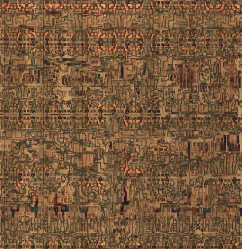
Die photo closeup showing the circuitry for one of the 64 tiles in the XC2064 FPGA. The metal layers have been removed, exposing the silicon and polysilicon transistors underneath. Click for a larger image. From siliconpr0n.

Die photo closeup showing the circuitry for one of the 64 tiles in the XC2064 FPGA. The metal layers have been removed, exposing the silicon and polysilicon transistors underneath. Click for a larger image. From siliconpr0n.

The FPGA was invented by Ross Freeman1 who co-founded Xilinx2 in 1984 and introduced the first FPGA, the XC2064. 3 This FPGA is much simpler than modern FPGAs—it contains just 64 logic blocks, compared to thousands or millions in modern FPGAs—but it led to the current multi-billion-dollar FPGA industry. Because of its importance, the XC2064 is in the Chip Hall of Fame. I reverse-engineered Xilinx's XC2064, and in this blog post I explain its internal circuitry (above) and how a "bitstream" programs it.

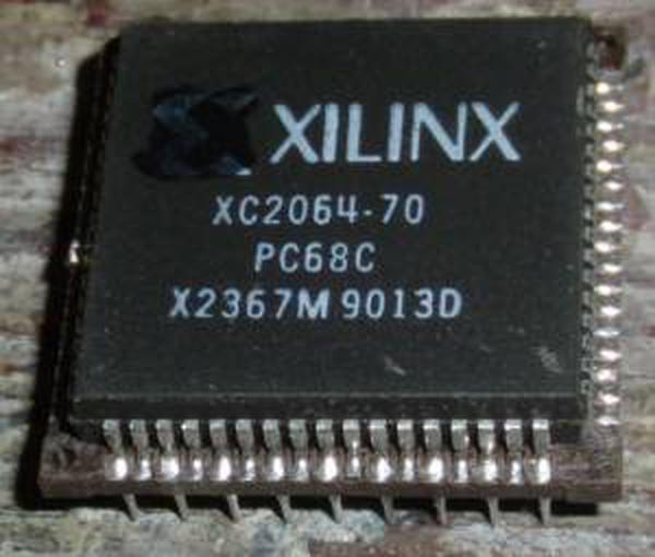
The Xilinx XC2064 was the first FPGA chip. Photo from siliconpr0n.

The Xilinx XC2064 was the first FPGA chip. Photo from siliconpr0n.

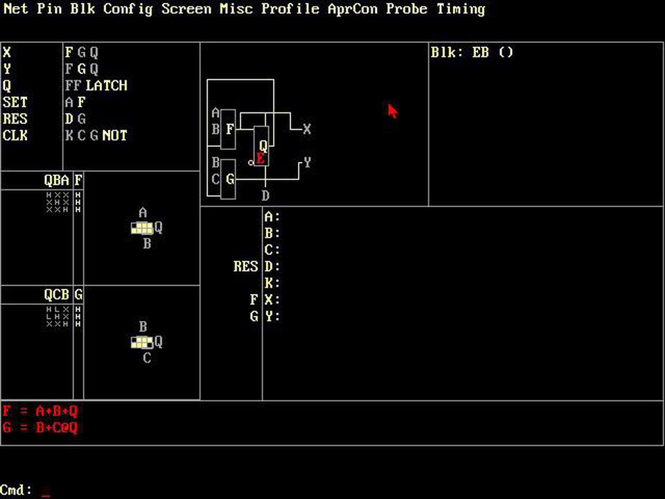
Nowadays, an FPGA is programed in a hardware description language such as Verilog or VHDL, but back then Xilinx provided their own development software, an MS-DOS application named XACT with a hefty $12,000 price tag. XACT operated at a lower level than modern tools: the user defined the function of each logic block, as shown in the screenshot below, and the connections between logic blocks. XACT routed the connections and generated a bitstream file that could be loaded into the FPGA.

Screenshot of XACT. The two lookup tables F and G implement the equations at the bottom of the screen, with Karnaugh map shown above.

Screenshot of XACT. The two lookup tables F and G implement the equations at the bottom of the screen, with Karnaugh map shown above.

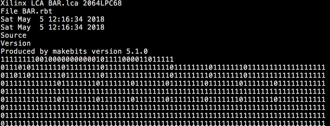
An FPGA is configured via the bitstream, a sequence of bits with a proprietary format. If you look at the bitstream for the XC2064 (below), it's a puzzling mixture of patterns that repeat irregularly with sequences scattered through the bitstream. There's no clear connection between the function definitions in XACT and the data in the bitstream. However, studying the physical circuitry of the FPGA reveals the structure of the bitstream data and it can be understood.

Part of the bitstream generated by XACT.

Part of the bitstream generated by XACT.

How does an FPGA work?

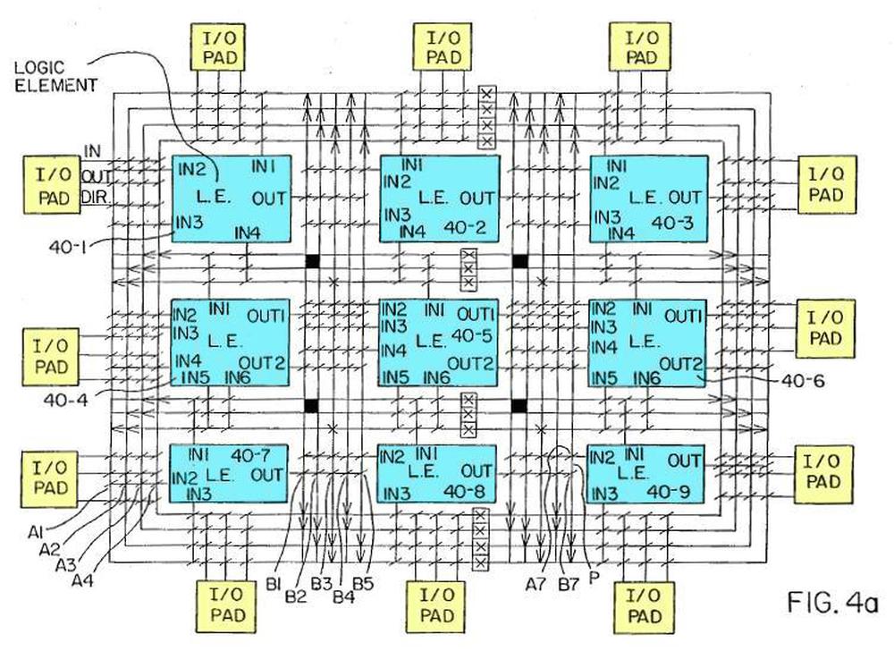
The diagram below, from the original FPGA patent, shows the basic structure of an FPGA. In this simplified FPGA, there are 9 logic blocks (blue) and 12 I/O pins. An interconnection network connects the components together. By setting switches (diagonal lines) on the interconnect, the logic blocks are connected to each other and to the I/O pins. Each logic element can be programmed with the desired logic function. The result is a highly programmable chip that can implement anything that fits in the available circuitry.

The FPGA patent shows logic blocks (LE) linked by an interconnect.

The FPGA patent shows logic blocks (LE) linked by an interconnect.

CLB: Configurable Logic Block

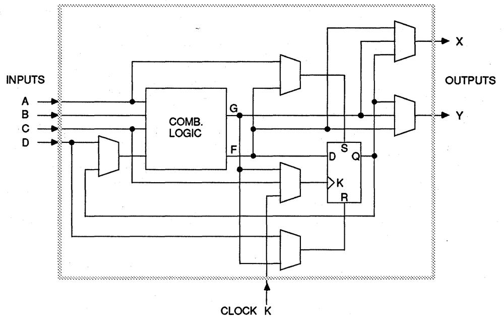
While the diagram above shows nine configurable logic blocks (CLBs), the XC2064 has 64 CLBs. The diagram below shows the structure of each CLB. Each CLB has four inputs (A, B, C, D) and two outputs (X and Y). In between is combinatorial logic, which can be programmed with any desired logic function. The CLB also contains a flip flop, allowing the FPGA to implement counters, shift registers, state machines and other stateful circuits. The trapezoids are multiplexers, which can be programmed to pass through any of their inputs. The multiplexers allow the CLB to be configured for a particular task, selecting the desired signals for the flip flop controls and the outputs.

A Configurable Logic Block in the XC2064, from the datasheet.

A Configurable Logic Block in the XC2064, from the datasheet.

You might wonder how the combinatorial logic implements arbitrary logic functions. Does it select between a collection of AND gates, OR gates, XOR gates, and so forth? No, it uses a clever trick called a lookup table (LUT), in effect holding the truth table for the function. For instance, a function of three variables is defined by the 8 rows in its truth table. The LUT consists of 8 bits of memory, along with a multiplexer circuit to select the right value. By storing values in these 8 bits of memory, any 3-input logic function can be implemented.4

The interconnect

The second key piece of the FPGA is the interconnect, which can be programmed to connect the CLBs in different ways. The interconnect is fairly complicated, but a rough description is that there are several horizontal and vertical line segments between each CLB. CLB. Interconnect points allow connections to be made between a horizontal line and a vertical line, allowing arbitrary paths to be created. More complex connections are done via "switch matrices". Each switch matrix has 8 pins, which can be wired together in (almost) arbitrary ways.

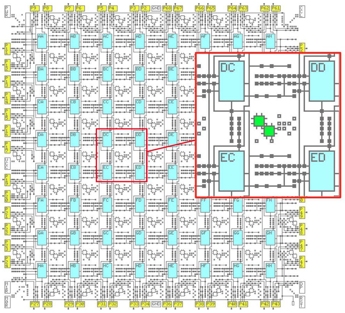
The diagram below shows the interconnect structure of the XC2064, providing connections to the logic blocks (cyan) and the I/O pins (yellow). The inset shows a closeup of the routing features. The green boxes are the 8-pin switch matrices, while the small squares are the programmable interconnection points.

The XC2064 FPGA has an 8 by 8 grid of CLBs. Each CLB has an alphabetic name from AA to HH.

The XC2064 FPGA has an 8 by 8 grid of CLBs. Each CLB has an alphabetic name from AA to HH.

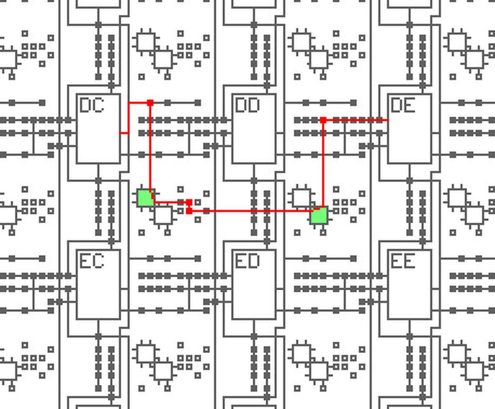
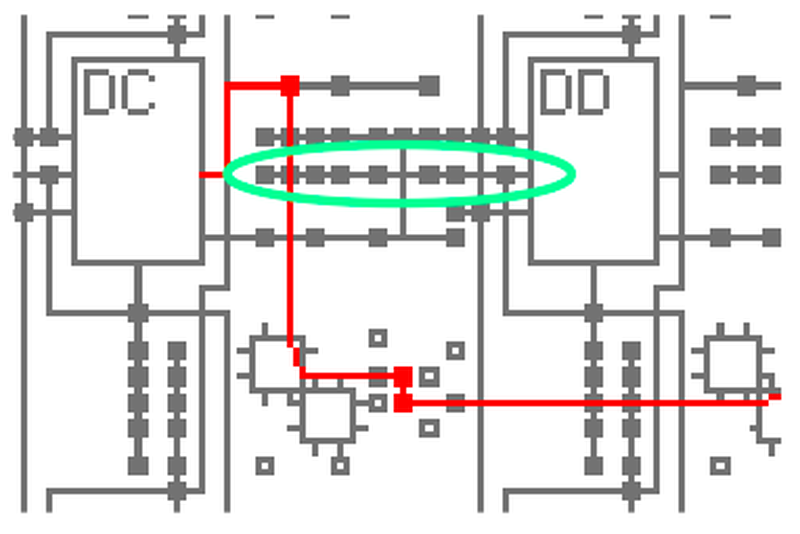
The interconnect can wire, for example, an output of block DC to an input of block DE, as shown below. The red line indicates the routing path and the small red squares indicate activated routing points. After leaving block DC, the signal is directed by the first routing point to an 8-pin switch (green) which directs it to two more routing points and another 8-pin switch. (The unused vertical and horizontal paths are not shown.) Note that routing is fairly complex; even this short path used four routing points and two switches.

Example of a signal routed from an output of block DC to block DE.

Example of a signal routed from an output of block DC to block DE.

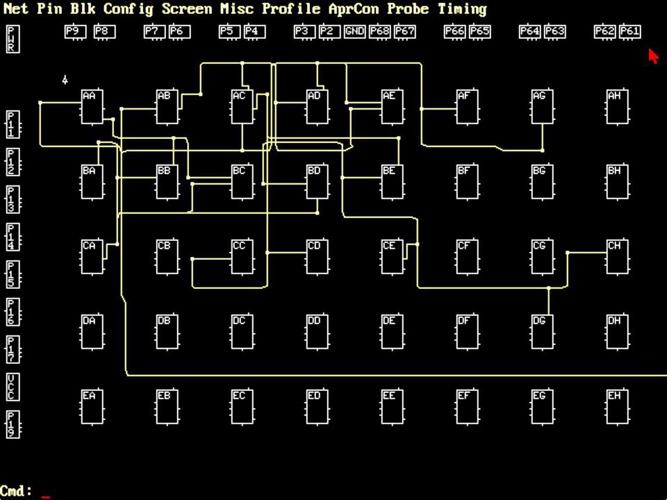
The screenshot below shows what routing looks like in the XACT program. The yellow lines indicate routing between the logic blocks. As more signals are added, the challenge is to route efficiently without the paths colliding. The XACT software package performs automatic routing, but routes can also be edited manually.

Screenshot of the XACT program.
This MS-DOS program was controlled via the keyboard and mouse.

Screenshot of the XACT program. This MS-DOS program was controlled via the keyboard and mouse.

The implementation

The remainder of this post discusses the internal circuitry of the XC2064, reverse-engineered from die photos.5 Be warned that this assumes some familiarity with the XC2064.

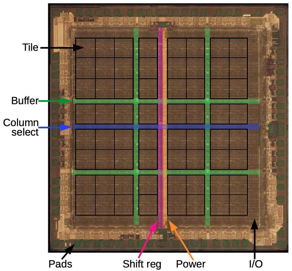
The die photo below shows the layout of the XC2064 chip. The main part of the FPGA is the 8×8 grid of tiles; each tile holds one logic block and the neighboring routing circuitry. Although FPGA diagrams show the logic blocks (CLBs) as separate entities from the routing that surrounds them, that is not how the FPGA is implemented. Instead, each logic block and the neighboring routing are implemented as a single entity, a tile. (Specifically, the tile includes the routing above and to the left of each CLB.)

Layout of the XC2064 chip. Image from siliconpr0n.

Layout of the XC2064 chip. Image from siliconpr0n.

Around the edges of the integrated circuit, I/O blocks provide communication with the outside world. They are connected to the small green square pads, which are wired to the chip's external pins. The die is divided by buffers (green): two vertical and two horizontal. These buffers amplify signals that travel long distances across the circuit, reducing delay. The vertical shift register (pink) and horizontal column select circuit (blue) are used to load the bitstream into the chip, as will be explained below.

Inside a tile

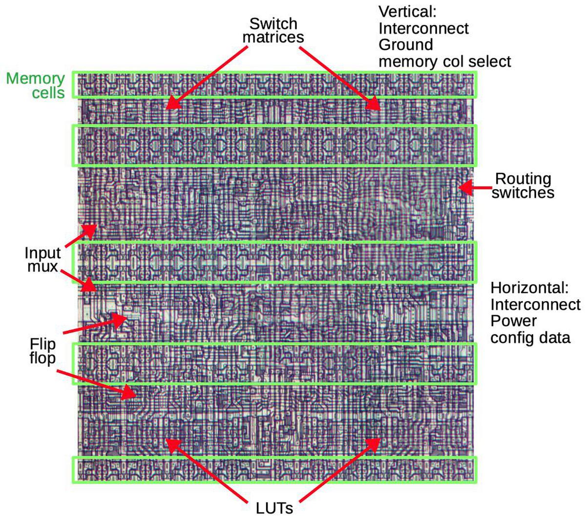
The diagram below shows the layout of a single tile in the XC2064; the chip contains 64 of these tiles packed together as shown above. About 40% of each tile is taken up by the memory cells (green) that hold the configuration bits. The top third (roughly) of the tile handles the interconnect routing through two switch matrices and numerous individual routing switches. Below that is the logic block. Key parts of the logic block are multiplexers for the input, the flip flop, and the lookup tables (LUTs). The tile is connected to neighboring tiles through vertical and horizontal wiring for interconnect, power and ground. The configuration data bits are fed into the memory cells horizontally, while vertical signals select a particular column of memory cells to load.

One tile of the FPGA, showing important functional units.

One tile of the FPGA, showing important functional units.

Transistors

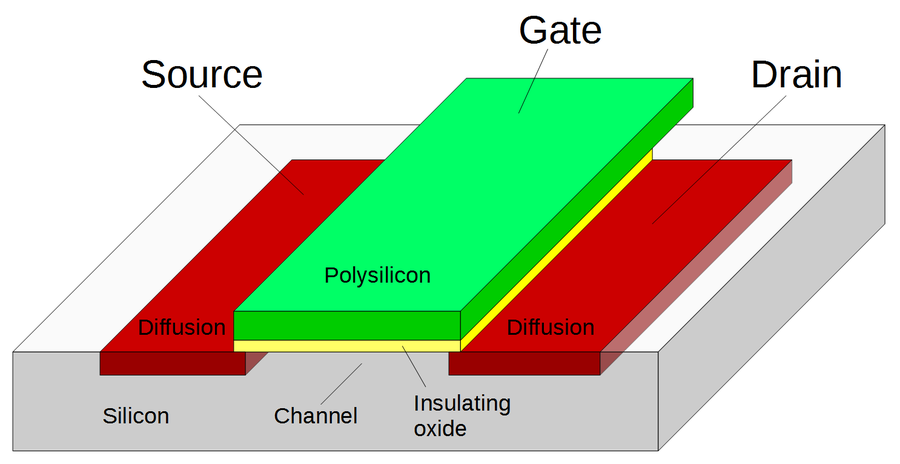
The FPGA is implemented with CMOS logic, built from NMOS and PMOS transistors. Transistors have two main roles in the FPGA. First, they can be combined to form logic gates. Second, transistors are used as switches that signals pass through, for instance to control routing. In this role, the transistor is called a pass transistor. The diagram below shows the basic structure of an MOS transistor. Two regions of silicon are doped with impurities to form the source and drain regions. In between, the gate turns the transistor on or off, controlling current flow between the source and drain. The gate is made of a special type of silicon called polysilicon, and is separated from the underlying silicon by a thin insulating oxide layer. Above this, two layers of metal provide wiring to connect the circuitry.

Structure of a MOSFET.

Structure of a MOSFET.

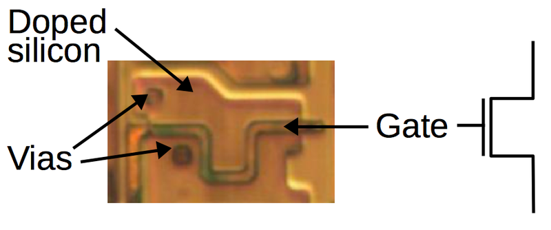
The die photo closeup below shows what a transistor looks like under a microscope. The polysilicon gate is the snaking line between the two doped silicon regions. The circles are vias, connections between the silicon and the metal layer (which has been removed for this photo).

A MOSFET as it appears in the FPGA.

A MOSFET as it appears in the FPGA.

The bitstream and configuration memory

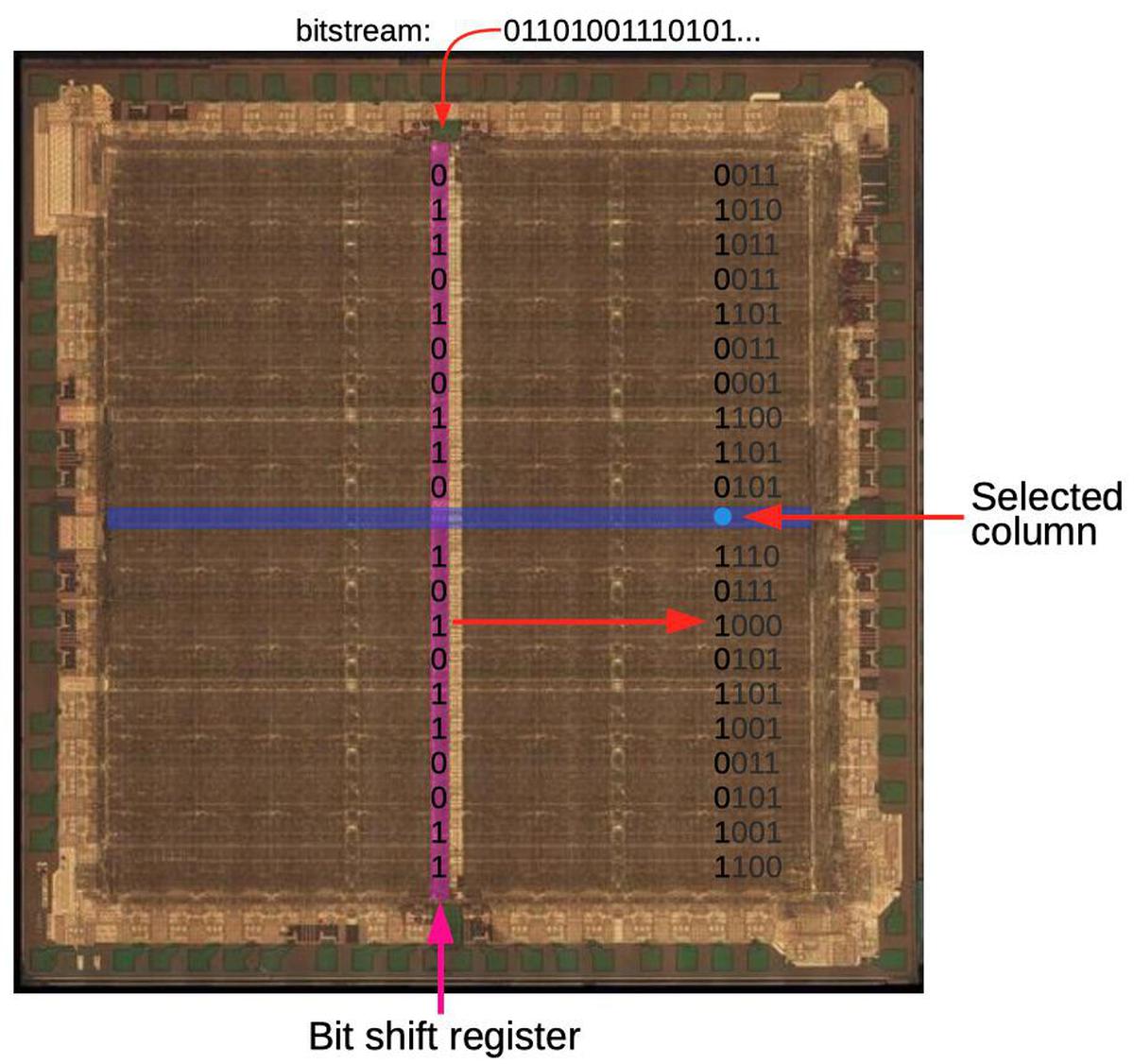
The configuration information in the XC2064 is stored in configuration memory cells. Instead of using a block of RAM for storage, the FPGA's memory is distributed across the chip in a 160×71 grid, ensuring that each bit is next to the circuitry that it controls. The diagram below shows how the configuration bitstream is loaded into the FPGA. The bitstream is fed into the shift register that runs down the center of the chip (pink). Once 71 bits have been loaded into the shift register, the column select circuit (blue) selects a particular column of memory and the bits are loaded into this column in parallel. Then, the next 71 bits are loaded into the shift register and the next column to the left becomes the selected column. This process repeats for all 160 columns of the FPGA, loading the entire bitstream into the chip. Using a shift register avoids bulky memory addressing circuitry.

How the bitstream is loaded into the FPGA. The bits shown are conceptual; actual bit storage is much denser. The three columns on the left have been loaded and the fourth column is currently being loaded. Die photo from siliconpr0n.

How the bitstream is loaded into the FPGA. The bits shown are conceptual; actual bit storage is much denser. The three columns on the left have been loaded and the fourth column is currently being loaded. Die photo from siliconpr0n.

The important point is that the bitstream is distributed across the chip exactly as it appears in the file: the layout of bits in the bitstream file matches the physical layout on the chip. As will be shown below, each bit is stored in the FPGA next to the circuit it controls. Thus, the bitstream file format is directly determined by the layout of the hardware circuits. For instance, when there is a gap between FPGA tiles because of the buffer circuitry, the same gap appears in the bitstream. The content of the bitstream is not designed around software concepts such as fields or data tables or configuration blocks. Understanding the bitstream depends on thinking of it in hardware terms, not in software terms.7

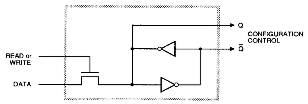
Each bit of configuration memory is implemented as shown below.8 Each memory cell consists of two inverters connected in a loop. This circuit has two stable states so it can store a bit: either the top inverter is 1 and the bottom is 0 or vice versa. To write to the cell, the pass transistor on the left is activated, passing the data signal through. The signal on the data line simply overpowers the inverters, writing the desired bit. (You can also read the configuration data out of the FPGA using the same path.) The Q and inverted Q outputs control the desired function in the FPGA, such as closing a routing connection, providing a bit for a lookup table, or controlling the flip flops. (In most cases, just the Q output is used.)

Schematic diagram of one bit of configuration memory, from the datasheet. Q is the output and Q is the inverted output.

Schematic diagram of one bit of configuration memory, from the datasheet. Q is the output and Q is the inverted output.

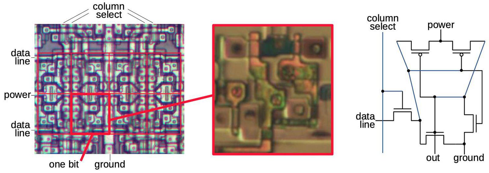
The diagram below shows the physical layout of memory cells. The photo on the left shows eight memory cells, with one cell highlighted. Each horizontal data line feeds all the memory cells in that row. Each column select line selects all the memory cells in that column for writing. The middle photo zooms in on the silicon and polysilicon transistors for one memory cell. The metal layers were removed to expose the underlying transistors. The metal layers wire together the transistors; the circles are connections (vias) between the silicon or polysilicon and the metal. The schematic shows how the five transistors are connected; the schematic's physical layout matches the photo. Two pairs of transistors form two CMOS inverters, while the pass transistor in the lower left provides access to the cell.

Eight bits of configuration memory, four above and four below. The red box shows one bit. When a column select line is activated, the row data line is loaded into the corresponding cells. The closeup and schematic show one bit of configuration memory. Die photo from siliconpr0n.

Eight bits of configuration memory, four above and four below. The red box shows one bit. When a column select line is activated, the row data line is loaded into the corresponding cells. The closeup and schematic show one bit of configuration memory. Die photo from siliconpr0n.

Lookup table multiplexers

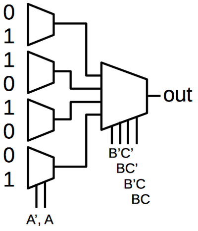
As explained earlier, the FPGA implements arbitrary logic functions by using a lookup table. The diagram below shows how a lookup table is implemented in the XC2064. The eight values on the left are stored in eight memory cells. Four multiplexers select one of each pair of values, depending on the value of the A input; if A is 0, the top value is selected and if A is 1 the bottom value is selected. Next, a larger multiplexer selects one of the four values based on B and C. The result is the desired value, in this case A XOR B XOR C. By putting different values in the lookup table, the logic function can be changed as desired.

Implementing XOR with a lookup table.

Implementing XOR with a lookup table.

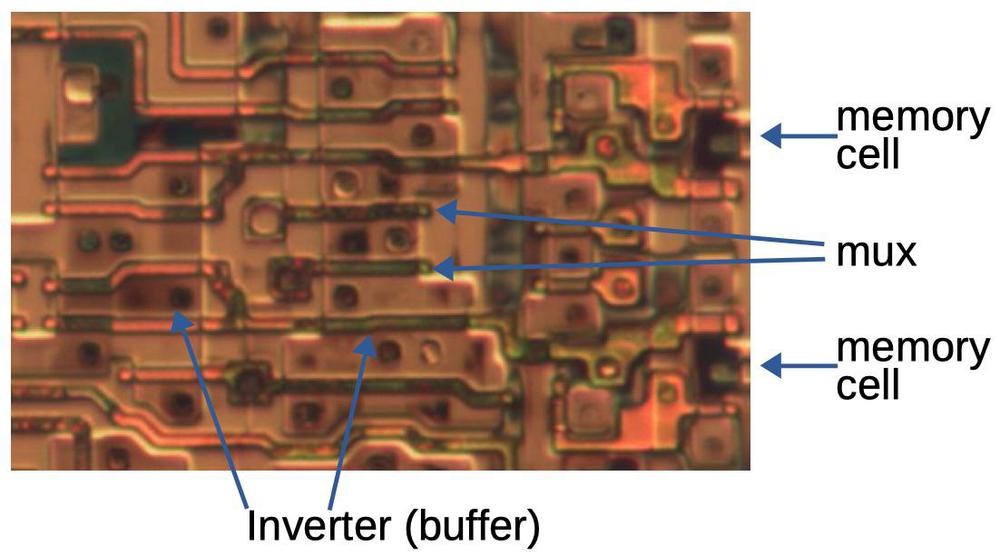
Each multiplexer is implemented with pass transistors. Depending on the control signals, one of the pass transistors is activated, passing that input to the output. The diagram below shows part of the LUT circuitry, multiplexing two of the bits. At the right are two of the memory cells. Each bit goes through an inverter to amplify it, and then passes through the multiplexer's pass transistors in the middle, selecting one of the bits.

A closeup of circuitry in the LUT implementation. Die photo from siliconpr0n.

A closeup of circuitry in the LUT implementation. Die photo from siliconpr0n.

Flip flop

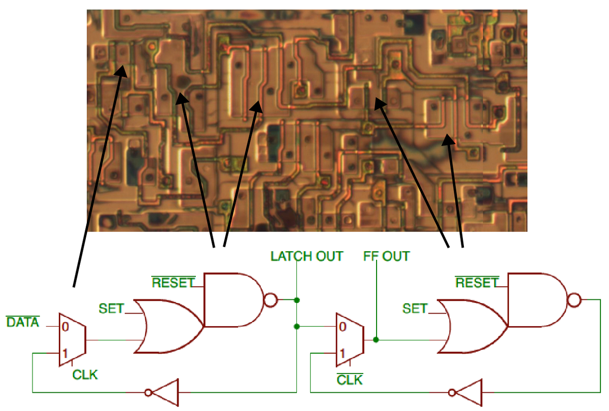
Each CLB contains a flip flop, allowing the FPGA to implement latches, state machines, and other stateful circuits. The diagram below shows the (slightly unusual) implementation of the flip flop. It uses a primary/secondary design. When the clock is low, the first multiplexer lets the data into the primary latch. When the clock goes high, the multiplexer closes the loop for the first latch, holding the value. (The bit is inverted twice going through the OR gate, NAND gate, and inverter, so it is held constant.) Meanwhile, the secondary latch's multiplexer receives the bit from the first latch when the clock goes high (note that the clock is inverted). This value becomes the flip flop's output. When the clock goes low, the secondary's multiplexer closes the loop, latching the bit. Thus, the flip flop is edge-sensitive, latching the value on the rising edge of the clock. The set and reset lines force the flip flop high or low.

Flip flop implementation. The arrows point out the first multiplexer and the two OR-NAND gates. Die photo from siliconpr0n.

Flip flop implementation. The arrows point out the first multiplexer and the two OR-NAND gates. Die photo from siliconpr0n.

8-pin switch matrix

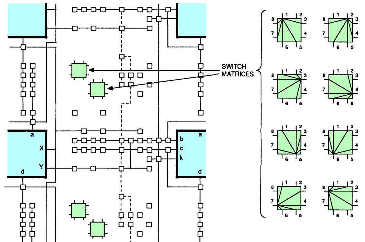
The switch matrix is an important routing element. Each switch has eight "pins" (two on each side) and can connect almost any combination of pins together. This allows signals to turn, split, or cross over with more flexibility than the individual routing nodes. The diagram below shows part of the routing network between four CLBs (cyan). The switch matrices (green) can be connected with any combination of the connections on the right. Note that each pin can connect to 5 of the 7 other pins. For instance, pin 1 can connect to pin 3 but not pin 2 or 4. This makes the matrix almost a crossbar, with 20 potential connections rather than 28.

Based on Xilinx Programmable Gate Array Data Book, fig 7b.

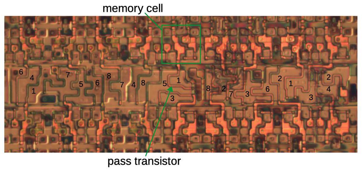
The switch matrix is implemented by a row of pass transistors controlled by memory cells above and below. The two sides of the transistor are the two switch matrix pins that can be connected by that transistor. Thus, each switch matrix has 20 associated control bits;9 two matrices per tile yields matrix 40 control bits per tile. The photo below indicates one of the memory cells, connected to the long squiggly gate of the pass transistor below. This transistor controls the connection between pin 5 and pin 1. Thus, the bit in the bitstream corresponding to that memory cell controls the switch connection between pin 5 and pin 1. Likewise, the other memory cells and their associated transistors control other switch connections. Note that the ordering of these connections follows no particular pattern; consequently, the mapping between bitstream bits and the switch pins appears random.

Implementation of an 8-pin switch matrix. The silicon regions are labeled with the corresponding pin numbers.
The metal layers (which connect the pins to the transistors) were removed for this photo.
Based on die photo from siliconpr0n.

Implementation of an 8-pin switch matrix. The silicon regions are labeled with the corresponding pin numbers. The metal layers (which connect the pins to the transistors) were removed for this photo. Based on die photo from siliconpr0n.

Input routing

The inputs to a CLB use a different encoding scheme in the bitstream, which is explained by the hardware implementation. In the diagram below, the eight circled nodes are potential inputs to CLB box DD. Only one node (at most) can be configured as an input, since connecting two signals to the same input would short them together.

Input selection. The eight nodes circled in green are potential inputs to DD; one of them can be selected.

Input selection. The eight nodes circled in green are potential inputs to DD; one of them can be selected.

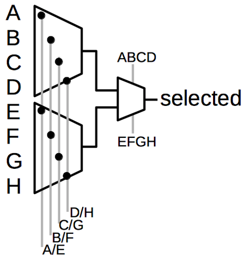
The desired input is selected using a multiplexer. A straightforward solution would use an 8-way multiplexer, with 3 control bits selecting one of the 8 signals. Another straightforward solution would be to use 8 pass transistors, each with its own control signal, with one of them selecting the desired signal. However, the FPGA uses a hybrid approach that avoids the decoding hardware of the first approach but uses 5 control signals instead of the eight required by the second approach.

The FPGA uses multiplexers to select one of eight inputs.

The FPGA uses multiplexers to select one of eight inputs.

The schematic above shows the two-stage multiplexer approach used in the FPGA. In the first stage, one of the control signals is activated. The second stage picks either the top or bottom signal for the output.10 For instance, suppose control signal B/F is sent to the first stage and 'ABCD' to the second stage; input B is the only one that will pass through to the output. Thus, selecting one of the eight inputs requires 5 bits in the bitstream and uses 5 memory cells.

Conclusion

The XC2064 uses a variety of highly-optimized circuits to implement its logic blocks and routing. This circuitry required a tight layout in order to fit onto the die. Even so, the XC2064 was a very large chip, larger than microprocessors of the time, so it was difficult to manufacture at first and cost hundreds of dollars. Compared to modern FPGAs, the XC2064 had an absurdly small number of cells, but even so it sparked a revolutionary new product line.

Two concepts are the key to understanding the XC2064's bitstream. First, the FPGA is implemented from 64 tiles, repeated blocks that combine the logic block and routing. Although FPGAs are described as having logic blocks surrounded by routing, that is not how they are implemented. The second concept is that there are no abstractions in the bitstream; it is mapped directly onto the two-dimensional layout of the FPGA. Thus, the bitstream only makes sense if you consider the physical layout of the FPGA.

I've determined how most of the XC2064 bitstream is configured (see footnote 11) and I've made a program to generate the CLB information from a bitstream file. Unfortunately, this is one of those projects where the last 20% takes most of the time, so there's still work to be done. One problem is handling I/O pins, which are full of irregularities and their own routing configuration. Another problem is the tiles around the edges have slightly different configurations. Combining the individual routing points into an overall netlist also requires some tedious graph calculations.

I announce my latest blog posts on Twitter, so follow me at kenshirriff for updates. I also have an RSS feed. Thanks to John McMaster, Tim Ansell and Philip Freidin for discussions.12

Notes and references

  1. Ross Freeman tragically died of pneumonia at age 45, five years after inventing the FPGA. In 2009, Freeman was recognized as the inventor of the FPGA by the Inventor's Hall of Fame

  2. Xilinx was one of the first fabless semiconductor companies. Unlike most semiconductor companies that designed and manufactured semiconductors, Xilinx only created the design while a fab company did the manufacturing. Xilinx used Seiko Epson Semiconductor Division (as in Seiko watches and Epson printers) for their initial fab. 

  3. Custom integrated circuits have the problems of high cost and the long time (months or years) to design and manufacture the chip. One solution was Programmable Logic Devices (PLD), chips with gate arrays that can be programmed with various functions, which were developed around 1967. Originally they were mask-programmable; the metal layer of the chip was designed for the desired functionality, a new mask was made, and chips were manufactured to the specifications. Later chips contained a PROM that could be "field programmed" by blowing tiny fuses inside the chip to program it, or an EPROM that could be reprogrammed. Programmable logic devices had a variety of marketing names including Programmable Logic Array, Programmable Array Logic (1978), Generic Array Logic and Uncommitted Logic Array. For the most part, these devices consisted of logic gates arranged as a sum-of-products, although some included flip flops. The main innovation of the FPGA was to provide a programmable interconnect between logic blocks, rather than a fixed gate architecture, as well as logic blocks with flip flops. For an in-depth look at FPGA history and the effects of scalability, see Three Ages of FPGAs: A Retrospective on the First Thirty Years of FPGA Technology. Also see A Brief History of FPGAs

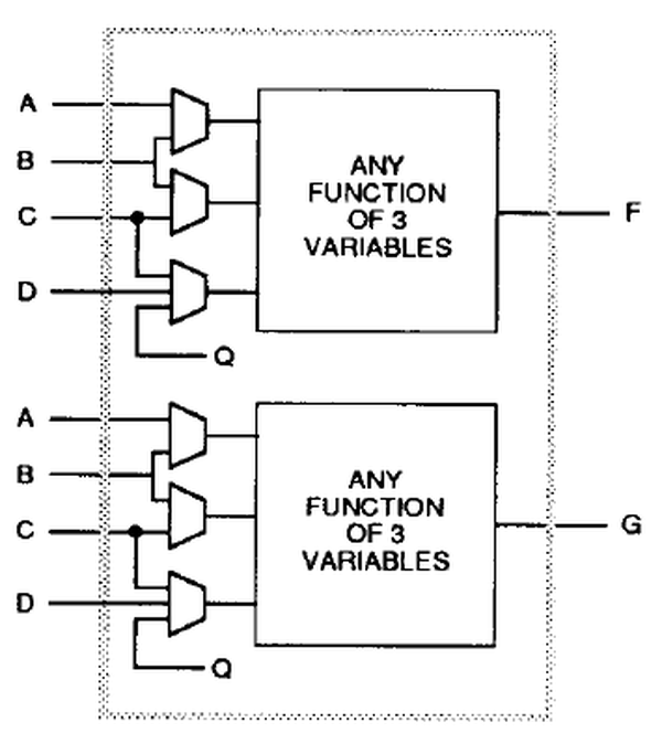
  4. The lookup tables in the XC2064 are more complex than just a table. Each CLB contains two 3-input lookup tables. The inputs to the lookup tables in the XC2064 have programmable multiplexers, allowing selection of four different potential inputs. In addition, the two lookup tables can be tied together to create a function on four variables or other combinations.

    Logic functions in the XC2064 FPGA are implemented with lookup tables. From the datasheet.

    Logic functions in the XC2064 FPGA are implemented with lookup tables. From the datasheet.


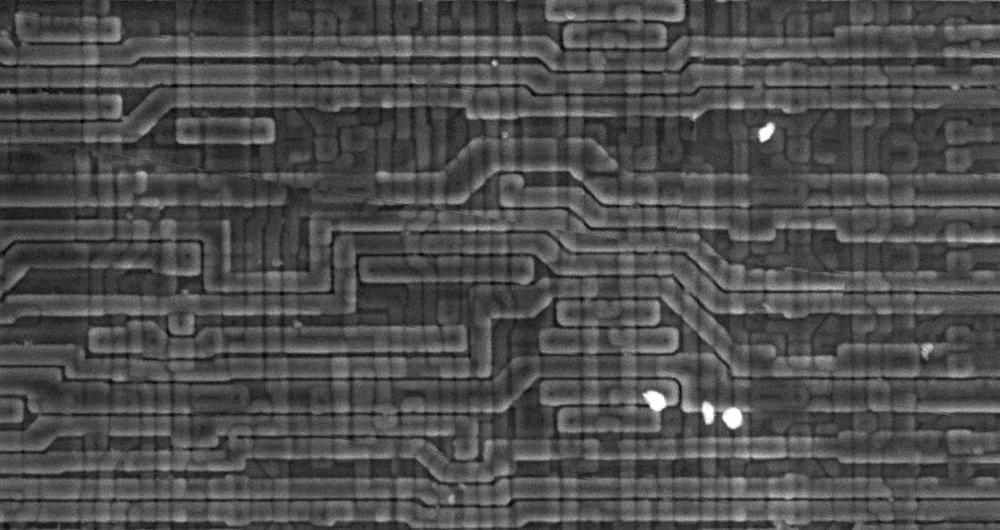
  5. To analyze the XC2064, I used my own die photos of the XC20186 as well as the siliconpr0n photos of the XC2064 and XC2018. Under a light microscope, the FPGA is hard to analyze because it has two metal layers. John McMaster used his electron microscope to help disambiguate the two layers. The photo below shows how the top metal layer is emphasized by the electron microscope.

    Electron microscope photo of the XC2064, courtesy of John McMaster.

    Electron microscope photo of the XC2064, courtesy of John McMaster.


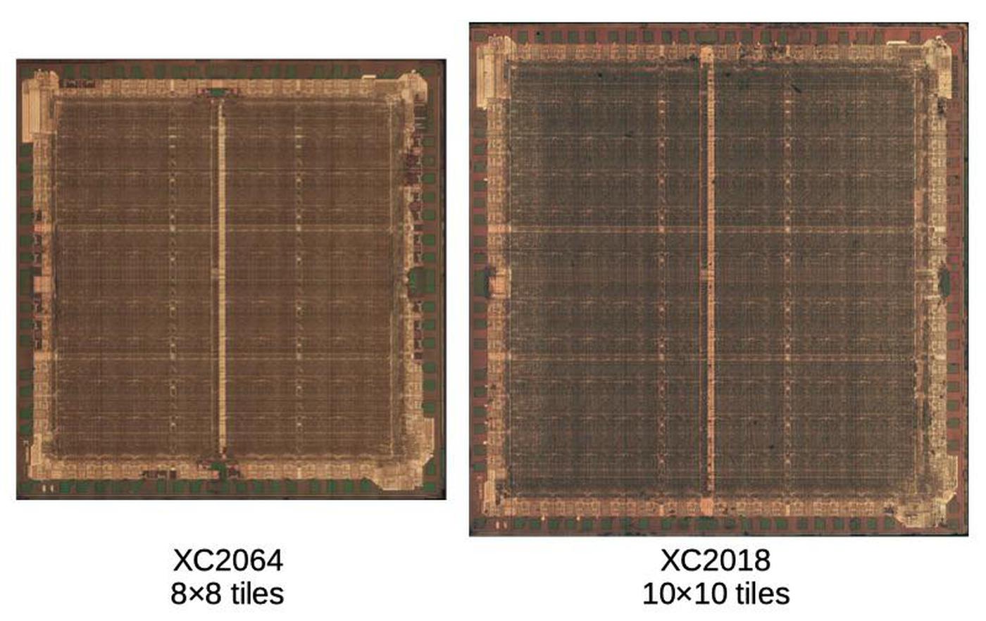
  6. The Xilinx XC2018 FPGA (below) is a 100-cell version of the XC2064 FPGA. Internally, it uses the same tiles as the 64-cell XC2064, except it has a 10×10 grid of tiles instead of an 8×8 grid. The bitstream format of the XC2018 is very similar, except with more entries.

    The Xilinx XC2018 FPGA. On the right, the lid has been removed, showing the silicon die. The tile pattern is faintly visible on the die.

    The Xilinx XC2018 FPGA. On the right, the lid has been removed, showing the silicon die. The tile pattern is faintly visible on the die.

    The image below compares the XC2064 die with the XC2018 die. The dies are very similar, except the larger chip has two more rows and columns of tiles.

    Comparison of the XC2064 and XC2018 dies. The images are scaled so the tile sizes match; I don't know how the physical sizes of the dies compare. Die photos from siliconpr0n.

    Comparison of the XC2064 and XC2018 dies. The images are scaled so the tile sizes match; I don't know how the physical sizes of the dies compare. Die photos from siliconpr0n.


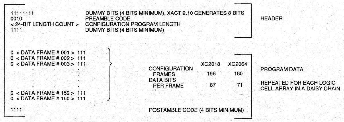
  7. While the bitstream directly maps onto the hardware layout, the bitstream file (.RBT) does have a small amount of formatting, shown below.

    The format of the bitstream data, from the datasheet.

    The format of the bitstream data, from the datasheet.


  8. The configuration memory is implemented as static RAM (SRAM) cells. (Technically, the memory is not RAM since it must be accessed sequentially through the shift register, but people still call it SRAM.) These memory cells have five transistors, so they are known as 5T SRAM.

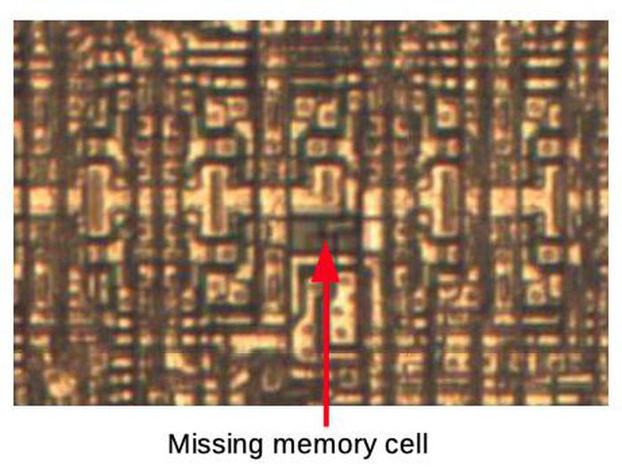
    One question that comes up is if there are any unused bits in the bitstream. It turns out that many bits are unused. For instance, each tile has an 18×8 block of bits assigned to it, of which 27 bits are unused. Looking at the die shows that the memory cell for an unused bit is omitted entirely, allowing that die area to be used for other circuitry. The die photo below shows 9 implemented bits and one missing bit.

    Memory cells, showing a gap where one cell is missing. Die photo from siliconpr0n.

    Memory cells, showing a gap where one cell is missing. Die photo from siliconpr0n.


  9. The switch matrix has 20 pass transistors. Since each tile is 18 memory cells wide, two of the transistors are connected to slightly more distant memory cells. 

  10. A few notes on the CLB input multiplexer. The control signal EFGH is the complement of ABCD, so only one control signal is needed in the bitstream and only one memory cell for this signal. Second, other inputs to the CLB have 6 or 10 choices; the same two-level multiplexer approach is used, changing the number of inputs and control signals. Finally, a few of the control signals are inverted (probably because the inverted memory output was closer). This can cause confusion when trying to understand the bitstream, since some bits appear to select 6 inputs instead of 2. Looking at the complemented bit, instead, restores the pattern. 

  11. The following table summarizes the meaning of each bit in a tile's 8×18 part of the bitstream. Each entry in the table corresponds to one bit in the bitstream and indicates what part of the FPGA is controlled by that bit. Empty entries indicate unused bits.

    #2: 1-3#2: 3-4PIP D2,D5 (bit inverted)Gin_3 = DG = 1 2' 3'
    #2: 1-2#2: 2-6#2: 2-4PIP A2,A5 (bit inverted)Gin_3 = CG = 1' 2' 3'
    #2: 3-7#2: 3-6PIP D3, D4, D5PIP A3, A4, A5G = 1' 2 3'
    #2: 2-7#2: 2-8ND 11PIP A1, A4G = 1 2 3'
    #2: 1-5#2: 3-5PIP A3, AXPIP D1, D4Y=FG = 1 2' 3
    #2: 4-8#2: 5-8ND 10PIP D3, DXY=GGin_2 = BG = 1' 2' 3
    #2: 7-8#2: 6-8ND 9PIP B2, B5, B6, BX, BYPIP Y2X=GGin_1 = AG = 1' 2 3
    #2: 5-6#2: 5-7ND 8PIP B3,BX (bit inverted)PIP Y4X=FG = 1 2 3
    #2: 4-6#2: 1-4#2: 1-7PIP C1, C3, C4, C7PIP X3Q = LATCHBase FG (separate LUTs)
    #1: 3-5#1: 5-8#1: 2-8PIP X2
    #1: 3-4#1: 2-4ND 7PIP C3,CX (bit inverted)PIP X1Fin_1 = AF = ! 1 2 3
    #1: 1-2#1: 1-3ND 6PIP B6, B7CLK = enabledFin_2 = BF = 1' 2 3
    #1: 1-5#1: 1-4ND 5PIP C6, C7CLK = inverted (FF), noninverted (LATCH)F = 1' 2' 3
    #1: 4-8#1: 4-6ND 4PIP C4, C5CLK = CF = 1 2' 3
    #1: 2-7#1: 1-7ND 3PIP B4, B5PIP K1SET = FF = 1 2 3'
    #1: 2-6#1: 3-6ND 2PIP B2, BCPIP K2SET = noneF = 1' 2 3'
    #1: 7-8#1: 3-7ND 1PIP C1, C2PIP Y3RES = D or GFin_3 = CF = 1' 2' 3'
    #1: 6-8#1: 5-6#1: 5-7PIP B1, BYPIP Y1RES = GFin_3 = DF = 1 2' 3'

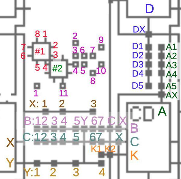
    The first two columns of the table indicate the switch matrices. There are two switch matrices, labeled #1 (red) and #2 (green) in my diagram below. The 8 pins on matrix #1 are labeled 1-8 clockwise. (Switch #2 is the same, but there wasn't room for the labels.) For example, "#2: 1-3" indicates that bit connects pins 1 and 3 on switch #2. The next column defines the "ND" non-directional connections, the boxes below with purple numbers near the switch matrices. Each ND bit in the table controls the corresponding ND connection.

    Diagram of the interconnect showing the numbering scheme I made up for the bitstream table.

    Diagram of the interconnect showing the numbering scheme I made up for the bitstream table.

    The next two columns describe what I'm calling the PIP connections, the solid boxes on lines above. The connections from output X (brown) are controlled by individual bits (X1, X2, C3). Likewise, the connections from output Y (yellow). The connections to input B (light purple) are different. Only one of these input connections can be active at a time, so they are encoded with multiple bits using the multiplexer scheme. Inputs C (cyan), D (blue) and A (green) are similar. The remaining table columns describe the CLB; refer to the datasheet for details. Bits control the clock, set and reset lines. The X and Y outputs can be selected from the F or G LUTs. The last two columns define the LUTs. There are three inputs for LUT F and three inputs for LUT G, with multiplexers controlling the inputs. Finally, the 8 bits for each LUT are defined, specifying the output for a particular combination of three inputs. 

  12. Various FPGA patents provide some details on the chips: 4870302, 4642487, 4706216, 4758985, and RE34363. XACT documentation was formerly at Xilinx, but they seem to have removed it. It can now be found here. John McMaster has some xc2064 tools available. 

Using an FPGA to generate raw VGA video:FizzBuzz with animation

This blog post shows how you can generate a video signal with an FPGA, using the FizzBuzz problem as an example. Creating video with an FPGA was easier than I expected, simpler than my previous serial-line FizzBuzz on an FPGA. I got a bit carried away with the project and added animation, rainbow text and giant bouncing words to the display.

FizzBuzz from an FPGA board. The board generates raw VGA video output with the results animated, along with the words "Fizz" and "Buzz" that bounce around the screen.

FizzBuzz from an FPGA board. The board generates raw VGA video output with the results animated, along with the words "Fizz" and "Buzz" that bounce around the screen.

If you're not familiar with the "FizzBuzz test", the problem is to write a program that prints the numbers from 1 to 100, except multiples of 3 are replaced with the word "Fizz", multiples of 5 with "Buzz" and multiples of both with "FizzBuzz". Since FizzBuzz can be implemented in a few lines of code, it can be used as an interview question to weed out people who can't program at all. But it's much more of a challenge on an FPGA.

An FPGA (Field-Programmable Gate Array) is an interesting chip that you can program to implement arbitrary digital logic. This lets you build a complex digital circuit without wiring up individual gates and flip flops. It's like having a custom chip that can be anything from a logic analyzer to a microprocessor to a video generator. For this project, I used the Mojo FPGA board (below).

The Mojo FPGA board. The Spartan-6 FPGA chip dominates the board.

The Mojo FPGA board. The Spartan-6 FPGA chip dominates the board.

Generating the VGA signals

There's a learning curve to an FPGA, since you're designing circuits, not writing software that runs on a processor. But if you can blink five LEDs with an FPGA, you're most of the way to creating a VGA video signal. The VGA video format is a lot simpler than I expected: just three signals for the pixels (red, green and blue), and two signals for horizontal sync and vertical sync.

The basic idea is to use two counters: one to count pixels horizontally and one to count lines vertically. At each spot on the screen, the desired pixel color is generated from these coordinates. In addition, the horizontal and vertical sync signals are produced when the counters are at the right positions. I used the basic 640x480 VGA screen resolution2 which requires counting to 800 and 525.111 Horizontally, there are 800 pixels for each line: 640 visible image pixels, followed by 16 blank pixels, 96 pixels of horizontal sync and 48 more blank pixels. (There are historical reasons for these strange numbers.) Meanwhile, the vertical counter must count out 525 lines: 480 image lines, 10 blank lines, 2 lines of vertical sync and 33 more blank lines.

Putting this all together, I created a vga module (source) to generate the VGA signals. This code is in Verilog (a standard language for FPGAs); I won't explain Verilog thoroughly, but hopefully enough to show how it works. The code below implements the x and y counters. The first line indicates action is taken on the positive edge of each (50 MHz) clock signal. The next line toggles clk25 each clock, creating the 25 MHz signal we'll use for the pixel clock. (One confusing thing is that <= indicates assignment, not comparison.) The code increments the x counter from 0 to 799. At the end of each line, y is incremented, running from 0 to 524. Thus, this code generates the necessary pixel and line counters.

always @(posedge clk) begin
  clk25 <= ~clk25;
  if (clk25 == 1) begin
    if (x < 799) begin
      x <= x + 1;
    end else begin
      x <= 0;
      if (y < 524) begin
    y <= y + 1;
      end else begin
    y <= 0;
      end
    end
  end
end

While Verilog code looks like a standard programming language, its effects are very different. This code doesn't generate instructions that are executed sequentially by a processor, but instead causes circuitry to be instantiated in the FPGA chip. It creates registers from flip flops for clk25, x and y. Binary adders are generated to increment x and y. The if statements turn into logic gate comparators controlling the registers. All this circuitry runs in parallel, triggered by the 50 MHz clock. To understand FPGAs, you need to get out of the sequential program mindset and think of the underlying circuits.

Getting back to the vga module, the horizontal and vertical sync signals are generated from the x and y counters by the code below. In addition, a valid flag indicates the 640x480 region where a video signal should be generated; the screen must be blank outside this region. As before, these Verilog statements are generating logic gates to test the conditions, not creating code.

assign hsync = x < (640 + 16) || x >= (640 + 16 + 96);
assign vsync = y < (480 + 10) || y >= (480 + 10 + 2);
assign valid = (x < 640) && (y < 480);

The "useful" part of the VGA signal is the red, green, and blue pixel signals that control what appears on the screen. To test everything out, I wrote a few lines to turn r, g and b on for various regions of the screen, blanking them all outside the visible (`valid`) area.3 (The question mark is the ternary conditional operator, as in Java)

if (valid) begin
  rval = (x < 120 || x > 320) ? 1 : 0;
  gval = (y < 240 || y > 360) ? 1 : 0;
  bval = (x > 500 && (y < 120 || y > 300)) ? 1 : 0;
end else begin
  rval = 0;
  gval = 0;
  bval = 0;
end

I ran the code on my FPGA board and nothing happened—the monitor stayed black and I wondered what went wrong. Fortunately, after a couple seconds4 the monitor completed its normal startup cycle and displayed the output. I was pleasantly surprised that VGA output worked the first time, even if the output was just arbitrary blocks of color.5

My first VGA program produced random color blocks on the screen. Not very meaningful, but it showed that everything worked.

My first VGA program produced random color blocks on the screen. Not very meaningful, but it showed that everything worked.

Putting characters on the screen

The next step was to display text characters on the screen. I implemented a character generation module to provides the pixels for an 8x8 character. Rather than include the full ASCII character set, I only used the characters necessary for FizzBuzz: 0 through 9, "B", "F", "i", "u", "z" and blank. Conveniently, this worked out to 16 character values, fitting into a 4-bit input.

Thus, the module takes a 4-bit character code and a 3-bit row number (for the 8 lines of each character) and outputs 8 pixels for that row of the character. The code (excerpt below, full code here) is simply a big case statement to output the appropriate bits.6 This code essentially compiles into a ROM, which is implemented in the FPGA by lookup tables.

case ({char, rownum})
  7'b0000000: pixels = 8'b01111100; //  XXXXX  
  7'b0000001: pixels = 8'b11000110; // XX   XX 
  7'b0000010: pixels = 8'b11001110; // XX  XXX 
  7'b0000011: pixels = 8'b11011110; // XX XXXX 
  7'b0000100: pixels = 8'b11110110; // XXXX XX 
  7'b0000101: pixels = 8'b11100110; // XXX  XX 
  7'b0000110: pixels = 8'b01111100; //  XXXXX  
  7'b0000111: pixels = 8'b00000000; //

  7'b0001000: pixels = 8'b00110000; //   XX    
  7'b0001001: pixels = 8'b01110000; //  XXX    
  7'b0001010: pixels = 8'b00110000; //   XX    
  7'b0001011: pixels = 8'b00110000; //   XX    
  7'b0001100: pixels = 8'b00110000; //   XX    
  7'b0001101: pixels = 8'b00110000; //   XX    
  7'b0001110: pixels = 8'b11111100; // XXXXXX  
...

I updated the top-level program to use the low bits of the X pixel position for the character and pixel index, and the low bits of the Y pixel position for the row index. The results can be seen below; I've magnified the text in the red box so you can see the characters.

My first implementation of text. (Zoomed region in red.) Due to a bug, all the characters are backwards.

My first implementation of text. (Zoomed region in red.) Due to a bug, all the characters are backwards.

Oops, I implemented the character generator with bit 7 on the left, while the pixel index values have bit 7 on the right, so the characters were displayed backwards. But a quick fix got the characters to display correctly.

Generating a line of FizzBuzz

Once I could display characters, I needed to provide the right characters for the FizzBuzz output. The algorithm is the same as my previous FizzBuzz program, so I'll just give the highlights here.

Converting the numbers from 1 to 100 into characters is trivial on a microprocessor, but more difficult with digital logic since there's no built-in divide operation; dividing by 10 and 100 requires many logic gates. My solution was to use a binary-coded decimal (BCD) counter, using a separate 4-bit counter for each digit.

The next challenge was testing if the number was divisible by 3 or 5. As with division, the modulo operation is easy on a microprocessor, but hard with digital logic. Instead of computing modulo values, I used counters for the value modulo 3 and the value modulo 5. The value modulo 3, for instance, simply counts 0, 1, 2, 0, 1, 2, ... (See the footnote for other approaches.7)

A FizzBuzz output line can be up to 8 characters long. The `fizzbuzz` module (source) outputs the appropriate eight 4-bit characters as a 32-bit variable line. (The normal way to generate video would be to store all the screen's characters or pixels into video RAM, but I decided to generate everything dynamically.) An if statement (excerpt below) updates the bits of line to return "Fizz", "Buzz", "FizzBuzz" or the number as appropriate.

if (mod3 == 0 && mod5 != 0) begin
  // Fizz
  line[3:0] <= CHAR_F;
  line[7:4] <= CHAR_I;
  line[11:8] <= CHAR_Z;
  line[15:12] <= CHAR_Z;
end else if (mod3 != 0 && mod5 == 0) begin
  // Buzz
  line[3:0] <= CHAR_B;
  line[7:4] <= CHAR_U;
  line[11:8] <= CHAR_Z;
  line[15:12] <= CHAR_Z;
...

The FizzBuzz module needed a signal to increment the counts to the next number so I modified the vga module to indicate the start of a new line and used this to move to the next number. When I tried my code, I got very strange output with alien symbols; the photo below shows a detail.

Changing the character every row yields mysterious symbols, not the desired characters.

Changing the character every row yields mysterious symbols, not the desired characters.

The bug was that I was moving to the next FizzBuzz value after every line of pixels instead of waiting 8 lines to draw a full character. Thus, each displayed character consisted of slices from 8 different characters. Incrementing the FizzBuzz counter every 8 lines instead of every line fixed this problem, as you can see below. (Debugging VGA code is much easier than other FPGA things, since problems are visible on the screen. You don't need to poke around with an oscilloscope trying to figure out what went wrong.)

The FizzBuzz output, as displayed on a VGA monitor.

The FizzBuzz output, as displayed on a VGA monitor.

At this point I had the FizzBuzz output appearing on the screen, but the static display was kind of boring. Changing the foreground and background color of each row was easy—just using some bits of the Y value for the red, green and blue colors. This yielded colored text with a 1980s PC aesthetic.

With the foreground and background colors based on the line, the text is more interesting.

With the foreground and background colors based on the line, the text is more interesting.

Next, I added some basic animation. The first step was to add an output from the vga module to indicate when the screen was redrawn, a new field every 60th of a second. I used this to change the colors dynamically. (Tip: don't flash the screen color every 60th of a second unless you want a headache; use a counter and change it less often.)

Trying out different graphical effects is fun and addictive, since you get immediate feedback. I decided to have the "Fizz" and "Buzz" lines slide across the screen with a rainbow color trail (inspired by Nyan Cat). To do this, I changed the character's start position based on a counter. For the rainbow color effect, I selected the color based on the row number (so each row of the character could have a different color) and added the rainbow trail.

A closeup of the final output.

A closeup of the final output.

The final effect I added was giant words "Fizz" and "Buzz" that bounced around the screen. The bouncing effect was based on a bouncing invisible box (inspired by FPGA Pong) that held the word.8 A variable dx keeps track of the X direction and dy keeps track of the Y direction. On each new screen (i.e. 60 times a second), the box's X and Y coordinates are incremented or decremented based on the direction variables. If the box reaches the right or left edges, dx is toggled. Similarly, dy is toggled if the box reaches the top or bottom. The big text is then drawn inside the box using another instantiation of the character generator described earlier. The word is enlarged by a factor of 8 by dropping the three low-order bits from the coordinate. You're probably tired of Verilog code by now so I won't show the code here, but it's on github. The final result is shown in the video clip below.

Hardware details

For this project, I used the Mojo V3 FPGA board development board (below), which was designed to be an easy-to-use starter board. It uses an FPGA chip from Xilinx's Spartan 6 family. Although the Mojo uses one of the smallest Spartan 6 chips, the chip still contains over 9000 logic cells and 11,000 flip flops, so it can do a lot. (For other options, see this list of cheap FPGA boards.)

Interfacing the FPGA board to VGA is almost trivial: just three 270&ohm; resistors. The perf board is just to attach the cable to a header.

Interfacing the FPGA board to VGA is almost trivial: just three 270Ω resistors. The perf board is just to attach the cable to a header.

If you want to use VGA, it's easier to use a development board that includes a VGA connector. But if your board lacks a connector (like the Mojo), adding VGA is straightforward. Simply put 270Ω resistors between the FPGA's red, green and blue output pins and the VGA connection. The horizontal and vertical sync can be wired directly from the FPGA.9

I used Xilinx's development environment (called ISE) to write and synthesize the Verilog code. (For details on writing code and getting it onto the FPGA board, see my previous FPGA article.) To specify which physical FPGA pins to use, I added lines to the mojo.ucf configuration file. This maps the red output pin_r to pin 50 on the board, and so forth.

NET "pin_r" LOC = P50 | IOSTANDARD = LVTTL;
NET "pin_g" LOC = P40 | IOSTANDARD = LVTTL;
NET "pin_b" LOC = P34 | IOSTANDARD = LVTTL;
NET "pin_hsync" LOC = P32 | IOSTANDARD = LVTTL;
NET "pin_vsync" LOC = P29 | IOSTANDARD = LVTTL;

Driving VGA from an FPGA is common, so you can find lots of similar projects on the web such as FPGA Pong, 24-bit color using a DAC chip, the Basys 3 board and displaying an image. If you want a schematic, see this page. The book Programming FPGAs has a whole chapter on VGA.

Understanding the VGA format

The VGA video format may seem a bit strange, but looking at the history of television and the CRT (cathode ray tube) provides context. In a CRT, a beam of electrons scans across the screen, lighting up the phosphor coating to produce an image. Scanning happens in a raster pattern: the beam scans across the screen left-to-right, and then a horizontal sync pulse causes the beam to rapidly return to the left during the horizontal retrace. The process repeats line-by-line until the bottom of the screen, when a vertical sync pulse triggers vertical retrace and the beam returns to the top. During the horizontal and vertical retrace, the beam is blanked so retrace doesn't draw lines on the screen. The diagram below illustrates the raster scan pattern.

Raster scan pattern for a CRT. (Wikipedia)

Raster scan pattern for a CRT. (Wikipedia)

These characteristics carried over to VGA, resulting in the horizontal and vertical sync pulses, and the long intervals during which the video must be blanked.

In 1953, the NTSC standard for color television was introduced.10 VGA, however, is much simpler than NTSC since it uses five wires for the sync and color signals, instead of cramming everything into a single signal with a complex encoding. One strange feature of NTSC that carries over to VGA is the screen refresh rate isn't the claimed 60 Hertz, but actually 59.94 Hertz.11

The oscilloscope trace below shows the VGA video signals across two lines. The horizontal sync pulses (yellow) indicate the start of each line. The brief red, green and blue pulses near the start of the line are white pixels from a FizzBuzz number. The red signal near the middle of the line is the floating red word "Buzz".

Oscilloscope trace of VGA signals, showing red, green, blue and horizontal sync.

Oscilloscope trace of VGA signals, showing red, green, blue and horizontal sync.

Conclusion

Driving a VGA monitor from an FPGA was much easier than I expected, but I certainly wouldn't get hired if I encountered FizzBuzz as an FPGA interview question! If you're interested in FPGAs, I highly recommend playing around with video output. It's not much harder than blinking an LED and much more rewarding. Creating video output is also much more fun than debugging with an oscilloscope—you get immediate visual feedback and even if things go wrong, they are often entertaining.

Follow me on Twitter or RSS to find out about my latest blog posts. My FPGA code is on github.

Notes and references

  1. The VGA signal is supposed to have a 25.175 MHz pixel clock. Instead, I divided the Mojo board's 50 MHz clock by 2 to get a 25 MHz clock. The VGA standard says that the pixel clock must be 25.175 MHz ± 0.5%. A clock rate of 25 MHz is off by 0.7% so technically is a bit off from the spec. However, monitors are designed to handle signals generated by cheap graphics cards, so they will usually manage to display whatever you throw at them. 

  2. The detailed timings for dozens of standard video resolutions can be found here. Page 17 has the 640x480 60 Hz resolution I used. 

  3. When I forgot to blank the pixels outside the valid screen area, the monitor still managed to display an image, but it was very dim because the monitor got confused about what voltage represented "dark". Just a tip in case you find your display mysteriously darkened. 

  4. It's kind of amazing if you think about what an LCD monitor needs to do in order to display a VGA image designed for a CRT. The monitor has to examine the incoming signals to "guess" what video resolution a computer is sending to it. Then it needs to resample the video signal to match the resolution of the LCD panel. Finally, it sends the new pixel data to the LCD. 

  5. For some reason, the output was shifted down about 25 pixels. It worked fine on a different monitor, so I'm not sure if was just something with my monitor's alignment or if I had a bug. I could adjust this by making the vertical sync pulse 25 rows later. 

  6. It would be tedious to type all the code for character generation, so I wrote a Python program to create the Verilog code from a font file. The original font is here

  7. After my last FPGA FizzBuzz, people suggested some other approaches so I tried them out on the VGA project. With modulo counters (my original approach), the entire project used 276 LUTs (lookup tables) and 277 flip flops. One suggestion was to use ring counters (i.e. one shifted bit) instead of binary counters for the modulo counters. This used 277 LUTs and 281 flip flops, so slightly worse. Another suggestion was to add the digits and take the modulo 3 value. The logic to add and perform modulo brought the count to 305 LUTs, much worse. Adding the modulo 3 values (instead of digits) brought it down to 289 LUTs, still worse. 

  8. The big floating words are essentially sprites—bitmaps that can be arbitrarily positioned on the screen. Sprites were popular with video games and computers in the 1970s and early 1980s such as Pacman, Atari and Commodore 64. Sprites let slow processors perform animation; instead of moving all the pixels around in memory, the processor would just update the sprite coordinates. The top-level code (source) ties together all the pieces and combines everything onto the screen: the text, the rainbow trail, the giant "Fizz" (in a rainbow pattern) and the giant "Buzz" (in red). 

  9. To connect to the VGA monitor, I cut a VGA cable in half and connected its wires to the FPGA board, reusing the cable from my project to read monitor data using I2C. Don't take this approach—the tiny wires inside are difficult to solder and break easily. Instead, just use a VGA connector. The interface to VGA is simply three 270Ω resistors, to get the right voltages for the red, green and blue signals. You can use more resistors to get more colors, essentially building 2-bit or more A/D converters. 

  10. NTSC was a remarkably clever way to introduce color, while remaining compatible with black-and-white televisions. However, it is very hard to understand. I was scared off from video by the talk of encoding color with phase and quadrature and a color subcarrier synced to a color burst signal. Because NTSC combines the color and sync signals into a single broadcast signal, the encoding is much more complex than VGA. 

  11. While monitors say they have a 60 Hz refresh rate, the actual refresh rate is 59.94 Hz, a strange frequency dating back to the origins of color television. A screen refresh frequency of 60 Hz was desirable to cancel out power line interference. However, to prevent the color carrier frequency from interfering with the audio frequency, various frequencies had to be adjusted, resulting in the screen refresh frequency of 59.94 Hertz. It almost seems like numerology, but the frequency choices are explained in detail in this video and in Wikipedia

Implementing FizzBuzz on an FPGA

I recently started FPGA programming and figured it would be fun to use an FPGA to implement the FizzBuzz algorithm. An FPGA (Field-Programmable Gate Array) is an interesting chip that you can program to implement arbitrary digital logic. This lets you build a complex digital circuit without wiring up individual gates and flip flops. It's like having a custom chip that can be anything from a logic analyzer to a microprocessor to a video generator.

The "FizzBuzz test" is to write a program that prints the numbers from 1 to 100, except multiples of 3 are replaced with the word "Fizz", multiples of 5 with "Buzz" and multiples of both with "FizzBuzz". Since FizzBuzz can be implemented in a few lines of code, it is used as a programming interview question to weed out people who can't program at all.

The Mojo FPGA board, connected to a serial-to-USB interface. The big chip on the Mojo is the Spartan 6 FPGA.

The Mojo FPGA board, connected to a serial-to-USB interface. The big chip on the Mojo is the Spartan 6 FPGA.

Implementing FizzBuzz in digital logic (as opposed to code) is rather pointless, but I figured it would be a good way to learn FPGAs.1 For this project, I used the Mojo V3 FPGA development board (shown above), which was designed to be an easy-to-use starter board. It uses an FPGA chip from Xilinx's Spartan 6 family. Although the Mojo's FPGA is one of the smallest Spartan 6 chips, it still contains over 9000 logic cells and 11,000 flip flops, so it can do a lot.

Implementing serial output on the FPGA

What does it mean to implement FizzBuzz on an FPGA? The general-purpose I/O pins of an FPGA could be connected to anything, so the FizzBuzz output could be displayed in many different ways such as LEDs, seven-segment displays, an LCD panel, or a VGA monitor. I decided that outputting the text over a serial line to a terminal was the closest in spirit to a "standard" FizzBuzz program. So the first step was to implement serial output on the FPGA.

The basic idea of serial communication is to send bits over a wire, one at a time. The RS-232 serial protocol is a simple protocol for serial data, invented in 1960 for connecting things like teletypes and modems. The diagram below shows how the character "F" (binary 01000110) would be sent serially over the wire. First, a start bit (low) is sent to indicate the start of a character.2 Next, the 8 bits of the character are sent in reverse order. Finally, a stop bit (high) is sent to indicate the end of the character. The line sits idle (high) between characters until another character is ready to send. For a baud rate of 9600, each bit is sent for 1/9600 of a second. With 8 data bits, no parity bit, and 1 stop bit, the protocol is known as 8N1. Many different serial protocols are in use, but 9600 8N1 is a very common one.

Serial line output of the character "F" sent at 9600 baud / 8N1.

Serial line output of the character "F" sent at 9600 baud / 8N1.

The first step in implementing this serial output was to produce the 1/9600 second intervals for each bit. This interval can be measured by counting 5208 clock pulses on the Mojo.3 I implemented this by using a 13-bit counter to repeatedly count from 0 to 5207. To keep track of which bit is being output in each interval, I used a simple state machine that advanced through the start bit, the 8 data bits, and the stop bit. The state is held in a 4-bit register. (With FPGAs, you end up dealing a lot with clock pulses, counters, and state machines.)

To create the interval and state registers in the FPGA chip, I wrote code in the Verilog hardware description language. I won't explain Verilog thoroughly, but hopefully you can get a feel for how it works. In the code below, the first lines define a 13-bit register called counter and a 4-bit register called state. The counter is incremented until it reaches 5207, at which time the counter is reset to 0 and state is incremented to process the next output bit. (Note that <= is an assignment operator, not a comparison.4) The line always @(posedge clk) indicates that the code is executed on the positive edge of each clock.

reg [12:0] counter;
reg [3:0] state;

always @(posedge clk) begin
  if (counter < 5207) begin
     counter <= counter + 1;
  end else begin
    counter <= 0;
    state <= state + 1;
  end
end

While this may look like code in a normal programming language, it operates entirely differently. In a normal language, operations usually take place sequentially as the program is executed line by line. For instance, the processor would check the value of counter. It would then add 1 to counter. But in Verilog, there's no processor and no program being executed. Instead, the code generates hardware to perform the operations. For example, an adder circuit is created to increment counter, and a separate adder to increment state, and additional logic for the comparison with 5207. Unlike the sequential processor, the FPGA does everything in parallel. For instance, the FPGA does the 5207 comparison, the increment or reset of counter and the increment of state all in parallel on each clock pulse. Because of this parallelism, FPGAs can be much faster than processors for highly parallel tasks.

The next part of the serial code (below) outputs the appropriate bit for each state. As before, while this looks like a normal programming language, it is generating hardware circuits, not operations that are executed sequentially. In this case, the code creates gate logic (essentially a multiplexer) to select the right value for out.

case (state)
  IDLE: out = MARK; // high
  START: out = SPACE; // low
  BIT0: out = char1[0];
  BIT1: out = char1[1];
  ...
  BIT6: out = char1[6];
  STOP: out = MARK;
  default: out = MARK;
endcase

There's a bit more code for the serial module to define constants, initialize the counters, and start and stop each character, but the above code should give you an idea of how Verilog works. The full serial code is here.

The FizzBuzz Algorithm

The next step is figuring out what to send over the serial line. How do we convert the numbers from 1 to 100 into ASCII characters? This is trivial when programming a microprocessor, but hard with digital logic. The problem is that converting a binary number to decimal digits requires division by 10 and 100, and division is very inconvenient to implement with gates. My solution was to use a binary-coded decimal (BCD) counter, storing each of the three digits separately. This made the counter slightly more complicated, since each digit needs to wrap at 9, but it made printing the digits easy.

I wrote a BCD counter module (source) to implement the 3-digit counter. It has three 4-bit counters digit2, digit1, and digit0. The flag increment indicates that the counter should be incremented. Usually just digit0 is incremented. But if digit0 is 9, then it wraps to 0 and digit1 is incremented. Except if digit1 is also 9, then it wraps to 0 and digit2 is incremented. Thus, the digits will count from 000 to 999.

if (increment) begin
  if (digit0 != 9) begin
    // Regular increment digit 0
    digit0 <= digit0 + 1;
  end else begin
    // Carry from digit 0
    digit0 <= 0;
    if (digit1 != 9) begin
      // Regular increment digit 1
      digit1 <= digit1 + 1;
    end else begin
      // Carry from digit 1
      digit1 <= 0;
      digit2 <= digit2 + 1;
    end
  end
end

As before, keep in mind that while this looks like normal program code, it turns into a bunch of logic gates, generating the new values for digit2, digit1 and digit0 on each clock cycle. The system isn't executing instructions in sequence, so performance isn't limited by the number of instructions but just by the delay for signals to propagate through the gates.

The next challenge was testing if the number was divisible by 3 or 5. Like division, the modulo operation is easy on a microprocessor, but hard with digital logic. There's no built-in divide operation, so modulo needs to be computed with a big pile of gates. Although the IDE can synthesize the gates for a modulo operation, it seemed inelegant. Instead, I simply kept counters for the value modulo 3 and the value modulo 5. The value modulo 3, for instance, would simply count 0, 1, 2, 0, 1, 2, ...5

The final piece of FizzBuzz was the code to output each line, character by character. In a program, we could simply call the serial output routine for each character. But in an FPGA, we need to keep track of which character is being sent, with yet another state machine. Note that to convert each digit to an ASCII character, binary 11 is concatenated, using the slightly strange syntax 2'b11. The code excerpt below is slightly simplified; the full code includes leading zero checks so "001" will print as "1".

state <= state + 1; // Different state from serial
if (mod3 == 0 && mod5 != 0) begin
  // Fizz
  case (state)
   1: char <= "F";
   2: char <= "i";
   3: char <= "z";
   4: char <= "z";
   5: char <= "\r";
   6: begin
     char <= "\n";
     state <= NEXT; // Done with output line
     end
  endcase
end else if (mod3 != 0 && mod5 == 0) begin
  ... Buzz case omitted ...
end else if (mod3 == 0 && mod5 == 0) begin      
 ... Fizzbuzz case omitted ...
end else begin 
  // No divisors; output the digits of the number.
  case (state)
    1: char <= {2'b11, digit2[3:0]};
    2: char <= {2'b11, digit1[3:0]};
    3: char <= {2'b11, digit0[3:0]};
    4: char <= "\r";
    5: begin
     char <= "\n";
     state <= NEXT;
    end
  endcase
end

Putting it all together, there are multiple state machines and counters controlling the final FizzBuzz circuit. The main state machine controls the code above, moving through the characters of the line. For each character, this state machine triggers the serial output module, and waits until the character has been output. Inside the serial module, a state machine moves through each bit of the character. This state machine waits until the baud rate counter has measured out the width of the bit. When the serial output of the character is done, the serial module signals the main state machine. The main state machine then moves to the next character in the line. When the line is done, the main state machine increments the BCD counter (counting from 1 to 100) and then starts outputting the next line.

Programming languages make it easy to do operations in sequence, perform loops, make subroutine calls and so forth. But with an FPGA, you need to explicitly control when things happen, using state machines and counters to keep track of what's happening. In exchange for this, FPGAs give you a huge degree of parallelism and control.

Running FizzBuzz on the FPGA board

To compile the Verilog code, I used Xilinx's ISE tool (below), which is a development environment that lets you write code, simulate it, and synthesize it into gate-level circuitry that can be loaded onto the FPGA. Using the ISE tool is fairly straightforward, and explained in the Mojo tutorials. The synthesis process was slow compared to a compile, taking about 45 seconds for my FizzBuzz program.

By writing Verilog code in Xilinx's ISE tool, you can program functionality into an FPGA.

By writing Verilog code in Xilinx's ISE tool, you can program functionality into an FPGA.

Once I had the code working in the simulator,7, I downloaded it to the FPGA board over a USB cable. I connected the FPGA output pin to a USB-to-serial adapter6 and used a terminal emulator (screen) to display the serial output on my computer. I hit the reset button on the Mojo board and (after just a bit more debugging) the FizzBuzz output appeared (below).

First page of output from the FizzBuzz FPGA, as displayed by the screen terminal emulator.

First page of output from the FizzBuzz FPGA, as displayed by the screen terminal emulator.

The image below shows the raw serial data from the FPGA (yellow). This is the end result of the FizzBuzz circuitry running on the FPGA board—a sequence of pulses. The oscilloscope also shows the decoded ASCII characters (green). This data is near the beginning of the FizzBuzz output, showing the lines for 2, 3 and 4. (CR and LF are carriage return and line feed.)

The serial data signal (yellow) near the beginning of the FizzBuzz output. The ASCII decoding is in green.

The serial data signal (yellow) near the beginning of the FizzBuzz output. The ASCII decoding is in green.

What happens inside the FPGA?

You might wonder how a Verilog description of a circuit gets turned into digital logic, and how the FPGA implements this logic. The ISE synthesis tool turns the Verilog design into circuitry suitable for implementation inside the FPGA. It first synthesizes the Verilog code into a "netlist", specifying the logic and connections. Next it translates the netlists into FPGA primitives, which are mapped onto the capabilities of the particular chip (the Spartan 6 in my case). Finally, the place and route process optimizes the layout of the chip, minimizing the distance signals need to travel.

Schematic of the FizzBuzz circuit.

Schematic of the FizzBuzz circuit.

The image above shows the schematic of the FizzBuzz circuit, as generated by the synthesis tools. As you can see, the Verilog code turns into a large tangle of circuitry. Each block is a flip flop, logic element, multiplexer or other unit. These blocks make up the counters, state registers and logic for the FizzBuzz circuit. While this looks like a lot of logic, it used less than 2% of the chip's capability. A closeup (below) of the schematic shows a flip flop (labeled "fdre")8 and a lookup table (labeled "lut5") from the BCD counter. The nice thing about Verilog is that you can design the circuit at a high level, and it gets turned into the low-level circuitry. This is called RTL (Register-transfer level) and lets you design using registers and high-level operations on them, without worrying about the low-level hardware implementation. For instance, you can simply say count + 1 and this will generate the necessary binary adder circuitry.

Detail of the schematic showing a flip flop and lookup table.

Detail of the schematic showing a flip flop and lookup table.

The FPGA chip uses an interesting technique to implement logic equations. Instead of wiring together individual gates, the logic is implemented with a lookup table (LUT), which is a flexible way of implementing arbitrary logic. Each lookup table has 6 input lines, so it can implement any combinatorial logic with 6 inputs. With 6 inputs, there are 64 different input combinations, yielding a 64-line truth table. By storing this table as a 64-bit bitmap, the LUT can implement any desired logic function.

For example, part of the logic for the output pin is equivalent to the logic circuit below. This is implemented by storing the 64-bit value FFFFA8FFFFA8A8A8 into the lookup table. In the Spartan 6 chip, the LUT is implemented with 64 bits of static RAM, loaded when the FPGA is initialized. Since the chip has 5720 separate lookup tables, it can be programmed to implement a lot of arbitrary logic.

The gate logic implemented by one lookup table in the FPGA.

The gate logic implemented by one lookup table in the FPGA.

The final piece of the FPGA puzzle is the switch matrix that connects the circuitry together in arbitrary ways. In the Spartan 6 a handful of LUTs, flip flops and multiplexers are grouped into a configurable logic blocks (CLB).9 The CLBs are connected together by a switch matrix, as shown below. Each switch matrix block is programmed to connect different wires together, allowing the FPGA to be wired as desired. An important part of the FPGA synthesis process is positioning blocks to minimize the wiring distance, both to minimize signal propagation delay and to avoid running out of interconnect paths.

The switching matrix in the Spartan 6 FPGA allows arbitrary interconnections between CLBs. From the User Guide.

The switching matrix in the Spartan 6 FPGA allows arbitrary interconnections between CLBs. From the User Guide.

Should you try an FPGA?

Personally, I was very reluctant to try out an FPGA because they seemed scary and weird. While there is a learning curve, FPGAs aren't as difficult as I expected. If you're interested in new programming paradigms, FPGAs will definitely give you a different perspective. Things that you take for granted, such as performing operations in sequence, will move to the foreground with an FPGA. You can experiment with high degrees of parallelism. And FPGAs will give you a better idea of how digital circuits work.

However, I wouldn't recommend trying FPGAs unless you have some familiarity with wiring up LEDs and switches and understand basic digital logic: gates, flip flops, and state machines. If you're comfortable with an Arduino, though, an FPGA is a reasonable next step.

For most applications, a microcontroller can probably do the job as well as an FPGA and is easier to program. Unless you have high data rates or require parallelism, an FPGA is probably overkill. In my case, I found a microcontroller was barely powerful enough for my 3Mb/s Ethernet gateway project, so I'm looking into FPGAs for my next project.

Is the Mojo a good board to start with?

The Mojo FPGA development board is sold by Adafruit and Sparkfun, so I figured it would be a good hacker choice. The Mojo was designed for people getting started with FPGAs, and I found it worked well in this role. The makers of the Mojo wrote a solid collection of tutorials using Verilog.10 It was very helpful to use tutorials written for the specific board, since it minimized that amount of time I spent fighting with the board and tools. The Mojo is programmed over a standard USB cable, which is more convenient than boards that need special JTAG adapters.

The Mojo FPGA board. The Spartan-6 FPGA chip dominates the board.

The Mojo FPGA board. The Spartan-6 FPGA chip dominates the board.

Although the Mojo has plenty of I/O pins, it doesn't have any I/O devices included except 8 LEDs. It would be nicer to experiment with a board that includes buttons, 7-segment displays, VGA output, sensors and so forth. (It's not hard to wire up stuff to the Mojo, but it would be convenient to have them included.) Also, some development boards include external RAM but the Mojo doesn't, a problem for applications such as a logic analyzer that require a lot of storage.11 (You can extend the Mojo with an IO shield or RAM shield.)

A good introductory book to get started with the Mojo is Programming FPGAs; it also covers the considerably cheaper Papilo One and Elbert 2 boards. A list of FPGA development boards is here if you want to look at other options.

Conclusion

An FPGA is an impractical way to implement FizzBuzz, but it was a fun project and I learned a lot about FPGA programming. I certainly wouldn't get the FPGA job if FizzBuzz was used as an interview question, though! My code is on github, but keep in mind I'm a beginner to FPGAs.

Follow me on Twitter or RSS to find out about my latest blog posts.

Notes and references

  1. It's trivial to implement a microprocessor on an FPGA. For instance, with the Spartan 6 chip you can click a couple buttons in an IDE wizard and it will generate the circuitry for a MicroBlaze processor. Thus, the sensible way to run FizzBuzz on an FPGA would be to write the FizzBuzz code in a few lines of C, and then run it on a processor inside the FPGA. But that's too easy for me. 

  2. The start bit is necessary because otherwise the receiver couldn't tell when the character started, if the first bit sent was a 1. 

  3. Since the Mojo uses a 50 MHz clock, for 9600 baud each output bit is 50,000,000 / 9600 or approximately 5208 clocks wide. 9600 baud isn't a very fast rate so to challenge my circuit, I also tested it at 10M baud (by counting to 5 for each bit) and the circuit worked fine. (The USB-to-serial interface only worked up to 230400 baud, so I used oscilloscope decoding to check the higher speeds.) 

  4. In Verilog, <= is the nonblocking assignment operator, while = is the blocking assignment operator. Nonblocking assignments happen in parallel, and are generally used for sequential (clocked flip flop) logic. Blocking assignment is used for combinational (nonclocked) logic. This is a bit confusing but details are here

  5. I used BCD and not binary to store the number, so computing the value modulo 5 would have been almost trivial by looking at the last digit. But modulo 3 would still be difficult, so I stuck with the counter approach. 

  6. I couldn't connect the serial input directly to my computer, since it doesn't have a serial port. Instead, I used a USB-to-serial adapter, Adafruit's FTDI Friend. This adapter also had the advantage of accepting the FPGA's 3.3V signals, rather than the inconvenient +/- 15V used by genuine RS-232. 

  7. Debugging an FPGA is a very different process from software debugging. Since the FPGA is mostly a black box while running, you should test everything out in the simulator first, or else you end up in "FPGA Hell", blinking LEDs to figure out what's happening. To debug code, you simulate it by writing a "testbench", Verilog code that specifies various inputs at various times (example). You then run the simulator (below) and examine the output to make sure it is correct.

    The ISim simulator from Xilinx allows an FPGA design to be simulated.

    The ISim simulator from Xilinx allows an FPGA design to be simulated.

    If things go wrong, the simulator lets you step through the internal signals to find the problem. After testing everything in the simulator, my code only had trivial problems when I tried it on the real FPGA. My main problem was I assigned the serial output to the wrong pin on the board, so there was no output. 

  8. The Spartan 6 FPGA supports multiple types of flip flop. The FDRE is a D-Flip flop with synchronous Reset and clock Enable. 

  9. The Spartan 6 FPGA's configurable logic blocks (CLBs) are moderately complex, combining LUTs, 8 flip flops, wide multiplexers, carry logic, distributed RAM and shift registers. Hard-wiring components into the these blocks reduces flexibility slightly, but makes the switch matrix much simpler. The CLBs are described in detail in the CLB User Guide. The Spartan 6 FPGA also contains other types of blocks such as clock generation blocks and DSP blocks that can do fast 18-bit multiplication. 

  10. An alternative to the Verilog language is VHDL, which is also supported by the development environment. The Mojo also supports Lucid, a simpler FPGA language developed by the Mojo team. The Mojo Lucid tutorials explain the language, and there is a book available on Lucid. I decided I'd rather learn a standard language rather than Lucid though. 

  11. Although the Mojo doesn't have external RAM, its FPGA has 576 kilobits of internal RAM. This is tiny compared to boards with megabytes of external DRAM, though.