Intel released the powerful Pentium processor in 1993, establishing a long-running brand of high-performance processors.1
The Pentium includes a floating-point unit that can rapidly compute functions such as sines, cosines, logarithms, and exponentials.
But how does the Pentium compute these functions?
Earlier Intel chips used binary algorithms called CORDIC, but the Pentium switched to polynomials to approximate these transcendental functions much faster.
The polynomials have carefully-optimized coefficients that are stored in a special ROM inside the chip's floating-point unit.
Even though the Pentium is a complex chip with 3.1 million transistors, it is possible to see these transistors under a microscope and read out
these constants.
The first part of this post discusses how the floating point constant ROM is implemented in hardware.
The second part explains how the Pentium uses these constants to evaluate sin, log, and other
functions.
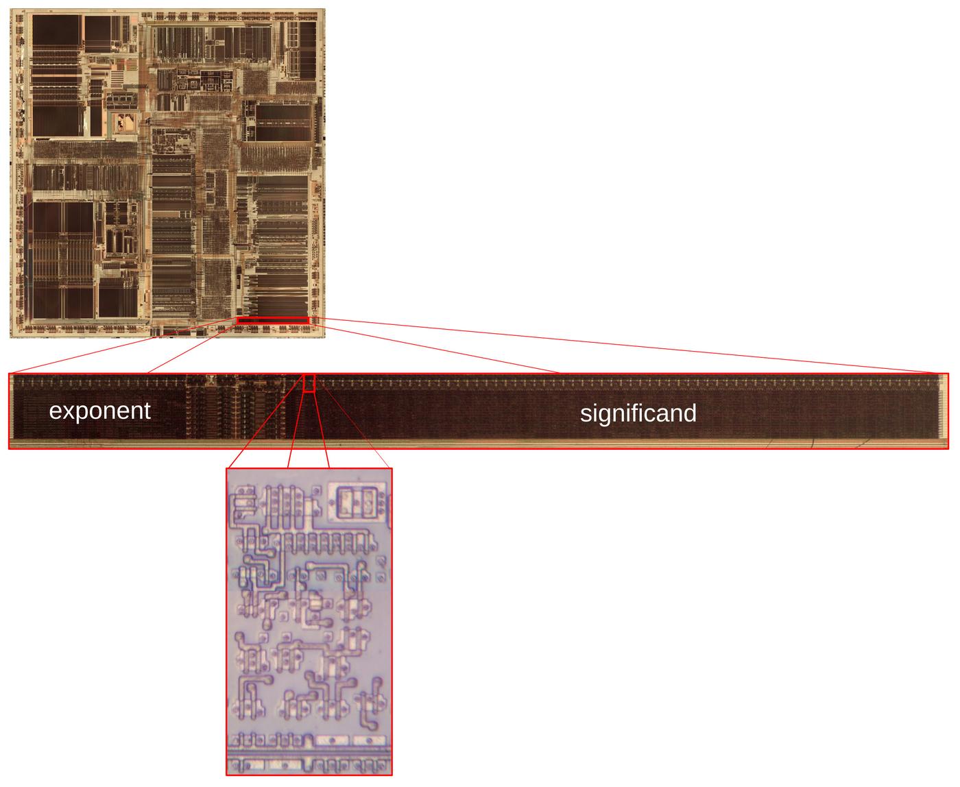
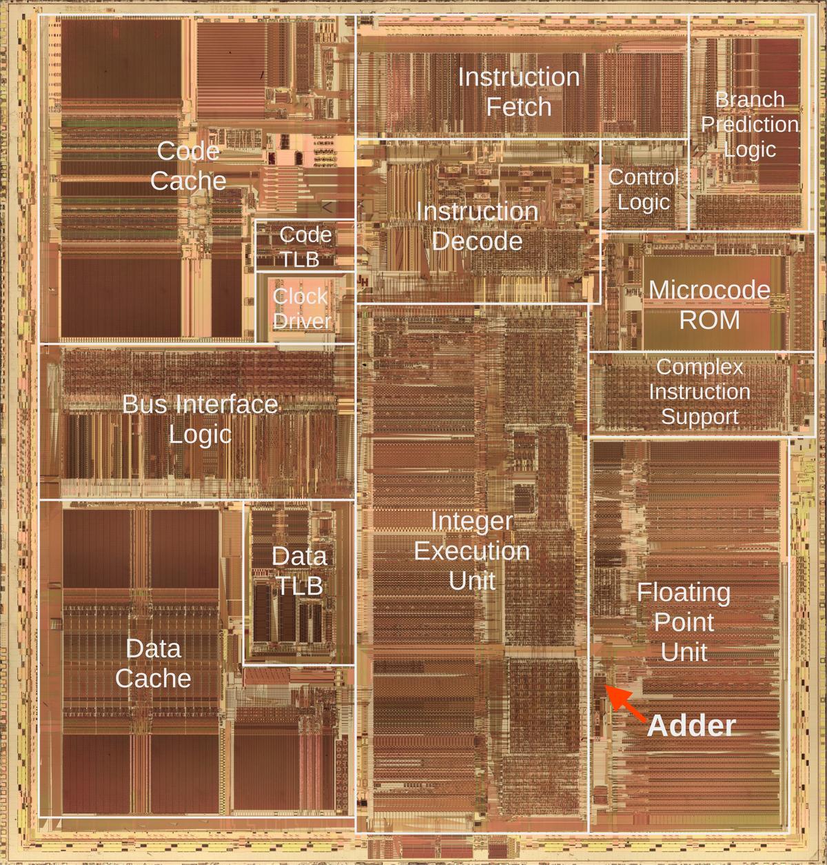
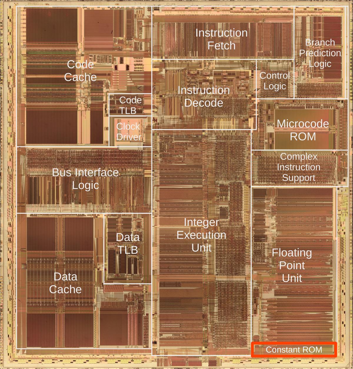
The photo below shows the Pentium's thumbnail-sized silicon die under a microscope.
I've labeled the main functional blocks; the floating-point unit is in the lower right.
The constant ROM (highlighted) is at the bottom of the floating-point unit.
Above the floating-point unit, the microcode ROM holds micro-instructions, the individual steps for complex
instructions. To execute an instruction such as sine, the microcode ROM directs the floating-point unit through
dozens of steps to compute the approximation polynomial using constants from the constant ROM.

Die photo of the Intel Pentium processor with the floating point constant ROM highlighted in red. Click this image (or any other) for a larger version.
Finding pi in the constant ROM
In binary, pi is 11.00100100001111110... but what does this mean?
To interpret this, the value 11 to the left of the binary point is simply 3 in binary. (The "binary point" is the
same as a decimal point, except for binary.)
The digits to the right of the binary point have the values 1/2, 1/4, 1/8, and so forth.
Thus, the binary value `11.001001000011... corresponds to 3 + 1/8 + 1/64 + 1/4096 + 1/8192 + ..., which matches the decimal value of pi.
Since pi is irrational, the bit sequence is infinite and non-repeating; the value in the ROM is truncated to 67 bits
and stored as a floating point number.
A floating point number is represented by two parts: the exponent and the significand.
Floating point numbers include very large numbers such as 6.02×10²³ and very small numbers such as 1.055×10⁻³⁴.
In decimal, 6.02×10²³ has a significand (or mantissa) of 6.02, multiplied by a power of 10 with an exponent of 23.
In binary, a floating point number is represented similarly, with a significand and exponent, except the significand is multiplied by a power of 2 rather than 10.
For example, pi is represented in floating point as 1.1001001...×21.
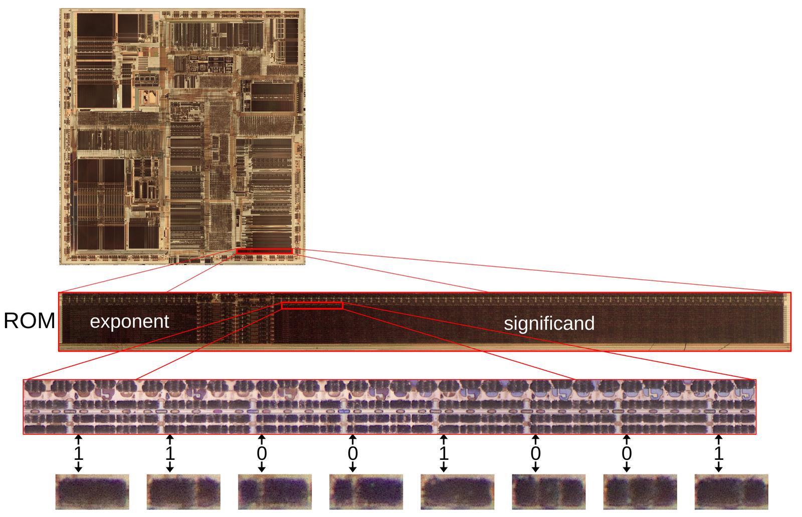
The diagram below shows how pi is encoded in the Pentium chip. Zooming in
shows the constant ROM.
Zooming in on a small part of the ROM shows the rows of transistors that store the constants.
The arrows point to the transistors representing the bit sequence 11001001, where a 0 bit is represented by a transistor (vertical white line) and a 1 bit is
represented by no transistor (solid dark silicon).
Each magnified black rectangle at the bottom has two potential transistors, storing two bits.
The key point is that by looking at the pattern of stripes, we can determine the pattern of transistors and thus the value
of each constant, pi in this case.

A portion of the floating-point ROM, showing the value of pi. Click this image (or any other) for a larger version.
The bits are spread out because each row of the ROM holds eight interleaved constants to
improve the layout.
Above the ROM bits, multiplexer circuitry selects the desired constant from the eight in the activated row.
In other words, by selecting a row and then one of the eight constants in the row, one of the 304 constants in the ROM is accessed.
The ROM stores many more digits of pi than shown here; the diagram shows 8 of the 67 significand bits.
Implementation of the constant ROM
The ROM is
built from MOS (metal-oxide-semiconductor) transistors, the transistors used in all modern computers.
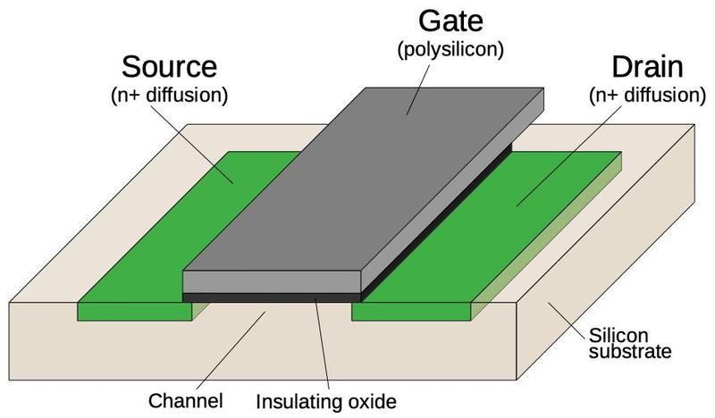
The diagram below shows the structure of an MOS transistor.
An integrated circuit is constructed from a silicon substrate.
Regions of the silicon are doped with impurities to create "diffusion" regions with desired electrical properties.
The transistor can be viewed as a switch, allowing current to flow between two diffusion regions called the source and drain.
The transistor is controlled by the gate, made of a special type of silicon called polysilicon.
Applying voltage to the gate lets current flow between the source and drain, which is otherwise blocked.
Most computers use two types of MOS transistors: NMOS and PMOS. The two types have similar construction but reverse the
doping; NMOS uses n-type diffusion regions as shown below, while PMOS uses p-type diffusion regions.
Since the two types are complementary (C),
circuits built with the two types of transistors are called CMOS.

Structure of a MOSFET in an integrated circuit.
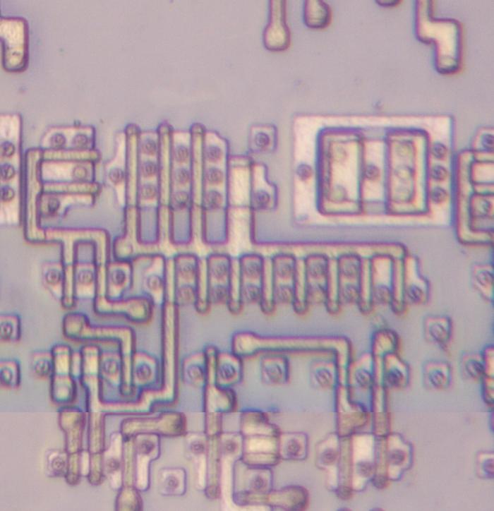
The image below shows how a transistor in the ROM looks under the microscope.
The pinkish regions are the doped silicon that forms the transistor's source and drain.
The vertical white line is the polysilicon that forms the transistor's gate.
For this photo, I removed the chip's three layers of metal, leaving just the underlying silicon and the polysilicon.
The circles in the source and drain are tungsten contacts that connect the silicon to the metal layer above.

One transistor in the constant ROM.
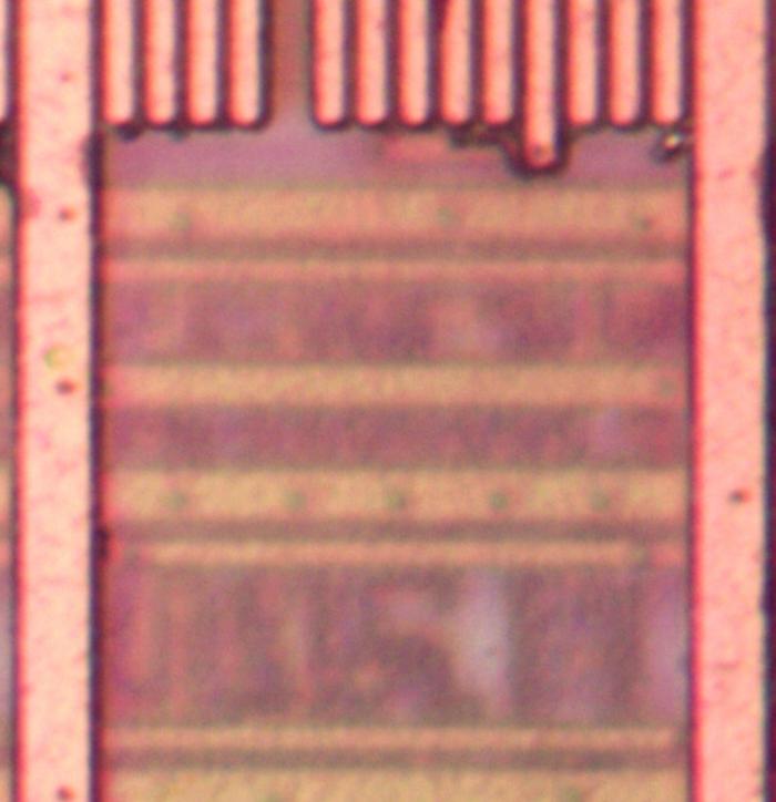
The diagram below shows eight bits of storage. Each of the four pink silicon rectangles has two potential transistors.
If a polysilicon gate crosses the silicon, a transistor is formed; otherwise there is no transistor.
When a select line (horizontal polysilicon) is energized, it will turn on all the transistors in that row.
If a transistor is present, the corresponding ROM bit is 0 because the transistor will pull the output line to ground. If a transistor
is absent, the ROM bit is 1.
Thus, the pattern of transistors determines the data stored in the ROM.
The ROM holds 26144 bits (304 words of 86 bits) so it has 26144 potential transistors.

Eight bits of storage in the ROM.
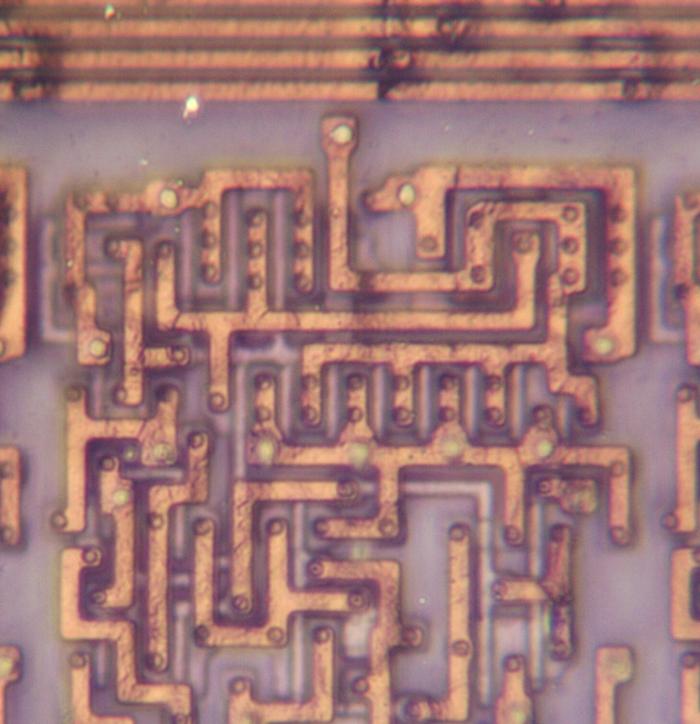
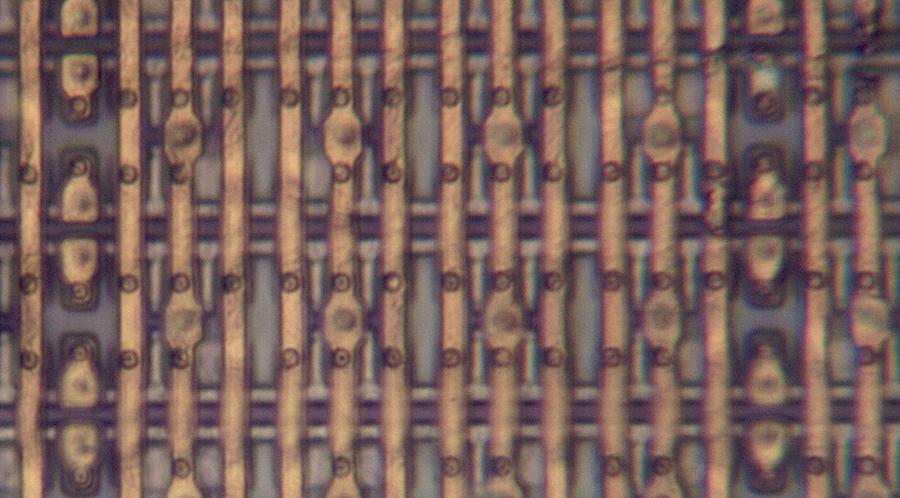
The photo below shows the bottom layer of metal (M1): vertical metal wires that provide the ROM outputs and
supply ground to the ROM.
(These wires are represented by gray lines in the schematic above.)
The polysilicon transistors (or gaps as appropriate) are barely visible between the metal lines.
Most of the small circles are tungsten contacts to the silicon or polysilicon; compare with the photo above.
Other circles are tungsten vias to the metal layer on top (M2), horizontal wiring that I removed for this photo.
The smaller metal "tabs" act as jumpers between the horizontal metal select lines in M2 and the
polysilicon select lines.
The top metal layer (M3, not visible) has thicker vertical wiring for the chip's primary distribution power and ground.
Thus, the three metal layers alternate between horizontal and vertical wiring, with vias between the layers.

A closeup of the ROM showing the bottom metal layer.
The ROM is implemented as two grids of cells (below): one to hold exponents and one to hold significands, as shown below.
The exponent grid (on the left) has 38 rows and 144 columns of transistors, while the significand grid (on the right) has 38 rows and 544 columns.
To make the layout work better, each row holds eight different constants; the bits are interleaved so the ROM holds the first bit of eight constants,
then the second bit of eight constants, and so forth.
Thus, with 38 rows, the ROM holds 304 constants; each constant has 18 bits in the exponent part and 68 bits in the significand section.

A diagram of the constant ROM and supporting circuitry. Most of the significand ROM has been cut out to make it fit.
The exponent part of each constant consists of 18 bits: a 17-bit exponent and one bit for
the sign of the significand and thus the constant.
There is no sign bit for the exponent because
the exponent is stored with 65535 (0x0ffff) added to it, avoiding negative values.
The 68-bit significand entry in the ROM consists of a mysterious flag bit2 followed by the 67-bit significand; the first bit of the significand is the integer part and the remainder is
the fractional part.3
The complete contents of the ROM are in the appendix at the bottom of this post.
To select a particular constant, the "row select" circuitry between the two sections activates one of the 38 rows. That row provides 144+544 bits to the selection
circuitry above the ROM.
This circuitry has 86 multiplexers; each multiplexer selects one bit out of the group of 8, selecting the desired constant.
The significand bits flow into the floating-point unit datapath circuitry above the ROM.
The exponent circuitry, however, is in the upper-left corner of the floating-point unit, a considerable distance from the ROM, so the exponent bits travel through a bus to the exponent circuitry.
The row select circuitry consists of gates to decode the row number, along with high-current drivers to energize
the selected row in the ROM.
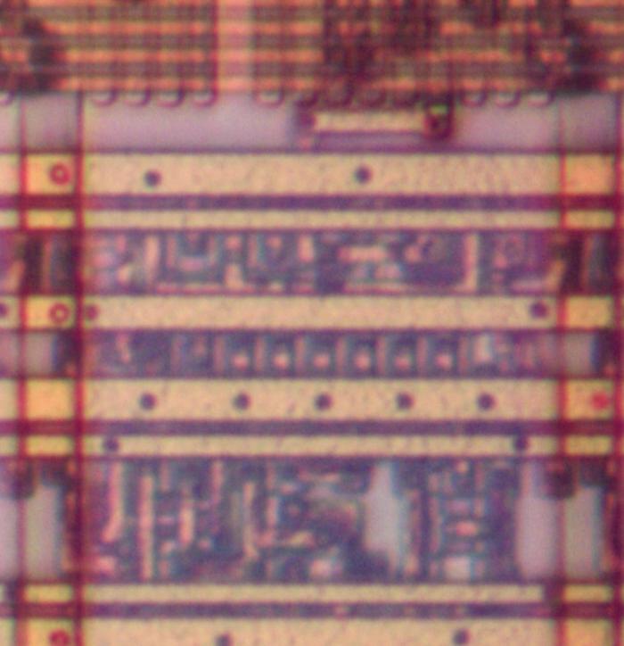
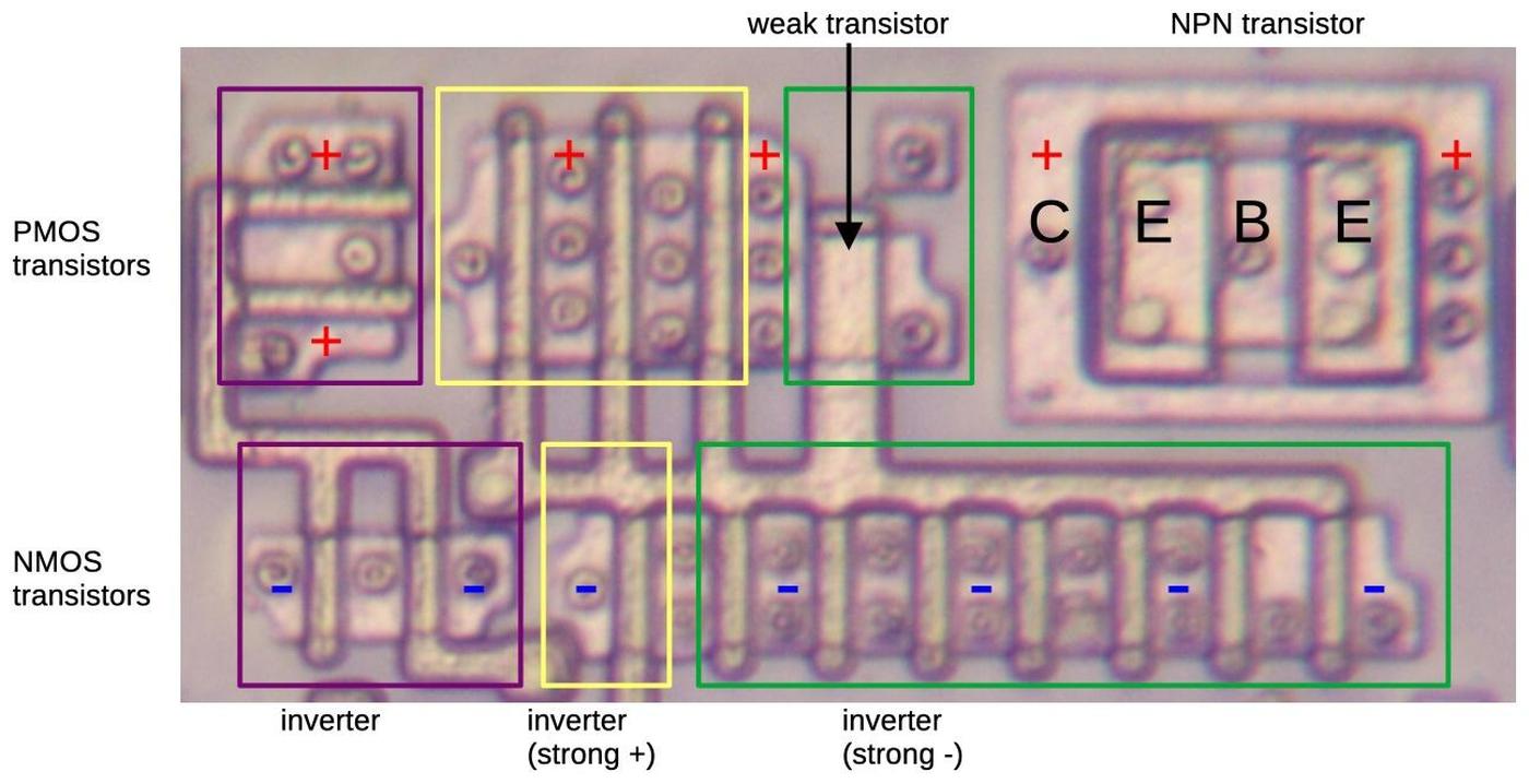
The photo below shows a closeup of two row driver circuits, next to some ROM cells.
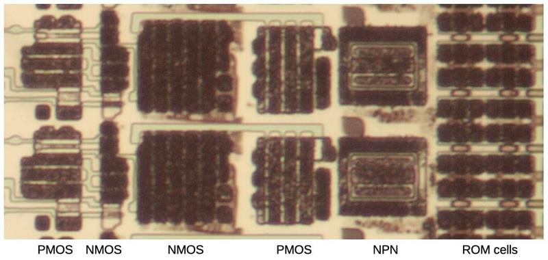
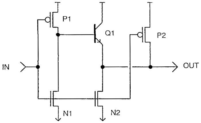
At the left, PMOS and NMOS transistors implement a gate to select the row. Next, larger NMOS and PMOS transistors form part of the driver.
The large square structures are bipolar NPN transistors; the Pentium is unusual because it uses both bipolar transistors and CMOS, a technique called BiCMOS.4
Each driver occupies as much height as four rows of the ROM, so there are four drivers arranged horizontally;
only one is visible in the photo.

ROM drivers implemented with BiCMOS.
Structure of the floating-point unit
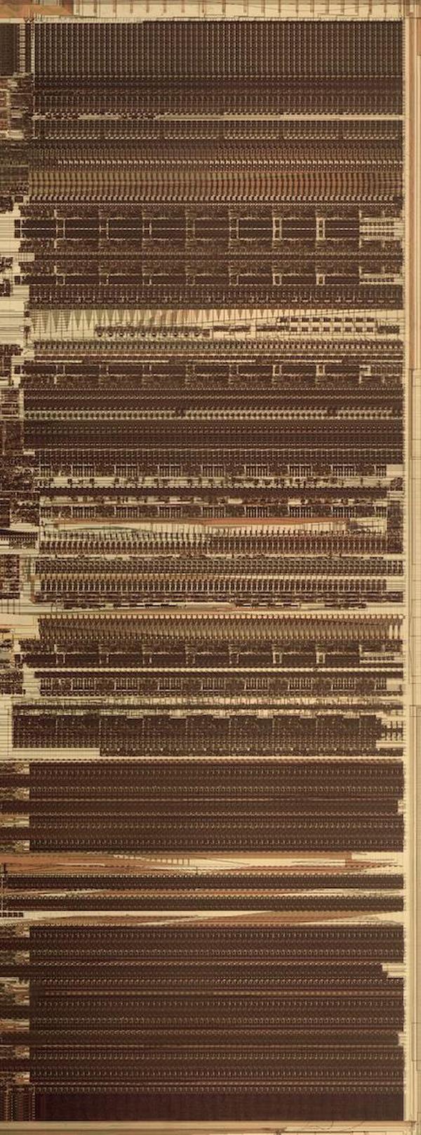
The floating-point unit is structured with data flowing vertically through horizontal functional units, as shown below.
The functional units—adders, shifters, registers, and comparators—are arranged in rows.
This collection of functional units with data flowing through them is called the datapath.5

The datapath of the floating-point unit. The ROM is at the bottom.
Each functional unit is constructed from cells, one per bit, with the high-order bit on the left and the low-order bit on the right.
Each cell has the same width—38.5 µm—so the functional units can be connected like Lego blocks snapping together, minimizing the wiring.
The height of a functional unit varies as needed, depending on the complexity of the circuit.
Functional units typically have 69 bits, but some are wider, so the edges of the datapath circuitry are ragged.
This cell-based construction explains why the ROM has eight constants per row.
A ROM bit requires a single transistor, which is much narrower than, say, an adder. Thus, putting one bit in each 38.5 µm cell would waste most of the space.
Compacting the ROM bits into a narrow block would also be inefficient, requiring diagonal wiring to connect each ROM bit to the corresponding datapath bit.
By putting eight bits for eight different constants into each cell, the width of a ROM cell matches the rest of the datapath and the alignment of bits
is preserved.
Thus, the layout of the ROM in silicon is dense, efficient, and matches the width of the rest of the floating-point unit.
Polynomial approximation: don't use a Taylor series
Now I'll move from the hardware to the constants.
If you look at the constant ROM contents in the appendix, you may notice that many constants are close to reciprocals or reciprocal factorials, but don't quite
match. For instance, one constant is 0.1111111089, which is close to 1/9, but visibly wrong.
Another constant is almost 1/13! (factorial) but wrong by 0.1%. What's going on?
The Pentium uses polynomials to approximate transcendental functions (sine, cosine, tangent, arctangent, and base-2 powers and logarithms).
Intel's earlier floating-point units, from the 8087 to the 486, used an algorithm called CORDIC that generated results
a bit at a time.
However, the Pentium takes advantage of its fast multiplier and larger ROM and uses polynomials instead,
computing results two to three times faster than the 486 algorithm.
You may recall from calculus that a Taylor series polynomial approximates a function near a point (typically 0).
For example, the equation below gives the Taylor series for sine.

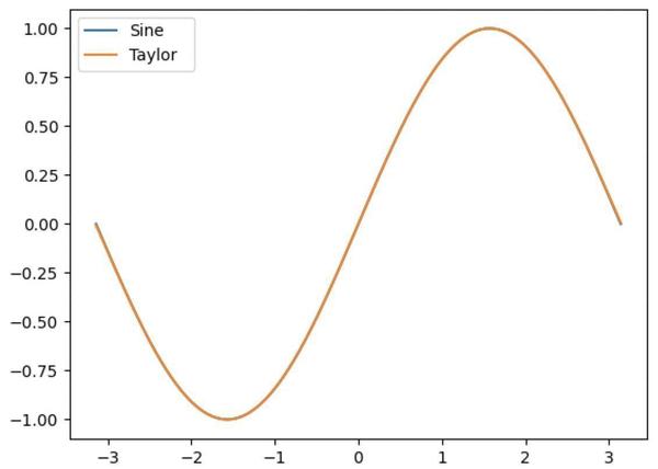
Using the five terms shown above generates a function that looks indistinguishable from sine in the graph below.
However, it turns out that this approximation has too much error to be useful.

Plot of the sine function and the Taylor series approximation.
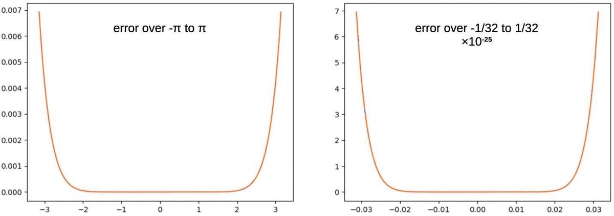
The problem is that a Taylor series is very accurate near 0, but the error soars near the edges of the argument range, as shown in the graph on the left below.
When implementing a function, we want the function to be accurate everywhere, not just close to 0, so the Taylor
series isn't good enough.

The absolute error for a Taylor-series approximation to sine (5 terms), over two different argument ranges.
One improvement is called range reduction: shrinking the argument to a smaller range so you're in the accurate flat part.6
The graph on the right looks at the Taylor series over the smaller range [-1/32, 1/32].
This decreases the error dramatically, by about 22 orders of magnitude (note the scale change).
However, the error still shoots up at the edges of the range in exactly the same way.
No matter how much
you reduce the range, there is almost no error in the middle, but the edges have a lot of error.7
How can we get rid of the error near the edges? The trick is to tweak the coefficients of the Taylor series in a special way that
will increase the error in the middle, but decrease the error at the edges by much more.
Since we want to minimize the maximum error across the range (called minimax), this tradeoff is beneficial.
Specifically, the coefficients can be optimized by a process called the Remez algorithm.8
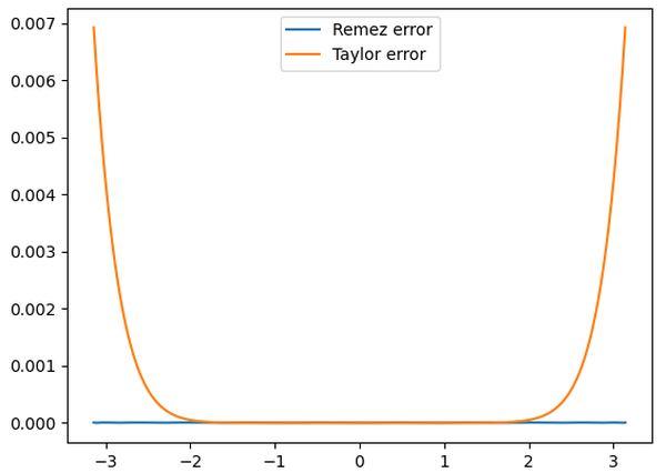
As shown below, changing the coefficients by less than 1% dramatically improves the accuracy.
The optimized function (blue) has much lower error over the full range, so it is a much better approximation than the Taylor series (orange).

Comparison of the absolute error from the Taylor series and a Remez-optimized polynomial, both with maximum term x9. This Remez polynomial is not one from the Pentium.
To summarize, a Taylor series is useful in calculus, but shouldn't be used to approximate a function. You get
a much better approximation by modifying the coefficients very slightly with the Remez algorithm. This explains
why the coefficients in the ROM almost, but not quite, match a Taylor series.
Arctan
I'll now look at the Pentium's constants for different transcendental functions.
The constant ROM contains coefficients for two arctan polynomials, one for single precision and one
for double precision.
These polynomials almost match the Taylor series, but have been modified for accuracy.
The ROM also holds the values for arctan(1/32) through arctan(32/32); the
range reduction process uses these constants with a trig identity to reduce the argument range to
[-1/64, 1/64].9
You can see the arctan constants in the Appendix.
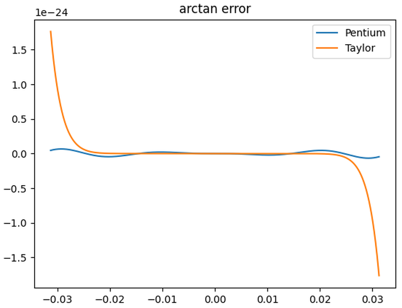
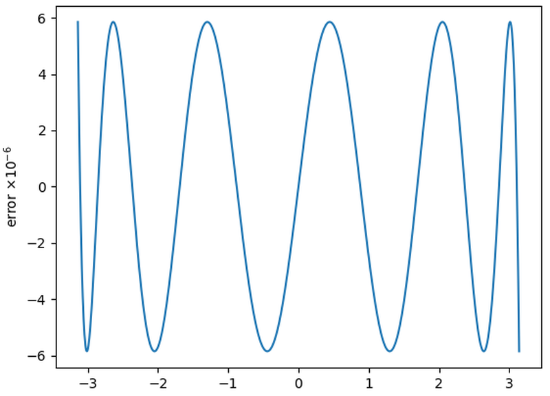
The graph below shows the error for the Pentium's arctan polynomial (blue) versus the Taylor series of the same length (orange).
The
Pentium's polynomial is superior due to the Remez optimization.
Although the Taylor series polynomial is much flatter in the middle, the error soars near the boundary.
The Pentium's polynomial wiggles more but it maintains a low error across the whole range.
The error in the Pentium polynomial blows up outside this range, but that doesn't matter.

Comparison of the Pentium's double-precision arctan polynomial to the Taylor series.
Trig functions
Sine and cosine each have two polynomial implementations, one with 4 terms in the ROM and one with 6 terms in
the ROM.
(Note that coefficients of 1 are not stored in the ROM.)
The constant table also holds 16 constants such as sin(36/64) and cos(18/64) that are used for argument range reduction.10
The Pentium computes tangent by dividing the sine by the cosine.
I'm not showing a graph because the Pentium's error came out worse than the Taylor series, so either I have an
error in a coefficient or I'm doing something wrong.
Exponential
The Pentium has an instruction to compute a power of two.11
There are two sets of polynomial coefficients for exponential, one with 6 terms in the ROM
and one with 11 terms in the ROM.
Curiously, the polynomials in the ROM compute ex, not 2x.
Thus, the Pentium must scale the argument by ln(2), a constant that is in the ROM.
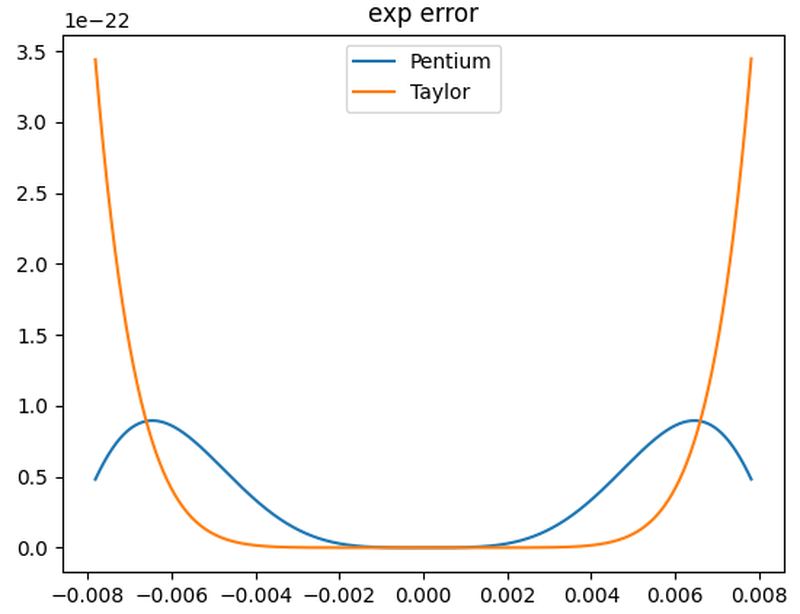
The error graph below shows the advantage of the Pentium's polynomial over the Taylor series polynomial.

The Pentium's 6-term exponential polynomial, compared with the Taylor series.
The polynomial handles the narrow argument range [-1/128, 1/128].
Observe that when computing a power of 2 in binary, exponentiating the integer part of the argument is trivial, since it becomes the result's exponent.
Thus, the function only needs to handle the range [1, 2].
For range reduction, the constant ROM holds 64 values of the form 2n/128-1.
To reduce the range from [1, 2] to [-1/128, 1/128], the closest n/128 is subtracted from the argument and then the result is multiplied by the corresponding constant in the ROM.
The constants are spaced irregularly, presumably for accuracy; some are in steps of 4/128 and others are in steps of 2/128.
Logarithm
The Pentium can compute base-2 logarithms.12
The coefficients define polynomials for the hyperbolic arctan, which is closely related to log. See the comments for details.
The ROM also has 64 constants for range reduction: log2(1+n/64) for odd n from 1 to 63.
The unusual feature of these constants is that each constant is split into two pieces to increase the bits of accuracy:
the top part has 40 bits of accuracy and the bottom part has 67 bits of accuracy, providing a 107-bit constant
in total.
The extra bits are required because logarithms are hard to compute accurately.
Other constants
The x87 floating-point instruction set provides direct access to a handful of constants—0, 1, pi,
log2(10), log2(e), log10(2), and loge(2)—so these constants
are stored in the ROM.
(These logs are useful for changing the base for logs and exponentials.)
The ROM holds other constants for internal use by the floating-point unit such as -1, 2, 7/8, 9/8, pi/2, pi/4, and 2log2(e).
The ROM also holds bitmasks for extracting part of a word, for instance accessing 4-bit BCD digits in a word.
Although I can interpret most of the values, there are a few mysteries such as a mask with the inscrutable value
0x3e8287c.
The ROM has 34 unused entries at the end; these entries hold words that include the descriptive hex value 0xbad or perhaps 0xbadfc for "bad float constant".
How I examined the ROM
To analyze the Pentium, I removed the metal and oxide layers with various chemicals (sulfuric acid, phosphoric acid, Whink).
(I later discovered that simply sanding the die works surprisingly well.)
Next, I took many photos of the ROM with a microscope.
The feature size of this Pentium is 800 nm, just slightly larger than visible light (380-700 nm).
Thus, the die can be examined under an optical microscope, but it is getting close to the limits.
To determine the ROM contents, I tediously went through the ROM images, examining each of the 26144 bits and marking each transistor.
After figuring out the ROM format,
I wrote programs to combine simple functions in many different combinations to
determine the mathematical expression such as arctan(19/32) or log2(10).
Because the polynomial constants are optimized and my ROM data has bit errors, my program needed
checks for inexact matches, both numerically and bitwise.
Finally, I had to determine how the constants would be used in algorithms.
Conclusions
By examining the Pentium's floating-point ROM under a microscope, it is possible to extract the 304 constants
stored in the ROM.
I was able to determine the meaning of most of these constants and deduce some of the floating-point algorithms used
by the Pentium.
These constants illustrate how polynomials can efficiently compute transcendental functions.
Although Taylor series polynomials are well known, they are surprisingly inaccurate and should be avoided.
Minor changes to the coefficients through the Remez algorithm, however, yield much better polynomials.
In a previous article, I examined the floating-point constants stored in the 8087 coprocessor.
The Pentium has 304 constants in the Pentium, compared to just 42 in the 8087, supporting more efficient algorithms.
Moreover, the 8087 was an external floating-point unit, while the Pentium's floating-point unit is part of the
processor.
The changes between the 8087 (1980, 65,000 transistors) and the Pentium (1993, 3.1 million transistors) are due
to the exponential improvements in transistor count, as described by Moore's Law.
I plan to write more about the Pentium so follow me on Bluesky (@righto.com) or
RSS for updates. (I'm no longer on Twitter.)
I've also written about the Pentium division bug and the Pentium Navajo rug.
Thanks to CuriousMarc for microscope help. Thanks to lifthrasiir and Alexia for identifying some constants.
Appendix: The constant ROM
The table below lists the 304 constants in the Pentium's floating-point ROM.
The first four columns show the values stored in the ROM: the exponent, the sign bit, the flag bit, and the
significand.
To avoid negative exponents, exponents are stored with the constant 0x0ffff added. For example, the value 0x0fffe
represents an exponent of -1, while 0x10000 represents an exponent of 1.
The constant's approximate decimal value is in the "value" column.
Special-purpose values are colored. Specifically, "normal" numbers are in black.
Constants with an exponent of all 0's are in blue,
constants with an exponent of all 1's are in red,
constants with an unusually large or small exponent are in green;
these appear to be bitmasks rather than numbers.
Unused entries are in gray.
Inexact constants (due to Remez optimization) are represented with the approximation symbol "≈".
This information is from my reverse engineering, so there will be a few errors.
| exp | S | F | significand | value | meaning |
|---|
| 0 |
00000 |
0 |
0 |
07878787878787878 |
|
BCD mask by 4's |
| 1 |
00000 |
0 |
0 |
007f807f807f807f8 |
|
BCD mask by 8's |
| 2 |
00000 |
0 |
0 |
00007fff80007fff8 |
|
BCD mask by 16's |
| 3 |
00000 |
0 |
0 |
000000007fffffff8 |
|
BCD mask by 32's |
| 4 |
00000 |
0 |
0 |
78000000000000000 |
|
4-bit mask |
| 5 |
00000 |
0 |
0 |
18000000000000000 |
|
2-bit mask |
| 6 |
00000 |
0 |
0 |
27000000000000000 |
|
? |
| 7 |
00000 |
0 |
0 |
363c0000000000000 |
|
? |
| 8 |
00000 |
0 |
0 |
3e8287c0000000000 |
|
? |
| 9 |
00000 |
0 |
0 |
470de4df820000000 |
|
213×1016 |
| 10 |
00000 |
0 |
0 |
5c3bd5191b525a249 |
|
2123/1017 |
| 11 |
00000 |
0 |
0 |
00000000000000007 |
|
3-bit mask |
| 12 |
1ffff |
1 |
1 |
7ffffffffffffffff |
|
all 1's |
| 13 |
00000 |
0 |
0 |
0000007ffffffffff |
|
mask for 32-bit float |
| 14 |
00000 |
0 |
0 |
00000000000003fff |
|
mask for 64-bit float |
| 15 |
00000 |
0 |
0 |
00000000000000000 |
|
all 0's |
| 16 |
0ffff |
0 |
0 |
40000000000000000 |
1 |
1 |
| 17 |
10000 |
0 |
0 |
6a4d3c25e68dc57f2 |
3.3219280949 |
log2(10) |
| 18 |
0ffff |
0 |
0 |
5c551d94ae0bf85de |
1.4426950409 |
log2(e) |
| 19 |
10000 |
0 |
0 |
6487ed5110b4611a6 |
3.1415926536 |
pi |
| 20 |
0ffff |
0 |
0 |
6487ed5110b4611a6 |
1.5707963268 |
pi/2 |
| 21 |
0fffe |
0 |
0 |
6487ed5110b4611a6 |
0.7853981634 |
pi/4 |
| 22 |
0fffd |
0 |
0 |
4d104d427de7fbcc5 |
0.3010299957 |
log10(2) |
| 23 |
0fffe |
0 |
0 |
58b90bfbe8e7bcd5f |
0.6931471806 |
ln(2) |
| 24 |
1ffff |
0 |
0 |
40000000000000000 |
|
+infinity |
| 25 |
0bfc0 |
0 |
0 |
40000000000000000 |
|
1/4 of smallest 80-bit denormal? |
| 26 |
1ffff |
1 |
0 |
60000000000000000 |
|
NaN (not a number) |
| 27 |
0ffff |
1 |
0 |
40000000000000000 |
-1 |
-1 |
| 28 |
10000 |
0 |
0 |
40000000000000000 |
2 |
2 |
| 29 |
00000 |
0 |
0 |
00000000000000001 |
|
low bit |
| 30 |
00000 |
0 |
0 |
00000000000000000 |
|
all 0's |
| 31 |
00001 |
0 |
0 |
00000000000000000 |
|
single exponent bit |
| 32 |
0fffe |
0 |
0 |
58b90bfbe8e7bcd5e |
0.6931471806 |
ln(2) |
| 33 |
0fffe |
0 |
0 |
40000000000000000 |
0.5 |
1/2! (exp Taylor series) |
| 34 |
0fffc |
0 |
0 |
5555555555555584f |
0.1666666667 |
≈1/3! |
| 35 |
0fffa |
0 |
0 |
555555555397fffd4 |
0.0416666667 |
≈1/4! |
| 36 |
0fff8 |
0 |
0 |
444444444250ced0c |
0.0083333333 |
≈1/5! |
| 37 |
0fff5 |
0 |
0 |
5b05c3dd3901cea50 |
0.0013888934 |
≈1/6! |
| 38 |
0fff2 |
0 |
0 |
6806988938f4f2318 |
0.0001984134 |
≈1/7! |
| 39 |
0fffe |
0 |
0 |
40000000000000000 |
0.5 |
1/2! (exp Taylor series) |
| 40 |
0fffc |
0 |
0 |
5555555555555558e |
0.1666666667 |
≈1/3! |
| 41 |
0fffa |
0 |
0 |
5555555555555558b |
0.0416666667 |
≈1/4! |
| 42 |
0fff8 |
0 |
0 |
444444444443db621 |
0.0083333333 |
≈1/5! |
| 43 |
0fff5 |
0 |
0 |
5b05b05b05afd42f4 |
0.0013888889 |
≈1/6! |
| 44 |
0fff2 |
0 |
0 |
68068068163b44194 |
0.0001984127 |
≈1/7! |
| 45 |
0ffef |
0 |
0 |
6806806815d1b6d8a |
0.0000248016 |
≈1/8! |
| 46 |
0ffec |
0 |
0 |
5c778d8e0384c73ab |
2.755731e-06 |
≈1/9! |
| 47 |
0ffe9 |
0 |
0 |
49f93e0ef41d6086b |
2.755731e-07 |
≈1/10! |
| 48 |
0ffe5 |
0 |
0 |
6ba8b65b40f9c0ce8 |
2.506632e-08 |
≈1/11! |
| 49 |
0ffe2 |
0 |
0 |
47c5b695d0d1289a8 |
2.088849e-09 |
≈1/12! |
| 50 |
0fffd |
0 |
0 |
6dfb23c651a2ef221 |
0.4296133384 |
266/128-1 |
| 51 |
0fffd |
0 |
0 |
75feb564267c8bf6f |
0.4609177942 |
270/128-1 |
| 52 |
0fffd |
0 |
0 |
7e2f336cf4e62105d |
0.4929077283 |
274/128-1 |
| 53 |
0fffe |
0 |
0 |
4346ccda249764072 |
0.5255981507 |
278/128-1 |
| 54 |
0fffe |
0 |
0 |
478d74c8abb9b15cc |
0.5590044002 |
282/128-1 |
| 55 |
0fffe |
0 |
0 |
4bec14fef2727c5cf |
0.5931421513 |
286/128-1 |
| 56 |
0fffe |
0 |
0 |
506333daef2b2594d |
0.6280274219 |
290/128-1 |
| 57 |
0fffe |
0 |
0 |
54f35aabcfedfa1f6 |
0.6636765803 |
294/128-1 |
| 58 |
0fffe |
0 |
0 |
599d15c278afd7b60 |
0.7001063537 |
298/128-1 |
| 59 |
0fffe |
0 |
0 |
5e60f4825e0e9123e |
0.7373338353 |
2102/128-1 |
| 60 |
0fffe |
0 |
0 |
633f8972be8a5a511 |
0.7753764925 |
2106/128-1 |
| 61 |
0fffe |
0 |
0 |
68396a503c4bdc688 |
0.8142521755 |
2110/128-1 |
| 62 |
0fffe |
0 |
0 |
6d4f301ed9942b846 |
0.8539791251 |
2114/128-1 |
| 63 |
0fffe |
0 |
0 |
7281773c59ffb139f |
0.8945759816 |
2118/128-1 |
| 64 |
0fffe |
0 |
0 |
77d0df730ad13bb90 |
0.9360617935 |
2122/128-1 |
| 65 |
0fffe |
0 |
0 |
7d3e0c0cf486c1748 |
0.9784560264 |
2126/128-1 |
| 66 |
0fffc |
0 |
0 |
642e1f899b0626a74 |
0.1956643920 |
233/128-1 |
| 67 |
0fffc |
0 |
0 |
6ad8abf253fe1928c |
0.2086843236 |
235/128-1 |
| 68 |
0fffc |
0 |
0 |
7195cda0bb0cb0b54 |
0.2218460330 |
237/128-1 |
| 69 |
0fffc |
0 |
0 |
7865b862751c90800 |
0.2351510639 |
239/128-1 |
| 70 |
0fffc |
0 |
0 |
7f48a09590037417f |
0.2486009772 |
241/128-1 |
| 71 |
0fffd |
0 |
0 |
431f5d950a896dc70 |
0.2621973504 |
243/128-1 |
| 72 |
0fffd |
0 |
0 |
46a41ed1d00577251 |
0.2759417784 |
245/128-1 |
| 73 |
0fffd |
0 |
0 |
4a32af0d7d3de672e |
0.2898358734 |
247/128-1 |
| 74 |
0fffd |
0 |
0 |
4dcb299fddd0d63b3 |
0.3038812652 |
249/128-1 |
| 75 |
0fffd |
0 |
0 |
516daa2cf6641c113 |
0.3180796013 |
251/128-1 |
| 76 |
0fffd |
0 |
0 |
551a4ca5d920ec52f |
0.3324325471 |
253/128-1 |
| 77 |
0fffd |
0 |
0 |
58d12d497c7fd252c |
0.3469417862 |
255/128-1 |
| 78 |
0fffd |
0 |
0 |
5c9268a5946b701c5 |
0.3616090206 |
257/128-1 |
| 79 |
0fffd |
0 |
0 |
605e1b976dc08b077 |
0.3764359708 |
259/128-1 |
| 80 |
0fffd |
0 |
0 |
6434634ccc31fc770 |
0.3914243758 |
261/128-1 |
| 81 |
0fffd |
0 |
0 |
68155d44ca973081c |
0.4065759938 |
263/128-1 |
| 82 |
0fffd |
1 |
0 |
4cee3bed56eedb76c |
-0.3005101637 |
2-66/128-1 |
| 83 |
0fffd |
1 |
0 |
50c4875296f5bc8b2 |
-0.3154987885 |
2-70/128-1 |
| 84 |
0fffd |
1 |
0 |
5485c64a56c12cc8a |
-0.3301662380 |
2-74/128-1 |
| 85 |
0fffd |
1 |
0 |
58326c4b169aca966 |
-0.3445193942 |
2-78/128-1 |
| 86 |
0fffd |
1 |
0 |
5bcaea51f6197f61f |
-0.3585649920 |
2-82/128-1 |
| 87 |
0fffd |
1 |
0 |
5f4faef0468eb03de |
-0.3723096215 |
2-86/128-1 |
| 88 |
0fffd |
1 |
0 |
62c12658d30048af2 |
-0.3857597319 |
2-90/128-1 |
| 89 |
0fffd |
1 |
0 |
661fba6cdf48059b2 |
-0.3989216343 |
2-94/128-1 |
| 90 |
0fffd |
1 |
0 |
696bd2c8dfe7a5ffb |
-0.4118015042 |
2-98/128-1 |
| 91 |
0fffd |
1 |
0 |
6ca5d4d0ec1916d43 |
-0.4244053850 |
2-102/128-1 |
| 92 |
0fffd |
1 |
0 |
6fce23bceb994e239 |
-0.4367391907 |
2-106/128-1 |
| 93 |
0fffd |
1 |
0 |
72e520a481a4561a5 |
-0.4488087083 |
2-110/128-1 |
| 94 |
0fffd |
1 |
0 |
75eb2a8ab6910265f |
-0.4606196011 |
2-114/128-1 |
| 95 |
0fffd |
1 |
0 |
78e09e696172efefc |
-0.4721774108 |
2-118/128-1 |
| 96 |
0fffd |
1 |
0 |
7bc5d73c5321bfb9e |
-0.4834875605 |
2-122/128-1 |
| 97 |
0fffd |
1 |
0 |
7e9b2e0c43fcf88c8 |
-0.4945553570 |
2-126/128-1 |
| 98 |
0fffc |
1 |
0 |
53c94402c0c863f24 |
-0.1636449102 |
2-33/128-1 |
| 99 |
0fffc |
1 |
0 |
58661eccf4ca790d2 |
-0.1726541162 |
2-35/128-1 |
| 100 |
0fffc |
1 |
0 |
5cf6413b5d2cca73f |
-0.1815662751 |
2-37/128-1 |
| 101 |
0fffc |
1 |
0 |
6179ce61cdcdce7db |
-0.1903824324 |
2-39/128-1 |
| 102 |
0fffc |
1 |
0 |
65f0e8f35f84645cf |
-0.1991036222 |
2-41/128-1 |
| 103 |
0fffc |
1 |
0 |
6a5bb3437adf1164b |
-0.2077308674 |
2-43/128-1 |
| 104 |
0fffc |
1 |
0 |
6eba4f46e003a775a |
-0.2162651800 |
2-45/128-1 |
| 105 |
0fffc |
1 |
0 |
730cde94abb7410d5 |
-0.2247075612 |
2-47/128-1 |
| 106 |
0fffc |
1 |
0 |
775382675996699ad |
-0.2330590011 |
2-49/128-1 |
| 107 |
0fffc |
1 |
0 |
7b8e5b9dc385331ad |
-0.2413204794 |
2-51/128-1 |
| 108 |
0fffc |
1 |
0 |
7fbd8abc1e5ee49f2 |
-0.2494929652 |
2-53/128-1 |
| 109 |
0fffd |
1 |
0 |
41f097f679f66c1db |
-0.2575774171 |
2-55/128-1 |
| 110 |
0fffd |
1 |
0 |
43fcb5810d1604f37 |
-0.2655747833 |
2-57/128-1 |
| 111 |
0fffd |
1 |
0 |
46032dbad3f462152 |
-0.2734860021 |
2-59/128-1 |
| 112 |
0fffd |
1 |
0 |
48041035735be183c |
-0.2813120013 |
2-61/128-1 |
| 113 |
0fffd |
1 |
0 |
49ff6c57a12a08945 |
-0.2890536989 |
2-63/128-1 |
| 114 |
0fffd |
1 |
0 |
555555555555535f0 |
-0.3333333333 |
≈-1/3 (arctan Taylor series) |
| 115 |
0fffc |
0 |
0 |
6666666664208b016 |
0.2 |
≈ 1/5 |
| 116 |
0fffc |
1 |
0 |
492491e0653ac37b8 |
-0.1428571307 |
≈-1/7 |
| 117 |
0fffb |
0 |
0 |
71b83f4133889b2f0 |
0.1110544094 |
≈ 1/9 |
| 118 |
0fffd |
1 |
0 |
55555555555555543 |
-0.3333333333 |
≈-1/3 (arctan Taylor series) |
| 119 |
0fffc |
0 |
0 |
66666666666616b73 |
0.2 |
≈ 1/5 |
| 120 |
0fffc |
1 |
0 |
4924924920fca4493 |
-0.1428571429 |
≈-1/7 |
| 121 |
0fffb |
0 |
0 |
71c71c4be6f662c91 |
0.1111111089 |
≈ 1/9 |
| 122 |
0fffb |
1 |
0 |
5d16e0bde0b12eee8 |
-0.0909075848 |
≈-1/11 |
| 123 |
0fffb |
0 |
0 |
4e403be3e3c725aa0 |
0.0764169081 |
≈ 1/13 |
| 124 |
00000 |
0 |
0 |
40000000000000000 |
|
single bit mask |
| 125 |
0fff9 |
0 |
0 |
7ff556eea5d892a14 |
0.0312398334 |
arctan(1/32) |
| 126 |
0fffa |
0 |
0 |
7fd56edcb3f7a71b6 |
0.0624188100 |
arctan(2/32) |
| 127 |
0fffb |
0 |
0 |
5fb860980bc43a305 |
0.0934767812 |
arctan(3/32) |
| 128 |
0fffb |
0 |
0 |
7f56ea6ab0bdb7196 |
0.1243549945 |
arctan(4/32) |
| 129 |
0fffc |
0 |
0 |
4f5bbba31989b161a |
0.1549967419 |
arctan(5/32) |
| 130 |
0fffc |
0 |
0 |
5ee5ed2f396c089a4 |
0.1853479500 |
arctan(6/32) |
| 131 |
0fffc |
0 |
0 |
6e435d4a498288118 |
0.2153576997 |
arctan(7/32) |
| 132 |
0fffc |
0 |
0 |
7d6dd7e4b203758ab |
0.2449786631 |
arctan(8/32) |
| 133 |
0fffd |
0 |
0 |
462fd68c2fc5e0986 |
0.2741674511 |
arctan(9/32) |
| 134 |
0fffd |
0 |
0 |
4d89dcdc1faf2f34e |
0.3028848684 |
arctan(10/32) |
| 135 |
0fffd |
0 |
0 |
54c2b6654735276d5 |
0.3310960767 |
arctan(11/32) |
| 136 |
0fffd |
0 |
0 |
5bd86507937bc239c |
0.3587706703 |
arctan(12/32) |
| 137 |
0fffd |
0 |
0 |
62c934e5286c95b6d |
0.3858826694 |
arctan(13/32) |
| 138 |
0fffd |
0 |
0 |
6993bb0f308ff2db2 |
0.4124104416 |
arctan(14/32) |
| 139 |
0fffd |
0 |
0 |
7036d3253b27be33e |
0.4383365599 |
arctan(15/32) |
| 140 |
0fffd |
0 |
0 |
76b19c1586ed3da2b |
0.4636476090 |
arctan(16/32) |
| 141 |
0fffd |
0 |
0 |
7d03742d50505f2e3 |
0.4883339511 |
arctan(17/32) |
| 142 |
0fffe |
0 |
0 |
4195fa536cc33f152 |
0.5123894603 |
arctan(18/32) |
| 143 |
0fffe |
0 |
0 |
4495766fef4aa3da8 |
0.5358112380 |
arctan(19/32) |
| 144 |
0fffe |
0 |
0 |
47802eaf7bfacfcdb |
0.5585993153 |
arctan(20/32) |
| 145 |
0fffe |
0 |
0 |
4a563964c238c37b1 |
0.5807563536 |
arctan(21/32) |
| 146 |
0fffe |
0 |
0 |
4d17c07338deed102 |
0.6022873461 |
arctan(22/32) |
| 147 |
0fffe |
0 |
0 |
4fc4fee27a5bd0f68 |
0.6231993299 |
arctan(23/32) |
| 148 |
0fffe |
0 |
0 |
525e3e8c9a7b84921 |
0.6435011088 |
arctan(24/32) |
| 149 |
0fffe |
0 |
0 |
54e3d5ee24187ae45 |
0.6632029927 |
arctan(25/32) |
| 150 |
0fffe |
0 |
0 |
5756261c5a6c60401 |
0.6823165549 |
arctan(26/32) |
| 151 |
0fffe |
0 |
0 |
59b598e48f821b48b |
0.7008544079 |
arctan(27/32) |
| 152 |
0fffe |
0 |
0 |
5c029f15e118cf39e |
0.7188299996 |
arctan(28/32) |
| 153 |
0fffe |
0 |
0 |
5e3daef574c579407 |
0.7362574290 |
arctan(29/32) |
| 154 |
0fffe |
0 |
0 |
606742dc562933204 |
0.7531512810 |
arctan(30/32) |
| 155 |
0fffe |
0 |
0 |
627fd7fd5fc7deaa4 |
0.7695264804 |
arctan(31/32) |
| 156 |
0fffe |
0 |
0 |
6487ed5110b4611a6 |
0.7853981634 |
arctan(32/32) |
| 157 |
0fffc |
1 |
0 |
55555555555555555 |
-0.1666666667 |
≈-1/3! (sin Taylor series) |
| 158 |
0fff8 |
0 |
0 |
44444444444443e35 |
0.0083333333 |
≈ 1/5! |
| 159 |
0fff2 |
1 |
0 |
6806806806773c774 |
-0.0001984127 |
≈-1/7! |
| 160 |
0ffec |
0 |
0 |
5c778e94f50956d70 |
2.755732e-06 |
≈ 1/9! |
| 161 |
0ffe5 |
1 |
0 |
6b991122efa0532f0 |
-2.505209e-08 |
≈-1/11! |
| 162 |
0ffde |
0 |
0 |
58303f02614d5e4d8 |
1.604139e-10 |
≈ 1/13! |
| 163 |
0fffd |
1 |
0 |
7fffffffffffffffe |
-0.5 |
≈-1/2! (cos Taylor series) |
| 164 |
0fffa |
0 |
0 |
55555555555554277 |
0.0416666667 |
≈ 1/4! |
| 165 |
0fff5 |
1 |
0 |
5b05b05b05a18a1ba |
-0.0013888889 |
≈-1/6! |
| 166 |
0ffef |
0 |
0 |
680680675b559f2cf |
0.0000248016 |
≈ 1/8! |
| 167 |
0ffe9 |
1 |
0 |
49f93af61f5349300 |
-2.755730e-07 |
≈-1/10! |
| 168 |
0ffe2 |
0 |
0 |
47a4f2483514c1af8 |
2.085124e-09 |
≈ 1/12! |
| 169 |
0fffc |
1 |
0 |
55555555555555445 |
-0.1666666667 |
≈-1/3! (sin Taylor series) |
| 170 |
0fff8 |
0 |
0 |
44444444443a3fdb6 |
0.0083333333 |
≈ 1/5! |
| 171 |
0fff2 |
1 |
0 |
68068060b2044e9ae |
-0.0001984127 |
≈-1/7! |
| 172 |
0ffec |
0 |
0 |
5d75716e60f321240 |
2.785288e-06 |
≈ 1/9! |
| 173 |
0fffd |
1 |
0 |
7fffffffffffffa28 |
-0.5 |
≈-1/2! (cos Taylor series) |
| 174 |
0fffa |
0 |
0 |
555555555539cfae6 |
0.0416666667 |
≈ 1/4! |
| 175 |
0fff5 |
1 |
0 |
5b05b050f31b2e713 |
-0.0013888889 |
≈-1/6! |
| 176 |
0ffef |
0 |
0 |
6803988d56e3bff10 |
0.0000247989 |
≈ 1/8! |
| 177 |
0fffe |
0 |
0 |
44434312da70edd92 |
0.5333026735 |
sin(36/64) |
| 178 |
0fffe |
0 |
0 |
513ace073ce1aac13 |
0.6346070800 |
sin(44/64) |
| 179 |
0fffe |
0 |
0 |
5cedda037a95df6ee |
0.7260086553 |
sin(52/64) |
| 180 |
0fffe |
0 |
0 |
672daa6ef3992b586 |
0.8060811083 |
sin(60/64) |
| 181 |
0fffd |
0 |
0 |
470df5931ae1d9460 |
0.2775567516 |
sin(18/64) |
| 182 |
0fffd |
0 |
0 |
5646f27e8bd65cbe4 |
0.3370200690 |
sin(22/64) |
| 183 |
0fffd |
0 |
0 |
6529afa7d51b12963 |
0.3951673302 |
sin(26/64) |
| 184 |
0fffd |
0 |
0 |
73a74b8f52947b682 |
0.4517714715 |
sin(30/64) |
| 185 |
0fffe |
0 |
0 |
6c4741058a93188ef |
0.8459244992 |
cos(36/64) |
| 186 |
0fffe |
0 |
0 |
62ec41e9772401864 |
0.7728350058 |
cos(44/64) |
| 187 |
0fffe |
0 |
0 |
5806149bd58f7d46d |
0.6876855622 |
cos(52/64) |
| 188 |
0fffe |
0 |
0 |
4bc044c9908390c72 |
0.5918050751 |
cos(60/64) |
| 189 |
0fffe |
0 |
0 |
7af8853ddbbe9ffd0 |
0.9607092430 |
cos(18/64) |
| 190 |
0fffe |
0 |
0 |
7882fd26b35b03d34 |
0.9414974631 |
cos(22/64) |
| 191 |
0fffe |
0 |
0 |
7594fc1cf900fe89e |
0.9186091558 |
cos(26/64) |
| 192 |
0fffe |
0 |
0 |
72316fe3386a10d5a |
0.8921336994 |
cos(30/64) |
| 193 |
0ffff |
0 |
0 |
48000000000000000 |
1.125 |
9/8 |
| 194 |
0fffe |
0 |
0 |
70000000000000000 |
0.875 |
7/8 |
| 195 |
0ffff |
0 |
0 |
5c551d94ae0bf85de |
1.4426950409 |
log2(e) |
| 196 |
10000 |
0 |
0 |
5c551d94ae0bf85de |
2.8853900818 |
2log2(e) |
| 197 |
0fffb |
0 |
0 |
7b1c2770e81287c11 |
0.1202245867 |
≈1/(41⋅3⋅ln(2)) (atanh series for log) |
| 198 |
0fff9 |
0 |
0 |
49ddb14064a5d30bd |
0.0180336880 |
≈1/(42⋅5⋅ln(2)) |
| 199 |
0fff6 |
0 |
0 |
698879b87934f12e0 |
0.0032206148 |
≈1/(43⋅7⋅ln(2)) |
| 200 |
0fffa |
0 |
0 |
51ff4ffeb20ed1749 |
0.0400377512 |
≈(ln(2)/2)2/3 (atanh series for log) |
| 201 |
0fff6 |
0 |
0 |
5e8cd07eb1827434a |
0.0028854387 |
≈(ln(2)/2)4/5 |
| 202 |
0fff3 |
0 |
0 |
40e54061b26dd6dc2 |
0.0002475567 |
≈(ln(2)/2)6/7 |
| 203 |
0ffef |
0 |
0 |
61008a69627c92fb9 |
0.0000231271 |
≈(ln(2)/2)8/9 |
| 204 |
0ffec |
0 |
0 |
4c41e6ced287a2468 |
2.272648e-06 |
≈(ln(2)/2)10/11 |
| 205 |
0ffe8 |
0 |
0 |
7dadd4ea3c3fee620 |
2.340954e-07 |
≈(ln(2)/2)12/13 |
| 206 |
0fff9 |
0 |
0 |
5b9e5a170b8000000 |
0.0223678130 |
log2(1+1/64) top bits |
| 207 |
0fffb |
0 |
0 |
43ace37e8a8000000 |
0.0660892054 |
log2(1+3/64) top bits |
| 208 |
0fffb |
0 |
0 |
6f210902b68000000 |
0.1085244568 |
log2(1+5/64) top bits |
| 209 |
0fffc |
0 |
0 |
4caba789e28000000 |
0.1497471195 |
log2(1+7/64) top bits |
| 210 |
0fffc |
0 |
0 |
6130af40bc0000000 |
0.1898245589 |
log2(1+9/64) top bits |
| 211 |
0fffc |
0 |
0 |
7527b930c98000000 |
0.2288186905 |
log2(1+11/64) top bits |
| 212 |
0fffd |
0 |
0 |
444c1f6b4c0000000 |
0.2667865407 |
log2(1+13/64) top bits |
| 213 |
0fffd |
0 |
0 |
4dc4933a930000000 |
0.3037807482 |
log2(1+15/64) top bits |
| 214 |
0fffd |
0 |
0 |
570068e7ef8000000 |
0.3398500029 |
log2(1+17/64) top bits |
| 215 |
0fffd |
0 |
0 |
6002958c588000000 |
0.3750394313 |
log2(1+19/64) top bits |
| 216 |
0fffd |
0 |
0 |
68cdd829fd8000000 |
0.4093909361 |
log2(1+21/64) top bits |
| 217 |
0fffd |
0 |
0 |
7164beb4a58000000 |
0.4429434958 |
log2(1+23/64) top bits |
| 218 |
0fffd |
0 |
0 |
79c9aa879d8000000 |
0.4757334310 |
log2(1+25/64) top bits |
| 219 |
0fffe |
0 |
0 |
40ff6a2e5e8000000 |
0.5077946402 |
log2(1+27/64) top bits |
| 220 |
0fffe |
0 |
0 |
450327ea878000000 |
0.5391588111 |
log2(1+29/64) top bits |
| 221 |
0fffe |
0 |
0 |
48f107509c8000000 |
0.5698556083 |
log2(1+31/64) top bits |
| 222 |
0fffe |
0 |
0 |
4cc9f1aad28000000 |
0.5999128422 |
log2(1+33/64) top bits |
| 223 |
0fffe |
0 |
0 |
508ec1fa618000000 |
0.6293566201 |
log2(1+35/64) top bits |
| 224 |
0fffe |
0 |
0 |
5440461c228000000 |
0.6582114828 |
log2(1+37/64) top bits |
| 225 |
0fffe |
0 |
0 |
57df3fd0780000000 |
0.6865005272 |
log2(1+39/64) top bits |
| 226 |
0fffe |
0 |
0 |
5b6c65a9d88000000 |
0.7142455177 |
log2(1+41/64) top bits |
| 227 |
0fffe |
0 |
0 |
5ee863e4d40000000 |
0.7414669864 |
log2(1+43/64) top bits |
| 228 |
0fffe |
0 |
0 |
6253dd2c1b8000000 |
0.7681843248 |
log2(1+45/64) top bits |
| 229 |
0fffe |
0 |
0 |
65af6b4ab30000000 |
0.7944158664 |
log2(1+47/64) top bits |
| 230 |
0fffe |
0 |
0 |
68fb9fce388000000 |
0.8201789624 |
log2(1+49/64) top bits |
| 231 |
0fffe |
0 |
0 |
6c39049af30000000 |
0.8454900509 |
log2(1+51/64) top bits |
| 232 |
0fffe |
0 |
0 |
6f681c731a0000000 |
0.8703647196 |
log2(1+53/64) top bits |
| 233 |
0fffe |
0 |
0 |
72896372a50000000 |
0.8948177633 |
log2(1+55/64) top bits |
| 234 |
0fffe |
0 |
0 |
759d4f80cb8000000 |
0.9188632373 |
log2(1+57/64) top bits |
| 235 |
0fffe |
0 |
0 |
78a450b8380000000 |
0.9425145053 |
log2(1+59/64) top bits |
| 236 |
0fffe |
0 |
0 |
7b9ed1c6ce8000000 |
0.9657842847 |
log2(1+61/64) top bits |
| 237 |
0fffe |
0 |
0 |
7e8d3845df0000000 |
0.9886846868 |
log2(1+63/64) top bits |
| 238 |
0ffd0 |
1 |
0 |
6eb3ac8ec0ef73f7b |
-1.229037e-14 |
log2(1+1/64) bottom bits |
| 239 |
0ffcd |
1 |
0 |
654c308b454666de9 |
-1.405787e-15 |
log2(1+3/64) bottom bits |
| 240 |
0ffd2 |
0 |
0 |
5dd31d962d3728cbd |
4.166652e-14 |
log2(1+5/64) bottom bits |
| 241 |
0ffd3 |
0 |
0 |
70d0fa8f9603ad3a6 |
1.002010e-13 |
log2(1+7/64) bottom bits |
| 242 |
0ffd1 |
0 |
0 |
765fba4491dcec753 |
2.628429e-14 |
log2(1+9/64) bottom bits |
| 243 |
0ffd2 |
1 |
0 |
690370b4a9afdc5fb |
-4.663533e-14 |
log2(1+11/64) bottom bits |
| 244 |
0ffd4 |
0 |
0 |
5bae584b82d3cad27 |
1.628582e-13 |
log2(1+13/64) bottom bits |
| 245 |
0ffd4 |
0 |
0 |
6f66cc899b64303f7 |
1.978889e-13 |
log2(1+15/64) bottom bits |
| 246 |
0ffd4 |
1 |
0 |
4bc302ffa76fafcba |
-1.345799e-13 |
log2(1+17/64) bottom bits |
| 247 |
0ffd2 |
1 |
0 |
7579aa293ec16410a |
-5.216949e-14 |
log2(1+19/64) bottom bits |
| 248 |
0ffcf |
0 |
0 |
509d7c40d7979ec5b |
4.475041e-15 |
log2(1+21/64) bottom bits |
| 249 |
0ffd3 |
1 |
0 |
4a981811ab5110ccf |
-6.625289e-14 |
log2(1+23/64) bottom bits |
| 250 |
0ffd4 |
1 |
0 |
596f9d730f685c776 |
-1.588702e-13 |
log2(1+25/64) bottom bits |
| 251 |
0ffd4 |
1 |
0 |
680cc6bcb9bfa9853 |
-1.848298e-13 |
log2(1+27/64) bottom bits |
| 252 |
0ffd4 |
0 |
0 |
5439e15a52a31604a |
1.496156e-13 |
log2(1+29/64) bottom bits |
| 253 |
0ffd4 |
0 |
0 |
7c8080ecc61a98814 |
2.211599e-13 |
log2(1+31/64) bottom bits |
| 254 |
0ffd3 |
1 |
0 |
6b26f28dbf40b7bc0 |
-9.517022e-14 |
log2(1+33/64) bottom bits |
| 255 |
0ffd5 |
0 |
0 |
554b383b0e8a55627 |
3.030245e-13 |
log2(1+35/64) bottom bits |
| 256 |
0ffd5 |
0 |
0 |
47c6ef4a49bc59135 |
2.550034e-13 |
log2(1+37/64) bottom bits |
| 257 |
0ffd5 |
0 |
0 |
4d75c658d602e66b0 |
2.751934e-13 |
log2(1+39/64) bottom bits |
| 258 |
0ffd4 |
1 |
0 |
6b626820f81ca95da |
-1.907530e-13 |
log2(1+41/64) bottom bits |
| 259 |
0ffd3 |
0 |
0 |
5c833d56efe4338fe |
8.216774e-14 |
log2(1+43/64) bottom bits |
| 260 |
0ffd5 |
0 |
0 |
7c5a0375163ec8d56 |
4.417857e-13 |
log2(1+45/64) bottom bits |
| 261 |
0ffd5 |
1 |
0 |
5050809db75675c90 |
-2.853343e-13 |
log2(1+47/64) bottom bits |
| 262 |
0ffd4 |
1 |
0 |
7e12f8672e55de96c |
-2.239526e-13 |
log2(1+49/64) bottom bits |
| 263 |
0ffd5 |
0 |
0 |
435ebd376a70d849b |
2.393466e-13 |
log2(1+51/64) bottom bits |
| 264 |
0ffd2 |
1 |
0 |
6492ba487dfb264b3 |
-4.466345e-14 |
log2(1+53/64) bottom bits |
| 265 |
0ffd5 |
1 |
0 |
674e5008e379faa7c |
-3.670163e-13 |
log2(1+55/64) bottom bits |
| 266 |
0ffd5 |
0 |
0 |
5077f1f5f0cc82aab |
2.858817e-13 |
log2(1+57/64) bottom bits |
| 267 |
0ffd2 |
0 |
0 |
5007eeaa99f8ef14d |
3.554090e-14 |
log2(1+59/64) bottom bits |
| 268 |
0ffd5 |
0 |
0 |
4a83eb6e0f93f7a64 |
2.647316e-13 |
log2(1+61/64) bottom bits |
| 269 |
0ffd3 |
0 |
0 |
466c525173dae9cf5 |
6.254831e-14 |
log2(1+63/64) bottom bits |
| 270 |
0badf |
0 |
1 |
40badfc0badfc0bad |
|
unused |
| 271 |
0badf |
0 |
1 |
40badfc0badfc0bad |
|
unused |
| 272 |
0badf |
0 |
1 |
40badfc0badfc0bad |
|
unused |
| 273 |
0badf |
0 |
1 |
40badfc0badfc0bad |
|
unused |
| 274 |
0badf |
0 |
1 |
40badfc0badfc0bad |
|
unused |
| 275 |
0badf |
0 |
1 |
40badfc0badfc0bad |
|
unused |
| 276 |
0badf |
0 |
1 |
40badfc0badfc0bad |
|
unused |
| 277 |
0badf |
0 |
1 |
40badfc0badfc0bad |
|
unused |
| 278 |
0badf |
0 |
1 |
40badfc0badfc0bad |
|
unused |
| 279 |
0badf |
0 |
1 |
40badfc0badfc0bad |
|
unused |
| 280 |
0badf |
0 |
1 |
40badfc0badfc0bad |
|
unused |
| 281 |
0badf |
0 |
1 |
40badfc0badfc0bad |
|
unused |
| 282 |
0badf |
0 |
1 |
40badfc0badfc0bad |
|
unused |
| 283 |
0badf |
0 |
1 |
40badfc0badfc0bad |
|
unused |
| 284 |
0badf |
0 |
1 |
40badfc0badfc0bad |
|
unused |
| 285 |
0badf |
0 |
1 |
40badfc0badfc0bad |
|
unused |
| 286 |
0badf |
0 |
1 |
40badfc0badfc0bad |
|
unused |
| 287 |
0badf |
0 |
1 |
40badfc0badfc0bad |
|
unused |
| 288 |
0badf |
0 |
1 |
40badfc0badfc0bad |
|
unused |
| 289 |
0badf |
0 |
1 |
40badfc0badfc0bad |
|
unused |
| 290 |
0badf |
0 |
1 |
40badfc0badfc0bad |
|
unused |
| 291 |
0badf |
0 |
1 |
40badfc0badfc0bad |
|
unused |
| 292 |
0badf |
0 |
1 |
40badfc0badfc0bad |
|
unused |
| 293 |
0badf |
0 |
1 |
40badfc0badfc0bad |
|
unused |
| 294 |
0badf |
0 |
1 |
40badfc0badfc0bad |
|
unused |
| 295 |
0badf |
0 |
1 |
40badfc0badfc0bad |
|
unused |
| 296 |
0badf |
0 |
1 |
40badfc0badfc0bad |
|
unused |
| 297 |
0badf |
0 |
1 |
40badfc0badfc0bad |
|
unused |
| 298 |
0badf |
0 |
1 |
40badfc0badfc0bad |
|
unused |
| 299 |
0badf |
0 |
1 |
40badfc0badfc0bad |
|
unused |
| 300 |
0badf |
0 |
1 |
40badfc0badfc0bad |
|
unused |
| 301 |
0badf |
0 |
1 |
40badfc0badfc0bad |
|
unused |
| 302 |
0badf |
0 |
1 |
40badfc0badfc0bad |
|
unused |
| 303 |
0badf |
0 |
1 |
40badfc0badfc0bad |
|
unused |
Notes and references

